KR101147964B1 - Plasma etching method and plasma etching apparatus - Google Patents
Plasma etching method and plasma etching apparatusDownload PDFInfo
- Publication number
- KR101147964B1 KR101147964B1KR1020090048949AKR20090048949AKR101147964B1KR 101147964 B1KR101147964 B1KR 101147964B1KR 1020090048949 AKR1020090048949 AKR 1020090048949AKR 20090048949 AKR20090048949 AKR 20090048949AKR 101147964 B1KR101147964 B1KR 101147964B1
- Authority
- KR
- South Korea
- Prior art keywords
- plasma
- plasma etching
- processing container
- dielectric plate
- processing
- Prior art date
- Legal status (The legal status is an assumption and is not a legal conclusion. Google has not performed a legal analysis and makes no representation as to the accuracy of the status listed.)
- Expired - Fee Related
Links
Images


Classifications
- H—ELECTRICITY
- H01—ELECTRIC ELEMENTS
- H01L—SEMICONDUCTOR DEVICES NOT COVERED BY CLASS H10
- H01L21/00—Processes or apparatus adapted for the manufacture or treatment of semiconductor or solid state devices or of parts thereof
- H01L21/02—Manufacture or treatment of semiconductor devices or of parts thereof
- H01L21/04—Manufacture or treatment of semiconductor devices or of parts thereof the devices having potential barriers, e.g. a PN junction, depletion layer or carrier concentration layer
- H01L21/18—Manufacture or treatment of semiconductor devices or of parts thereof the devices having potential barriers, e.g. a PN junction, depletion layer or carrier concentration layer the devices having semiconductor bodies comprising elements of Group IV of the Periodic Table or AIIIBV compounds with or without impurities, e.g. doping materials
- H01L21/30—Treatment of semiconductor bodies using processes or apparatus not provided for in groups H01L21/20 - H01L21/26
- H01L21/302—Treatment of semiconductor bodies using processes or apparatus not provided for in groups H01L21/20 - H01L21/26 to change their surface-physical characteristics or shape, e.g. etching, polishing, cutting
- H01L21/306—Chemical or electrical treatment, e.g. electrolytic etching
- H01L21/3065—Plasma etching; Reactive-ion etching
- H—ELECTRICITY
- H01—ELECTRIC ELEMENTS
- H01J—ELECTRIC DISCHARGE TUBES OR DISCHARGE LAMPS
- H01J37/00—Discharge tubes with provision for introducing objects or material to be exposed to the discharge, e.g. for the purpose of examination or processing thereof
- H01J37/32—Gas-filled discharge tubes
- H01J37/32009—Arrangements for generation of plasma specially adapted for examination or treatment of objects, e.g. plasma sources
- H01J37/32192—Microwave generated discharge
- H—ELECTRICITY
- H01—ELECTRIC ELEMENTS
- H01J—ELECTRIC DISCHARGE TUBES OR DISCHARGE LAMPS
- H01J37/00—Discharge tubes with provision for introducing objects or material to be exposed to the discharge, e.g. for the purpose of examination or processing thereof
- H01J37/32—Gas-filled discharge tubes
- H01J37/32431—Constructional details of the reactor
- H01J37/3244—Gas supply means
- H01J37/32449—Gas control, e.g. control of the gas flow
Landscapes
- Engineering & Computer Science (AREA)
- Physics & Mathematics (AREA)
- Plasma & Fusion (AREA)
- Chemical & Material Sciences (AREA)
- Analytical Chemistry (AREA)
- General Physics & Mathematics (AREA)
- Condensed Matter Physics & Semiconductors (AREA)
- Manufacturing & Machinery (AREA)
- Computer Hardware Design (AREA)
- Microelectronics & Electronic Packaging (AREA)
- Power Engineering (AREA)
- Drying Of Semiconductors (AREA)
- Plasma Technology (AREA)
Abstract
Translated fromKoreanDescription
Translated fromKorean이 발명은 플라즈마 에칭 처리 방법 및 플라즈마 에칭 처리 장치에 관한 것으로, 특히, 반도체 장치 제조 공정에서 사용되는 플라즈마 에칭 처리 방법 및 플라즈마 에칭 처리 장치에 관한 것이다.The present invention relates to a plasma etching processing method and a plasma etching processing apparatus, and more particularly, to a plasma etching processing method and a plasma etching processing apparatus used in a semiconductor device manufacturing process.
LSI(Large Scale Integrated circuit) 등의 반도체 장치는 반도체 기판에 에칭 또는 CVD(Chemical Vapor Deposition), 스퍼터링 등의 복수의 처리를 실시하여 제조된다. 에칭 또는 CVD, 스퍼터링 등의 처리에 대해서는, 그 에너지 공급원으로서 플라즈마를 이용한 처리 방법, 즉 플라즈마 에칭 또는 플라즈마 CVD, 플라즈마 스퍼터링 등이 있다.A semiconductor device such as a large scale integrated circuit (LSI) is manufactured by subjecting a semiconductor substrate to a plurality of processes such as etching, chemical vapor deposition (CVD), sputtering, and the like. As for the processing such as etching or CVD, sputtering, there is a processing method using plasma as the energy supply source, that is, plasma etching or plasma CVD, plasma sputtering or the like.
근래의 LSI의 미세화 또는 다층 배선화에 수반하여 반도체 장치를 제조하는 각 공정에 있어서, 상기한 플라즈마 처리가 효과적으로 이용된다. 예를 들면, MOS 트랜지스터 등의 반도체 장치의 제조 공정에서의 플라즈마 처리에는, 평행 평판형 플라즈마, ICP(InductiveIy-coupled Plasma), ECR(Electron Cyclotron Resonance) 플라즈마 등 다양한 장치로 발생시키는 플라즈마가 이용된다.In each process of manufacturing a semiconductor device with the recent miniaturization of LSI or multilayer wiring, the above-described plasma treatment is effectively used. For example, plasma generated by various devices such as a parallel plate-type plasma, an inductive yi-coupled plasma (ICP), and an electron cyclotron resonance (ECR) plasma is used for plasma processing in a manufacturing process of a semiconductor device such as a MOS transistor.
여기서, ICP(유도 결합 플라즈마)를 이용하여 플라즈마 에칭 처리를 행하는 플라즈마 처리 장치가 일본특허공개공보 2002-134472호(특허 문헌 1) 및 일본특허공개공보 평10-261629호(특허 문헌 2)에 개시되어 있다.Here, a plasma processing apparatus which performs plasma etching treatment using ICP (inductively coupled plasma) is disclosed in Japanese Patent Laid-Open No. 2002-134472 (Patent Document 1) and Japanese Patent Laid-Open No. 10-261629 (Patent Document 2). It is.
특허 문헌 1: 일본특허공개공보 2002-134472호Patent Document 1: Japanese Patent Laid-Open No. 2002-134472
특허 문헌 2: 일본특허공개공보 평10-261629호Patent Document 2: Japanese Patent Application Laid-Open No. 10-261629
특허 문헌 1에서는 ICP를 이용한 에칭 처리 장치에 있어서, 플라즈마를 발생시키기 위한 코일과 처리 대상이 되는 기판과의 간격(갭)을 80 mm 이상 1000 mm 이하로 하고, 반응 가스의 압력을 2.7 Pa(20 mTorr) 이상 66.7 Pa(500 mTorr) 이하로 하여 실리콘 질화막의 에칭을 행하고 있다. 이렇게 함으로써, 실리콘 산화막에 대한 실리콘 질화막의 높은 선택비를 가지는 플라즈마 에칭 처리를 행하고 있다.In Patent Document 1, in an etching processing apparatus using ICP, a gap (gap) between a coil for generating plasma and a substrate to be processed is set to 80 mm or more and 1000 mm or less, and the pressure of the reaction gas is 2.7 Pa (20). mTorr) or more and 66.7 Pa (500 mTorr) or less, the silicon nitride film is etched. In this way, a plasma etching process having a high selectivity ratio of the silicon nitride film to the silicon oxide film is performed.
또한, 특허 문헌 2에 따르면, 전자기(電磁) 결합 플라즈마 발생기를 이용하여 적어도 1 종 이상의 불소 함유 에칭 가스를 흐르게 하고, 200℃의 온도로 실리콘 함유 표면을 유지하면서 압력을 1 ~ 200 mTorr의 범위로 하여, 플라즈마 에칭 처리를 행하고 있다.Further, according to Patent Document 2, at least one or more fluorine-containing etching gases are flowed using an electromagnetically coupled plasma generator, and the pressure is in the range of 1 to 200 mTorr while maintaining the silicon-containing surface at a temperature of 200 ° C. The plasma etching process is performed.
그러나, 특허 문헌 1 및 특허 문헌 2에 나타낸 바와 같은 플라즈마 에칭 처리에서는, ICP에 의해 플라즈마를 발생시키고 있다. ICP에 의해 발생시킨 플라즈마는 플라즈마 중의 고에너지 전자의 존재 확률이 높아 전자 온도가 높아진다. 이러한 높은 전자 온도를 가지는 플라즈마는 에칭 시에 생성하는 에칭 반응 생성물, 예를 들면 SiBr을 재해리(再解離)시킨다. 그러면, 반도체 기판 상의 근방에서 SiBr로부터 재해리에 의해 발생한 Br이 재차 에천트(etchant)로서 에칭에 기여하거나 의도하지 않은 디포지션(퇴적물)을 발생시키거나 하게 된다. 그 결과, 마이크로 로딩 효과 즉, 홀의 구경(口俓) 혹은 홈이 축소함에 따라 에칭 속도가 저하되는 현상이 발생하거나, 에칭 시에 조밀(粗密) 형상 차가 발생하거나, 선택비를 저하시키게 되 어, 플라즈마 에칭 처리 시에 형상 제어가 어려워진다.However, in the plasma etching process shown in patent document 1 and patent document 2, plasma is generated by ICP. The plasma generated by the ICP has a high probability of the presence of high energy electrons in the plasma, thereby increasing the electron temperature. Plasma having such a high electron temperature reconstructs the etching reaction product generated during etching, for example, SiBr. Then, Br generated by dissociation from SiBr in the vicinity of the semiconductor substrate again contributes to etching as an etchant or generates an undesired deposition (sediment). As a result, the micro-loading effect, that is, a phenomenon in which the etching rate decreases as the aperture or the groove of the hole is reduced, a dense shape difference occurs during etching, or the selectivity is lowered. Shape control becomes difficult during the plasma etching process.
특히, 폴리실리콘층의 플라즈마 에칭 처리에서는, 반응 가스는 HBr, Cl2, CF4 등의 저분자량의 반응 가스가 이용되는데, 반응 가스의 해리가 에칭 처리에 미치는 영향은 적고, 반도체 기판 상의 근방에서의 에칭 반응 생성물의 재해리에 의한 영향은 크다. 이러한 에칭 반응 생성물은 증기압이 낮고, 반도체 기판 상을 따라 흐르는데, 재해리에 의해 발생한 Br 등이 반도체 기판 상의 근방에 많이 존재하면, 상기한 경향이 현저하게 나타나게 된다.Particularly, in the plasma etching treatment of the polysilicon layer, a reaction gas having a low molecular weight such as HBr, Cl2, CF4, or the like is used, but the effect of dissociation of the reaction gas on the etching treatment is small, and etching is performed on the semiconductor substrate. The effect of reconstruction of the reaction product is large. This etching reaction product has a low vapor pressure and flows along the semiconductor substrate. If a large amount of Br or the like generated due to dissociation exists in the vicinity of the semiconductor substrate, the above-described tendency becomes remarkable.
종래, ICP에 의한 플라즈마 에칭 처리 장치에서, 상기한 마이크로 로딩 효과 또는 조밀 형상 차, 선택비의 저하를 억제하기 위해서는 극저압(極低壓), 예를 들면 수 10 mTorr 또는 수 mTorr의 압력 조건하에서 에칭 처리를 행할 필요가 있다. 구체적으로는, ICP에 의한 플라즈마 에칭 처리 장치에서는 20 ~ 30 mTorr의 압력으로 에칭 처리를 행할 필요가 있다. 또한, 상기한 ECR 플라즈마 또는 평행 평판형 플라즈마에서도 그 경향은 동일하며, ECR 플라즈마에서는 더 극저압인 2 ~ 3 mTorr의 압력으로 에칭 처리를 행할 필요가 있다. 이러한 극저압을 필요로 하는 프로세스 조건은, 설비 상의 관점 등에서 봐도 바람직하지 않다.Conventionally, in the plasma etching processing apparatus by ICP, in order to suppress the above-mentioned micro loading effect or a decrease in the density difference and selectivity, etching is carried out under extremely low pressure, for example, several 10 mTorr or several mTorr pressure conditions. It is necessary to perform the processing. Specifically, in the plasma etching processing apparatus by ICP, it is necessary to perform an etching process at a pressure of 20-30 mTorr. In addition, the trend is the same in the above ECR plasma or parallel plate type plasma, and in the ECR plasma, it is necessary to perform the etching treatment at a pressure of 2-3 mTorr which is extremely low pressure. Process conditions requiring such an extremely low pressure are not preferable from the viewpoint of equipment.
이 발명의 목적은 플라즈마 에칭 처리시에 형상 제어를 용이하게 또한 적절하게 행할 수 있는 플라즈마 에칭 처리 방법을 제공하는 것이다.An object of the present invention is to provide a plasma etching processing method which can easily and appropriately perform shape control during plasma etching processing.
이 발명의 다른 목적은 플라즈마 에칭 처리시에 형상 제어를 용이하게 또한 적절하게 행할 수 있는 플라즈마 에칭 처리 장치를 제공하는 것이다.Another object of this invention is to provide a plasma etching processing apparatus which can easily and appropriately perform shape control during plasma etching processing.
이 발명에 따른 플라즈마 에칭 처리 방법은, 피처리 기판을 플라즈마 에칭 처리하기 위한 플라즈마 에칭 처리 방법이다. 여기서, 플라즈마 에칭 처리 방법은 처리 용기 내에 설치된 유지대 상에 피처리 기판을 유지시키는 공정과, 플라즈마 여기용 마이크로파를 발생시키는 공정과, 유지대에 대향하는 위치에 배치되고, 마이크로파를 처리 용기 내에 도입하여 처리 용기 내에 플라즈마를 발생시키기 위한 유전판과 유지대의 간격을 100 mm 이상으로 하고, 처리 용기 내의 압력을 50 mTorr 이상으로 하고, 유전판을 통해 처리 용기 내에 마이크로파를 도입하여 처리 용기 내에 플라즈마를 발생시키는 플라즈마 발생 공정과, 처리 용기 내에 플라즈마 에칭 처리용의 반응 가스를 공급하여 발생시킨 플라즈마로 피처리 기판의 플라즈마 에칭 처리를 행하는 처리 공정을 포함한다.The plasma etching treatment method according to the present invention is a plasma etching treatment method for performing plasma etching treatment on a substrate to be processed. Here, the plasma etching processing method includes a step of holding a substrate to be processed on a holding table provided in a processing container, a step of generating a microwave for plasma excitation, and a position disposed opposite to the holding table, and introducing the microwave into the processing container. The distance between the dielectric plate and the holder for generating plasma in the processing container is 100 mm or more, the pressure in the processing container is 50 mTorr or more, and microwaves are introduced into the processing container through the dielectric plate to generate plasma in the processing container. And a plasma processing step of subjecting the substrate to be processed with a plasma generated by supplying a reactive gas for plasma etching processing into the processing container.
이러한 플라즈마 에칭 처리 방법에 따르면, 마이크로파를 플라즈마원으로서 플라즈마를 발생시키기 때문에, 고에너지 전자의 존재 확률이 적어 전자 온도가 낮다. 또한, 마이크로파 플라즈마에서는 플라즈마 발생 영역이 되는 유전판 직하(直下)로부터의 거리가 멀어짐에 따라 플라즈마가 균일해지고, 또한 플라즈마의 전자 밀도가 작아지며, 이와 함께 높은 전자 온도를 가지는 플라즈마도 적어진다. 또한, 소정의 압력보다 처리 용기 내의 압력을 높임에 따라, 플라즈마의 전자 밀도가 작아지고, 이와 함께 높은 전자 온도를 가지는 플라즈마도 적어진다. 여기서, 유지대와 유전판의 간격을 100 mm 이상으로 하고, 처리 용기 내의 압력을 50 mTorr 이상으로 함으로써, 플라즈마 에칭 처리에 필요한 플라즈마를 균일하게 한 상태에서, 높은 전자 온도를 가지는 플라즈마를 줄여서 플라즈마 에칭 처리를 행할 수 있다. 그러면, 에칭 시에 생성되는 반응 생성물의 재해리를 억제할 수 있어, 플라즈마 에칭 처리 시에 마이크로 로딩 효과 또는 조밀 형상 차를 억제하고, 선택비의 저하를 방지할 수 있다. 또한, 이러한 비교적 고압의 조건에서는, 설비 상의 관점에서 용이하게 플라즈마 에칭 처리를 행할 수 있다. 따라서, 플라즈마 에칭 처리 시에 형상 제어를 용이하게 또한 적절하게 행할 수 있다. 또한, 마이크로파에 의한 플라즈마에 있어서는 상기한 거리, 즉 유전판으로부터의 거리를 100 mm 이상으로 해도, 이 영역은 플라즈마 확산 영역이므로 충분히 플라즈마 에칭 처리를 행할 수 있는 것이다.According to this plasma etching treatment method, since microwaves are generated as a plasma source, the existence probability of high energy electrons is low and the electron temperature is low. Further, in the microwave plasma, as the distance from directly below the dielectric plate serving as the plasma generating region becomes longer, the plasma becomes uniform, the electron density of the plasma decreases, and the plasma having a high electron temperature also decreases. In addition, as the pressure in the processing vessel is higher than the predetermined pressure, the electron density of the plasma decreases, and the plasma having a high electron temperature also decreases. Here, the distance between the holding table and the dielectric plate is 100 mm or more, and the pressure in the processing container is 50 mTorr or more, thereby reducing plasma having a high electron temperature while reducing the plasma required for the plasma etching process. The process can be performed. Then, the dissociation of the reaction product produced | generated at the time of an etching can be suppressed, a micro loading effect or a difference in a dense shape can be suppressed at the time of a plasma etching process, and the fall of a selection ratio can be prevented. In addition, under such relatively high pressure conditions, the plasma etching process can be easily performed from the viewpoint of equipment. Therefore, shape control can be performed easily and appropriately during the plasma etching process. In the plasma using microwaves, even if the above-mentioned distance, i.e., the distance from the dielectric plate, is 100 mm or more, this region is a plasma diffusion region, so that the plasma etching process can be sufficiently performed.
바람직하게는, 플라즈마 발생 공정은 처리 용기 내의 압력을 200 mTorr 이하로 하는 공정을 포함한다. 이와 같이 구성함으로써, 보다 적절하게 플라즈마 에칭 처리를 행할 수 있다.Preferably, the plasma generation step includes a step of setting the pressure in the processing vessel to 200 mTorr or less. By configuring in this way, a plasma etching process can be performed more appropriately.
더욱 바람직하게는, 처리 공정은 할로겐계 가스를 포함하는 반응 가스를 공급하는 공정을 포함한다. 바람직한 일 실시예로서, 처리 공정은 폴리실리콘계 피막에 대한 플라즈마 에칭 처리를 행하는 공정을 포함한다. 이렇게 함으로써, 할로겐계 원소와 실리콘이 결합한 에칭 반응 생성물의 재해리를 효율적으로 억제할 수 있다.More preferably, the treatment step includes a step of supplying a reaction gas containing a halogen-based gas. In a preferred embodiment, the treatment step includes a step of performing a plasma etching treatment on the polysilicon coating. By doing in this way, the dissociation of the etching reaction product which the halogen type element and silicon couple | bonded can be suppressed efficiently.
이 발명의 다른 국면에 있어서는, 플라즈마 에칭 처리 장치는 그 내부에서 피처리 기판에 플라즈마 에칭 처리를 행하는 처리 용기와, 처리 용기 내에 플라즈마 에칭 처리용 반응 가스를 공급하는 반응 가스 공급부와, 처리 용기 내에 배치되고, 그 위에 피처리 기판을 유지하는 유지대와, 플라즈마 여기용의 마이크로파를 발생시키는 마이크로파 발생기와, 유지대와 대향하는 위치에 배치되고, 마이크로파를 처리 용기 내에 도입하는 유전판과, 유지대와 유전판의 간격을 100 mm 이상으로 하고, 플라즈마 에칭 처리시에 상기 처리 용기 내의 압력을 50 mTorr 이상으로 하도록 제어하는 제어부를 구비한다.In another aspect of the present invention, a plasma etching processing apparatus includes a processing container for performing a plasma etching process on a substrate to be processed, a reactive gas supply unit for supplying a reaction gas for plasma etching processing into the processing container, and a processing container therein. And a holder for holding the substrate to be processed thereon, a microwave generator for generating microwaves for plasma excitation, a dielectric plate disposed at a position facing the holder, for introducing microwaves into the processing container, and a holder; And a control unit for controlling the dielectric plate to be 100 mm or more and controlling the pressure in the processing container to be 50 mTorr or more during the plasma etching process.
이러한 플라즈마 에칭 처리 장치에 따르면, 에칭 시에 생성되는 반응 생성물의 재해리를 억제할 수 있어 플라즈마 에칭 처리시에 마이크로 로딩 효과 또는 조밀 형상 차를 억제하고, 선택비의 저하를 방지할 수 있다. 또한, 이러한 비교적 고압의 조건에서는 설비 상의 관점에서 용이하게 플라즈마 에칭 처리를 행할 수 있다. 따라서, 플라즈마 에칭 처리시에 형상 제어를 용이하게 또한 적절하게 행할 수 있다.According to such a plasma etching processing apparatus, the dissociation of the reaction product produced | generated at the time of an etching can be suppressed, a micro loading effect or a dense shape difference can be suppressed at the time of a plasma etching process, and the fall of a selection ratio can be prevented. In addition, under such relatively high pressure conditions, the plasma etching process can be easily performed from the viewpoint of equipment. Therefore, shape control can be performed easily and appropriately during the plasma etching process.
이러한 플라즈마 에칭 처리 방법 및 플라즈마 에칭 처리 장치에 따르면, 마이크로파를 플라즈마원으로서 플라즈마를 발생시키고 있기 때문에, 고에너지 전자의 존재 확률이 적어 전자 온도가 낮다. 또한, 마이크로파 플라즈마에 있어서는 플라즈마 발생 영역이 되는 유전판 직하로부터의 거리가 멀어짐에 따라, 플라즈마가 균일해지고, 또한 플라즈마의 전자 밀도가 작아지고, 이와 함께 높은 전자 온도를 가지는 플라즈마도 적어진다. 또한, 소정의 압력보다 처리 용기 내의 압력을 높임에 따라, 플라즈마의 전자 밀도가 작아지고, 이와 함께 높은 전자 온도를 가지는 플라즈마도 적어진다. 여기서, 유지대와 유전판의 간격을 100 mm 이상으로 하고, 처리 용기 내의 압력을 50 mTorr 이상으로 함으로써, 플라즈마 에칭 처리에 필요한 플라즈마를 균일하게 한 상태에서, 높은 전자 온도를 가지는 플라즈마를 줄여서 플라즈마 에칭 처리를 행할 수 있다. 그러면, 에칭 시에 생성되는 반응 생성물의 재해리를 억제할 수 있어, 플라즈마 에칭 처리 시에 마이크로 로딩 효과 또는 조밀 형상 차를 억제하고, 선택비의 저하를 방지할 수 있다. 또한, 이러한 비교적 고압의 조건에서는, 설비 상의 관점에서 용이하게 플라즈마 에칭 처리를 행할 수 있다. 따라서, 플라즈마 에칭 처리 시에 형상 제어를 용이하게 또한 적절하게 행할 수 있다.According to such a plasma etching processing method and a plasma etching processing apparatus, since microwaves are generated as a plasma source, the existence probability of high energy electrons is small and electron temperature is low. Further, in the microwave plasma, as the distance from directly under the dielectric plate serving as the plasma generating region increases, the plasma becomes uniform, the electron density of the plasma decreases, and the plasma having a high electron temperature also decreases. In addition, as the pressure in the processing vessel is higher than the predetermined pressure, the electron density of the plasma decreases, and the plasma having a high electron temperature also decreases. Here, the distance between the holding table and the dielectric plate is 100 mm or more, and the pressure in the processing container is 50 mTorr or more, thereby reducing plasma having a high electron temperature while reducing the plasma required for the plasma etching process. The process can be performed. Then, the dissociation of the reaction product produced | generated at the time of an etching can be suppressed, a micro loading effect or a difference in a dense shape can be suppressed at the time of a plasma etching process, and the fall of a selection ratio can be prevented. In addition, under such relatively high pressure conditions, the plasma etching process can be easily performed from the viewpoint of equipment. Therefore, shape control can be performed easily and appropriately during the plasma etching process.
이하, 이 발명의 실시예를 도면을 참조하여 설명한다.An embodiment of this invention will be described below with reference to the drawings.
도 1은 이 발명의 일실시예에 따른 플라즈마 에칭 처리 장치의 주요부를 도시한 개략 단면도이다. 또한, 이하에 도시하는 도면에서는 지면(紙面) 윗쪽을 상방향으로 한다.1 is a schematic cross-sectional view showing the main part of a plasma etching processing apparatus according to an embodiment of the present invention. In addition, in the drawing shown below, the upper surface of a paper surface shall be upper direction.
도 1을 참조하면, 플라즈마 에칭 처리 장치(11)는 이 내부에서 피처리 기판인 반도체 기판(W)에 플라즈마 에칭 처리를 행하는 처리 용기(12)와, 복수의 개구 홀(17)을 가지고, 처리 용기(12) 내에 플라즈마 에칭 처리용 반응 가스를 공급하는 반응 가스 공급부로서의 가스 샤워 헤드(13)와, 처리 용기(12)의 저면으로부터 상방향으로 연장되도록 설치된 지지부(18) 상에 배치되고, 그 위에 반도체 기판(W)을 유지하는 원판 형상의 유지대(14)와, 플라즈마 여기용 마이크로파를 발생시키는 도 1 중의 일점 쇄선(鎖線)으로 도시하는 마이크로파 발생기(15)와, 유지대(14)와 대향하는 위치에 배치되고, 마이크로파 발생기(15)에 의해 발생시킨 마이크로파를 처 리 용기(12) 내에 도입하는 유전판(16)과, 플라즈마 에칭 처리 장치(11) 전체를 제어하는 제어부(도시하지 않음)를 구비한다. 제어부는 가스 샤워 헤드(13)에서의 가스 유량, 처리 용기(12) 내의 압력 등, 반도체 기판(W)을 플라즈마 에칭 처리하기 위한 프로세스 조건을 제어한다. 플라즈마 에칭 처리용 반응 가스로는, 예를 들면 HBr, Cl2, CF4, C4F8, C4F6, C6F6 등의 할로겐계 가스를 포함하는 혼합 가스가 이용된다. 또한, 필요에 따라 이러한 할로겐계 가스에 소정의 비율로 O2 또는 Ar 등이 혼합된다.Referring to FIG. 1, the
처리 용기(12)의 상부측은 개구되어 있고, 처리 용기(12)의 상부측에 배치되는 유전판(16) 및 씰 부재(도시하지 않음)에 의해, 처리 용기(12)는 밀봉 가능하게 구성되어 있다. 플라즈마 에칭 처리 장치(11)는 진공 펌프 및 배기관(모두 도시하지 않음) 등을 가지고, 감압에 의해 처리 용기(12) 내의 압력을 소정의 압력으로 할 수 있다.The upper side of the
유지대(14)의 내부에는 플라즈마 에칭 처리시에, 반도체 기판(W)을 소정의 온도로 하기 위하여 가열하는 히터(도시하지 않음)가 설치되어 있다. 마이크로파 발생기(15)는 고주파 전원(도시하지 않음) 등으로 구성되어 있다. 또한, 유지대(14)에도 플라즈마 에칭 처리시에 바이어스 전압을 임의로 부여하는 고주파 전원(도시하지 않음)이 접속되어 있다.In the
유전판(16)은 원판 형상으로서 유전체로 구성되어 있다. 유전판(16)의 하부 측에는, 테이퍼 형상으로 움푹 들어간 복수의 환 형상의 오목부(19)가 설치되어 있 다. 이 오목부(19)에 의해, 유전판(16)의 하부측에 마이크로파에 의한 플라즈마를 효율적으로 생성할 수 있다.The
플라즈마 에칭 처리 장치(11)는 마이크로파 발생기(15)에 의해 발생시킨 마이크로파를 처리 용기(12) 내에 도입하는 도파관(21)과, 마이크로파를 전파하는 지파판(22)과, 복수 설치된 슬롯 홀(24)로부터 마이크로파를 유전판(16)에 도입하는 박판 원판 형상의 슬롯 안테나(23)를 구비한다. 마이크로파 발생기(15)에 의해 발생시킨 마이크로파는 도파관(21)을 통과하여 지파판(22)에 전파(傳播)되고, 슬롯 안테나(23)에 설치된 복수의 슬롯 홀(24)로부터 유전판(16)에 도입된다. 유전판(16)에 도입된 마이크로파에 의해, 유전판(16)의 직하에 전계를 발생시켜, 플라즈마 점화에 의해 처리 용기(12) 내에 마이크로파에 의한 플라즈마가 생성된다.The
다음으로, 상기한 플라즈마 에칭 처리 장치(11)를 이용하여 이 발명의 일 실시예에 따른 반도체 기판(W)의 플라즈마 에칭 처리 방법에 대하여 설명한다.Next, the plasma etching processing method for the semiconductor substrate W according to the embodiment of the present invention using the plasma
우선, 유지대(14)와 유전판(16)의 간격을 소정의 간격으로 조정한 후, 유지대(14) 상에 피처리 기판인 반도체 기판(W)을 유지시킨다. 이어서, 처리 용기(12) 내를 소정의 압력으로 감압한다. 그 후, 플라즈마 여기용 마이크로파를 마이크로파 발생기(15)에 의해 발생시키고, 유전판(16)을 통해 처리 용기(12) 내에 마이크로파를 도입한다. 이어서, 플라즈마 점화시켜 처리 용기(12) 내에 플라즈마를 발생시킨다. 그 후, 가스 샤워 헤드(13)에 의해 반응 가스를 공급하여 반도체 기판(W)에 플라즈마 에칭 처리를 행한다.First, after adjusting the space | interval of the
플라즈마 에칭 처리를 행하면 에칭 반응 생성물이 생성된다. 예를 들면, 반 도체 기판(W)의 폴리실리콘층에 대해서 HBr를 포함하는 반응 가스를 이용하여 플라즈마 에칭 처리를 행한 경우, SiBr이 에칭 반응 생성물로서 생성된다.Plasma etching treatment produces an etching reaction product. For example, when the plasma etching process is performed on the polysilicon layer of the semiconductor substrate W using a reaction gas containing HBr, SiBr is generated as an etching reaction product.
여기서, 에칭 반응 생성물의 해리도(解離度)에 대하여 살펴본다. 에칭 반응 생성물의 해리도는, Te x τ x Ne x (σ x V)라는 산출식으로 표시된다고 생각된다. 여기서, Te는 플라즈마의 전자 온도, Ne는 플라즈마의 전자 밀도를 나타낸다. τ는 반도체 기판 상의 반응 생성물이 체재(滯在)하는 공간 체적이며 일정하다. (σ x V)는 분자 단면적과 전자 속도의 곱의 평균이다. 에칭 반응 생성물의 해리도를 낮추기 위해서는 즉, 에칭 반응 생성물의 재해리를 억제하기 위해서는 산출식 중의 각 파라미터의 값을 작게 하면 된다고 생각된다. 또한, Si-Si의 결합 에너지는 2.3 eV이며, 대표적인 에칭 반응 생성물인 Si-Br의 결합 에너지는 3.2 eV이다. 또한, 불소계 가스 사용 시의 에칭 반응 생성물인 SiF 중 Si-F의 결합 에너지는 5.9 eV이다.Here, the dissociation degree of the etching reaction product is examined. It is thought that the dissociation degree of an etching reaction product is represented by the calculation formula of Tex (tau) xNe (x). Here, Te is the electron temperature of the plasma, and Ne is the electron density of the plasma. τ is the volume of space in which the reaction product on the semiconductor substrate stays and is constant. (σ x V) is the average of the product of the molecular cross-sectional area and the electron velocity. In order to reduce the dissociation degree of an etching reaction product, ie, to suppress the dissociation of an etching reaction product, it is thought that what is necessary is just to reduce the value of each parameter in a calculation formula. In addition, the binding energy of Si-Si is 2.3 eV, and the binding energy of Si-Br, which is a typical etching reaction product, is 3.2 eV. In addition, the binding energy of Si-F in SiF which is an etching reaction product when using a fluorine-based gas is 5.9 eV.
여기서, 상기한 플라즈마 에칭 처리 방법 및 처리 장치에서 발생시킨 마이크로파 플라즈마의 전자 에너지와 전자 에너지 분포 함수(EEDF: Electron Energy Distribution Function)의 관계를 나타낸다. 도 2는 마이크로파 플라즈마의 전자 에너지와 전자 에너지 분포 함수와의 관계를 나타내는 그래프이다. 도 2에서 가로축은 전자 에너지(eV)를 나타내고, 세로축은 전자 에너지 분포 함수f(ε)(eV-1)를 나타낸다. 또한, 도 2 중에는 비교예로서 ICP에 의한 플라즈마의 전자 에너지와 전자 에너지 분포 함수와의 관계도 나타내고 있다. 도 2에 나타낸 그래프에서 ICP 및 마이크로파 플라즈마 모두 전자 에너지가 높아짐에 따라 전자 에너지 분포 함수가 급격하게 감소한다. 여기서, ICP의 경우에 비해 상기한 플라즈마 에칭 처리 방법 및 처리 장치에서 발생시킨 마이크로파 플라즈마의 경우가, 전자 에너지가 높아짐에 따라 급격하게 전자 에너지 분포 함수가 감소하고 있다. 즉, 상기한 바와 같은 플라즈마 에칭 처리 방법 및 플라즈마 에칭 처리 장치에 따르면, ICP의 경우에 비해 반응 생성물의 재해리를 야기시키는 고에너지 전자의 존재 확률이 낮아진다.Here, the relationship between the electron energy and the electron energy distribution function (EEDF) of the microwave plasma generated by the above-described plasma etching processing method and processing apparatus is shown. 2 is a graph showing the relationship between the electron energy and the electron energy distribution function of the microwave plasma. In FIG. 2, the horizontal axis represents electron energy (eV), and the vertical axis represents electron energy distribution function f (ε) (eV−1 ). 2, as a comparative example, the relationship between the electron energy of the plasma by ICP and the electron energy distribution function is also shown. In the graph shown in FIG. 2, the electron energy distribution function decreases rapidly as the electron energy increases in both the ICP and the microwave plasma. Here, in the case of the microwave plasma generated by the plasma etching treatment method and the processing apparatus described above, the electron energy distribution function decreases rapidly as the electron energy increases, as compared with the case of the ICP. That is, according to the plasma etching processing method and the plasma etching processing apparatus as described above, the existence probability of high energy electrons causing reconstruction of the reaction product is lowered than in the case of ICP.
이어서, 상기한 플라즈마 에칭 처리 방법 및 처리 장치에서 발생시킨 마이크로파 플라즈마에 있어서, 처리 용기(12) 내에서의 유전판(16)으로부터의 거리와 플라즈마의 전자 밀도와의 관계에 대하여 설명한다. 도 3 및 도 4는 유전판(16)으로부터의 거리, 즉 유지대(14)와 유전판(16)의 간격과 플라즈마의 전자 밀도와의 관계를 나타내는 그래프이다. 도 3 및 도 4 중 가로축은 반도체 기판(W)이 재치되어 유지되는 유지대(14)의 상면(20a)과 유전판(16)의 하면(20b)과의 간격을, 유전판(16)으로부터의 거리(L)(mm)로 나타내고, 세로축은 플라즈마의 전자 밀도(cm-3)를 나타내고 있다. 또한, 유전판(16)의 하면(20b)이란 오목부(19)가 설치되지 않은 부분의 면이며, 유전판(16)의 평평한 부분의 면을 가리킨다. 도 3 및 도 4는 상이한 조건으로 에칭을 행한 경우를 나타내고, 도 3 및 도 4 중 검정 사각 표시는 반도체 기판(W)에서 형성된 게이트 산화막에 대하여 에칭을 행한 경우이며, 검정 동그라미 표시는 열산화에 의해 형성된 희생 산화막에 대하여 에칭을 행한 경우이다. 도 3은 유전판(16)으로부터의 거리(L)가 100 mm까지인 경우를 나타내고, 도 4는 유전 판(16)으로부터의 거리(L)가 100 mm 이상인 경우를 나타낸다.Next, in the microwave plasma generated by the above-described plasma etching processing method and processing apparatus, the relationship between the distance from the
도 3 및 도 4를 참조하면, 어느 조건하에서도 유전판(16)으로부터의 거리(L)가 길어짐에 따라, 플라즈마의 전자 밀도는 낮아지고 있다. 또한, 100 mm에서는 플라즈마의 전자 밀도는 약 1.2 × 10¹¹(cm-3)이다. 또한, 본 장치 구성에서는 거리(L)가 약 40 mm까지는 이른바 플라즈마 생성 영역이 되고, 약 40 mm 이상이 플라즈마 확산 영역이 된다.3 and 4, under any condition, as the distance L from the
이어서, 상기한 플라즈마 에칭 처리 방법 및 처리 장치에서 발생시킨 마이크로파 플라즈마에 있어서, 처리 용기(12) 내의 압력과 플라즈마의 전자 밀도와의 관계에 대하여 설명한다. 도 5는 처리 용기(12) 내의 압력과 플라즈마의 전자 밀도와의 관계를 나타내는 그래프이다. 도 5 중 가로축은 처리 용기(12) 내의 압력(mTorr)을 나타내고, 세로축은 플라즈마의 전자 밀도(cm-3)를 나타낸다. 도 5를 참조하면, 플라즈마의 전자 밀도는 압력이 30 mTorr보다 낮은 영역에서는 압력이 높아짐에 따라 플라즈마의 전자 밀도가 높아진다. 그러나, 압력이 30 mTorr보다 높은 영역에서는 압력이 높아짐에 따라 플라즈마의 전자 밀도는 낮아진다. 또한, 압력이 50 mTorr에서는 플라즈마의 전자 밀도는 약 3 × 10¹¹(cm-3)이다. 50 mTorr 이상으로 함으로써, 플라즈마의 전자 밀도를 확실히 낮은 값으로 할 수 있다.Next, in the microwave plasma generated by the above-described plasma etching processing method and processing apparatus, the relationship between the pressure in the
이어서, 상기한 플라즈마 에칭 처리 방법 및 처리 장치에서 발생시킨 마이크로파 플라즈마에 있어서, 처리 용기(12) 내의 압력과 최대 전자 온도와의 관계에 대하여 설명한다. 도 6은 처리 용기(12) 내의 압력과 최대 전자 온도와의 관계를 나타내는 그래프이다. 도 6 중 가로축은 처리 용기(12) 내의 압력(mTorr)을 나타내고, 세로축은 최대 전자 온도(eV)를 나타낸다. 도 6을 참조하면, 최대 전자 온도는 압력이 높아짐에 따라 낮아지고 있다. 구체적으로는, 50 mTorr에서는 10 eV 미만이며, 100 mTorr 이후에서는 5 eV 미만이다. 200 mTorr으로 하면 확실히 5 eV 미만으로 할 수 있다.Next, the relationship between the pressure in the
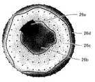
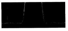
이어서, 상기한 플라즈마 에칭 처리 방법 및 처리 장치에서 발생시킨 마이크로파 플라즈마에 있어서, 유지대(14)와 유전판(16)의 간격 및 플라즈마의 균일성에 대하여 설명한다. 도 7, 도 8, 도 9 및 도 10은 소정 조건하에서의 플라즈마의 분포를 나타낸다. 도 7 및 도 9는 간격이 105 mm인 경우를 나타내고, 도 8 및 도 10은 간격이 85 mm인 경우를 나타낸다. 또한, 도 7 및 도 8과 도 9 및 도 10은 각각 간격의 상이를 제외하고 동일한 조건이다. 또한, 도 7 ~ 도 10 중의 영역(25a, 25b, 25c, 26a, 26b, 26c, 26d)은 각각 플라즈마의 농도가 거의 동일한 영역을 나타낸다. 영역(25a, 25b, 25c)의 순서 및 영역(26a, 26b, 26c, 26d)의 순서로 농도가 진해진다.Next, in the microwave plasma generated by the above-described plasma etching processing method and processing apparatus, the spacing between the
도 7 및 도 8을 참조하면, 간격이 85 mm인 경우에 비해 간격이 105 mm인 경우가 플라즈마의 농도 분포의 격차가 작다. 또한, 도 9 및 도 10을 참조하면, 이 경우도 간격이 85 mm인 경우에 비해 간격이 105 mm인 경우가 플라즈마의 농도 분포의 격차가 작다. 즉, 간격을 100 mm 이상으로 함으로써, 플라즈마의 농도 분포를 균일하게 할 수 있다.Referring to FIGS. 7 and 8, the difference in plasma concentration distribution is smaller in the case where the interval is 105 mm than in the case where the interval is 85 mm. 9 and 10, the gap in the concentration distribution of the plasma is smaller in this case as well in the case where the interval is 105 mm compared with the case where the interval is 85 mm. That is, by making the
여기서, 유지대(14)와 유전판(16)의 간격을 100 mm 이상으로 하고, 처리 용 기(12) 내의 압력을 50 mTorr 이상으로 한다. 이렇게 함으로써, 플라즈마 에칭 처리에 필요한 플라즈마를 균일하게 한 상태에서, 높은 전자 온도를 가지는 플라즈마를 줄여서 플라즈마 에칭 처리를 행할 수 있다. 그러면, 에칭 시에 생성되는 반응 생성물의 재해리를 억제할 수 있어 플라즈마 에칭 처리시에 마이크로 로딩 효과 또는 조밀 형상 차를 억제하고, 선택비의 저하를 방지할 수 있다. 또한, 이러한 비교적 고압의 조건에서는, 설비 상의 관점에서 용이하게 플라즈마 에칭 처리를 행할 수 있다. 따라서, 플라즈마 에칭 처리시에 형상 제어를 용이하게 또한 적절하게 행할 수 있다.Here, the space | interval of the holding
이 경우, 미리 유지대(14)와 유전판(16)의 간격을 100 mm 이상으로 하여 장치를 형성해도 좋고, 예를 들면 유지대(14)를 상하 방향으로 이동 가능한 구성으로 하고, 제어부에 의한 제어에 따라 유지대(14)의 상하 방향의 높이를 조정하여 유지대(14)와 유전판(16)의 간격을 100 mm 이상으로 해도 좋다.In this case, the device may be formed with the interval between the holding table 14 and the
바람직하게는, 처리 용기(12) 내의 압력을 200 mTorr 이하로 한다. 이와 같이 구성함으로써, 보다 적절하게 플라즈마 에칭 처리를 행할 수 있다.Preferably, the pressure in the
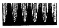
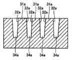
이어서, 상기한 플라즈마 에칭 처리를 행했을 때의 반도체 기판과, 평행 평판형 플라즈마(CCP)(Capacitive Coupled Plasma)에 의해 에칭 처리를 행했을 때의 반도체 기판과의 형상의 차이에 대하여 설명한다. 도 11, 도 12, 도 13 및 도 14는 반도체 기판 상에 형성된 돌출 형상부를 포함하는 층을 에칭했을 때의 반도체 기판의 일부를 나타내는 전자 현미경 사진이다. 도 11은 평행 평판형 CCP에 의해 에칭 처리를 행했을 경우를 나타내고, 도 12는 도 11에 나타낸 돌출 형상부의 확대 사진 이다. 도 13은 상기한 플라즈마 에칭 처리를 행했을 경우를 나타내고, 도 14는 도 13에 나타낸 돌출 형상부의 확대 사진이다. 또한, 도 11에 대응하는 모식도를 도 15에, 도 12에 대응하는 모식도를 도 16에, 도 13에 대응하는 모식도를 도 17에, 도 14에 대응하는 모식도를 도 18에 도시한다.Next, the difference between the shape of the semiconductor substrate at the time of performing the said plasma etching process, and the semiconductor substrate at the time of performing an etching process by parallel planar plasma (CCP) (Capacitive Coupled Plasma) is demonstrated. FIG. 11, FIG. 12, FIG. 13, and FIG. 14 are electron micrographs showing a part of the semiconductor substrate when the layer including the projecting portion formed on the semiconductor substrate is etched. FIG. 11 shows the case where the etching treatment is performed by the parallel plate type CCP, and FIG. 12 is an enlarged photograph of the protruding portion shown in FIG. 11. FIG. 13 shows a case where the above-described plasma etching process is performed, and FIG. 14 is an enlarged photograph of the protruding portion shown in FIG. 13. In addition, the schematic diagram corresponding to FIG. 11 is shown in FIG. 15, the schematic diagram corresponding to FIG. 12 is shown in FIG. 16, the schematic diagram corresponding to FIG. 13 is shown in FIG. 17, and the schematic diagram corresponding to FIG. 14 is shown in FIG.
도 11, 도 12, 도 15 및 도 16을 참조하면, 평행 평판형 플라즈마(CCP)에서 돌출 형상부(31a)의 측벽(32a)에 퇴적되는 디포지션(deposition)은 많고, 저면(33a)과 측벽(32a)의 각도 α는 큰 둔각이다. 또한, 인접하는 돌출 형상부(31a) 간에 형성되는 오목부(34a)가 충분히 움푹 들어간 형상으로 되어 있지 않다. 이에 대하여, 도 13, 도 14, 도 17 및 도 18을 참조하면, 상기한 마이크로파 플라즈마에서, 돌출 형상부(31b)의 측벽(32b)에 퇴적되는 디포지션은 적고, 저면(33b)과 측벽(32b)의 각도 β는 각도 α보다 직각에 가깝게 되어 있다. 또한, 인접하는 돌출 형상부(31b) 간에 형성되는 오목부(34b)도 충분히 움푹 들어간 형상으로 되어 있다. 즉, CCP에 의해 에칭 처리를 행했을 경우에 비해, 상기한 플라즈마 에칭 처리를 행했을 경우, 마이크로 로딩 효과 및 조밀 형상 차가 억제되었다.11, 12, 15, and 16, in the parallel plate type plasma (CCP), deposition is deposited on the
또한, 이러한 플라즈마 에칭 처리는 3 차원 구조를 가지는 반도체 기판에서도 적용된다. 도 19는 종래의 3 차원 구조를 가지는 반도체 기판의 일부를 나타내는 전자 현미경 사진이다. 도 20은, 상기한 플라즈마 에칭 처리를 행한 반도체 기판의 일부를 나타내는 전자 현미경 사진이다. 도 19 및 도 20을 참조하면, 종래에는 반도체 기판(36a) 상의 게이트 산화막(37a)은 크게 에칭되고 있는 데 반해, 상기한 플라즈마 에칭 처리에서는 반도체 기판(36b) 상의 게이트 산화막(37b)은 도 19에 나타낸 게이트 산화막(37a)만큼 에칭되지 않았다. 이와 같이 하여, 선택비의 저하를 방지할 수 있다.This plasma etching process is also applied to a semiconductor substrate having a three-dimensional structure. 19 is an electron micrograph showing a portion of a semiconductor substrate having a conventional three-dimensional structure. 20 is an electron micrograph showing a part of the semiconductor substrate subjected to the plasma etching process described above. 19 and 20, while the
여기서, 거리(L)를 변경한 경우에 있어서의 반도체 기판의 에칭 처리 후 상태의 일부를 도 21 및 도 22의 전자 현미경 사진으로 나타낸다. 도 21은 거리(L)를 135 mm로 한 경우, 도 22는 거리(L)를 275 mm로 한 경우이다. 도 21 및 도 22를 참조하면, 거리(L)를 135 mm로 하여 에칭 처리를 행한 경우보다, 거리(L)를 275 mm로 하여 에칭 처리를 행한 경우 돌출 형상부 선단(先端)의 형상이 가진런해져 균일해진다.Here, a part of the state after the etching process of the semiconductor substrate in the case where distance L is changed is shown by the electron micrograph of FIG. 21 and FIG. FIG. 21 shows the case where the distance L is 135 mm, and FIG. 22 shows the case where the distance L is 275 mm. Referring to FIGS. 21 and 22, the shape of the tip of the protruding portion has a larger shape when the etching process is performed at a distance L of 275 mm than the etching process at a distance L of 135 mm. It becomes uniform.
또한, 이러한 플라즈마 에칭 처리, 구체적으로는 마이크로파 플라즈마에 의해 유지대와 유전판의 간격을 100 mm 이상으로 하고, 처리 용기 내의 압력을 50 mTorr 이상으로 한 플라즈마 에칭 처리는, 반도체 기판에의 플라즈마 데미지가 적다. 따라서, 후술하는 플라즈마 데미지가 적은 실리콘층을 형성하는 경우에 있어서 상당히 효과적이다.In addition, such plasma etching treatment, specifically, the plasma etching treatment in which the distance between the holding table and the dielectric plate is 100 mm or more and the pressure in the processing container is 50 mTorr or more by microwave plasma, causes plasma damage to the semiconductor substrate. little. Therefore, it is quite effective when forming the silicon layer with less plasma damage mentioned later.
도 23은 종래에 있어서 ICP 등의 플라즈마 처리에 의해 플라즈마 데미지를 받은 실리콘층 상에 희생 산화막을 형성하고 이를 에칭하여, 플라즈마 데미지가 적은 실리콘층을 형성하는 공정을 도시하는 개략도이다. 도 23 중 (A)는 플라즈마 에칭 처리에 의해 플라즈마 데미지층이 형성되는 공정, (B)는 플라즈마 데미지층에 희생 산화막을 형성하는 공정, (C)는 형성한 희생 산화막을 웨트 에칭에 의해 제거하는 공정을 도시한다.FIG. 23 is a schematic diagram showing a process of forming a sacrificial oxide film on a silicon layer subjected to plasma damage by plasma treatment such as ICP in the related art and etching the same to form a silicon layer having less plasma damage. In FIG. 23, (A) is a step of forming a plasma damage layer by a plasma etching process, (B) is a step of forming a sacrificial oxide film on the plasma damage layer, (C) is a step of removing the formed sacrificial oxide film by wet etching. The process is shown.
도 23을 참조하면, 종래에는 실리콘층(41)에 대하여 ICP 등에 의한 플라즈마 에칭 처리를 행한 후에 플라즈마 데미지층(42)이 형성된다(A). 플라즈마 데미지층(42)을 제거하기 위하여 플라즈마 데미지층(42)에 대해서 열산화를 행하여 희생 산화막(43)을 형성한다. 그리고, 형성된 희생 산화막(43)을 불소산(HF) 등을 이용하여 데미지가 적은 웨트 에칭에 의해 제거한다. 이와 같이 하여, 플라즈마 데미지가 적은 표면(44)을 가지는 실리콘층(41)을 형성하고 있다. 이러한 공정에서는, 열산화 처리를 포함하기 때문에, 고온에서의 처리를 피하고자 하는 경우에 적용하는 것은 어렵다. 또한, 웨트 에칭 공정을 포함하기 때문에, 처리 장치의 구성이 복잡화된다.Referring to Fig. 23, conventionally,
여기서, 상기한 이 발명에 따른 플라즈마 에칭 처리 방법 및 처리 장치를 이용함으로써, 플라즈마 데미지가 적은 실리콘층을 형성하는 공정을 간소화할 수 있다.Here, by using the above-described plasma etching processing method and processing apparatus according to the present invention, the step of forming a silicon layer with less plasma damage can be simplified.
플라즈마 데미지가 적은 실리콘층을 형성하는 제 1 실시예로서, 종래의 ICP 등의 플라즈마를 이용한 에칭 처리를 행하고, 이 후에 상기한 플라즈마 에칭 처리를 행한다. 이렇게 함으로써, 상기한 플라즈마 에칭 처리를 행한 후에는, 플라즈마에 의한 데미지가 적은 실리콘층을 형성할 수 있다. 이 경우, 예를 들면 CF4와 O2의 반응 가스를 이용하여 반도체 기판에 바이어스를 인가하지 않고, 자기(自己) 바이어스에 의해 플라즈마 처리를 행함으로써, 더욱 데미지를 줄일 수 있다. 이러한 구성에 따르면, 상기한 도 23의 (B) 공정 및 (C) 공정을 생략할 수 있다.As a first embodiment of forming a silicon layer with less plasma damage, an etching process using plasma such as a conventional ICP is performed, followed by the above-described plasma etching process. By doing in this way, after performing said plasma etching process, the silicon layer with little damage by a plasma can be formed. In this case, the damage can be further reduced by performing plasma processing by self bias without applying a bias to the semiconductor substrate using, for example, a reaction gas of CF4 and O2 . According to such a structure, process (B) and process (C) of FIG. 23 mentioned above can be skipped.
플라즈마 데미지가 적은 실리콘층을 형성하는 제 2 실시예로서, 상기한 플라 즈마 에칭 처리를 행한 후, 종래의 열산화 및 웨트 에칭을 행하여, 플라즈마에 의한 데미지가 적은 실리콘층을 형성한다. 이 경우, 플라즈마 에칭 처리에 의한 실리콘층의 데미지가 적기 때문에, 도 23의 (B) 공정 및 (C) 공정의 단축화를 도모할 수 있다.As a second embodiment of forming a silicon layer with less plasma damage, after the plasma etching process described above, conventional thermal oxidation and wet etching are performed to form a silicon layer with little damage by plasma. In this case, since the damage of the silicon layer by plasma etching process is small, the process of FIG. 23 (B) and (C) can be shortened.
플라즈마 데미지가 적은 실리콘층을 형성하는 제 3 실시예로서 일반적인 마이크로파 플라즈마 처리를 행한 후, 상기한 플라즈마 에칭 처리를 행한다. 이렇게 함으로써도, 플라즈마에 의한 데미지가 적은 실리콘층을 형성할 수 있다. 이 경우도 상기한 도 23의 (B) 공정 및 (C) 공정을 생략할 수 있다.As a third embodiment in which a silicon layer having a low plasma damage is formed, a general microwave plasma process is performed, followed by the plasma etching process. By doing this, the silicon layer with little damage by plasma can be formed. Also in this case, process (B) and process (C) of FIG. 23 can be omitted.
또한, 상기의 실시예에서는 플라즈마 에칭 처리에 이용되는 반응 가스로서 할로겐계 가스를 포함하는 반응 가스를 이용하는 것으로 했지만, 이에 한정되지 않고, 할로겐계 가스를 포함하지 않는 가스를 반응 가스로 하는 경우에 대해서도 적용된다.Incidentally, in the above embodiment, a reaction gas containing a halogen gas is used as the reaction gas used in the plasma etching process. However, the present invention is not limited thereto, and the gas containing no halogen gas is used as the reaction gas. Apply.
또한, 상기의 실시예에서는, 실리콘층에 대하여 플라즈마 에칭 처리를 행하는 경우에 대하여 설명했지만, 이에 한정되지 않고, 그 밖의 층에 대하여 플라즈마 에칭 처리를 행하는 경우에 대해서도 적용된다.In the above embodiment, the case where the plasma etching process is performed on the silicon layer has been described. However, the present invention is not limited thereto, and the present invention is also applicable to the case where the plasma etching process is performed on other layers.
이상, 도면을 참조하여 이 발명의 실시예를 설명했지만, 이 발명은 도시한 실시예의 것에 한정되지 않는다. 도시한 실시예에 대하여, 이 발명과 동일한 범위 내에서 혹은 균등한 범위 내에서 다양한 수정 또는 변형을 가할 수 있다.As mentioned above, although the Example of this invention was described with reference to drawings, this invention is not limited to what was shown in the Example. For the illustrated embodiment, various modifications or variations can be made within the same range or equivalent range as the present invention.
도 1은 이 발명의 일 실시예에 따른 플라즈마 처리 장치의 주요부를 도시하는 개략 단면도이다.1 is a schematic cross-sectional view showing a main part of a plasma processing apparatus according to an embodiment of the present invention.
도 2는 마이크로파 플라즈마 및 ICP의 전자 에너지와 전자 에너지 분포 함수와의 관계를 나타내는 그래프이다.2 is a graph showing the relationship between electron energy and electron energy distribution function of microwave plasma and ICP.
도 3은 유전판으로부터의 거리와 플라즈마의 전자 밀도와의 관계를 나타내는 그래프이며, 거리가 100 mm 미만인 경우를 나타낸다.3 is a graph showing the relationship between the distance from the dielectric plate and the electron density of the plasma, and shows a case where the distance is less than 100 mm.
도 4는 유전판으로부터의 거리와 플라즈마의 전자 밀도와의 관계를 나타내는 그래프이며, 거리가 100 mm 이상인 경우를 나타낸다.4 is a graph showing the relationship between the distance from the dielectric plate and the electron density of the plasma, and shows a case where the distance is 100 mm or more.
도 5는 처리 용기 내의 압력과 플라즈마의 전자 밀도와의 관계를 나타내는 그래프이다.5 is a graph showing the relationship between the pressure in the processing vessel and the electron density of plasma.
도 6은 처리 용기 내의 압력과 플라즈마의 최대 전자 온도와의 관계를 나타내는 그래프이다.6 is a graph showing the relationship between the pressure in the processing vessel and the maximum electron temperature of the plasma.
도 7은 소정 조건하에서 간격을 105 mm로 한 경우의 플라즈마의 분포를 나타내는 도이다.Fig. 7 is a diagram showing the distribution of plasma when the interval is 105 mm under predetermined conditions.
도 8은 소정 조건하에서 간격을 85 mm로 한 경우의 플라즈마의 분포를 나타내는 도이다.Fig. 8 is a diagram showing the distribution of plasma when the interval is 85 mm under predetermined conditions.
도 9는 소정 조건하에서 간격을 105 mm로 한 경우의 플라즈마의 분포를 나타내는 도이다.Fig. 9 is a diagram showing the distribution of plasma when the interval is 105 mm under predetermined conditions.
도 10은 소정 조건하에서 간격을 85 mm로 한 경우의 플라즈마의 분포를 나타 내는 도이다.Fig. 10 is a diagram showing the distribution of plasma when the interval is 85 mm under predetermined conditions.
도 11은 CCP에 의해 에칭 처리를 행한 경우의 반도체 기판의 일부를 나타내는 전자 현미경 사진이다.11 is an electron micrograph showing a part of a semiconductor substrate in the case of performing an etching process by CCP.
도 12는 도 11에 나타낸 돌출 형상부의 확대 사진이다.12 is an enlarged photograph of the protruding portion shown in FIG. 11.
도 13은 이 발명의 일 실시예에 따른 플라즈마 에칭 처리를 행한 경우의 반도체 기판의 일부를 나타내는 전자 현미경 사진이다.FIG. 13 is an electron micrograph showing a part of a semiconductor substrate when a plasma etching process is performed according to an embodiment of the present invention. FIG.
도 14는 도 13에 나타낸 돌출 형상부의 확대 사진이다.14 is an enlarged photograph of the protruding portion shown in FIG. 13.
도 15는 도 11에 나타낸 부분의 모식도이다.It is a schematic diagram of the part shown in FIG.
도 16은 도 12에 나타낸 부분의 모식도이다.It is a schematic diagram of the part shown in FIG.
도 17은 도 13에 나타낸 부분의 모식도이다.It is a schematic diagram of the part shown in FIG.
도 18은 도 14에 나타낸 부분의 모식도이다.It is a schematic diagram of the part shown in FIG.
도 19는 종래의 3 차원 구조를 가지는 반도체 기판의 일부를 나타내는 전자 현미경 사진이다.19 is an electron micrograph showing a portion of a semiconductor substrate having a conventional three-dimensional structure.
도 20은 이 발명의 일 실시예에 따른 플라즈마 에칭 처리 방법을 행한 3 차원 구조를 가지는 반도체 기판의 일부를 나타내는 전자 현미경 사진이다.20 is an electron micrograph showing a portion of a semiconductor substrate having a three-dimensional structure in which a plasma etching treatment method is performed in accordance with an embodiment of the present invention.
도 21은 거리를 135 mm로 하여 에칭 처리를 행한 반도체 기판의 일부의 전자 현미경 사진이다.FIG. 21 is an electron micrograph of a portion of a semiconductor substrate subjected to etching with a distance of 135 mm. FIG.
도 22는 거리를 275 mm로 하여 에칭 처리를 행한 반도체 기판의 일부의 전자 현미경 사진이다.FIG. 22 is an electron micrograph of a portion of a semiconductor substrate subjected to etching with a distance of 275 mm. FIG.
도 23은 종래에 있어서 ICP 등의 플라즈마 처리에 의해 플라즈마 데미지를 받은 실리콘층 상에 희생 산화막을 형성하고 이를 에칭하여, 플라즈마 데미지가 적은 실리콘층을 형성하는 공정을 도시하는 개략도이다.FIG. 23 is a schematic diagram showing a process of forming a sacrificial oxide film on a silicon layer subjected to plasma damage by plasma treatment such as ICP in the related art and etching the same to form a silicon layer having less plasma damage.
*** 도면의 주요 부분에 대한 부호의 설명 ***DESCRIPTION OF THE REFERENCE SYMBOLS
11 : 플라즈마 에칭 처리 장치11: plasma etching processing apparatus
12 : 처리 용기12: processing container
13 : 가스 샤워 헤드13: gas shower head
14 : 유지대14: holder
15 : 마이크로파 발생기15: microwave generator
16 : 유전판16: dielectric plate
17 : 개구 홀17: opening hole
18 : 지지부18: support part
19 : 오목부19: recess
20a : 상면20a: Top
20b : 하면20b: if
21 : 도파관21: waveguide
22 : 지파판22: tribe
23 : 슬롯 홀23: slot hole
24 : 슬롯 안테나24: slot antenna
25a, 25b, 25c, 26a, 26b, 26c, 26d : 영역Area: 25a, 25b, 25c, 26a, 26b, 26c, 26d
31a, 31b : 돌출 형상부31a, 31b: protruding shape
32a, 32b : 측벽32a, 32b: sidewalls
33a, 33b : 저면33a, 33b: bottom
34a, 34b : 오목부34a, 34b: concave
36a, 36b : 반도체 기판36a, 36b: semiconductor substrate
37a, 37b : 게이트 산화막37a, 37b: gate oxide film
41 : 실리콘층41: silicon layer
42 : 플라즈마 데미지층42: plasma damage layer
43 : 희생 산화막43: sacrificial oxide film
44 : 표면44: surface
Claims (5)
Translated fromKoreanApplications Claiming Priority (2)
| Application Number | Priority Date | Filing Date | Title |
|---|---|---|---|
| JP2008152816AJP2009302181A (en) | 2008-06-11 | 2008-06-11 | Plasma etching method, and plasma etching apparatus |
| JPJP-P-2008-152816 | 2008-06-11 |
Publications (2)
| Publication Number | Publication Date |
|---|---|
| KR20090129332A KR20090129332A (en) | 2009-12-16 |
| KR101147964B1true KR101147964B1 (en) | 2012-05-24 |
Family
ID=41415186
Family Applications (1)
| Application Number | Title | Priority Date | Filing Date |
|---|---|---|---|
| KR1020090048949AExpired - Fee RelatedKR101147964B1 (en) | 2008-06-11 | 2009-06-03 | Plasma etching method and plasma etching apparatus |
Country Status (5)
| Country | Link |
|---|---|
| US (1) | US20090311870A1 (en) |
| JP (1) | JP2009302181A (en) |
| KR (1) | KR101147964B1 (en) |
| CN (2) | CN101604630B (en) |
| TW (1) | TWI405260B (en) |
Families Citing this family (8)
| Publication number | Priority date | Publication date | Assignee | Title |
|---|---|---|---|---|
| JP2009302181A (en)* | 2008-06-11 | 2009-12-24 | Tokyo Electron Ltd | Plasma etching method, and plasma etching apparatus |
| WO2011108663A1 (en)* | 2010-03-04 | 2011-09-09 | 東京エレクトロン株式会社 | Plasma etching method, method for producing semiconductor device, and plasma etching device |
| US8808562B2 (en) | 2011-09-12 | 2014-08-19 | Tokyo Electron Limited | Dry metal etching method |
| JP6890459B2 (en)* | 2017-04-14 | 2021-06-18 | 東京エレクトロン株式会社 | Plasma processing equipment and control method |
| JP7349861B2 (en)* | 2019-09-24 | 2023-09-25 | 東京エレクトロン株式会社 | Etching methods, damaged layer removal methods, and storage media |
| CN110797245B (en)* | 2019-10-28 | 2022-11-25 | 北京北方华创微电子装备有限公司 | Semiconductor processing equipment |
| CN112967920B (en)* | 2021-02-01 | 2022-07-19 | 湖南红太阳光电科技有限公司 | Microwave plasma etching device and method |
| CN114429903A (en)* | 2022-01-20 | 2022-05-03 | 长鑫存储技术有限公司 | Semiconductor structure and forming method and manufacturing device thereof |
Citations (3)
| Publication number | Priority date | Publication date | Assignee | Title |
|---|---|---|---|---|
| KR20050039500A (en)* | 2003-10-22 | 2005-04-29 | 캐논 가부시끼가이샤 | Processing apparatus and method |
| JP2005286344A (en)* | 2005-04-22 | 2005-10-13 | Hitachi Ltd | Dry etching apparatus and semiconductor device manufacturing method |
| JP2008085165A (en)* | 2006-09-28 | 2008-04-10 | Tokyo Electron Ltd | Etching method and method of manufacturing semiconductor device |
Family Cites Families (6)
| Publication number | Priority date | Publication date | Assignee | Title |
|---|---|---|---|---|
| US6942813B2 (en)* | 2003-03-05 | 2005-09-13 | Applied Materials, Inc. | Method of etching magnetic and ferroelectric materials using a pulsed bias source |
| JP3866694B2 (en)* | 2003-07-30 | 2007-01-10 | 株式会社日立ハイテクノロジーズ | LSI device etching method and apparatus |
| JP4563729B2 (en)* | 2003-09-04 | 2010-10-13 | 東京エレクトロン株式会社 | Plasma processing equipment |
| CN100492591C (en)* | 2003-09-04 | 2009-05-27 | 东京毅力科创株式会社 | Plasma processing apparatus |
| WO2006106665A1 (en)* | 2005-03-31 | 2006-10-12 | Tokyo Electron Limited | Method for nitriding substrate and method for forming insulating film |
| JP2009302181A (en)* | 2008-06-11 | 2009-12-24 | Tokyo Electron Ltd | Plasma etching method, and plasma etching apparatus |
- 2008
- 2008-06-11JPJP2008152816Apatent/JP2009302181A/enactivePending
- 2009
- 2009-05-27CNCN200910142332.2Apatent/CN101604630B/ennot_activeExpired - Fee Related
- 2009-05-27CNCN201410837288.8Apatent/CN104616984B/ennot_activeExpired - Fee Related
- 2009-06-03KRKR1020090048949Apatent/KR101147964B1/ennot_activeExpired - Fee Related
- 2009-06-10TWTW098119303Apatent/TWI405260B/ennot_activeIP Right Cessation
- 2009-06-11USUS12/482,698patent/US20090311870A1/ennot_activeAbandoned
Patent Citations (3)
| Publication number | Priority date | Publication date | Assignee | Title |
|---|---|---|---|---|
| KR20050039500A (en)* | 2003-10-22 | 2005-04-29 | 캐논 가부시끼가이샤 | Processing apparatus and method |
| JP2005286344A (en)* | 2005-04-22 | 2005-10-13 | Hitachi Ltd | Dry etching apparatus and semiconductor device manufacturing method |
| JP2008085165A (en)* | 2006-09-28 | 2008-04-10 | Tokyo Electron Ltd | Etching method and method of manufacturing semiconductor device |
Also Published As
| Publication number | Publication date |
|---|---|
| CN104616984B (en) | 2017-09-12 |
| CN101604630B (en) | 2015-01-28 |
| JP2009302181A (en) | 2009-12-24 |
| CN104616984A (en) | 2015-05-13 |
| KR20090129332A (en) | 2009-12-16 |
| TW201003777A (en) | 2010-01-16 |
| CN101604630A (en) | 2009-12-16 |
| US20090311870A1 (en) | 2009-12-17 |
| TWI405260B (en) | 2013-08-11 |
Similar Documents
| Publication | Publication Date | Title |
|---|---|---|
| KR101147964B1 (en) | Plasma etching method and plasma etching apparatus | |
| KR101880831B1 (en) | Method for deep silicon etching using gas pulsing | |
| TWI444109B (en) | Plasma processing device and plasma processing method | |
| JP5706946B2 (en) | Plasma etching method and plasma etching apparatus | |
| KR101744625B1 (en) | Etching method | |
| US8987140B2 (en) | Methods for etching through-silicon vias with tunable profile angles | |
| KR101276262B1 (en) | Apparatus and method for manufacturing semiconductor devices | |
| KR20150109401A (en) | Method of patterning a silicon nitride dielectric film | |
| KR101276258B1 (en) | Apparatus and method for manufacturing semiconductor devices | |
| US20110021029A1 (en) | Plasma etch method to reduce micro-loading | |
| KR102280572B1 (en) | Plasma processing method | |
| JP2017152531A (en) | Substrate processing method | |
| KR102304163B1 (en) | Etching method | |
| US9111727B2 (en) | Plasma tuning rods in microwave resonator plasma sources | |
| TWI731190B (en) | Manufacturing method of semiconductor device | |
| JP2007080982A (en) | Etching method, etching apparatus and semiconductor device manufacturing method | |
| US11201063B2 (en) | Substrate processing method and substrate processing apparatus | |
| KR20200090099A (en) | Method of etching porous membrane | |
| KR20150032662A (en) | Plasma processing apparatus and plasma processing method | |
| KR102751653B1 (en) | Substrate processing method and substrate processing apparatus | |
| KR102419532B1 (en) | Surface Repair Method for Nitride Etching | |
| US10283370B1 (en) | Silicon addition for silicon nitride etching selectivity | |
| CN107690694B (en) | Partial etch memory by flash addition | |
| CN119744436A (en) | Plasma processing method |
Legal Events
| Date | Code | Title | Description |
|---|---|---|---|
| A201 | Request for examination | ||
| PA0109 | Patent application | St.27 status event code:A-0-1-A10-A12-nap-PA0109 | |
| PA0201 | Request for examination | St.27 status event code:A-1-2-D10-D11-exm-PA0201 | |
| PG1501 | Laying open of application | St.27 status event code:A-1-1-Q10-Q12-nap-PG1501 | |
| D13-X000 | Search requested | St.27 status event code:A-1-2-D10-D13-srh-X000 | |
| D14-X000 | Search report completed | St.27 status event code:A-1-2-D10-D14-srh-X000 | |
| R17-X000 | Change to representative recorded | St.27 status event code:A-3-3-R10-R17-oth-X000 | |
| E902 | Notification of reason for refusal | ||
| PE0902 | Notice of grounds for rejection | St.27 status event code:A-1-2-D10-D21-exm-PE0902 | |
| E13-X000 | Pre-grant limitation requested | St.27 status event code:A-2-3-E10-E13-lim-X000 | |
| P11-X000 | Amendment of application requested | St.27 status event code:A-2-2-P10-P11-nap-X000 | |
| P13-X000 | Application amended | St.27 status event code:A-2-2-P10-P13-nap-X000 | |
| E902 | Notification of reason for refusal | ||
| PE0902 | Notice of grounds for rejection | St.27 status event code:A-1-2-D10-D21-exm-PE0902 | |
| E701 | Decision to grant or registration of patent right | ||
| PE0701 | Decision of registration | St.27 status event code:A-1-2-D10-D22-exm-PE0701 | |
| GRNT | Written decision to grant | ||
| PR0701 | Registration of establishment | St.27 status event code:A-2-4-F10-F11-exm-PR0701 | |
| PR1002 | Payment of registration fee | St.27 status event code:A-2-2-U10-U11-oth-PR1002 Fee payment year number:1 | |
| PG1601 | Publication of registration | St.27 status event code:A-4-4-Q10-Q13-nap-PG1601 | |
| FPAY | Annual fee payment | Payment date:20150416 Year of fee payment:4 | |
| PR1001 | Payment of annual fee | St.27 status event code:A-4-4-U10-U11-oth-PR1001 Fee payment year number:4 | |
| FPAY | Annual fee payment | Payment date:20160418 Year of fee payment:5 | |
| PR1001 | Payment of annual fee | St.27 status event code:A-4-4-U10-U11-oth-PR1001 Fee payment year number:5 | |
| FPAY | Annual fee payment | Payment date:20170421 Year of fee payment:6 | |
| PR1001 | Payment of annual fee | St.27 status event code:A-4-4-U10-U11-oth-PR1001 Fee payment year number:6 | |
| FPAY | Annual fee payment | Payment date:20180502 Year of fee payment:7 | |
| PR1001 | Payment of annual fee | St.27 status event code:A-4-4-U10-U11-oth-PR1001 Fee payment year number:7 | |
| FPAY | Annual fee payment | Payment date:20190429 Year of fee payment:8 | |
| PR1001 | Payment of annual fee | St.27 status event code:A-4-4-U10-U11-oth-PR1001 Fee payment year number:8 | |
| PR1001 | Payment of annual fee | St.27 status event code:A-4-4-U10-U11-oth-PR1001 Fee payment year number:9 | |
| PR1001 | Payment of annual fee | St.27 status event code:A-4-4-U10-U11-oth-PR1001 Fee payment year number:10 | |
| PR1001 | Payment of annual fee | St.27 status event code:A-4-4-U10-U11-oth-PR1001 Fee payment year number:11 | |
| PR1001 | Payment of annual fee | St.27 status event code:A-4-4-U10-U11-oth-PR1001 Fee payment year number:12 | |
| PC1903 | Unpaid annual fee | St.27 status event code:A-4-4-U10-U13-oth-PC1903 Not in force date:20240516 Payment event data comment text:Termination Category : DEFAULT_OF_REGISTRATION_FEE | |
| PC1903 | Unpaid annual fee | St.27 status event code:N-4-6-H10-H13-oth-PC1903 Ip right cessation event data comment text:Termination Category : DEFAULT_OF_REGISTRATION_FEE Not in force date:20240516 |