KR101147427B1 - Organic light emitting display and driving method thereof - Google Patents
Organic light emitting display and driving method thereofDownload PDFInfo
- Publication number
- KR101147427B1 KR101147427B1KR1020100018685AKR20100018685AKR101147427B1KR 101147427 B1KR101147427 B1KR 101147427B1KR 1020100018685 AKR1020100018685 AKR 1020100018685AKR 20100018685 AKR20100018685 AKR 20100018685AKR 101147427 B1KR101147427 B1KR 101147427B1
- Authority
- KR
- South Korea
- Prior art keywords
- voltage
- light emitting
- current
- organic light
- driving
- Prior art date
- Legal status (The legal status is an assumption and is not a legal conclusion. Google has not performed a legal analysis and makes no representation as to the accuracy of the status listed.)
- Active
Links
- 238000000034methodMethods0.000titleclaimsabstractdescription39
- 230000008859changeEffects0.000claimsabstractdescription19
- 230000006866deteriorationEffects0.000claimsdescription18
- 238000012546transferMethods0.000claimsdescription5
- 230000006698inductionEffects0.000claims1
- 238000012937correctionMethods0.000abstractdescription2
- 238000010586diagramMethods0.000description22
- 239000003990capacitorSubstances0.000description20
- 230000015556catabolic processEffects0.000description15
- 238000006731degradation reactionMethods0.000description15
- 230000004044responseEffects0.000description15
- 239000011159matrix materialSubstances0.000description6
- 238000001514detection methodMethods0.000description5
- 101100478997Saccharomyces cerevisiae (strain ATCC 204508 / S288c) SWC3 geneProteins0.000description4
- 230000008569processEffects0.000description4
- 229920001621AMOLEDPolymers0.000description2
- 238000007796conventional methodMethods0.000description2
- 239000000463materialSubstances0.000description2
- 102100035925DNA methyltransferase 1-associated protein 1Human genes0.000description1
- 101000930289Homo sapiens DNA methyltransferase 1-associated protein 1Proteins0.000description1
- 101000667209Homo sapiens Vacuolar protein sorting-associated protein 72 homologProteins0.000description1
- 101150102320SWC3 geneProteins0.000description1
- 102100039098Vacuolar protein sorting-associated protein 72 homologHuman genes0.000description1
- 230000008901benefitEffects0.000description1
- 230000005540biological transmissionEffects0.000description1
- 230000000593degrading effectEffects0.000description1
- 239000004973liquid crystal related substanceSubstances0.000description1
- 238000012986modificationMethods0.000description1
- 230000004048modificationEffects0.000description1
- 230000006798recombinationEffects0.000description1
- 238000005215recombinationMethods0.000description1
- 239000010409thin filmSubstances0.000description1
- 238000004804windingMethods0.000description1
Images


Classifications
- G—PHYSICS
- G09—EDUCATION; CRYPTOGRAPHY; DISPLAY; ADVERTISING; SEALS
- G09G—ARRANGEMENTS OR CIRCUITS FOR CONTROL OF INDICATING DEVICES USING STATIC MEANS TO PRESENT VARIABLE INFORMATION
- G09G3/00—Control arrangements or circuits, of interest only in connection with visual indicators other than cathode-ray tubes
- G09G3/20—Control arrangements or circuits, of interest only in connection with visual indicators other than cathode-ray tubes for presentation of an assembly of a number of characters, e.g. a page, by composing the assembly by combination of individual elements arranged in a matrix no fixed position being assigned to or needed to be assigned to the individual characters or partial characters
- G09G3/22—Control arrangements or circuits, of interest only in connection with visual indicators other than cathode-ray tubes for presentation of an assembly of a number of characters, e.g. a page, by composing the assembly by combination of individual elements arranged in a matrix no fixed position being assigned to or needed to be assigned to the individual characters or partial characters using controlled light sources
- G09G3/30—Control arrangements or circuits, of interest only in connection with visual indicators other than cathode-ray tubes for presentation of an assembly of a number of characters, e.g. a page, by composing the assembly by combination of individual elements arranged in a matrix no fixed position being assigned to or needed to be assigned to the individual characters or partial characters using controlled light sources using electroluminescent panels
- G09G3/32—Control arrangements or circuits, of interest only in connection with visual indicators other than cathode-ray tubes for presentation of an assembly of a number of characters, e.g. a page, by composing the assembly by combination of individual elements arranged in a matrix no fixed position being assigned to or needed to be assigned to the individual characters or partial characters using controlled light sources using electroluminescent panels semiconductive, e.g. using light-emitting diodes [LED]
- G09G3/3208—Control arrangements or circuits, of interest only in connection with visual indicators other than cathode-ray tubes for presentation of an assembly of a number of characters, e.g. a page, by composing the assembly by combination of individual elements arranged in a matrix no fixed position being assigned to or needed to be assigned to the individual characters or partial characters using controlled light sources using electroluminescent panels semiconductive, e.g. using light-emitting diodes [LED] organic, e.g. using organic light-emitting diodes [OLED]
- G09G3/3225—Control arrangements or circuits, of interest only in connection with visual indicators other than cathode-ray tubes for presentation of an assembly of a number of characters, e.g. a page, by composing the assembly by combination of individual elements arranged in a matrix no fixed position being assigned to or needed to be assigned to the individual characters or partial characters using controlled light sources using electroluminescent panels semiconductive, e.g. using light-emitting diodes [LED] organic, e.g. using organic light-emitting diodes [OLED] using an active matrix
- G09G3/3233—Control arrangements or circuits, of interest only in connection with visual indicators other than cathode-ray tubes for presentation of an assembly of a number of characters, e.g. a page, by composing the assembly by combination of individual elements arranged in a matrix no fixed position being assigned to or needed to be assigned to the individual characters or partial characters using controlled light sources using electroluminescent panels semiconductive, e.g. using light-emitting diodes [LED] organic, e.g. using organic light-emitting diodes [OLED] using an active matrix with pixel circuitry controlling the current through the light-emitting element
- G—PHYSICS
- G09—EDUCATION; CRYPTOGRAPHY; DISPLAY; ADVERTISING; SEALS
- G09G—ARRANGEMENTS OR CIRCUITS FOR CONTROL OF INDICATING DEVICES USING STATIC MEANS TO PRESENT VARIABLE INFORMATION
- G09G3/00—Control arrangements or circuits, of interest only in connection with visual indicators other than cathode-ray tubes
- G09G3/20—Control arrangements or circuits, of interest only in connection with visual indicators other than cathode-ray tubes for presentation of an assembly of a number of characters, e.g. a page, by composing the assembly by combination of individual elements arranged in a matrix no fixed position being assigned to or needed to be assigned to the individual characters or partial characters
- G09G3/22—Control arrangements or circuits, of interest only in connection with visual indicators other than cathode-ray tubes for presentation of an assembly of a number of characters, e.g. a page, by composing the assembly by combination of individual elements arranged in a matrix no fixed position being assigned to or needed to be assigned to the individual characters or partial characters using controlled light sources
- G09G3/30—Control arrangements or circuits, of interest only in connection with visual indicators other than cathode-ray tubes for presentation of an assembly of a number of characters, e.g. a page, by composing the assembly by combination of individual elements arranged in a matrix no fixed position being assigned to or needed to be assigned to the individual characters or partial characters using controlled light sources using electroluminescent panels
- G09G3/32—Control arrangements or circuits, of interest only in connection with visual indicators other than cathode-ray tubes for presentation of an assembly of a number of characters, e.g. a page, by composing the assembly by combination of individual elements arranged in a matrix no fixed position being assigned to or needed to be assigned to the individual characters or partial characters using controlled light sources using electroluminescent panels semiconductive, e.g. using light-emitting diodes [LED]
- G—PHYSICS
- G09—EDUCATION; CRYPTOGRAPHY; DISPLAY; ADVERTISING; SEALS
- G09G—ARRANGEMENTS OR CIRCUITS FOR CONTROL OF INDICATING DEVICES USING STATIC MEANS TO PRESENT VARIABLE INFORMATION
- G09G5/00—Control arrangements or circuits for visual indicators common to cathode-ray tube indicators and other visual indicators
- G—PHYSICS
- G09—EDUCATION; CRYPTOGRAPHY; DISPLAY; ADVERTISING; SEALS
- G09G—ARRANGEMENTS OR CIRCUITS FOR CONTROL OF INDICATING DEVICES USING STATIC MEANS TO PRESENT VARIABLE INFORMATION
- G09G2320/00—Control of display operating conditions
- G09G2320/02—Improving the quality of display appearance
- G09G2320/029—Improving the quality of display appearance by monitoring one or more pixels in the display panel, e.g. by monitoring a fixed reference pixel
- G09G2320/0295—Improving the quality of display appearance by monitoring one or more pixels in the display panel, e.g. by monitoring a fixed reference pixel by monitoring each display pixel
- G—PHYSICS
- G09—EDUCATION; CRYPTOGRAPHY; DISPLAY; ADVERTISING; SEALS
- G09G—ARRANGEMENTS OR CIRCUITS FOR CONTROL OF INDICATING DEVICES USING STATIC MEANS TO PRESENT VARIABLE INFORMATION
- G09G2320/00—Control of display operating conditions
- G09G2320/04—Maintaining the quality of display appearance
- G09G2320/043—Preventing or counteracting the effects of ageing
- G09G2320/045—Compensation of drifts in the characteristics of light emitting or modulating elements
Landscapes
- Engineering & Computer Science (AREA)
- Physics & Mathematics (AREA)
- Computer Hardware Design (AREA)
- General Physics & Mathematics (AREA)
- Theoretical Computer Science (AREA)
- Electroluminescent Light Sources (AREA)
- Control Of El Displays (AREA)
Abstract
Translated fromKoreanDescription
Translated fromKorean본 발명은 유기 발광 표시 장치 및 그의 구동 방법에 관한 것으로, 더욱 상세하게는 유기 발광 다이오드의 열화를 빠르게 보상하고 구동 트랜지스터의 문턱 전압 및 이동도와 무관하게 균일한 휘도의 영상을 표시할 수 있는 유기 발광 표시 장치와 그의 구동 방법에 관한 것이다.The present invention relates to an organic light emitting diode display and a driving method thereof. More particularly, the present invention relates to an organic light emitting diode capable of quickly compensating degradation of an organic light emitting diode and displaying an image having a uniform luminance regardless of threshold voltage and mobility of a driving transistor. A display device and its driving method.
근래에 와서, 음극선관(Cathode Ray Tube)의 단점인 무게와 부피를 줄일 수 있는 각종 평판 표시 장치들이 개발되고 있다. 평판 장치로는 액정 표시 장치(Liquid Crystal Display: LCD), 전계 방출 표시 장치(Field Emission Display: FED), 플라즈마 표시 패널(Plasma Display Panel: PDP) 및 유기 발광 표시 장치(Organic Light Emitting Display Device) 등이 있다.In recent years, various flat panel displays have been developed to reduce the weight and volume, which are disadvantages of cathode ray tubes. As a flat panel device, a liquid crystal display (LCD), a field emission display (FED), a plasma display panel (PDP), an organic light emitting display device, etc. There is this.
평판 표시 장치 중 유기 발광 표시 장치는 전자와 정공의 재결합에 의하여 빛을 발생하는 유기 발광 다이오드(Organic Light Emitting Diode, OLED)를 이용하여 영상을 표시하는 것으로서, 빠른 응답속도를 가짐과 동시에 낮은 소비전력으로 구동되고 발광효율, 휘도 및 시야각이 뛰어난 장점이 있어 주목받고 있다.Among the flat panel displays, the organic light emitting diode display displays an image using an organic light emitting diode (OLED) that generates light by recombination of electrons and holes. The organic light emitting diode display has a fast response speed and low power consumption. It has been attracting attention because it has the advantage of excellent luminous efficiency, brightness and viewing angle.
통상적으로, 유기 발광 표시 장치는 유기 발광 다이오드를 구동하는 방식에 따라 패시브 매트릭스형 유기 발광 표시 장치(PMOLED)와 액티브 매트릭스형 유기 발광 표시 장치(AMOLED)로 분류된다.In general, the organic light emitting diode display is classified into a passive matrix organic light emitting diode display (PMOLED) and an active matrix organic light emitting diode display (AMOLED) according to a method of driving the organic light emitting diode.
패시브 매트릭스형은 양극과 음극을 서로 직교하도록 형성하고 음극 라인과 양극 라인을 선택하여 구동하는 방식이고, 액티브 매트릭스형은 박막 트랜지스터와 커패시터를 각 픽셀 내에 집적하여 커패시터 용량에 의해 전압을 유지하도록 하는 구동 방식이다. 패시브 매트릭스형은 구조가 간단하고 염가이지만 대형 또는 고정밀도의 패널 실현이 곤란하다. 반면, 액티브 매트릭스형은 대형 및 고정밀도의 패널 실현이 가능하지만 그 제어방법이 기술적으로 어렵고 비교적 고가라는 문제가 있다.The passive matrix type is a method of forming the anode and cathode to be orthogonal to each other and selects and drives the cathode line and the anode line. The active matrix type is a drive that integrates the thin film transistor and the capacitor in each pixel to maintain the voltage by the capacitor capacity. That's the way. The passive matrix type is simple in structure and inexpensive, but it is difficult to realize a large or high precision panel. On the other hand, the active matrix type can realize a large size and high precision panel, but there is a problem that its control method is technically difficult and relatively expensive.
해상도, 콘트라스트, 동작속도의 관점에서 단위 화소마다 선택하여 점등하는 액티브 매트릭스형 유기 발광 표시 장치(AMOLED)가 주류가 되고 있다.Active matrix organic light emitting display devices (AMOLEDs), which are selected and lighted for each unit pixel in terms of resolution, contrast, and operation speed, have become mainstream.
유기 발광 다이오드의 열화에 의하여 발광 효율이 떨어져, 동일한 전류에 대해 발광 휘도가 떨어지는 문제점이 발생한다.Due to the deterioration of the organic light emitting diode, the luminous efficiency is lowered, resulting in a problem that the luminous brightness falls for the same current.
또한, 유기 발광 다이오드에 흐르는 전류를 제어하는 구동 트랜지스터의 문턱 전압 불균일 및 전자 이동도(electron mobility)의 변화에 따른 데이터 신호의 오차에 의하여 동일한 데이터 신호에 따라 유기 발광 다이오드에 흐르는 전류가 달라지는 문제점이 있다.In addition, the current flowing through the organic light emitting diode is changed according to the same data signal due to an error in the data signal caused by a variation in threshold voltage and electron mobility of the driving transistor controlling the current flowing through the organic light emitting diode. have.
유기 발광 다이오드의 열화는 이미지 스틱킹(image-sticking)의 원인이 되고, 구동 트랜지스터의 특성 편차는 무라(mura)의 원인이 된다.Deterioration of the organic light emitting diode causes image sticking, and characteristic variation of the driving transistor causes mura.
특히 이동도의 불균일에 의한 문제에 있어서, 기존의 방식으로 보상을 하는 경우에는 보상에는 한계가 있고 이로 인해 보정된 픽셀 데이터가 정확하게 각 픽셀별 전류를 매칭시키지 못하여 에러 요인으로 작용하게 되어 이 한계에 대한 문제점이 있다.In particular, in the case of the problem caused by the unevenness of mobility, the compensation is limited in the conventional method, which causes the corrected pixel data to act as an error factor because it does not accurately match the current for each pixel. There is a problem.
유기 발광 다이오드(OLED)의 열화에 따른 휘도 저하 문제를 보상하며, 화소에 포함되는 구동 트랜지스터의 문턱전압/이동도와 무관하게 균일한 휘도의 영상을 표시할 수 있도록 하는 유기전계발광 표시장치를 제공하는 것이다. 또한 기존의 방식은 이동도 보상에는 한계가 있고 이로 인해 보정된 픽셀 데이터가 정확하게 각 픽셀별 전류를 매칭시키지 못하여 에러 요인으로 작용하게 되어, 이를 보정하기 위한 방식을 제공하는 것이다.Provided is an organic light emitting display device that compensates for a problem of deterioration of luminance due to deterioration of an organic light emitting diode (OLED) and displays an image of uniform luminance irrespective of threshold voltage / mobility of a driving transistor included in a pixel. will be. In addition, the conventional method has a limitation in mobility compensation, and as a result, the corrected pixel data does not exactly match the current for each pixel, thereby serving as an error factor, thereby providing a method for correcting the error.
본 발명이 이루고자 하는 기술적 과제들은 이상에서 언급한 기술적 과제들로 제한되지 않으며, 언급되지 않은 또 다른 기술적 과제들은 본 발명의 기재로부터 당해 분야에서 통상의 지식을 가진 자에게 명확하게 이해될 수 있을 것이다.The technical objects to be achieved by the present invention are not limited to the above-mentioned technical problems, and other technical subjects which are not mentioned can be clearly understood by those skilled in the art from the description of the present invention .
상기 목적을 달성하기 위한 본 발명의 일 실시 예에 따른 유기 발광표시 장치는 복수의 유기 발광 다이오드 및 상기 복수의 유기 발광 다이오드 각각에 구동 전류를 공급하는 복수의 구동 트랜지스터 각각을 포함하는 복수의 화소 상기 복수의 화소 각각에 연결된 데이터선을 통해, 유기 발광 다이오드에 이르는 구동 전류의 경로로 소정의 전류를 싱크하는 동안 상기 복수의 구동 트랜지스터 각각의 게이트 전극에 인가되는 소정의 전압을 전달받아 상기 복수의 구동 트랜지스터 각각의 문턱 전압, 이동도 및 이동도의 변화를 구하여 입력 영상 데이터 신호에 따른 보상량을 결정하는 보상부 상기 보상량을 전달받아 입력 영상 데이터 신호를 보정하여 보정된 영상 데이터 신호를 전달하는 타이밍 제어부 및 상기 보정된 영상 데이터 신호에 기초하여 데이터 전압을 생성하고, 상기 복수의 화소에 상기 데이터 전압을 공급하는 데이터 구동부를 포함한다.According to at least one example embodiment of the inventive concepts, an organic light emitting diode display includes a plurality of pixels including a plurality of organic light emitting diodes and a plurality of driving transistors respectively supplying driving currents to the plurality of organic light emitting diodes. The plurality of driving devices receive a predetermined voltage applied to the gate electrode of each of the plurality of driving transistors while sinking a predetermined current through a path of driving current to the organic light emitting diode through a data line connected to each of the plurality of pixels. Compensation unit for determining the compensation amount according to the input image data signal by obtaining the change in the threshold voltage, mobility and mobility of each transistor Timing for transmitting the corrected image data signal by receiving the compensation amount and correcting the input image data signal Based on the controller and the corrected image data signal. Generating the emitter voltage, and a data driver for supplying the data voltage to the pixels.
상기 보상부는, 상기 소정의 전류를 싱크하는 적어도 하나 이상의 전류 싱크부, 상기 문턱 전압, 이동도 및 이동도의 편차를 구하고 상기 보상량을 결정하는 제어부, 및 상기 소정의 전압을 전달받아 저장하고, 상기 결정된 보상량을 저장하는 메모리부를 포함하며, 상기 복수의 화소 각각에 연결된 데이터선을 통해 상기 복수의 유기 발광 다이오드 각각에 소정의 제3 전류를 공급하는 동안 상기 복수의 유기 발광 다이오드 각각의 구동 전압을 대응하는 데이터선을 통해 전달받고, 상기 전달받은 구동 전압에 따라 상기 복수의 유기 발광 다이오드 각각의 열화 정도에 따른 보상량을 결정한다.The compensation unit, at least one current sink unit for sinking the predetermined current, a control unit for determining the compensation amount and the deviation of the threshold voltage, mobility and mobility, and receives and stores the predetermined voltage, A memory unit configured to store the determined compensation amount, and a driving voltage of each of the plurality of organic light emitting diodes while supplying a predetermined third current to each of the plurality of organic light emitting diodes through a data line connected to each of the plurality of pixels. Is received through a corresponding data line, and the compensation amount according to the deterioration degree of each of the plurality of organic light emitting diodes is determined according to the received driving voltage.
상기 전류 싱크부는, 소정의 제1 전류를 싱크하는 제1 전류 싱크부 및 상기 제1 전류보다 전류값이 낮은 제2 전류를 싱크하는 제2 전류 싱크부이고, 상기 제1 전류는 유기 발광 다이오드가 최대 휘도로 발광할 때 상기 유기 발광 다이오드에 흐르는 전류값이며, 상기 제1 전류 및 상기 제2 전류를 싱크하는 동안, 복수의 구동 트랜지스터 각각의 게이트 전극에 제1 전압 및 제2 전압이 인가되고, 상기 제1 전압 및 제2 전압으로부터 상기 복수의 구동 트랜지스터 각각의 문턱 전압 및 이동도가 산출되며, 상기 보상량은 상기 복수의 유기 발광 다이오드 각각의 열화로 인해 증가된 구동 전압에 대응하는 전압값이 된다.The current sink unit is a first current sink unit for sinking a predetermined first current and a second current sink unit for sinking a second current having a lower current value than the first current, wherein the first current is an organic light emitting diode. A value of a current flowing through the organic light emitting diode when emitting light at a maximum brightness, and a first voltage and a second voltage are applied to gate electrodes of each of the plurality of driving transistors while the first current and the second current are sinked, Threshold voltage and mobility of each of the plurality of driving transistors are calculated from the first voltage and the second voltage, and the compensation amount is a voltage value corresponding to an increased driving voltage due to deterioration of each of the plurality of organic light emitting diodes. do.
또한 상기 보상부는, 상기 제3 전류를 공급하는 전류 소스부를 더 포함할 수 있다.In addition, the compensation unit may further include a current source unit for supplying the third current.
본 발명의 상기 유기 발광 표시 장치는 상기 보상부와 데이터 구동부 및 상기 복수의 화소 사이에 선택부를 더 포함하고, 상기 선택부는, 상기 복수의 화소 각각에 연결된 데이터선에 접속되는 복수의 데이터 선택 스위치, 상기 복수의 데이터선 각각에서 분기된 복수의 보상선의 접점에 접속되는 복수의 보상부 선택 스위치, 및 상기 복수의 데이터 선택 스위치 및 복수의 보상부 선택 스위치 각각의 스위칭 동작을 제어하는 복수의 선택 신호를 생성하여 전달하는 선택 구동부를 포함하는 장치일 수 있다.The organic light emitting diode display may further include a selector between the compensator, the data driver, and the plurality of pixels, wherein the selector comprises: a plurality of data select switches connected to data lines connected to each of the plurality of pixels; A plurality of compensation part selection switches connected to contacts of a plurality of compensation lines branched from each of the plurality of data lines, and a plurality of selection signals for controlling switching operations of the plurality of data selection switches and the plurality of compensation part selection switches, respectively. It may be a device including a selection driving unit for generating and delivering.
본 발명의 다른 실시예에 의한 유기 발광 표시 장치는 상기 복수의 화소 각각은, 상기 복수의 유기 발광 다이오드 각각의 일 전극과 상기 복수의 화소 각각에 연결된 데이터선 사이에 위치하는 복수의 제1 트랜지스터, 및 상기 복수의 화소 각각에 연결된 데이터선과 상기 복수의 구동 트랜지스터 각각의 게이트 전극 사이에 위치하는 복수의 제2 트랜지스터를 더 포함한다.According to another exemplary embodiment, an organic light emitting display device includes a plurality of first transistors disposed between one electrode of each of the plurality of organic light emitting diodes and a data line connected to each of the plurality of pixels; And a plurality of second transistors positioned between data lines connected to each of the plurality of pixels and gate electrodes of each of the plurality of driving transistors.
상기 복수의 제1 트랜지스터 및 복수의 제2 트랜지스터 각각이 턴 온 되는 동안, 소정의 전류를 싱크하고 상기 복수의 구동 트랜지스터 각각의 게이트 전극에 인가되는 소정의 전압이 보상부에 전달되고, 상기 복수의 제1 트랜지스터 각각이 턴 온 되고, 상기 복수의 제2 트랜지스터 각각이 턴 오프 되는 동안, 소정의 전류를 공급하고 상기 복수의 유기 발광 다이오드 각각의 구동 전압이 보상부에 전달되며, 상기 복수의 제1 트랜지스터 각각이 턴 오프 되고, 상기 복수의 제2 트랜지스터 각각이 턴 온 되는 동안, 보정된 영상 데이터 신호에 기초한 데이터 전압이 복수의 화소 각각에 공급된다.While each of the plurality of first transistors and the plurality of second transistors is turned on, a predetermined voltage is sinked and a predetermined voltage applied to a gate electrode of each of the plurality of driving transistors is transferred to a compensator, and the plurality of While each of the first transistors is turned on and each of the plurality of second transistors is turned off, a predetermined current is supplied and a driving voltage of each of the plurality of organic light emitting diodes is transferred to a compensator, and the plurality of first While each of the transistors is turned off and each of the plurality of second transistors is turned on, a data voltage based on the corrected image data signal is supplied to each of the plurality of pixels.
상기 목적을 달성하기 위한 본 발명의 일 실시 예에 따른 유기 발광 표시 장치의 구동 방법은 복수의 화소 각각에 대응하는 데이터선을 통해 상기 복수의 화소 각각에 포함되는 구동 트랜지스터를 경유하여 유기 발광 다이오드에 이르는 구동 전류의 경로로 소정의 전류를 싱크하는 동안 상기 복수의 구동 트랜지스터 각각의 게이트 전극에 인가되는 소정의 전압을 전달받는 단계 상기 소정의 전압을 이용하여 상기 복수의 구동 트랜지스터 각각의 문턱 전압, 이동도 및 상기 이동도의 편차를 구하여 입력 영상 데이터 신호에 따른 보상량을 결정하는 단계 및 상기 보상량을 기초로 하여 입력 영상 데이터 신호를 보정하고, 보정된 영상 데이터 신호에 따른 데이터 전압을 생성하여 복수의 화소 각각에 전달하는 단계를 포함한다.According to an exemplary embodiment of the present invention, a driving method of an organic light emitting diode display is provided to an organic light emitting diode via a driving transistor included in each of the plurality of pixels through a data line corresponding to each of the plurality of pixels. Receiving a predetermined voltage applied to a gate electrode of each of the plurality of driving transistors while sinking a predetermined current through a path of driving current leading to the threshold voltage of each of the plurality of driving transistors by using the predetermined voltage. Determining a compensation amount according to the input image data signal by calculating the deviation of the degree and the mobility, and correcting the input image data signal based on the compensation amount, and generating a data voltage according to the corrected image data signal. Delivering to each of the pixels.
상기 소정의 전압을 전달받는 단계는, 제1 전류를 싱크하고, 상기 복수의 구동 트랜지스터 각각의 게이트 전극에 인가되는 제1 전압을 전달받는 단계, 및 상기 제1 전류보다 전류값이 낮은 제2 전류를 싱크하고, 상기 복수의 구동 트랜지스터 각각의 게이트 전극에 인가되는 제2 전압을 전달받는 단계를 포함한다.The receiving of the predetermined voltage may include: sinking a first current, receiving a first voltage applied to a gate electrode of each of the plurality of driving transistors, and a second current having a lower current value than the first current. Sinking and receiving a second voltage applied to a gate electrode of each of the plurality of driving transistors.
상기 제1 전류는 유기 발광 다이오드가 최대 휘도로 발광할 때 상기 유기 발광 다이오드에 흐르는 전류값일 수 있으며, 상기 소정의 전압을 전달받는 단계 이전 또는 이후에, 복수의 화소 각각에 대응하는 데이터선을 통해 상기 복수의 화소 각각에 포함되는 복수의 유기 발광 다이오드 각각에 소정의 제3 전류를 공급하고, 상기 복수의 유기 발광 다이오드 각각의 구동 전압을 전달받는 단계, 및 상기 전달받은 구동 전압에 따라 상기 복수의 유기 발광 다이오드 각각의 열화 정도에 따른 보상량을 결정하는 단계를 더 포함할 수 있다.The first current may be a current value flowing through the organic light emitting diode when the organic light emitting diode emits light at the maximum luminance, and before or after receiving the predetermined voltage, through the data line corresponding to each of the plurality of pixels. Supplying a predetermined third current to each of a plurality of organic light emitting diodes included in each of the plurality of pixels, receiving a driving voltage of each of the plurality of organic light emitting diodes, and the plurality of organic light emitting diodes according to the received driving voltages. The method may further include determining a compensation amount according to the degree of degradation of each organic light emitting diode.
상기 복수의 화소 각각에 대응하는 데이터선을 통해 소정의 전압을 전달받는 단계 및 상기 복수의 화소 각각에 보정된 영상 데이터 신호에 따른 데이터 전압을 전달하는 단계는, 상기 복수의 데이터선에 각각 접속되는 복수의 데이터 선택 스위치 및 상기 복수의 데이터선 각각에서 분기된 복수의 보상선의 접점에 접속되는 복수의 보상부 선택 스위치를 포함하는 선택부의 스위칭 동작에 의해 제어되며,Receiving a predetermined voltage through a data line corresponding to each of the plurality of pixels and transferring a data voltage according to a corrected image data signal to each of the plurality of pixels are connected to the plurality of data lines, respectively. Controlled by a switching operation of a selection unit including a plurality of data selection switches and a plurality of compensation unit selection switches connected to contacts of a plurality of compensation lines branched from each of the plurality of data lines,
상기 선택부는 상기 복수의 데이터 선택 스위치 및 복수의 보상부 선택 스위치 각각의 스위칭 동작을 제어하는 복수의 선택 신호를 생성하여 전달하는 선택 구동부를 더 포함할 수 있다.The selector may further include a select driver configured to generate and transmit a plurality of select signals for controlling switching operations of the plurality of data select switches and the plurality of compensator select switches.
상기 소정의 전압을 전달받는 단계가 수행되는 기간 동안, 상기 복수의 화소 각각의 구동 트랜지스터, 상기 복수의 유기 발광 다이오드 각각의 일 전극 및 상기 대응하는 데이터선 사이에 연결된 복수의 화소 각각의 제1 트랜지스터, 및 상기 대응하는 데이터선 및 상기 구동 트랜지스터의 게이트 전극 사이에 연결된 복수의 화소 각각의 제2 트랜지스터가 턴 온 될 수 있으며, 상기 보정된 영상 데이터 신호에 따른 데이터 전압을 생성하여 복수의 화소 각각에 전달하는 단계가 수행되는 동안, 상기 복수의 유기 발광 다이오드 각각의 일 전극 및 상기 대응하는 데이터선 사이에 연결된 복수의 화소 각각의 제1 트랜지스터가 턴 오프 되고, 상기 복수의 화소 각각의 구동 트랜지스터 및 상기 대응하는 데이터선 및 상기 구동 트랜지스터의 게이트 전극 사이에 연결된 복수의 화소 각각의 제2 트랜지스터가 턴 온 되는 유기 발광 표시 장치의 구동 방법일 수 있다.During the period of receiving the predetermined voltage, the first transistor of each of the plurality of pixels connected between the driving transistor of each of the plurality of pixels, one electrode of each of the plurality of organic light emitting diodes, and the corresponding data line. And a second transistor of each of the plurality of pixels connected between the corresponding data line and the gate electrode of the driving transistor may be turned on, and generates a data voltage according to the corrected image data signal to each of the plurality of pixels. During the transferring, a first transistor of each of the plurality of pixels connected between one electrode of each of the plurality of organic light emitting diodes and the corresponding data line is turned off, and a driving transistor and each of the plurality of pixels is turned off. Between a corresponding data line and a gate electrode of the driving transistor The method may be a method of driving an organic light emitting diode display in which a second transistor of each of a plurality of connected pixels is turned on.
본 발명에 의하면 유기 발광 표시 장치에서 화소들 각각의 트랜지스터의 문턱 전압 불균일과 전자 이동도의 편차로 인한 휘도의 불균일 및 편차를 방지하여 화질을 향상시킬 수 있다.According to the present invention, the image quality can be improved by preventing the variation in luminance and the variation in luminance due to the variation in threshold voltage and electron mobility of each transistor in the OLED display.
또한 본 발명에 의하면 유기 발광 표시 장치의 화소들 각각에 포함되는 유기 발광 다이오드(OLED)의 열화를 실시간으로 빠른 시간 내에 감지하여 이를 보상함으로써 유기 발광 다이오드(OLED)의 열화에 무관하게 목적하는 휘도로 화면을 표시할 수 있다. 아울러 유기 발광 다이오드(OLED)의 열화 감지를 빠르게 실시하면서 동시에 블랙 휘도 달성을 구현하기 힘든 문제점을 극복하여 원하는 레벨의 블랙 휘도를 얻을 수 있다.In addition, according to the present invention, by detecting the degradation of the organic light emitting diode (OLED) included in each of the pixels of the organic light emitting display in real time in a short time to compensate for this to achieve a desired luminance regardless of the degradation of the organic light emitting diode (OLED) The screen can be displayed. In addition, the degradation of the organic light emitting diode (OLED) can be quickly detected, and at the same time, it is possible to obtain a black luminance having a desired level by overcoming the difficulty of achieving black luminance.
본 발명의 경우 새로운 관계식에 의해 보상 데이터를 결정하므로, 즉 구동 트랜지스터의 이동도에 따라 조절된 감마에 따라 데이터 전압을 을 생성하므로, TFT의 이동도 오차 보상 범위가 넓어져 양품 패널을 다수 확보할 수 있고, 각각의 이동도 변화에 대한 테이블 또는 논리 연산식만 보유하고 있으면 되므로 간단하게 양품의 패널을 다수 확보할 수 있는 것이 가능하다.In the present invention, since the compensation data is determined by the new relational expression, that is, the data voltage is generated according to the gamma adjusted according to the mobility of the driving transistor, the mobility compensation range of the TFT is widened to secure a large number of good panels. It is possible to secure a large number of panels of good quality simply because it only needs to have a table or a logical expression for each mobility change.
도 1은 본 발명의 일 실시 예에 의한 유기 발광 표시 장치의 블록도이다.
도 2는 도 1에 도시된 일부 구성과 화소의 일 실시 예에 의한 회로도를 나타낸 도면이다.
도 3 내지 도 6은 화소 및 선택부로 공급되는 일 실시 예에 의한 구동 파형을 나타내는 도면이다.
도 7은 도 1에 도시된 화소의 다른 일 실시 예에 의한 회로도를 나타낸 도면이다.
도 8은 도 7의 화소로 공급되는 일 실시 예에 의한 구동 파형을 나타낸 도면이다.
도 9는 본 발명의 일 실시 예에 의한 유기 발광 표시 장치의 계조별 전류 곡선을 나타내는 그래프이다.1 is a block diagram of an organic light emitting diode display according to an exemplary embodiment.
FIG. 2 is a circuit diagram illustrating a partial configuration and a pixel according to an exemplary embodiment of FIG. 1.
3 to 6 are diagrams illustrating driving waveforms according to an exemplary embodiment supplied to a pixel and a selection unit.
FIG. 7 is a circuit diagram illustrating another pixel of FIG. 1. FIG.
8 is a diagram illustrating a driving waveform according to an embodiment supplied to the pixel of FIG. 7.
9 is a graph illustrating a current curve for each gray level of an organic light emitting diode display according to an exemplary embodiment.
이하, 첨부한 도면을 참고로 하여 본 발명의 실시 예들에 대하여 본 발명이 속하는 기술 분야에서 통상의 지식을 가진 자가 용이하게 실시할 수 있도록 상세히 설명한다. 본 발명은 여러 가지 상이한 형태로 구현될 수 있으며 여기에서 설명하는 실시 예들에 한정되지 않는다.Hereinafter, exemplary embodiments of the present invention will be described in detail with reference to the accompanying drawings, which will be readily apparent to those skilled in the art to which the present invention pertains. The present invention may be embodied in many different forms and is not limited to the embodiments described herein.
또한, 여러 실시 예들에 있어서, 동일한 구성을 가지는 구성요소에 대해서는 동일한 부호를 사용하여 대표적으로 제1 실시 예에서 설명하고, 그 외의 실시 예에서는 제1 실시 예와 다른 구성에 대해서만 설명하기로 한다.In addition, in the various embodiments, components having the same configuration will be representatively described in the first embodiment using the same reference numerals, and in other embodiments, only the configuration different from the first embodiment will be described.
본 발명을 명확하게 설명하기 위해서 설명과 관계없는 부분은 생략하였으며, 명세서 전체를 통하여 동일 또는 유사한 구성요소에 대해서는 동일한 참조 부호를 붙이도록 한다.In order to clearly illustrate the present invention, parts not related to the description are omitted, and the same or similar components are denoted by the same reference numerals throughout the specification.
명세서 전체에서, 어떤 부분이 다른 부분과 "연결"되어 있다고 할 때, 이는 "직접적으로 연결"되어 있는 경우뿐 아니라, 그 중간에 다른 소자를 사이에 두고 "전기적으로 연결"되어 있는 경우도 포함한다. 또한 어떤 부분이 어떤 구성요소를 "포함"한다고 할 때, 이는 특별히 반대되는 기재가 없는 한 다른 구성요소를 제외하는 것이 아니라 다른 구성요소를 더 포함할 수 있는 것을 의미한다.Throughout the specification, when a part is referred to as being "connected" to another part, it includes not only "directly connected" but also "electrically connected" with another part in between . In addition, when a part is said to "include" a certain component, which means that it may further include other components, except to exclude other components unless otherwise stated.
도 1은 본 발명의 일 실시 예에 의한 유기 발광 표시 장치의 블록도이다.1 is a block diagram of an organic light emitting diode display according to an exemplary embodiment.
본 발명의 일 실시 예에 따른 유기 발광 표시 장치는 표시부(10), 주사 구동부(20), 데이터 구동부(30), 감지 구동부(40), 타이밍 제어부(50), 보상부(60), 및 선택부(70)를 포함한다.In the organic light emitting diode display according to the exemplary embodiment, the
표시부(10)는 복수의 화소(100)가 배열되고 각 화소(100) 각각에 데이터 구동부(30)로부터 전달되는 데이터 신호에 따른 구동 전류의 흐름에 대응하는 빛을 발광하는 유기 발광 다이오드(도 3의 OLED)를 포함한다.The
상기 화소(100) 각각에 행 방향으로 형성되고 주사 신호를 전달하는 복수의 주사선(S1, S2, ... Sn), 발광 제어 신호를 전달하는 복수의 발광 제어선(EM1, EM2, ... EMn), 및 감지 신호를 전달하는 복수의 감지선(SE1, SE2, … SEn)이 배열된다. 또한, 상기 화소(100) 각각에 열 방향으로 형성되고 데이터 신호를 전달하는 복수의 데이터선(D1, D2, ... Dm)이 배열된다. 복수의 데이터선(D1, D2, ... Dm)은 대응하는 데이터 신호 이외에 화소(100) 각각에 포함된 유기 발광 다이오드(OLED)의 열화 정도에 따른 유기 발광 다이오드(OLED)의 구동 전압과 구동 트랜지스터(M1)의 문턱 전압 및 이동도를 산출해 낼 수 있는 구동 트랜지스터(M1)의 게이트 전극에 걸리는 전압을 선택적으로 더 전달할 수 있다.A plurality of scan lines S1, S2,... Sn that transmit scan signals, and a plurality of light emission control lines EM1, EM2,... EMn) and a plurality of sensing lines SE1, SE2, ... SEn for transmitting the sensing signal are arranged. In addition, a plurality of data lines D1, D2,... Dm are formed in each of the
표시부(10)는 복수의 화소(100) 각각에 구동 전류를 공급하기 위해 필요한 제1 전원 전압(ELVDD)과 제2 전원 전압(ELVSS)을 전원 공급 장치(미도시)에서 전달받는다.The
주사 구동부(20)는 표시부(10)에 주사 신호를 인가하는 수단으로서, 복수의 주사선(S1, S2, ... Sn)과 연결되어 복수의 주사 신호 각각을 복수의 주사선 중 대응하는 주사선에 전달한다.The
또한 주사 구동부(20)는 표시부(10)에 발광 제어 신호를 인가하는 수단으로서, 복수의 발광 제어선(EM1, EM2, ... EMn)과 연결되어 복수의 발광 제어 신호 각각을 복수의 발광 제어선 중 대응하는 발광 제어선에 전달한다.In addition, the
본 발명의 실시 예에서는 주사 구동부(20)가 복수의 발광 제어 신호를 복수의 주사 신호와 함께 생성하여 전달하는 것으로 설명하고 있으나, 본 발명이 이에 한정되는 것은 아니다. 즉, 본 발명의 다른 실시 예에 따른 표시 장치는 발광 제어 구동부를 별도로 포함할 수 있다.In the embodiment of the present invention, the
감지 구동부(40)는 표시부(10)에 감지 신호를 인가하는 수단으로서, 복수의 감지선(SE1, SE2, … SEn)과 연결되어 복수의 감지 신호 각각을 복수의 감지선 중 대응하는 감지선에 전달한다.The
데이터 구동부(30)는 표시부(10)에 데이터 신호를 전달하는 수단으로, 데이터 구동부(30)는 타이밍 제어부(50)로부터 영상 데이터 신호를 전달받아 복수의 데이터 신호를 생성하고, 복수의 주사 신호 각각이 대응하는 주사선에 전달되는 시점에 동기되어 복수의 데이터선(D1, D2, ... Dm)에 대응하는 복수의 데이터 신호를 전달한다. 그러면 표시부(10)에 포함된 복수의 화소(100) 중에서 주사 신호가 전달된 한 행의 복수의 화소(100)에 데이터 구동부(30)에서 출력된 복수의 데이터 신호가 전달된다. 그러면, 복수의 화소(100) 각각의 유기 발광 다이오드(OLED)에는 대응하는 데이터 신호에 따르는 구동 전류가 흐른다.The
보상부(60)는 복수의 화소(100) 각각에 포함된 복수의 유기 발광 다이오드(OLED)의 구동 전압을 검출하고, 그에 따라 복수의 유기 발광 다이오드(OLED) 각각의 열화 정도(이하 열화도)를 감지하고, 감지된 열화도를 보상하기 위한 데이터 신호 보상량을 결정한다. 이 때, 데이터 신호 보상량은 감지된 열화도 및 데이터 신호에 따라 결정된다.The
또한 보상부(60)는 복수의 화소(100) 각각에 포함된 복수의 구동 트랜지스터(M1) 각각의 게이트 전극에 걸리는 전압을 센싱하고, 이로부터 복수의 구동 트랜지스터(M1)의 각각의 문턱 전압과 이동도에 대한 편차를 보상하기 위하여 각 구동 트랜지스터(M1)의 문턱 전압 및 이동도를 산출한다.In addition, the
보상부(60)는 상기 산출된 구동 트랜지스터(M1) 각각의 문턱 전압 및 이동도를 기초로 하여 이들 값의 편차와 무관하게 데이터 신호에 대응하는 목표 휘도로 유기 발광 다이오드(OLED)가 발광할 수 있도록 데이터 신호 보상량을 결정한다. 목표 휘도란 기준으로 설정된 문턱 전압 및 이동도를 가지는 구동 트랜지스터(M1)에 해당 데이터 신호가 전달되었을 때 발생하는 전류가 유기 발광 다이오드(OLED)에 흐를 때 발생하는 휘도이다.The
보상부(60)는 복수의 화소(100) 각각의 유기 발광 다이오드(OLED) 각각에 대해서 복수의 영상 데이터 신호 각각에 대응하는 데이터 신호 보상량을 저장하고 있다. 보상부(60)는 타이밍 제어부(50)에 데이터 신호 보상량을 전달하고, 타이밍 제어부(50)는 영상 신호에 대응하는 영상 데이터 신호에 대응하는 데이터 신호 보상량을 더해 보상된 영상 데이터 신호를 생성한다. 구체적으로 영상 데이터 신호는 한 화소의 계조를 나타내는 8비트 단위의 디지털 신호가 연속적으로 배열된 디지털 신호일 수 있다. 타이밍 제어부(50)는 8비트 단위의 디지털 신호 각각에 대응하는 데이터 신호 보상량을 더해 다른 비트 수 예를 들면, 10비트 단위의 디지털 신호로 생성할 수 있다. 그러면, 영상 데이터 신호는 10비트 단위의 디지털 신호가 연속적으로 배열된 신호가 된다.The compensator 60 stores a data signal compensation amount corresponding to each of the plurality of image data signals for each of the organic light emitting diodes OLED of each of the plurality of
선택부(70)는 복수의 데이터선(D1, D2, ... Dm) 각각에 접속되는 복수의 선택 스위치(도면 미도시, 이하 '데이터 선택 스위치'라 함), 복수의 데이터선(D1, D2, ... Dm) 각각에서 분기된 복수의 보상선(73)을 보상부(60)에 연결시키는 복수의 선택 스위치(도면 미도시, 이하 '보상부 선택 스위치'라 함), 및 상기 복수의 데이터 선택 스위치 및 복수의 보상부 선택 스위치를 제어하는 복수의 선택 신호를 생성하여 전달하는 선택 구동부(75)를 포함한다.The
복수의 데이터 선택 스위치는 표시 장치가 영상을 표시하는 기간(이하, '영상 표시 기간'이라 한다) 동안 데이터 구동부(30)로부터 출력되는 복수의 데이터 신호를 복수의 데이터선에 전달한다. 즉, 영상 표시 기간 동안 복수의 데이터 선택 스위치는 모두 턴 온 상태이다.The plurality of data selection switches transfer the plurality of data signals output from the
복수의 보상부 선택 스위치는 유기 발광 다이오드(OLED)의 구동 전압을 측정하는 기간, 및 문턱 전압의 특성 편차를 산출하기 위해 복수의 구동 트랜지스터(M1) 각각의 게이트 전압을 전달받는 기간(이하, 두 기간을 합해 '감지 기간'이라 한다) 동안 복수의 데이터선 각각을 보상부(60)에 연결한다. 복수의 보상부 선택 스위치는 영상 표시 기간 동안 모두 턴 오프 상태이다. 또한 복수의 보상부 선택 스위치는 감지 기간 동안 순차적으로 턴 온 된다.The plurality of compensation part selection switches may include a period for measuring a driving voltage of the organic light emitting diode (OLED), and a period for receiving gate voltages of each of the plurality of driving transistors M1 in order to calculate a characteristic deviation of the threshold voltage (hereinafter, referred to as two switches). Each of the plurality of data lines is connected to the
선택 구동부(75)는 타이밍 제어부(50)로부터 선택 구동 제어 신호를 전달받아 복수의 데이터 선택 스위치의 스위칭 동작을 제어하는 복수의 제1 선택 신호 또는 복수의 보상부 선택 스위치의 스위칭 동작을 제어하는 복수의 제2 선택 신호를 생성할 수 있다. 본 발명의 일 실시 예에 따른 구동 타이밍에 대응하는 선택부(70)에 대한 설명은 이후 도 2의 설명에서 상세히 기술하도록 한다.The
영상 표시 기간 동안 복수의 데이터 선택 스위치는 복수의 제1 선택 신호에 의해 턴 온 상태이므로, 복수의 화소 중 소정의 화소 행에 포함된 복수의 화소 각각은 대응하는 데이터선으로부터 전달되는 데이터 신호에 따른 구동 전류로 발광한다.Since the plurality of data selection switches are turned on by the plurality of first selection signals during the image display period, each of the plurality of pixels included in a predetermined pixel row among the plurality of pixels may be configured according to a data signal transmitted from a corresponding data line. Light is emitted by the drive current.
감기 기간 동안, 복수의 보상부 선택 스위치는 복수의 제2 선택 신호 에 따라 순차적으로 턴 온 된다. 소정의 화소 열에 감지 신호가 전달되어 있는 기간 동안, 복수의 데이터선에서 분기된 복수의 보상선(73) 각각은 순차적으로 턴 온 되는 보상부 선택 스위치를 통해 보상부(60)에 연결된다. 그러면, 감지 신호가 전달된 화소 열의 복수의 화소(100) 각각이 보상부(60)에 연결된다. 이와 같은 동작은 복수의 감지 선 및 대응하는 화소 열의 복수의 화소(100)에 대하여 반복적으로 수행된다. 따라서 감지 신호가 전달된 복수의 화소(100) 각각에 대한 정보는 대응하는 제2 선택 신호에 따라 보상부(60)로 전달된다. 이 때, 화소에 대한 정보는 유기 발광 다이오드(OLED)의 구동 전압, 이동도 또는 구동 트랜지스터(M1)의 게이트 전극에 걸린 전압이다.During the winding period, the plurality of compensator selection switches are sequentially turned on according to the plurality of second selection signals. During a period in which a sensing signal is transmitted to a predetermined pixel column, each of the plurality of
타이밍 제어부(50)는 주사 구동부(20), 데이터 구동부(30), 감지 구동부(40), 및 선택부(70)에 포함되는 선택 구동부(75)와 연결되고, 외부로부터의 영상 신호, 동기 신호, 클럭 신호를 전달받아 주사 구동부(20), 데이터 구동부(30), 감지 구동부(40), 및 선택부(70)에 포함되는 선택 구동부(75) 각각을 제어하는 제어 신호를 생성하여 각각 전달한다.The
타이밍 제어부(50)는 적색, 청색, 녹색의 성분을 갖는 영상 신호(RGB Image signal)를 입력 받고, 보상부(60)로부터 전달된 데이터 신호 보상량을 이용하여 영상 데이터 신호를 생성한다.The
이 때, 타이밍 제어부(50)는 구동 트랜지스터(M1)의 문턱 전압, 이동도 및 유기 발광 다이오드(OLED)의 구동 전압에 대한 편차를 보상하기 위한 데이터 신호 보상량을 보상하기 위한 데이터 신호 보상량을 영상 신호에 반영하여 영상 데이터 신호를 생성한다. 영상 데이터 신호가 데이터 구동부(30)에 전달되고, 데이터 구동부(30)는 영상 데이터 신호에 따른 복수의 데이터 신호를 표시부(10)의 복수의 화소에 전달한다. 그러면, 전체 화소는 복수의 구동 트랜지스터(M1)의 문턱 전압 및 이동도의 편차 및 유기 발광 다이오드(OLED)의 열화에 의한 편차가 보상된 전류에 따라 발광한다.At this time, the
구체적으로 본 발명의 일 실시 예에 따른 유기 발광 표시 장치의 일부 구성과 화소의 회로도를 도 2에 상세히 나타내었다.Specifically, some components of the organic light emitting diode display and the circuit diagram of the pixel according to the exemplary embodiment of the present invention are shown in detail in FIG. 2.
도 2에는 도 1의 유기 발광 표시 장치의 각 구성 중 특히 보상부(60)를 포함한 일부 구성을 상세히 나타내었고, 복수의 데이터선 중 대응하는 데이터선(Dm)에 연결된 화소(100)의 회로도를 나타낸 것이다.2 illustrates in detail some components of the organic light emitting diode display of FIG. 1 including the
도 2에 도시된 화소(100)는 도 1에 도시된 표시부(10)에 포함된 복수의 화소 중 n 번째 화소 행과 m 번째 화소 열에 해당하는 위치의 화소를 대표적으로 나타낸 것이다.The
도 2의 실시 예에 따른 화소(100)는 유기 발광 다이오드(Organic Light Emitting Diode, OLED), 구동 트랜지스터(M1), 제1 트랜지스터(M3), 제2 트랜지스터(M2), 제3 트랜지스터(M4), 및 스토리지 커패시터(Cst)를포함한다.The
화소(100)는 애노드 전극에 유입되는 구동 전류에 따라 그에 대응하여 발광하는 유기 발광 다이오드(OLED)와, 유기 발광 다이오드(OLED)로 구동 전류를 전달하는 구동 트랜지스터(M1)를 포함한다.The
구동 트랜지스터(M1)는 유기 발광 다이오드(OLED)의 애노드 전극과 제1 전원 전압(ELVDD) 사이에 위치하여 제1 전원 전압(ELVDD)으로부터 유기 발광 다이오드(OLED)를 경유하여 제2 전원 전압(ELVSS)으로 흐르는 전류량을 제어한다.The driving transistor M1 is positioned between the anode electrode of the organic light emitting diode OLED and the first power supply voltage ELVDD, and the second power supply voltage ELVSS is formed from the first power supply voltage ELVDD via the organic light emitting diode OLED. Control the amount of current flowing through).
구체적으로 구동 트랜지스터(M1)의 게이트 전극은 스토리지 커패시터(Cst)의 일단에 접속되고, 제1 전극은 스토리지 커패시터(Cst)의 타단 및 제1 전원 전압(ELVDD)에 접속된다. 구동 트랜지스터(M1)는 스토리지 커패시터(Cst)에 저장된 데이터 신호에 따른 전압값에 대응하여 제1 전원 전압(ELVDD)으로부터 유기 발광 다이오드(OLED)로 흐르는 구동 전류를 제어한다. 이 때 유기 발광 다이오드(OLED)는 구동 트랜지스터(M1)로부터 공급되는 구동 전류량에 대응하는 빛을 발광시킨다.In detail, the gate electrode of the driving transistor M1 is connected to one end of the storage capacitor Cst, and the first electrode is connected to the other end of the storage capacitor Cst and the first power voltage ELVDD. The driving transistor M1 controls the driving current flowing from the first power supply voltage ELVDD to the organic light emitting diode OLED in response to the voltage value according to the data signal stored in the storage capacitor Cst. In this case, the organic light emitting diode OLED emits light corresponding to the amount of driving current supplied from the driving transistor M1.
제1 트랜지스터(M3)는 유기 발광 다이오드(OLED)의 애노드 전극과 복수의 데이터선 중 화소(100)에 연결된 데이터선(Dm) 사이에 위치하고, 상기 유기 발광 다이오드(OLED)로부터 유기 발광 다이오드(OLED)의 구동 전압을 전달받는다.The first transistor M3 is positioned between the anode electrode of the organic light emitting diode OLED and the data line Dm connected to the
구체적으로 제1 트랜지스터(M3)의 게이트 전극은 복수의 감지선 중 화소(100)에 연결된 감지선(SEn)에 접속되고, 제1 전극은 유기 발광 다이오드(OLED)의 애노드 전극에 연결되고, 제2 전극은 복수의 데이터선 중 대응하는 데이터선(Dm)에 연결된다. 제1 트랜지스터(M3)는 감지선(SEn)에 게이트 온 전압 레벨의 감지 신호가 공급될 때 턴 온 되고, 그 외의 경우에는 턴 오프 된다. 상기 감지 신호는 감지 기간 동안 공급된다.In detail, the gate electrode of the first transistor M3 is connected to the sensing line SEn connected to the
제2 트랜지스터(M2)는 복수의 주사선 중 화소(100)에 연결된 주사선(Sn)과 상기 복수의 데이터선 중 화소(100)에 연결된 데이터선(Dm)에 접속되고 주사선(Sn)으로부터 전달되는 주사 신호에 응답하여 구동 트랜지스터(M1)로 데이터 신호를 전달한다.The second transistor M2 is connected to the scan line Sn connected to the
구체적으로 제2 트랜지스터(M2)의 게이트 전극은 복수의 주사선 중 대응하는 주사선(Sn)에 접속되고, 제1 전극은 복수의 데이터선 중 대응하는 데이터선(Dm)에 접속되며, 제2 전극은 구동트랜지스터(M1)의 게이트 전극에 접속된다. 이와 같은 제2 트랜지스터(M2)는 주사선(Sn)에 게이트 온 전압 레벨의 주사 신호가 공급될 때 턴 온 되고, 그 외의 경우에는 턴 오프 된다. 상기 주사 신호는 감지 기간 중 보상부(60)에서 구동 트랜지스터(M1)의 게이트 전극에 걸리는 전압이 센싱되는 기간 동안 및 데이터선(Dm)으로부터 소정의 데이터 신호가 전달되는 기간 동안만 온 전압 레벨이다.Specifically, the gate electrode of the second transistor M2 is connected to the corresponding scan line Sn of the plurality of scan lines, the first electrode is connected to the corresponding data line Dm of the plurality of data lines, and the second electrode is It is connected to the gate electrode of the drive transistor M1. The second transistor M2 is turned on when a scan signal having a gate-on voltage level is supplied to the scan line Sn, and is otherwise turned off. The scan signal is at an ON voltage level during the sensing period of the voltage applied to the gate electrode of the driving transistor M1 by the
제3 트랜지스터(M4)는 유기 발광 다이오드(OLED)의 애노드 전극과 구동 트랜지스터(M1) 사이에 위치하고, 복수의 발광 제어선 중 화소(100)에 연결된 발광 제어선(EMn)에 접속되며, 발광 제어선(EMn)으로부터 전달되는 발광 제어 신호에 응답하여 유기 발광 다이오드(OLED)의 발광을 제어한다.The third transistor M4 is positioned between the anode electrode of the organic light emitting diode OLED and the driving transistor M1, and is connected to the emission control line EMn connected to the
구체적으로 제3 트랜지스터(M4)의 게이트 전극은 복수의 발광 제어선 중 대응하는 발광 제어선(EMn)에 접속되고, 제1 전극은 구동 트랜지스터(M1)의 제2 전극에 접속되며, 제2 전극은 유기 발광 다이오드(OLED)의 애노드 전극에 접속된다. 제3 트랜지스터(M4)는 발광 제어선(EMn)으로 게이트 온 전압 레벨을 가지는 발광 제어 신호가 공급되면 턴 온 되고 그 외의 경우에는 턴 오프 된다.Specifically, the gate electrode of the third transistor M4 is connected to the corresponding emission control line EMn of the plurality of emission control lines, the first electrode is connected to the second electrode of the driving transistor M1, and the second electrode Is connected to the anode electrode of the organic light emitting diode (OLED). The third transistor M4 is turned on when the emission control signal having the gate-on voltage level is supplied to the emission control line EMn, and is otherwise turned off.
스토리지 커패시터(Cst)는 일단이 구동 트랜지스터(M1)의 게이트 전극에 접속되고 타단이 구동 트랜지스터(M1)의 제1 전극 및 제1 전원 전압(ELVDD)에 접속되어 있다.One end of the storage capacitor Cst is connected to the gate electrode of the driving transistor M1, and the other end thereof is connected to the first electrode and the first power supply voltage ELVDD of the driving transistor M1.
스토리지 커패시터(Cst)에는 데이터선(Dm)으로부터 데이터 신호가 전달되면 스토리지 커패시터(Cst)의 일단과 구동 트랜지스터(M1)의 게이트 전극이 연결되어 있는 제1 노드(N1)에 걸리는 전압은 상기 데이터 신호에 대응하여 변한다. 그런 다음, 구동 트랜지스터(M1)와 제3 트랜지스터(M4)의 턴 온에 의해 제 1 전원 전압(ELVDD)과 유기 발광 다이오드(OLED)의 캐소드 전극까지의 전류 경로가 형성되면, 이에 따라 구동 트랜지스터(M1)의 Vgs 전압값 즉, 구동 트랜지스터(M1)의 게이트 전극에 인가된 데이터 신호의 전압과 제 1전원 전압(ELVDD)차에 해당하는 전압에 대응되는 전류가 유기 발광 다이오드(OLED)에 인가되며, 이에 대응되는 밝기로 발광하는 것이다.When the data signal is transferred from the data line Dm to the storage capacitor Cst, the voltage applied to the first node N1, which is connected to one end of the storage capacitor Cst and the gate electrode of the driving transistor M1, is the data signal. Changes in response. Then, when a current path is formed between the first power supply voltage ELVDD and the cathode of the organic light emitting diode OLED by turning on the driving transistor M1 and the third transistor M4, the driving transistor ( The Vgs voltage value of M1, that is, a current corresponding to the voltage corresponding to the difference between the voltage of the data signal applied to the gate electrode of the driving transistor M1 and the first power supply voltage ELVDD, is applied to the OLED. In this case, the light is emitted at a corresponding brightness.
한편, 도 2에 도시된 보상부(60)는 타이밍 제어부(50)와 선택부(70)에 연결되어 있고, 선택부(70)는 보상부(60)와 함께 데이터 구동부를 화소(100)에 연결하고 있다. 도 2에서 화소(100)는 표시부(10)를 구성하는 전체 복수의 화소 중 대응하는 하나의 화소만을 대표적으로 표시한 것일 뿐, 본 발명의 일 실시 예에 따른 유기 발광 표시 장치에 포함되는 보상부(60), 타이밍 제어부(50), 선택부(70), 및 데이터 구동부의 보상 과정과 구동은 표시부(10)의 복수의 화소 전체에 대하여 수행됨은 물론이다.Meanwhile, the
도 2에서는, 선택부(70)의 복수의 데이터 선택 스위치 및 복수의 보상부 선택 스위치 중 화소(100)에 연결된 데이터선(Dm)에 연결되어 있는 데이터 선택 스위치(SW1) 및 보상부 선택 스위치(SWm)만을 도시하였다. 앞서 데이터 선으로부터 분기된 선이란 보상선(73)이다.In FIG. 2, a data selection switch SW1 and a compensation unit selection switch connected to a data line Dm connected to the
보상부 선택 스위치(SWm)가 감지 기간 동안 턴 온 되면 보상부 선택 스위치(SWm)를 통해 대응하는 데이터선으로 화소(100)에 대한 센싱이 이루어진다. 상기 대응하는 데이터선에는 보상부(60)의 전류 소스부(601), 제1 전류 싱크부(603), 및 제2 전류 싱크부(605)가 연결되어 있다. 전류 소스부(601)는 제1 스위치(SW2)의 스위칭 동작에 의해 제어되고, 제1 전류 싱크부(603)는 제2 스위치(SW3)에 의해 제어되며, 제2 전류 싱크부(605)는 제3 스위치(SW4)에 의해 제어된다.When the compensator selector switch SWm is turned on during the sensing period, sensing of the
제1 스위치(SW2), 제2 스위치(SW3), 및 제3 스위치(SW4)는 하나의 노드에 공통적으로 접속할 수 있으며 상기 노드의 전압이 ADC(607)로 전달된다.The first switch SW2, the second switch SW3, and the third switch SW4 may be commonly connected to one node, and the voltage of the node is transferred to the
보상부(60)는 전류 소스부(601), 제1 전류 싱크부(603), 제2 전류 싱크부(605), 아날로그 디지털 변환부(Analog-Digital Converter, 이하 'ADC'라 함)(607)를 포함한다.The
도 2에서는 전류 소스부(601), 제1 전류 싱크부(603), 및 제2 전류 싱크부(605)는 각각 하나씩 도시하였으나 이에 제한되지 않고 전류 소스부(601), 제1 전류 싱크부(603), 및 제2 전류 싱크부(605)가 각각 적어도 하나 이상 구비될 수도 있다.In FIG. 2, the
마찬가지로 도 2에서는 전류 소스부(601), 제1 전류 싱크부(603), 및 제2 전류 싱크부(605)에 연결된 하나의 ADC(607)를 도시하였으나, 복수의 전류 소스부(601), 복수의 제1 전류 싱크부(603), 및 복수의 제2 전류 싱크부(605)에 각각 연결되거나 혹은 그루핑(grouping)하여 연결된 복수의 ADC(607)가 구비될 수도 있다.Similarly, FIG. 2 illustrates one
전류 소스부(601)는 감지 기간 동안 복수의 보상부 선택 스위치 중 하나의 보상부 선택 스위치가 턴 온 되면, 전류 소스부(601)에 포함된 제1 스위치(SW2)가 턴 온 되어, 턴 온 된 보상부 선택 스위치에 대응하는 데이터 선으로 제1 전류를 공급한다. 그러면, 대응하는 데이터 선에 연결된 복수의 화소 중 감지 스위치가 턴 온 된 화소로 제1 전류가 공급된다.In the
이하 설명의 편의를 위해 턴 온 된 보상부 선택 스위치는 SWm이고, 제1 전류가 공급되는 화소를 100으로 설정하여 설명한다.For convenience of explanation, the turned-on compensator selection switch is SWm and will be described by setting the pixel to which the first current is supplied to 100.
제1 전류가 턴 온 된 제1 트랜지스터(M3)를 통해 유기 발광 다이오드(OLED)에 흐른다. 이 때, 트랜지스터 M1, M2, M4는 턴 오프 상태이다. 그러면 제1 전류에 대응하는 유기 발광 다이오드(OLED)의 구동 전압(이하 '제1 전압'이라 함)이 ADC(607)로 공급된다. ADC(607)에 공급되는 제1 전압은 유기 발광 다이오드(OLED)의 열화 정도를 반영하는 전압이다.The first current flows to the organic light emitting diode OLED through the turned-on first transistor M3. At this time, the transistors M1, M2, and M4 are turned off. Then, a driving voltage (hereinafter, referred to as 'first voltage') of the organic light emitting diode OLED corresponding to the first current is supplied to the
화소(100)에 포함된 유기 발광 다이오드(OLED)가 열화될수록 유기 발광 다이오드(OLED)의 저항이 증가하고, 유기 발광 다이오드(OLED)의 구동 전압은 저항의 증가에 따라 증가한다. 제1 전류가 공급되었을 때 열화되기 전의 유기 발광 다이오드(OLED)의 구동 전압(이하, 기준 구동 전압)과 현재의 유기 발광 다이오드(OLED)로 제1 전류가 공급되었을 때의 구동 전압을 비교하면 유기 발광 다이오드(OLED)의 열화도를 알 수 있다. 즉, ADC(607)에 전달된 전압은 디지털 값으로 변환되고, 보상부(60)는 기준 구동 전압에 대응하는 디지털 값과 이를 비교하여 열화도를 예측할 수 있다. 전류 소스부(601)에서 수행되는 화소(100)의 유기 발광 다이오드(OLED)의 구동 전압 검출은 복수의 감지 신호 각각이 대응하는 감지선에 전달되는 기간 동안 복수의 보상부 선택 스위치 각각의 턴 온에 응답하여 수행된다.As the organic light emitting diode OLED of the
이와 같은 방식으로 감지 기간 동안 표시부(10)의 전체 화소의 제1 전압 각각이 ADC(607)에 전달된다.In this manner, each of the first voltages of all the pixels of the
감지 기간 동안 복수의 보상부 선택 스위치 중 하나의 보상부 선택 스위치가 턴 온 되고, 트랜지스터 M1, M2, M3 및 M4가 턴 온 되며, 제1 전류 싱크부(603)에 포함된 제2 스위치(SW3)가 턴 온 된다. 그러면 제1 전류 싱크부(603)는 턴 온 된 보상부 선택 스위치에 대응하는 데이터 선으로부터 제2 전류를 싱크한다. 그러면, 대응하는 데이터 선에 연결된 복수의 화소 중 감지 스위치가 턴 온 된 화소의 구동 트랜지스터(M1)로부터 제2 전류가 싱크된다.One of the plurality of compensation part selection switches of the plurality of compensation part selection switches is turned on, and the transistors M1, M2, M3, and M4 are turned on, and the second switch SW3 included in the first
이하 설명의 편의를 위해 턴 온 된 보상부 선택 스위치는 SWm이고, 제2 전류가 싱크되는 화소를 100으로 설정하여 설명한다.For convenience of explanation, the turned-on compensator selection switch is SWm and the pixel to which the second current is sinked is set to 100.
제2 전류가 턴 온 된 제1 트랜지스터(M3)를 통해 제1 전원 전압(ELVDD)로부터 구동 트랜지스터(M1)을 지나 싱크된다. 그러면 구동 트랜지스터(M1)의 게이트 전극에 걸린 전압(이하 '제2 전압'이라 함)이 ADC(607)로 공급된다. ADC(607)에 공급되는 제2 전압은 구동 트랜지스터(M1)의 문턱 전압 및 이동도를 산출하는 데에 이용된다.The second current is sinked past the driving transistor M1 from the first power voltage ELVDD through the turned-on first transistor M3. Then, the voltage applied to the gate electrode of the driving transistor M1 (hereinafter referred to as 'second voltage') is supplied to the
제2 전류의 전류값은 정해진 시간 내에 소정의 전압이 인가될 수 있도록 다양하게 설정될 수 있는데, 특히 고계조 데이터 전압에 대응하는 전류값으로 설정될 수 있다. 바람직하게는 화소(100)가 최대 휘도로 발광할 때 유기 발광 다이오드(OLED)로 흘러야 할 전류값(Imax)으로 설정될 수 있다.The current value of the second current may be variously set such that a predetermined voltage may be applied within a predetermined time, and in particular, may be set to a current value corresponding to the high gradation data voltage. Preferably, the
제1 전류 싱크부(603)에서 수행되는 화소(100)의 구동 트랜지스터(M1)의 제2 전압 검출은 복수의 감지 신호 각각이 대응하는 감지선에 전달되는 기간 동안 보상부 선택 스위치 각각의 턴 온에 응답하여 수행된다. 이와 같은 방식으로 감지 기간 동안 표시부(10)의 전체 화소의 제2 전압 각각을 모두 검출하여 ADC(607)에 전달한다.The second voltage detection of the driving transistor M1 of the
한편, 제2 전류 싱크부(605)는 감지 기간 동안 복수의 보상부 선택 스위치 중 하나의 보상부 선택 스위치가 턴 온 되고 트랜지스터 M1, M2, M3 및 M4가 모두 턴 온면, 제2 전류 싱크부(605)에 포함된 제3 스위치(SW4)가 턴 온 되어, 턴 온 된 보상부 선택 스위치에 대응하는 데이터 선으로부터 제2 전류를 싱크한다. 그러면, 대응하는 데이터 선에 연결된 복수의 화소 중 감지 스위치가 턴 온 된 화소의 구동 트랜지스터(M1)로부터 제2 전류가 싱크된다.Meanwhile, the second
그러면 구동 트랜지스터(M1)의 게이트 전극에는 제2 전류에 대응하는 게이트 전압(이하 '제3 전압'이라 함)이 발생하고, 제3 전압은 ADC(607)에 전달된다. 마찬가지로 제3 전압을 이용하여 화소(100)의 구동 트랜지스터(M1)의 문턱 전압 및 이동도를 산출할 수 있다.As a result, a gate voltage corresponding to the second current (hereinafter, referred to as a 'third voltage') is generated at the gate electrode of the driving transistor M1, and the third voltage is transferred to the
이 때 제3 전류는 제2 전류에 비하여 낮은 전류값을 가지도록 설정된다. 저계조 데이터 전압에 대응하는 전류값으로 설정될 수 있다.At this time, the third current is set to have a lower current value than the second current. It may be set to a current value corresponding to the low gradation data voltage.
실시 예로서, 제3 전류는 최저 계조 데이터 전압에 대응하는 전류값으로 설정될 수도 있다.In an embodiment, the third current may be set to a current value corresponding to the lowest grayscale data voltage.
제2 전류 싱크부(605)에서수행되는 화소(100)의 구동 트랜지스터(M1)의 제3 전압 검출은 복수의 감지 신호 각각이 대응하는 감지선에 전달되는 기간 동안 보상부 선택 스위치 각각의 턴 온에 응답하여 수행된다. 이와 같은 방식으로, 감지 기간 동안 표시부(10)의 전체 화소의 제3 전압 각각을 모두 검출하여 ADC(607)에 전달한다.The third voltage detection of the driving transistor M1 of the
감지 기간 동안 복수의 화소 각각에 대해 센싱된 제2 전압 및 제3 전압은 각각은 복수의 화소 각각에 포함된 구동 트랜지스터(M1) 각각의 문턱 전압 및 전자 이동도를 구하는데 이용된다.The second and third voltages sensed for each of the plurality of pixels during the sensing period are used to obtain threshold voltages and electron mobility of each of the driving transistors M1 included in each of the plurality of pixels.
도 2의 실시 예에서는 두 개의 전류 싱크부와 한 개의 전류 소스부로보상부(60)를 구성하였으나, 이에 반드시 제한되는 것은 아니며, 하나의 전류 싱크부에서 싱크 전류값만을 달리 설정하여 센싱을 수행할 수도 있다.In the embodiment of FIG. 2, the
ADC(607)는 표시부(10) 전체의 화소들에 대해 각각 센싱되어 전류 소스부(601), 제1 전류 싱크부(603), 및 제2 전류 싱크부(605)로부터 각각 공급되는 제1 전압, 제2 전압, 및 제3 전압 각각을 디지털 값으로 각각 변환한다.The
또한 도 2를 참조하면 보상부(60)는 메모리부(609) 및 제어부(613)를 구비한다.2, the
메모리부(609)는 ADC(607)에서 전달받은 제1 전압, 제2 전압, 제3 전압들 각각의 디지털 값들을 저장한다.The
제어부(613)는 복수의 화소 각각에 대해 센싱된 제1 전압, 제2 전압, 제3 전압에 대한 디지털 정보를 이용하여 복수의 구동 트랜지스터(M1) 각각의 문턱 전압 및 이동도 편차, 및 복수의 유기 발광 다이오드(OLED) 각각의 열화도를 산출한다. 메모리부(609)는 산출된 복수의 구동 트랜지스터(M1) 각각의 문턱 전압 및 이동도 편차, 및 복수의 유기 발광 다이오드(OLED) 각각의 열화도를 저장한다. 또한, 제어부(613)는 구동 트랜지스터(M1) 이동도 편차의 변화량에 따라 감마를 조절한다. 메모리부(609)는 감마 값도 함께 저장한다.The controller 613 uses the digital information about the first voltage, the second voltage, and the third voltage sensed for each of the plurality of pixels, and the threshold voltage and mobility deviation of each of the plurality of driving transistors M1, and the plurality of pixels. The degree of degradation of each organic light emitting diode OLED is calculated. The
이와 같이, 메모리부(609)는각 화소의 구동 트랜지스터(M1)의 문턱 전압 및 이동도 편차, 유기 발광 다이오드(OLED)의 열화도, 및 감마 값을 화소 단위로 저장한다.As described above, the
제어부(613)는 산출된 구동 트랜지스터(M1)의 문턱 전압, 이동도, 및 유기 발광 다이오드(OLED)의 열화도에 따라 영상 데이터 신호를 보상하는 데이터 신호 보상량을 산출한다. 이 때, 룩업테이블(611)은 영상 데이터 신호, 구동 트랜지스터(M1)의 문턱 전압 및 이동도, 유기 발광 다이오드(OLED)의 열화도 편차를 보상하는 데이터 신호 보상량을 저장하거나, 데이터 신호 보상량을 산출할 수 있는 연산식을 저장할 수 있다.The controller 613 calculates a data signal compensation amount for compensating the image data signal according to the calculated threshold voltage, mobility, and degradation degree of the organic light emitting diode OLED. At this time, the lookup table 611 stores the data signal compensation amount for compensating for the deviation of the image data signal, the threshold voltage and mobility of the driving transistor M1, and the deterioration degree of the organic light emitting diode OLED, or the data signal compensation amount. It can store an expression that can calculate.
타이밍 제어부(50)는 영상 신호에서 임의의 화소의 계조를 나타내는 소정 비트의 영상 데이터 신호를 제어부(613)로 전달한다. 제어부(613)는 해당 화소의 구동 트랜지스터(M1)의 문턱 전압, 이동도 편차 및 유기 발광 다이오드(OLED)의 열화도 정보를 메모리로부터 검출하고, 검출된 편차 및 열화도에 따라 전달받은 영상 데이터 신호를 보상하기 위한 데이터 신호 보상량을 룩업테이블(611)로부터 독출한다.The
제어부(613)는 독출된 데이터 신호 보상량 및 감마를 타이밍 제어부(50)로 전달하고, 타이밍 제어부(50)는 영상 데이터 신호에 데이터 신호 보상량을 더하고 감마에 따라 영상 데이터 신호 생성하여 데이터 구동부(30)로 전달한다.The controller 613 transmits the read data signal compensation amount and gamma to the
이하 제어부(613)가 구동 트랜지스터(M1)의 문턱 전압 및 이동도 편차를 산출하는 방법을 상세히 설명한다.Hereinafter, a method of calculating the threshold voltage and the mobility deviation of the driving transistor M1 by the controller 613 will be described in detail.
먼저 제어부(613)는 상기 전압값들로부터 화소(100)의 구동 트랜지스터(M1)의 문턱 전압과 전자 이동도를 산출해낸다.First, the controller 613 calculates the threshold voltage and the electron mobility of the driving transistor M1 of the
일례로 제2 전류의 전류값은 화소가 최대 휘도로 발광할 때의 전류값 Imax로 설정하고, 제3 전류의 전류값은 저계조 데이터 전압에 대응하는 전류값으로 설정하되, 특히Imax의 1/256에 해당하는 전류값 1/256Imax 로 설정한다.For example, the current value of the second current is set to the current value Imax when the pixel emits light at the maximum luminance, and the current value of the third current is set to a current value corresponding to the low gray data voltage, in particular 1 / I of Imax. Set the current value corresponding to 256 to 1 / 256Imax.
상기 제2 전류 및 제3 전류로 각각 싱크하였을 때 도 4의 제1 노드(N1)에 인가되는 구동 트랜지스터(M1)의 게이트 전극의 전압값, 즉 제2 전압의 전압값(V1) 및 제3 전압의 전압값(V2) 각각은 다음과 같이 산출된다.The voltage value of the gate electrode of the driving transistor M1 applied to the first node N1 of FIG. 4 when the second and third currents are respectively sinked, that is, the voltage value V1 and the third voltage of the second voltage. Each of the voltage values V2 of the voltage is calculated as follows.


수학식 1 및 2의 ELVDD는 제1 전원 전압(ELVDD)에서 공급되는 전압값으로서 구동 트랜지스터(M1)의 제1 전극에 걸리는 전압이다.The ELVDDs of Equations 1 and 2 are voltages supplied from the first power supply voltage ELVDD and are voltages applied to the first electrodes of the driving transistors M1.
또한 β는 구동 트랜지스터(M1)의 채널을 이동하는 전자의 이동도이며, |VthM1|은 화소(100)의 구동 트랜지스터(M1)의 고유 문턱 전압이다.Β is the mobility of electrons moving through the channel of the driving transistor M1, and | VthM1 | is the intrinsic threshold voltage of the driving transistor M1 of the
따라서, 다음의 식을 이용하여 제어부(613)는 두 개의 미지수인 구동 트랜지스터(M1)의 문턱 전압(Q2)과 이동도(Q1)를 구할 수 있다.Therefore, the controller 613 can obtain the threshold voltage Q2 and the mobility Q1 of two unknown driving transistors M1 by using the following equation.


이처럼 산출된 복수의 화소 각각에 대한 구동 트랜지스터(M1)의 문턱 전압(Q2)과 이동도(Q1)는 메모리부(609)에 저장된다.The threshold voltage Q2 and the mobility Q1 of the driving transistor M1 calculated in this way are stored in the
타이밍 제어부(50)는 영상 데이터 신호(Data1)에 대응하는 데이터 신호 보상량을 더하여 영상 데이터 신호(Data1)를 보정한다. 영상 데이터 신호(Data1)는 한 화소의 계조를 나타내는 8비트 단위의 디지털 신호가 연속적으로 배열된 디지털 신호일 수 있다. 타이밍 제어부(50)는 8비트 단위의 디지털 신호 각각에 대응하는 데이터 신호 보상량을 더해 다른 비트 수 예를 들면 10비트 단위의 디지털 신호로 생성할 수 있다. 그러면, 보정된 영상 데이터 신호(Data2)는 10비트 단위의 디지털 신호가 연속적으로 배열된 신호가 된다.The
보정 전의 영상 데이터 신호(Data1)의 디지털 신호에 대응하는 데이터 신호 보상량은 유기 발광 다이오드(OLED)의 열화를 보상하고, 구동 트랜지스터(M1)의 문턱 전압 및 이동도 편차에 무관하게 목적하는 휘도로 발광할 수 있도록 보상부(60)에서 결정된 값이다.The data signal compensation amount corresponding to the digital signal of the image data signal Data1 before correction compensates for deterioration of the organic light emitting diode OLED, and has a desired luminance regardless of the threshold voltage and mobility deviation of the driving transistor M1. The value determined by the
그러나 상기와 같은 식으로 구동 트랜지스터(M1)의 문턱 전압과 이동도를 구하여 외부 보상을 하는 경우에도, 중간 계조에서 많은 오차가 발생하여, 무라(mura)등이 패널 내에 보이는 문제가 발생할 수 있다.However, even when the threshold voltage and the mobility of the driving transistor M1 are obtained in the same manner as described above, a large amount of errors may occur in the half gray scale, causing mura or the like to appear in the panel.
따라서, 본 발명의 실시 예에 따른 보상부(60)는, 동일 구동 트랜지스터(M1)의 이동도(β)의 변화에 따라 감마(γ)를 조절한다. 이동도 변화에 따른 감마의 변화는 실험에 의한 데이터로 룩업테이블(611)에 저장되어 있으며 이 감마(γ)를 이용하여 앞서 언급한 중간 계조에서의 오차를 보상할 수 있다.Therefore, the
상기 감마(γ)를 이용하여 데이터 전압(VDATA)을 보상하면, 영상 데이터 신호(data)와 데이터 전압(VDATA) 사이에 수학식 5와 같은 관계가 성립한다.When the data voltage VDATA is compensated using the gamma γ, the relationship shown in

수학식 5에서의 ELVDD는 제1 전원 전압(ELVDD)에서 공급되는 전압값으로서구동 트랜지스터(M1)의 제1 전극에 걸리는 전압이다.ELVDD in
또한 β는 구동 트랜지스터(M1)의 채널을 이동하는 전자의 이동도이며, |VthM1|은 화소(100)의 구동 트랜지스터(M1)의 고유 문턱 전압이다.Β is the mobility of electrons moving through the channel of the driving transistor M1, and | VthM1 | is the intrinsic threshold voltage of the driving transistor M1 of the
또한 data는 영상 데이터 신호(2bit)이며 2n-1은 2bit 영상 데이터 신호가 가질 수 있는 최대값이다. 감마(γ)는 동일 구동 트랜지스터(M1)의 β의 변화에 따라 이를 보상되는 값으로, β값의 변화 정도에 따라 정해진다. |VthM1|은 화소(100)의 구동 트랜지스터(M1)의 고유 문턱 전압이다.In addition, data is an image data signal (2bit) and 2n-1 is a maximum value that a 2bit image data signal can have. The gamma γ is a value compensated for by the change of β of the same driving transistor M1 and is determined according to the degree of change of the β value. | VthM1 | is an intrinsic threshold voltage of the driving transistor M1 of the
도 2의 회로도를 참조하여 도 3 내지 도 6의 파형도에 따라 영상 데이터 신호의 보상을 위해 유기 발광 다이오드(OLED)의 구동 전압 혹은 구동 트랜지스터(M1)의 게이트 전극 전압이 검출되고, 화소(100)가 발광하는 과정을 설명하고자 한다.The driving voltage of the organic light emitting diode OLED or the gate electrode voltage of the driving transistor M1 is detected to compensate for the image data signal according to the waveform diagram of FIGS. 3 to 6 with reference to the circuit diagram of FIG. Will be described.
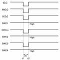
도 3은 제1 전류 싱크부(603)가 제2 전압을 센싱하기 위한 파형도이고, 도 4는 제2 전류 싱크부(605)가 제3 전압을 센싱하기 위한 파형도이다. 도 5는 전류 소스부(601)가 제1 전압을 센싱하기 위한 파형도이며, 도 6은 데이터 신호가 전달되어 화소(100)에서 영상이 표시되기 위한 파형도이다.3 is a waveform diagram for sensing the second voltage by the first
상기 도 3 내지 도 6의 파형도는 도 2에 제시된 화소(100)의 회로를 구성하는 트랜지스터들 및 복수의 선택 스위치들이 PMOS인 것을 상정하여 제안한 것이며, 만일 화소(100)의 회로에 포함되는 트랜지스터들 및 복수의 선택 스위치들이 NMOS로 구현된다면 파형도의 극성이 반전될 것이다.The waveform diagrams of FIGS. 3 to 6 are proposed assuming that the transistors and the plurality of selection switches constituting the circuit of the
도 3의 파형도에 따라 화소(100)의 구동 트랜지스터(M1)의 게이트 전극에 걸리는 전압이 센싱되는 과정은 다음과 같다.According to the waveform diagram of FIG. 3, the voltage applied to the gate electrode of the driving transistor M1 of the
시점(t1)에서 화소(100)에 대응하는 데이터선에 접속된 데이터 선택 스위치(SW1)를 제어하는 데이터 선택 신호(SWC1)가 하이 레벨로 전달되어 데이터 선택 스위치(SW1)가 턴 오프 된다. 반면, 화소(100)에 대응하는 데이터선으로부터 분기된 보상선(73)에 접속된 보상부 선택 스위치(SWm)는 이를 제어하는 보상부 선택 신호(SWCm)가 시점(t1)에서 로우 레벨로 전달되므로 턴 온 된다.At a time point t1, the data selection signal SWC1 for controlling the data selection switch SW1 connected to the data line corresponding to the
시점(t1)에서 화소(100)에 공급되는 주사 신호(S[n]), 발광 제어 신호(EM[n]), 및 감지 신호(SE[n]) 각각이 로우 레벨 전압으로 전달된다. 이로 인해 화소(100) 내에서 주사 신호(S[n])를 전달받은 제2 트랜지스터(M2), 발광 제어 신호(EM[n])를 전달받은 제3 트랜지스터(M4), 및 감지 신호(SE[n])를 전달받은 제1 트랜지스터(M3)가 시점(t1)에서 턴 온 된다.At the time point t1, the scan signal S [n], the emission control signal EM [n], and the sensing signal SE [n] supplied to the
제2 트랜지스터(M2), 제3 트랜지스터(M4), 및 제1 트랜지스터(M3)가 턴 온 되는 기간(P1) 동안, 제1 전류 싱크부(603)의 제2 스위치(SW3)는 로우 레벨의 선택 신호(SWC3)에 의해 턴 온 된다. 그러면 제2 전류가 이 기간 동안 턴 온 된 보상부 선택 스위치(SWm)를 통해 연결된 데이터선을 통해 싱크된다.During the period P1 in which the second transistor M2, the third transistor M4, and the first transistor M3 are turned on, the second switch SW3 of the first
따라서, 구동 트랜지스터(M1)가 턴 온 되어 제1 전원 전압(ELVDD)부터 유기 발광 다이오드(OLED)의 캐소드 전극까지 전류 경로가 형성된다. 또한 구동 트랜지스터(M1)의 게이트 전극과 제1 전극의 전압차(Vgs)는 제2 전류에 대응하는 전압값으로 형성되며 그에 따라 구동 트랜지스터(M1)의 게이트 전극의 전압(제2 전압)이 제1 노드(N1)에 인가된다.Accordingly, the driving transistor M1 is turned on to form a current path from the first power supply voltage ELVDD to the cathode electrode of the organic light emitting diode OLED. In addition, the voltage difference Vgs between the gate electrode and the first electrode of the driving transistor M1 is formed at a voltage value corresponding to the second current, and accordingly, the voltage (second voltage) of the gate electrode of the driving transistor M1 is set to zero. It is applied to one node N1.
상기 제2 전압은 제2 트랜지스터(M2)를 통해 화소(100)에 연결된 데이터선(Dm)을 경유하여 ADC(607)로 전달되어 디지털 값으로 변환된다.The second voltage is transferred to the
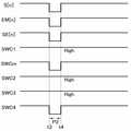
도 4를 참조하면, 시점(t3) 에서 시점(t4)까지 데이터 선택 스위치(SW1)를 제어하는 데이터 선택 신호(SWC1)가 하이 레벨로 전달되어 데이터 선택 스위치(SW1)가 턴 오프 된다. 반면, 화소(100)에 대응하는 데이터선으로부터 분기된 보상선(73)에 접속된 보상부 선택 스위치(SWm)는 이를 제어하는 보상부 선택 신호(SWCm)가 시점(t3)에서 로우 레벨로 전달되므로 턴 온 된다.Referring to FIG. 4, the data select signal SWC1 controlling the data select switch SW1 is transferred to a high level from the time point t3 to the time point t4, so that the data select switch SW1 is turned off. On the other hand, the compensator selector switch SWm connected to the
시점(t3) 에서 화소(100)에 공급되는 주사 신호(S[n]), 발광 제어 신호(EM[n]), 및 감지 신호(SE[n]) 각각이 로우 레벨 전압으로 전달되어, 제2 트랜지스터(M2), 제3 트랜지스터(M4), 및 제1 트랜지스터(M3)를 각각 기간(P2) 동안 턴 온 시킨다.The scan signal S [n], the emission control signal EM [n], and the sensing signal SE [n] supplied to the
이 때 제2 전류 싱크부(605)의 제3 스위치(SW4)는 로우 레벨의 선택 신호(SWC4)에 응답하여 턴 온 된다. 그러면 제2 전류 싱크부(605)가 기간(P2) 동안 턴 온 된 보상부 선택 스위치(SWm)를 통해 연결된 데이터선을 통해 제3 전류를 싱크한다.In this case, the third switch SW4 of the second
따라서, 구동 트랜지스터(M1)가 턴 온 되어 제1 전원 전압(ELVDD)부터 유기 발광 다이오드(OLED)의 캐소드 전극까지 전류 경로가 형성된다. 또한 구동 트랜지스터(M1)의 게이트 전극과 제1 전극의 전압차(Vgs)는 제3 전류에 대응하는 전압값으로 형성되며 그에 따라 구동 트랜지스터(M1)의 게이트 전극의 전압(제3 전압)이 제1 노드(N1)에 인가된다.Accordingly, the driving transistor M1 is turned on to form a current path from the first power supply voltage ELVDD to the cathode electrode of the organic light emitting diode OLED. In addition, the voltage difference Vgs between the gate electrode and the first electrode of the driving transistor M1 is formed at a voltage value corresponding to the third current, and accordingly, the voltage (third voltage) of the gate electrode of the driving transistor M1 is set to the third voltage. It is applied to one node N1.
상기 제3 전압은 제2 트랜지스터(M2)를 통해 화소(100)에 연결된 데이터선(Dm)을 경유하여 ADC(607)로 전달되어 디지털 값으로 변환된다.The third voltage is transferred to the
보상부(60)의 메모리부(609)는상기 변환된 제2 전압 및 제3 전압의디지털 값을 각각 저장하고, 제어부(613)는 이들 전압값으로부터 화소(100)의 구동 트랜지스터(M1)의 문턱 전압과 전자 이동도를 산출해낸다.The
도 5의 파형도는 화소(100)의 유기 발광 다이오드(OLED)의 구동 전압이 센싱되는 기간의 파형도이다.5 is a waveform diagram of a period in which a driving voltage of the organic light emitting diode OLED of the
시점(t5)부터 시점(t6)까지의 기간(P3) 동안 데이터 선택 신호(SWC1)가 하이 레벨로 전달되어 데이터 선택 스위치(SW1)가 턴 오프 되고, 보상부 선택 신호(SWCm)가 로우 레벨이므로 화소(100)에 대응하는 데이터선으로부터 분기된 보상선(73)에 접속된 보상부 선택 스위치(SWm)가 턴 온 된다.Since the data select signal SWC1 is transferred to the high level during the period P3 from the time point t5 to the time point t6, the data select switch SW1 is turned off and the compensator select signal SWCm is low. The compensation part select switch SWm connected to the
기간(P3) 동안, 주사 신호(S[n]) 및 발광 제어 신호(EM[n])는 하이 레벨 전압으로 전달되고, 감지 신호(SE[n])는 로우 레벨 전압으로 전달된다.During the period P3, the scan signal S [n] and the emission control signal EM [n] are transmitted at the high level voltage, and the sense signal SE [n] is transferred at the low level voltage.
따라서, 화소(100) 내에서 주사 신호(S[n])를 전달받은 제2 트랜지스터(M2) 및 발광 제어 신호(EM[n])를 전달받은 제3 트랜지스터(M4)는 기간(P3) 동안 턴 오프 되고, 감지 신호(SE[n])를 전달받은 제1 트랜지스터(M3)는 기간(P3) 동안 턴 온 된다.Therefore, in the
이 때 전류 소스부(601)의 제1 스위치(SW2)는 로우 레벨의 선택 신호(SWC2)를 전달받아 그에 응답하여 턴 온 된다. 그러면 전류 소스부(601)가 기간(P3) 동안 턴 온 된 보상부 선택 스위치(SWm)를 통해 연결된 데이터선으로 제1 전류를 유기 발광 다이오드(OLED)에 공급한다.At this time, the first switch SW2 of the
정상적인 유기 발광 다이오드(OLED)의 경우 애노드 전극에 인가되는 구동 전압은 제1 전류에 대응하는 적절한 전압값이 될 것이지만, 열화된 유기 발광 다이오드(OLED)는 저항이 증가하여 유기 발광 다이오드(OLED)의 애노드 전극에 인가되는 구동 전압이 상대적으로 증가된다. 이렇게 증가된 유기 발광 다이오드(OLED)의 구동 전압은 제1 전압이고, 제1 전압이 턴 온 된 제1 트랜지스터(M3)를 통해 데이터선을 거쳐 ADC(607)로 전달되어 디지털 값으로 변환된다.In the case of a normal organic light emitting diode (OLED), the driving voltage applied to the anode electrode will be an appropriate voltage value corresponding to the first current. The driving voltage applied to the anode electrode is relatively increased. The increased driving voltage of the OLED is a first voltage, and the first voltage is transferred to the
메모리부(609)는 상기 변환된 제1 전압의 디지털 값을 저장하고, 제어부(613)는 유기 발광 다이오드(OLED)가 데이터 신호에 따른 적절한 휘도로 발광할 수 있도록 제1 전압을 기초로 하여 열화에 의해 증가된 전압값만큼 보상하는 데이터 신호 보상량을 결정한다.The
도 6은 화소(100)가 정상적으로 데이터 신호에 따라 발광하기 위한 파형도를 나타낸다.6 shows a waveform diagram for the
시점(t7) 내지 시점(t8)의 기간 동안 화소(100)에 대응하는 데이터선에 접속된 데이터 선택 스위치(SW1)는 데이터 선택 신호(SWC1)가 로우 레벨이므로 이에 응답하여 턴 온 된다. 반면, 화소(100)에 대응하는 데이터선으로부터 분기된 보상선(73)에 접속된 보상부 선택 스위치(SWm)는 이를 제어하는 보상부 선택 신호(SWCm)가 시점(t7) 내지 시점(t8)의 기간 동안 하이 레벨로 전달되므로 턴 오프 된다.The data select switch SW1 connected to the data line corresponding to the
시점(t7)에서 화소(100)에 공급되는 주사 신호(S[n])가 로우 레벨 전압으로 공급되고, 제2 트랜지스터(M2)는 기간(P4) 동안 턴 온 된다.At a time point t7, the scan signal S [n] supplied to the
기간(P4) 동안 상기 턴 온 된 데이터 선택 스위치(SW1)를 통해 데이터 구동부(30)는 대응하는 데이터선(Dm)으로 보상된 데이터 신호를 전달한다. 데이터 신호는 제2 트랜지스터(M2)를 거쳐 제1 노드(N1)에 전달되는데, 제1 노드(N1)에 연결된 스토리지 커패시터(Cst)는 데이터 신호에 대응하는 전압값을 충전한다.During the period P4, the
타이밍 제어부(50)는 보상부(60)로부터 화소(100)의 유기 발광 다이오드(OLED)의 열화에 따른 보상량 또는 구동 트랜지스터(M1)의 문턱 전압과 이동도 편차 및 이동도 변화를 보상하는 보상량을 전달받고 외부에서 공급된 영상 데이터 신호(Data1)의 비트수를 증가하여 보정된 영상 데이터 신호(Data2)를 생성한다.The
도 7은 도 1에 도시된 화소의 다른 일 실시 예에 의한 회로도이고, 상기 화소로 공급되는 신호의 구동 파형을 도 8에 나타내었다.FIG. 7 is a circuit diagram according to another exemplary embodiment of the pixel illustrated in FIG. 1, and a driving waveform of a signal supplied to the pixel is illustrated in FIG. 8.
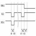
도 7의 화소의 구성은 도 2의 화소의 구성과 크게 다르지 않으므로 차이점을 중심으로 기술하기로 한다.Since the configuration of the pixel of FIG. 7 is not significantly different from the configuration of the pixel of FIG. 2, the difference will be described.
도 7을 참조하면 화소(100)는 유기 발광 다이오드(Organic Light Emitting Diode, OLED), 구동 트랜지스터(M1), 제1 트랜지스터(M3), 제2 트랜지스터(M2), 제3 트랜지스터(M4), 제4 트랜지스터(M5) 및 스토리지 커패시터(Cst)를 포함한다.Referring to FIG. 7, the
도 2의 화소와 비교하여 n 번째 발광 제어선(EMn)을 통해 대응하는발광 제어 신호를 전달받는 제3 트랜지스터(M4)가 노드 A 및 구동 트랜지스터(M1)의 제2 전극과 제1 전원 전압(ELVDD)이 접속되는 접점 사이에 연결되어 있다.Compared to the pixel of FIG. 2, the third transistor M4, which receives the corresponding emission control signal through the nth emission control line EMn, receives the second electrode and the first power supply voltage of the node A and the driving transistor M1. ELVDD) is connected between the contacts to be connected.
구체적으로 제3 트랜지스터(M4)의 게이트 전극은 복수의 발광 제어선 중 대응하는 발광 제어선(EMn)에 접속되고, 제1 전극은 구동 트랜지스터(M1)의 제2 전극에 접속되며, 제2 전극은 노드(A)에 접속된다. 제3 트랜지스터(M4)는 발광 제어선(EMn)으로 게이트 온 전압 레벨을 가지는 발광 제어 신호가 공급되면 턴 온 되고 그 외의 경우에는 턴 오프 된다. 발광 제어 신호는 데이터선(Dm)으로부터 소정의 데이터 신호가 전달되는 기간, 즉 데이터가 기입되는 기간 후에 게이트 온 전압 레벨로 전달된다. 그러면 구동 트랜지스터(M1)를 통해 스토리지 커패시터(Cst)에 충전된 데이터 전압에 따른 구동 전류가 유기 발광 다이오드(OLED)에 공급되어 영상이 표시된다.Specifically, the gate electrode of the third transistor M4 is connected to the corresponding emission control line EMn of the plurality of emission control lines, the first electrode is connected to the second electrode of the driving transistor M1, and the second electrode Is connected to node (A). The third transistor M4 is turned on when the emission control signal having the gate-on voltage level is supplied to the emission control line EMn, and is otherwise turned off. The emission control signal is transmitted at the gate-on voltage level after a period in which a predetermined data signal is transmitted from the data line Dm, that is, a period in which data is written. Then, a driving current corresponding to the data voltage charged in the storage capacitor Cst through the driving transistor M1 is supplied to the organic light emitting diode OLED to display an image.
스토리지 커패시터(Cst)는 일단이 구동 트랜지스터(M1)의 게이트 전극에 접속되고 타단이 구동 트랜지스터(M1)의 제1 전극 및 제1 전원 전압(ELVDD)에 접속되어 있다.One end of the storage capacitor Cst is connected to the gate electrode of the driving transistor M1, and the other end thereof is connected to the first electrode and the first power supply voltage ELVDD of the driving transistor M1.
스토리지 커패시터(Cst)는 구동 트랜지스터(M1)의 문턱 전압에 대응하는 전압이 충전한다. 데이터선(Dm)으로부터 데이터 신호가 전달되면 스토리지 커패시터(Cst)의 일단과 구동 트랜지스터(M1)의 게이트 전극이 연결되어 있는 제1 노드(N1)에 걸리는 전압은 상기 데이터 신호에 대응하여 변한다. 이 때 스토리지 커패시터(Cst)는 데이터선(Dm)으로부터 전달된 상기 데이터 신호에 대응하는 전압만큼 저장한다.The storage capacitor Cst is charged with a voltage corresponding to the threshold voltage of the driving transistor M1. When the data signal is transferred from the data line Dm, the voltage across the first node N1, which is connected to one end of the storage capacitor Cst and the gate electrode of the driving transistor M1, changes in response to the data signal. In this case, the storage capacitor Cst stores the voltage corresponding to the data signal transferred from the data line Dm.
스토리지 커패시터(Cst)의 타단은 노드(A)에 연결되어 있는데, 노드(A)와 보조 전원(Vsus) 사이에 제4 트랜지스터(M5)가 위치한다.The other end of the storage capacitor Cst is connected to the node A. The fourth transistor M5 is positioned between the node A and the auxiliary power supply Vsus.
구체적으로 제4 트랜지스터(M5)의 게이트 전극은 복수의 주사선 중 대응하는 주사선(Sn)에 접속되고, 제1 전극은 보조 전원(Vsus)에 접속되며 제2 전극은 노드(A)에 접속된다.Specifically, the gate electrode of the fourth transistor M5 is connected to the corresponding scan line Sn of the plurality of scan lines, the first electrode is connected to the auxiliary power supply Vsus, and the second electrode is connected to the node A.
제4 트랜지스터(M5)는 주사선(Sn)을 통해 전달되는 게이트 온 전압 레벨의 주사 신호에 응답하여 턴 온 되고, 그 외의 경우에는 턴 오프 된다. 온 전압 레벨의 주사 신호는 보상부(60)에서 구동 트랜지스터(M1)의 게이트 전극에 걸리는 전압과 유기 발광 다이오드(OLED)의 구동 전압이 센싱되는 기간, 및 데이터선(Dm)으로부터 소정의 데이터 신호가 전달되는 기간 동안 공급된다.The fourth transistor M5 is turned on in response to a scan signal having a gate-on voltage level transmitted through the scan line Sn, and is otherwise turned off. The scan signal of the on voltage level is a period in which the voltage applied to the gate electrode of the driving transistor M1 and the driving voltage of the organic light emitting diode OLED are sensed by the
그러면 제4 트랜지스터(M5)가 상기 주사 신호에 대응하여 턴 온 되어 노드(A)로 보조 전원(Vsus)의 보조 전압을 전달한다. 보조 전압은 제1 전원 전압(ELVDD)의 IR drop 현상에 따라 강하되는 전압값을 보상할 수 있다.Then, the fourth transistor M5 is turned on in response to the scan signal to transmit the auxiliary voltage of the auxiliary power supply Vsus to the node A. The auxiliary voltage may compensate for the voltage value dropped by the IR drop phenomenon of the first power voltage ELVDD.
도 7의 화소(100) 회로도를 참조하여 도 8의 파형도에 따라 영상 데이터 신호의 보상을 위해 유기 발광 다이오드(OLED)의 구동 전압 혹은 구동 트랜지스터(M1)의 게이트 전극 전압이 검출되고, 화소가 발광하는 과정을 설명한다.Referring to the circuit diagram of the
시점(t9)에서 화소(100)에 공급되는 주사 신호(S[n]) 및 감지 신호(SE[n]) 각각이 로우 레벨 전압으로 전달된다. 이로 인해 화소(100) 내에서 주사 신호(S[n])를 전달받은 제2 트랜지스터(M2)와 제4 트랜지스터(M5), 및 감지 신호(SE[n])를 전달받은 제1 트랜지스터(M3)가 시점(t9)에서 시점(t10)에 이르기까지 기간(P5) 동안 턴 온 된다.At a time point t9, each of the scan signal S [n] and the sense signal SE [n] supplied to the
그러면 보상부(60)로부터 소정의 전류가 싱크되어 구동 트랜지스터(M1)의 게이트 전극과 제1 전극의 전압차(Vgs)는 소정의 전류에 대응하는 전압값으로 형성되며 그에 따라 구동 트랜지스터(M1)의 게이트 전극의 전압이 제1 노드(N1)에 인가된다. 상기 전압은 화소(100)에 연결된 데이터선(Dm)을 경유하여 보상부(60)로 전달된다. 이에 따라 구동 트랜지스터(M1)의 문턱 전압과 이동도가 산출되고 보상량이 결정되는 것은 상술한 바와 같다.Then, a predetermined current is sinked from the
도 8에는 도시하지 않았으나 이미지 스틱킹을 보상하기 위해 화소(100)의 유기 발광 다이오드(OLED)의 구동 전압이 검출되는 동안의 파형은 상술한 바와 같으므로 구체적인 설명은 생략한다.Although not shown in FIG. 8, the waveform while the driving voltage of the organic light emitting diode OLED of the
보상을 위한 전압의 센싱 과정 이후에 시점(t11)에서는 화소(100)에 공급되는 제어 신호들 중 주사 신호(S[n])만이 로우 레벨로 인가되어 제2 트랜지스터(M2)와 제4 트랜지스터(M5)를 기간(P6) 동안 턴 온 시킨다.After the process of sensing the voltage for compensation, at time t11, only the scan signal S [n] among the control signals supplied to the
기간(P6) 동안 구동 트랜지스터(M1) 역시 턴 온 되며, 대응하는 데이터선(Dm)으로부터 소정의 보상된 데이터 신호가 전달된다. 상기 데이터 신호에 따른 데이터 전압만큼 스토리지 커패시터(Cst)에 충전되고 안정적인 제1 전원 전압(ELVDD)의 공급 전압을 유지하기 위해 제4 트랜지스터(M5)를 통해 보조 전압이 스토리지 커패시터(Cst)의 타단에 인가된다.The driving transistor M1 is also turned on during the period P6, and a predetermined compensated data signal is transferred from the corresponding data line Dm. An auxiliary voltage is applied to the other end of the storage capacitor Cst through the fourth transistor M5 to maintain the supply voltage of the first power supply voltage ELVDD that is charged and stable to the storage capacitor Cst by the data voltage according to the data signal. Is approved.
다음으로 시점(t12)에서 대응하는 주사 신호(S[n])가 하이 레벨로 상승하고 대응하는 발광 제어 신호(EM[n])가 로우 레벨 전압으로 전달된다.Next, at time t12, the corresponding scan signal S [n] rises to a high level and the corresponding emission control signal EM [n] is transferred to a low level voltage.
이로 인해 제2 트랜지스터(M2)와 제4 트랜지스터(M5)는 턴 오프 되고, 제3 트랜지스터(M4)가 기간(P7) 동안 턴 온 되어 스토리지 커패시터(Cst)에 저장된 데이터 신호에 따른 전압에 대응하는 구동 전류가 유기 발광 다이오드(OLED)에 전달되어 유기 발광 다이오드(OLED)가 발광한다.As a result, the second transistor M2 and the fourth transistor M5 are turned off, and the third transistor M4 is turned on for the period P7 to correspond to the voltage according to the data signal stored in the storage capacitor Cst. The driving current is transmitted to the organic light emitting diode OLED so that the organic light emitting diode OLED emits light.
도 9는 본 발명의 일 실시 예에 따른 유기 발광 표시 장치의 계조별 전류 곡선을 나타내는 그래프이다.9 is a graph illustrating a current curve for each gray level of an organic light emitting diode display according to an exemplary embodiment.
도 9의 그래프는 유기 발광 표시 장치에서 이미지 스틱킹 보상 및 균일 휘도를 위한 보상을 수행하고 이동도 불균일에 의한 편차를 보정하여 데이터 전압에 대한 오차를 제거한 결과를 나타내었다.The graph of FIG. 9 illustrates a result of eliminating an error in data voltage by performing image sticking compensation and compensation for uniform brightness and correcting a deviation due to mobility unevenness in the OLED display.
도 9를 참조하면 본 발명의 일 실시 예에 따른 방법으로 영상 데이터 신호를 보정한 데이터 신호에 따라 발광하는 화소 영상의 계조별 전류 곡선은 2.2 감마 곡선에 일치하여 저계조 데이터 영역까지 충분히 표현되고 있음을 알 수 있다.Referring to FIG. 9, a current curve for each gray level of a pixel image that emits light according to a data signal corrected by the method according to an exemplary embodiment of the present invention is sufficiently represented by a low gray scale data region in accordance with a 2.2 gamma curve. It can be seen.
이상 본 발명의 구체적 실시형태와 관련하여 본 발명을 설명하였으나 이는 예시에 불과하며 본 발명은 이에 제한되지 않는다. 당업자는 본 발명의 범위를 벗어나지 않고 설명된 실시형태를 변경 또는 변형할 수 있으며, 이러한 변경 또는 변형도 본 발명의 범위에 속한다. 또한, 명세서에서 설명한 각 구성요소의 물질은 당업자가 공지된 다양한 물질로부터 용이하게 선택하여 대체할 수 있다. 또한 당업자는 본 명세서에서 설명된 구성요소 중 일부를 성능의 열화 없이 생략하거나 성능을 개선하기 위해 구성요소를 추가할 수 있다. 뿐만 아니라, 당업자는 공정 환경이나 장비에 따라 본 명세서에서 설명한 방법 단계의 순서를 변경할 수도 있다. 따라서 본 발명의 범위는 설명된 실시형태가 아니라 특허청구범위 및 그 균등물에 의해 결정되어야 한다.The present invention has been described above in connection with specific embodiments of the present invention, but this is only an example and the present invention is not limited thereto. Those skilled in the art can change or modify the described embodiments without departing from the scope of the present invention, and such changes or modifications are within the scope of the present invention. In addition, the materials of each component described in the specification can be easily selected and replaced by a variety of materials known to those skilled in the art. Those skilled in the art will also appreciate that some of the components described herein can be omitted without degrading performance or adding components to improve performance. In addition, those skilled in the art may change the order of the method steps described herein depending on the process environment or equipment. Therefore, the scope of the present invention should be determined by the appended claims and equivalents thereof, not by the embodiments described.
10: 표시부20: 주사 구동부
30: 데이터 구동부31: 디지털 아날로그 변환부
33: 연산 증폭기40: 감지 구동부
50: 타이밍 제어부60: 보상부
70: 선택부73: 보상 라인
75: 선택 구동부100: 화소
601: 전류 소스부603: 제1 전류 싱크부
605: 제2 전류 싱크부607: ADC
609: 메모리부611: 룩업 테이블
613: 제어부10: display unit 20: scan driver
30: data driver 31: digital-to-analog converter
33: operational amplifier 40: sense driver
50: timing controller 60: compensator
70: selection unit 73: compensation line
75: selective driving unit 100: pixel
601: current source unit 603: first current sink unit
605: second current sink 607: ADC
609: Memory 611: Lookup Table
613: control unit
Claims (21)
Translated fromKorean상기 복수의 화소 각각에 연결된 데이터선을 통해, 유기 발광 다이오드에 이르는 구동 전류의 경로로 소정의 전류를 싱크하는 동안 상기 복수의 구동 트랜지스터 각각의 게이트 전극에 인가되는 소정의 전압을 전달받아 상기 복수의 구동 트랜지스터 각각의 문턱 전압, 이동도 및 이동도의 변화를 구하여 입력 영상 데이터 신호에 따른 보상량 및 감마를 결정하는 보상부;
상기 보상량 및 감마를 전달받아 입력 영상 데이터 신호에 보상량을 더하고 상기 결정된 감마에 따라 보정된 영상 데이터 신호를 생성하는 타이밍 제어부; 및
상기 보정된 영상 데이터 신호에 기초하여 데이터 전압을 생성하고, 상기 복수의 화소에 상기 데이터 전압을 공급하는 데이터 구동부를 포함하고,
상기 보상부는 상기 구동 트랜지스터의 이동도 변화에 따른 감마 변화 데이터를 포함하는 룩업테이블을 포함하고 상기 룩업테이블을 이용하여 상기 이동도 변화에 따른 감마를 결정하는 유기 발광 표시 장치.A plurality of pixels including a plurality of organic light emitting diodes and a plurality of driving transistors respectively supplying a driving current to each of the plurality of organic light emitting diodes;
The plurality of driving transistors receive a predetermined voltage applied to a gate electrode of each of the plurality of driving transistors while sinking a predetermined current through a data line connected to each of the plurality of pixels through a path of driving current to the organic light emitting diode. A compensator for determining a compensation amount and a gamma according to the input image data signal by obtaining a change in threshold voltage, mobility, and mobility of each driving transistor;
A timing controller configured to receive the compensation amount and gamma, add a compensation amount to an input image data signal, and generate a corrected image data signal according to the determined gamma; And
A data driver configured to generate a data voltage based on the corrected image data signal and supply the data voltage to the plurality of pixels;
The compensator includes a lookup table including gamma change data according to a change in mobility of the driving transistor, and determines a gamma according to the change in mobility using the lookup table.
상기 보상부는,
상기 소정의 전류를 싱크하는 적어도 하나 이상의 전류 싱크부;
상기 문턱 전압, 이동도 및 이동도의 편차를 구하고 상기 보상량을 결정하는 제어부; 및
상기 소정의 전압을 전달받아 저장하고, 상기 결정된 보상량을 저장하는 메모리부를 더 포함하는 유기 발광 표시 장치.The method of claim 1,
The compensation unit,
At least one current sink for sinking the predetermined current;
A controller configured to obtain a deviation of the threshold voltage, mobility, and mobility and determine the compensation amount; And
And a memory unit configured to receive and store the predetermined voltage and store the determined compensation amount.
상기 전류 싱크부는,
소정의 제1 전류를 싱크하는 제1 전류 싱크부 및 상기 제1 전류보다 전류값이 낮은 제2 전류를 싱크하는 제2 전류 싱크부인 유기 발광 표시 장치.The method of claim 2,
The current sink unit,
An organic light emitting display device comprising: a first current sinker for sinking a predetermined first current; and a second current sinker for sinking a second current having a lower current value than the first current.
상기 제1 전류는 유기 발광 다이오드가 최대 휘도로 발광할 때 상기 유기 발광 다이오드에 흐르는 전류값인 유기 발광 표시 장치.The method of claim 3, wherein
And the first current is a current value flowing through the organic light emitting diode when the organic light emitting diode emits light at the maximum luminance.
상기 제1 전류 및 상기 제2 전류를 싱크하는 동안, 복수의 구동 트랜지스터 각각의 게이트 전극에 제1 전압 및 제2 전압이 인가되고,
상기 제1 전압 및 제2 전압으로부터 상기 복수의 구동 트랜지스터 각각의 문턱 전압 및 이동도가 산출되는 유기 발광 표시 장치.The method of claim 3, wherein
While sinking the first current and the second current, a first voltage and a second voltage are applied to gate electrodes of each of the plurality of driving transistors,
And a threshold voltage and a mobility of each of the plurality of driving transistors are calculated from the first voltage and the second voltage.
상기 보상부는,
상기 복수의 화소 각각에 연결된 데이터선을 통해 상기 복수의 유기 발광 다이오드 각각에 소정의 제3 전류를 공급하는 동안 상기 복수의 유기 발광 다이오드 각각의 구동 전압을 대응하는 데이터선을 통해 전달받고,
상기 전달받은 구동 전압에 따라 상기 복수의 유기 발광 다이오드 각각의 열화 정도에 따른 보상량을 결정하는 유기 발광 표시 장치.The method of claim 1,
The compensation unit,
Receiving a driving voltage of each of the plurality of organic light emitting diodes through a corresponding data line while supplying a predetermined third current to each of the plurality of organic light emitting diodes through a data line connected to each of the plurality of pixels,
And an amount of compensation according to a deterioration degree of each of the plurality of organic light emitting diodes according to the received driving voltage.
상기 보상량은 상기 복수의 유기 발광 다이오드 각각의 열화로 인해 증가된 구동 전압에 대응하는 전압값인 유기 발광 표시 장치.The method according to claim 6,
The compensation amount is a voltage value corresponding to an increased driving voltage due to deterioration of each of the plurality of organic light emitting diodes.
상기 보상부는,
상기 제3 전류를 공급하는 전류 소스부를 더 포함하는 유기 발광 표시 장치.The method according to claim 6,
The compensation unit,
And a current source unit configured to supply the third current.
상기 유기 발광 표시 장치는 상기 보상부와 데이터 구동부 및 상기 복수의 화소 사이에 선택부를 더 포함하고,
상기 선택부는,
상기 복수의 화소 각각에 연결된 데이터선에 접속되는 복수의 데이터 선택 스위치;
상기 복수의 데이터선 각각에서 분기된 복수의 보상선의 접점에 접속되는 복수의 보상부 선택 스위치; 및
상기 복수의 데이터 선택 스위치 및 복수의 보상부 선택 스위치 각각의 스위칭 동작을 제어하는 복수의 선택 신호를 생성하여 전달하는 선택 구동부를 포함하는 유기 발광 표시 장치.The method of claim 1,
The organic light emitting diode display further includes a selector between the compensator, the data driver, and the plurality of pixels.
The selection unit,
A plurality of data selection switches connected to data lines connected to each of the plurality of pixels;
A plurality of compensation part selection switches connected to the contacts of the plurality of compensation lines branched from each of the plurality of data lines; And
And a selection driver configured to generate and transmit a plurality of selection signals for controlling switching operations of each of the plurality of data selection switches and the plurality of compensation unit selection switches.
상기 복수의 화소 각각은,
상기 복수의 유기 발광 다이오드 각각의 일 전극과 상기 복수의 화소 각각에 연결된 데이터선 사이에 위치하는 복수의 제1 트랜지스터; 및
상기 복수의 화소 각각에 연결된 데이터선과 상기 복수의 구동 트랜지스터 각각의 게이트 전극 사이에 위치하는 복수의 제2 트랜지스터를 더 포함하는 유기 발광 표시 장치.The method of claim 1,
Each of the plurality of pixels,
A plurality of first transistors positioned between one electrode of each of the plurality of organic light emitting diodes and a data line connected to each of the plurality of pixels; And
And a plurality of second transistors disposed between the data lines connected to each of the plurality of pixels and the gate electrodes of each of the plurality of driving transistors.
상기 복수의 제1 트랜지스터 및 복수의 제2 트랜지스터 각각이 턴 온 되는 동안, 소정의 전류를 싱크하고 상기 복수의 구동 트랜지스터 각각의 게이트 전극에 인가되는 소정의 전압이 보상부에 전달되는 유기 발광 표시 장치.The method of claim 10,
While each of the plurality of first transistors and the plurality of second transistors is turned on, the organic light emitting diode display is configured to sink a predetermined current and transfer a predetermined voltage applied to a gate electrode of each of the plurality of driving transistors to a compensation unit. .
상기 복수의 제1 트랜지스터 각각이 턴 온 되고, 상기 복수의 제2 트랜지스터 각각이 턴 오프 되는 동안, 소정의 전류를 공급하고 상기 복수의 유기 발광 다이오드 각각의 구동 전압이 보상부에 전달되는 유기 발광 표시 장치.The method of claim 10,
While each of the plurality of first transistors is turned on and each of the plurality of second transistors is turned off, an organic light emitting display in which a predetermined current is supplied and a driving voltage of each of the plurality of organic light emitting diodes is transferred to a compensator. Device.
상기 타이밍 제어부는 수학식

를 이용하여 상기 보정된 영상 데이터 신호를 생성하고, 상기 VDATA는 상기 보정된 영상 데이터 신호에 따른 데이터 전압이고, 상기 ELVDD는 제1 전원 전압이고, 상기 data는 상기 입력 영상 데이터 신호이고, 상기 β는 상기 구동 트랜지스터의 이동도이고, 상기

The timing control unit is
Generate the corrected image data signal by using the VDATA , the VDATA is a data voltage according to the corrected image data signal, the ELVDD is a first power supply voltage, the data is the input image data signal, and Is the mobility of the driving transistor,
상기 소정의 전압을 이용하여 상기 복수의 구동 트랜지스터 각각의 문턱 전압, 이동도 및 상기 이동도의 편차를 구하여 입력 영상 데이터 신호에 따른 보상량을 결정하고, 이동도의 변화에 따른 감마의 변화 데이터를 포함하는 룩업테이블을 이용하여 상기 이동도의 편차에 따른 감마를 결정하는 단계; 및
상기 보상량을 입력 영상 데이터 신호에 더하고 상기 결정된 감마에 따라 보정된 영상 데이터 신호를 생성하고, 상기 보정된 영상 데이터 신호에 따른 데이터 전압을 생성하여 복수의 화소 각각에 전달하는 단계를 포함하는 유기 발광 표시 장치의 구동 방법.A gate electrode of each of the plurality of driving transistors while a predetermined current is sinked through a data line corresponding to each of the plurality of pixels through a driving transistor included in each of the plurality of pixels via a driving current to the organic light emitting diode Receiving a predetermined voltage applied to the;
The threshold voltage, mobility, and deviation of the mobility of each of the plurality of driving transistors are obtained using the predetermined voltage to determine a compensation amount according to an input image data signal, and change data of gamma according to the change of mobility. Determining a gamma according to the deviation of the mobility using a lookup table that includes; And
Adding the compensation amount to an input image data signal, generating a corrected image data signal according to the determined gamma, and generating and transmitting a data voltage according to the corrected image data signal to each of the plurality of pixels. Method of driving the display device.
상기 소정의 전압을 전달받는 단계는,
제1 전류를 싱크하고, 상기 복수의 구동 트랜지스터 각각의 게이트 전극에 인가되는 제1 전압을 전달받는 단계; 및
상기 제1 전류보다 전류값이 낮은 제2 전류를 싱크하고, 상기 복수의 구동 트랜지스터 각각의 게이트 전극에 인가되는 제2 전압을 전달받는 단계를 포함하는 유기 발광 표시 장치의 구동 방법.The method of claim 14,
Receiving the predetermined voltage,
Sinking a first current and receiving a first voltage applied to a gate electrode of each of the plurality of driving transistors; And
And sinking a second current having a current value lower than the first current and receiving a second voltage applied to a gate electrode of each of the plurality of driving transistors.
상기 제1 전류는 유기 발광 다이오드가 최대 휘도로 발광할 때 상기 유기 발광 다이오드에 흐르는 전류값인 유기 발광 표시 장치의 구동 방법.16. The method of claim 15,
And wherein the first current is a current value flowing through the organic light emitting diode when the organic light emitting diode emits light at the maximum luminance.
상기 소정의 전압을 전달받는 단계 이전 또는 이후에,
복수의 화소 각각에 대응하는 데이터선을 통해 상기 복수의 화소 각각에 포함되는 복수의 유기 발광 다이오드 각각에 소정의 제3 전류를 공급하고, 상기 복수의 유기 발광 다이오드 각각의 구동 전압을 전달받는 단계; 및
상기 전달받은 구동 전압에 따라 상기 복수의 유기 발광 다이오드 각각의 열화 정도에 따른 보상량을 결정하는 단계를 더 포함하는 유기 발광 표시 장치의 구동 방법.The method of claim 14,
Before or after the step of receiving the predetermined voltage,
Supplying a predetermined third current to each of the plurality of organic light emitting diodes included in each of the plurality of pixels through a data line corresponding to each of the plurality of pixels, and receiving a driving voltage of each of the plurality of organic light emitting diodes; And
And determining a compensation amount according to a deterioration degree of each of the plurality of organic light emitting diodes according to the received driving voltage.
상기 복수의 화소 각각에 대응하는 데이터선을 통해 소정의 전압을 전달받는 단계 및 상기 복수의 화소 각각에 보정된 영상 데이터 신호에 따른 데이터 전압을 전달하는 단계는,
상기 복수의 데이터선에 각각 접속되는 복수의 데이터 선택 스위치 및 상기 복수의 데이터선 각각에서 분기된 복수의 보상선의 접점에 접속되는 복수의 보상부 선택 스위치를 포함하는 선택부의 스위칭 동작에 의해 제어되는 유기 발광 표시 장치의 구동 방법.The method of claim 14,
Receiving a predetermined voltage through a data line corresponding to each of the plurality of pixels and transmitting a data voltage according to the corrected image data signal to each of the plurality of pixels,
Induction controlled by a switching operation of a selection unit including a plurality of data selection switches respectively connected to the plurality of data lines and a plurality of compensation unit selection switches connected to contacts of a plurality of compensation lines branched from each of the plurality of data lines. A method of driving a light emitting display device.
상기 선택부는 상기 복수의 데이터 선택 스위치 및 복수의 보상부 선택 스위치 각각의 스위칭 동작을 제어하는 복수의 선택 신호를 생성하여 전달하는 선택 구동부를 더 포함하는 유기 발광 표시 장치의 구동 방법.19. The method of claim 18,
The selector further includes a selection driver configured to generate and transmit a plurality of selection signals for controlling switching operations of each of the plurality of data selection switches and the plurality of compensation unit selection switches.
상기 보정된 영상 데이터 신호는 수학식

를 이용하여 생성되고, 상기 VDATA는 상기 보정된 영상 데이터 신호에 따른 데이터 전압이고, 상기 ELVDD는 제1 전원 전압이고, 상기 data는 상기 입력 영상 데이터 신호이고, 상기 β는 상기 구동 트랜지스터의 이동도이고, 상기

The corrected image data signal is expressed by Equation
VDATA is a data voltage according to the corrected image data signal, ELVDD is a first power supply voltage, data is the input image data signal, and β is a mobility of the driving transistor. And above
Priority Applications (2)
| Application Number | Priority Date | Filing Date | Title |
|---|---|---|---|
| KR1020100018685AKR101147427B1 (en) | 2010-03-02 | 2010-03-02 | Organic light emitting display and driving method thereof |
| US12/888,115US8952951B2 (en) | 2010-03-02 | 2010-09-22 | Organic light emitting display and driving method thereof |
Applications Claiming Priority (1)
| Application Number | Priority Date | Filing Date | Title |
|---|---|---|---|
| KR1020100018685AKR101147427B1 (en) | 2010-03-02 | 2010-03-02 | Organic light emitting display and driving method thereof |
Publications (2)
| Publication Number | Publication Date |
|---|---|
| KR20110099581A KR20110099581A (en) | 2011-09-08 |
| KR101147427B1true KR101147427B1 (en) | 2012-05-22 |
Family
ID=44530933
Family Applications (1)
| Application Number | Title | Priority Date | Filing Date |
|---|---|---|---|
| KR1020100018685AActiveKR101147427B1 (en) | 2010-03-02 | 2010-03-02 | Organic light emitting display and driving method thereof |
Country Status (2)
| Country | Link |
|---|---|
| US (1) | US8952951B2 (en) |
| KR (1) | KR101147427B1 (en) |
Cited By (1)
| Publication number | Priority date | Publication date | Assignee | Title |
|---|---|---|---|---|
| CN102915702A (en)* | 2012-10-19 | 2013-02-06 | 深圳市华星光电技术有限公司 | Organic light emitting diode (OLED) display device and control method thereof |
Families Citing this family (58)
| Publication number | Priority date | Publication date | Assignee | Title |
|---|---|---|---|---|
| KR101143009B1 (en)* | 2006-01-16 | 2012-05-08 | 삼성전자주식회사 | Display device and driving method thereof |
| KR20120079354A (en)* | 2011-01-04 | 2012-07-12 | 삼성모바일디스플레이주식회사 | Shutter control system and image apparatus comprising the system |
| JP5195942B2 (en)* | 2011-01-24 | 2013-05-15 | ブラザー工業株式会社 | Scanning image display device |
| KR101536129B1 (en) | 2011-10-04 | 2015-07-14 | 엘지디스플레이 주식회사 | Organic light-emitting display device |
| KR101887238B1 (en)* | 2011-10-05 | 2018-09-10 | 엘지디스플레이 주식회사 | Organic light emitting diode displayd |
| KR101463651B1 (en) | 2011-10-12 | 2014-11-20 | 엘지디스플레이 주식회사 | Organic light-emitting display device |
| KR101493226B1 (en) | 2011-12-26 | 2015-02-17 | 엘지디스플레이 주식회사 | Method and apparatus for measuring characteristic parameter of pixel driving circuit of organic light emitting diode display device |
| KR102000041B1 (en)* | 2011-12-29 | 2019-07-16 | 엘지디스플레이 주식회사 | Method for driving light emitting display device |
| KR101615332B1 (en) | 2012-03-06 | 2016-04-26 | 삼성디스플레이 주식회사 | Pixel arrangement structure for organic light emitting display device |
| US10832616B2 (en) | 2012-03-06 | 2020-11-10 | Samsung Display Co., Ltd. | Pixel arrangement structure for organic light emitting diode display |
| CN102708819B (en)* | 2012-05-10 | 2014-08-13 | 北京京东方光电科技有限公司 | Pixel drive circuit and drive method, array substrate and display unit thereof |
| KR101917757B1 (en)* | 2012-06-04 | 2018-11-13 | 삼성전자주식회사 | Organic lighting emitting display and driving method thereof |
| KR20140014694A (en)* | 2012-07-25 | 2014-02-06 | 삼성디스플레이 주식회사 | Apparatus and method for compensating of image in display device |
| TWI570680B (en)* | 2012-09-13 | 2017-02-11 | 聯詠科技股份有限公司 | Source driver and method for updating a gamma curve |
| CN102881257B (en)* | 2012-10-18 | 2015-02-04 | 四川虹视显示技术有限公司 | Active organic light-emitting diode displayer and driving method thereof |
| KR101992904B1 (en)* | 2012-12-21 | 2019-06-26 | 엘지디스플레이 주식회사 | Organic light emitting diode display device and driving method the same |
| KR102011435B1 (en)* | 2013-03-07 | 2019-08-19 | 삼성디스플레이 주식회사 | Display Device Integrated Touch Screen Panel and Driving Method Thereof |
| KR102057660B1 (en) | 2013-03-07 | 2019-12-23 | 삼성디스플레이 주식회사 | Display Device Integrated Touch Screen Panel and Driving Method Thereof |
| JP6157178B2 (en)* | 2013-04-01 | 2017-07-05 | ソニーセミコンダクタソリューションズ株式会社 | Display device |
| KR101993747B1 (en) | 2013-04-02 | 2019-07-02 | 삼성디스플레이 주식회사 | Organic Light Emitting Display Device and Driving Method Thereof |
| CN103226931B (en)* | 2013-04-27 | 2015-09-09 | 京东方科技集团股份有限公司 | Image element circuit and organic light emitting display |
| CN103268755B (en)* | 2013-05-28 | 2015-01-14 | 中国科学院上海高等研究院 | Active organic light emitting array driving system and driving method |
| KR102099709B1 (en)* | 2013-06-19 | 2020-04-13 | 삼성디스플레이 주식회사 | Display panel driver, method of driving display panel using the same and display apparatus having the same |
| KR102084711B1 (en)* | 2013-10-10 | 2020-04-16 | 삼성디스플레이 주식회사 | Display deviceand driving method thereof |
| CN103745685B (en)* | 2013-11-29 | 2015-11-04 | 深圳市华星光电技术有限公司 | Active matric organic LED panel driving circuit and driving method |
| KR102132866B1 (en)* | 2013-12-31 | 2020-07-10 | 엘지디스플레이 주식회사 | Organic Light Emitting Display Device and Method of Driving The Same |
| CN104282271B (en)* | 2014-10-24 | 2016-09-07 | 京东方科技集团股份有限公司 | A kind of compensation circuit of the resistance drop of display system |
| KR102255299B1 (en)* | 2014-11-03 | 2021-05-24 | 엘지디스플레이 주식회사 | Timing controller, display panel, and display panel |
| KR102237026B1 (en)* | 2014-11-05 | 2021-04-06 | 주식회사 실리콘웍스 | Display device |
| KR102313360B1 (en)* | 2014-11-10 | 2021-10-18 | 삼성디스플레이 주식회사 | Organic Light Emitting Display Device and Driving Method Thereof |
| KR102232695B1 (en)* | 2014-11-10 | 2021-03-29 | 삼성디스플레이 주식회사 | Apparatus for Producing Gamma Voltage, Organic Light Emitting Device Including the Same and Method for Producing Gamma Voltage |
| KR102272049B1 (en)* | 2014-11-13 | 2021-07-01 | 엘지디스플레이 주식회사 | Organic light emmiting display device and driving method of the same |
| CN105810145B (en)* | 2014-12-30 | 2018-06-26 | 昆山工研院新型平板显示技术中心有限公司 | Pixel, the driving method of pixel and organic light emitting display |
| KR102406605B1 (en)* | 2015-08-27 | 2022-06-09 | 삼성디스플레이 주식회사 | Organic light emitting display device |
| KR102470026B1 (en)* | 2015-09-09 | 2022-11-25 | 삼성디스플레이 주식회사 | Pixel and organic light emittng display device including the pixel |
| US9653038B2 (en)* | 2015-09-30 | 2017-05-16 | Synaptics Incorporated | Ramp digital to analog converter |
| KR102555096B1 (en)* | 2016-06-09 | 2023-07-13 | 엘지디스플레이 주식회사 | Method For Compressing Data And Organic Light Emitting Diode Display Device Using The Same |
| US10497301B2 (en)* | 2016-08-19 | 2019-12-03 | Innolux Corporation | Light-emitting device (LED) and LED displaying circuit |
| KR102570976B1 (en)* | 2016-11-25 | 2023-08-28 | 엘지디스플레이 주식회사 | Display device and method of sensing device characteristic |
| JP6910444B2 (en)* | 2016-12-27 | 2021-07-28 | シェンジェン ロイオル テクノロジーズ カンパニー リミテッドShenzhen Royole Technologies Co., Ltd. | Pixel circuit drive method, pixel circuit group and organic light emission display device |
| CN108269525B (en)* | 2017-01-03 | 2020-05-08 | 昆山国显光电有限公司 | AMOLED display device and driving method thereof |
| CN107016964B (en)* | 2017-04-25 | 2020-07-07 | 京东方科技集团股份有限公司 | Pixel circuit, method of driving the same, and display device |
| CN109215569B (en)* | 2017-07-04 | 2020-12-25 | 京东方科技集团股份有限公司 | Pixel circuit, driving method and display device |
| CN107230454A (en)* | 2017-07-11 | 2017-10-03 | 深圳市华星光电技术有限公司 | Display device and its driving method |
| KR102519355B1 (en)* | 2018-02-02 | 2023-04-10 | 삼성디스플레이 주식회사 | Head mount display device and driving method of the same |
| CN109671392B (en)* | 2019-02-27 | 2021-11-19 | Oppo广东移动通信有限公司 | Brightness compensation method, display and computer storage medium |
| CN109686306B (en)* | 2019-03-05 | 2020-12-01 | 京东方科技集团股份有限公司 | Compensation factor acquisition method and device, driving method and display device |
| KR102730941B1 (en) | 2019-10-30 | 2024-11-19 | 삼성디스플레이 주식회사 | Display device and method of driving display device |
| KR102694926B1 (en)* | 2019-11-18 | 2024-08-16 | 삼성디스플레이 주식회사 | Display device and method for driving the same |
| CN110969987A (en)* | 2019-12-20 | 2020-04-07 | 京东方科技集团股份有限公司 | Display driving circuit, display panel, display device and driving method |
| CN111599316A (en)* | 2020-05-29 | 2020-08-28 | 云谷(固安)科技有限公司 | Display device and driving method thereof |
| CN111583864B (en)* | 2020-06-11 | 2021-09-03 | 京东方科技集团股份有限公司 | Display driving circuit, driving method thereof and display device |
| KR102812880B1 (en)* | 2020-10-30 | 2025-05-27 | 삼성디스플레이 주식회사 | Display device |
| KR102854037B1 (en)* | 2020-12-17 | 2025-09-02 | 엘지디스플레이 주식회사 | Light Emitting Display Device and Driving Method of the same |
| WO2023080287A1 (en)* | 2021-11-05 | 2023-05-11 | (주)블라썸테크놀로지 | Display driver ic for image correction of amoled |
| KR20240106225A (en)* | 2022-12-29 | 2024-07-08 | 엘지디스플레이 주식회사 | Display Device and Driving Method of the same |
| KR20240118496A (en)* | 2023-01-27 | 2024-08-05 | 엘지디스플레이 주식회사 | Display device and driving method thereof |
| CN117894253A (en)* | 2024-02-04 | 2024-04-16 | 云谷(固安)科技有限公司 | Display panel detection method, debugging method, display panel, and detection device |
Citations (2)
| Publication number | Priority date | Publication date | Assignee | Title |
|---|---|---|---|---|
| KR100858615B1 (en)* | 2007-03-22 | 2008-09-17 | 삼성에스디아이 주식회사 | Organic light emitting display device and driving method thereof |
| KR20090020190A (en)* | 2007-08-23 | 2009-02-26 | 삼성모바일디스플레이주식회사 | Organic light emitting display device and driving method thereof |
Family Cites Families (7)
| Publication number | Priority date | Publication date | Assignee | Title |
|---|---|---|---|---|
| US7456580B2 (en) | 2005-06-30 | 2008-11-25 | Lg Display Co., Ltd. | Light emitting device |
| US8659511B2 (en)* | 2005-08-10 | 2014-02-25 | Samsung Display Co., Ltd. | Data driver, organic light emitting display device using the same, and method of driving the organic light emitting display device |
| JP4151714B2 (en) | 2006-07-19 | 2008-09-17 | ソニー株式会社 | Display device and driving method thereof |
| KR100939211B1 (en)* | 2008-02-22 | 2010-01-28 | 엘지디스플레이 주식회사 | Organic light emitting diode display and its driving method |
| KR101308465B1 (en) | 2008-06-04 | 2013-09-16 | 엘지디스플레이 주식회사 | Video display device for compensating display defect |
| US8665295B2 (en) | 2008-11-20 | 2014-03-04 | Global Oled Technology Llc | Electroluminescent display initial-nonuniformity-compensated drve signal |
| KR101065419B1 (en)* | 2010-02-26 | 2011-09-16 | 삼성모바일디스플레이주식회사 | OLED display and driving method thereof |
- 2010
- 2010-03-02KRKR1020100018685Apatent/KR101147427B1/enactiveActive
- 2010-09-22USUS12/888,115patent/US8952951B2/enactiveActive
Patent Citations (2)
| Publication number | Priority date | Publication date | Assignee | Title |
|---|---|---|---|---|
| KR100858615B1 (en)* | 2007-03-22 | 2008-09-17 | 삼성에스디아이 주식회사 | Organic light emitting display device and driving method thereof |
| KR20090020190A (en)* | 2007-08-23 | 2009-02-26 | 삼성모바일디스플레이주식회사 | Organic light emitting display device and driving method thereof |
Cited By (2)
| Publication number | Priority date | Publication date | Assignee | Title |
|---|---|---|---|---|
| CN102915702A (en)* | 2012-10-19 | 2013-02-06 | 深圳市华星光电技术有限公司 | Organic light emitting diode (OLED) display device and control method thereof |
| CN102915702B (en)* | 2012-10-19 | 2015-06-10 | 深圳市华星光电技术有限公司 | Organic light emitting diode (OLED) display device and control method thereof |
Also Published As
| Publication number | Publication date |
|---|---|
| US20110216056A1 (en) | 2011-09-08 |
| KR20110099581A (en) | 2011-09-08 |
| US8952951B2 (en) | 2015-02-10 |
Similar Documents
| Publication | Publication Date | Title |
|---|---|---|
| KR101147427B1 (en) | Organic light emitting display and driving method thereof | |
| KR101201722B1 (en) | Organic light emitting display and driving method thereof | |
| KR101065419B1 (en) | OLED display and driving method thereof | |
| KR101223488B1 (en) | Organic Light Emitting Display and Driving Method Thereof | |
| KR102033374B1 (en) | Organic light emitting display device and method for driving the same | |
| KR101779076B1 (en) | Organic Light Emitting Display Device with Pixel | |
| KR101368726B1 (en) | Organic Light Emitting Display and Driving Method Thereof | |
| KR101760090B1 (en) | Pixel and Organic Light Emitting Display Device Using the same | |
| US20090147032A1 (en) | Organic light emitting display and method of driving the same | |
| KR102136263B1 (en) | Organic light emitting display device | |
| US8400380B2 (en) | Organic light emitting display device and driving method thereof | |
| KR20110133281A (en) | OLED display and driving method thereof | |
| JP2011221480A (en) | Display device and driving method therefor | |
| US11138936B2 (en) | Display device and method of driving the same | |
| KR102387789B1 (en) | Organic light emitting diode display device and method for driving the same | |
| KR20190081809A (en) | Tiled display and luminance compensation method thereof | |
| KR20090080269A (en) | Organic light emitting display device and driving method thereof | |
| KR102465446B1 (en) | Organic light emitting diode display device | |
| KR20170023618A (en) | Organic light emitting diode display device and method for driving the same | |
| KR20090131786A (en) | Organic light emitting display device and driving method thereof | |
| KR102416677B1 (en) | Organic light emitting diode display device | |
| KR102706727B1 (en) | Display and driving method thereof | |
| KR102165431B1 (en) | Organic light emitting diode display and drving method thereof | |
| WO2015190258A1 (en) | Current driving device and driving method for current driving device | |
| KR100796651B1 (en) | Light emitting display device and driving method thereof |
Legal Events
| Date | Code | Title | Description |
|---|---|---|---|
| A201 | Request for examination | ||
| PA0109 | Patent application | Patent event code:PA01091R01D Comment text:Patent Application Patent event date:20100302 | |
| PA0201 | Request for examination | ||
| PG1501 | Laying open of application | ||
| E902 | Notification of reason for refusal | ||
| PE0902 | Notice of grounds for rejection | Comment text:Notification of reason for refusal Patent event date:20110923 Patent event code:PE09021S01D | |
| E701 | Decision to grant or registration of patent right | ||
| PE0701 | Decision of registration | Patent event code:PE07011S01D Comment text:Decision to Grant Registration Patent event date:20120427 | |
| GRNT | Written decision to grant | ||
| PR0701 | Registration of establishment | Comment text:Registration of Establishment Patent event date:20120511 Patent event code:PR07011E01D | |
| PR1002 | Payment of registration fee | Payment date:20120511 End annual number:3 Start annual number:1 | |
| PG1601 | Publication of registration | ||
| FPAY | Annual fee payment | Payment date:20150430 Year of fee payment:4 | |
| PR1001 | Payment of annual fee | Payment date:20150430 Start annual number:4 End annual number:4 | |
| FPAY | Annual fee payment | Payment date:20180502 Year of fee payment:7 | |
| PR1001 | Payment of annual fee | Payment date:20180502 Start annual number:7 End annual number:7 | |
| FPAY | Annual fee payment | Payment date:20190429 Year of fee payment:8 | |
| PR1001 | Payment of annual fee | Payment date:20190429 Start annual number:8 End annual number:8 | |
| PR1001 | Payment of annual fee | Payment date:20200428 Start annual number:9 End annual number:9 | |
| PR1001 | Payment of annual fee | Payment date:20210503 Start annual number:10 End annual number:10 | |
| PR1001 | Payment of annual fee | Payment date:20220425 Start annual number:11 End annual number:11 | |
| PR1001 | Payment of annual fee | Payment date:20230502 Start annual number:12 End annual number:12 | |
| PR1001 | Payment of annual fee | Payment date:20240423 Start annual number:13 End annual number:13 |