KR101145146B1 - TFT and method of fabricating of the same - Google Patents
TFT and method of fabricating of the sameDownload PDFInfo
- Publication number
- KR101145146B1 KR101145146B1KR1020050029120AKR20050029120AKR101145146B1KR 101145146 B1KR101145146 B1KR 101145146B1KR 1020050029120 AKR1020050029120 AKR 1020050029120AKR 20050029120 AKR20050029120 AKR 20050029120AKR 101145146 B1KR101145146 B1KR 101145146B1
- Authority
- KR
- South Korea
- Prior art keywords
- electrode
- drain electrode
- silicon
- contact
- source electrode
- Prior art date
- Legal status (The legal status is an assumption and is not a legal conclusion. Google has not performed a legal analysis and makes no representation as to the accuracy of the status listed.)
- Expired - Fee Related
Links
Images


Classifications
- H—ELECTRICITY
- H10—SEMICONDUCTOR DEVICES; ELECTRIC SOLID-STATE DEVICES NOT OTHERWISE PROVIDED FOR
- H10D—INORGANIC ELECTRIC SEMICONDUCTOR DEVICES
- H10D62/00—Semiconductor bodies, or regions thereof, of devices having potential barriers
- H10D62/10—Shapes, relative sizes or dispositions of the regions of the semiconductor bodies; Shapes of the semiconductor bodies
- H10D62/117—Shapes of semiconductor bodies
- H10D62/118—Nanostructure semiconductor bodies
- B—PERFORMING OPERATIONS; TRANSPORTING
- B82—NANOTECHNOLOGY
- B82Y—SPECIFIC USES OR APPLICATIONS OF NANOSTRUCTURES; MEASUREMENT OR ANALYSIS OF NANOSTRUCTURES; MANUFACTURE OR TREATMENT OF NANOSTRUCTURES
- B82Y10/00—Nanotechnology for information processing, storage or transmission, e.g. quantum computing or single electron logic
- H—ELECTRICITY
- H10—SEMICONDUCTOR DEVICES; ELECTRIC SOLID-STATE DEVICES NOT OTHERWISE PROVIDED FOR
- H10D—INORGANIC ELECTRIC SEMICONDUCTOR DEVICES
- H10D30/00—Field-effect transistors [FET]
- H10D30/01—Manufacture or treatment
- H10D30/021—Manufacture or treatment of FETs having insulated gates [IGFET]
- H10D30/031—Manufacture or treatment of FETs having insulated gates [IGFET] of thin-film transistors [TFT]
- H10D30/0312—Manufacture or treatment of FETs having insulated gates [IGFET] of thin-film transistors [TFT] characterised by the gate electrodes
- H10D30/0314—Manufacture or treatment of FETs having insulated gates [IGFET] of thin-film transistors [TFT] characterised by the gate electrodes of lateral top-gate TFTs comprising only a single gate
- H—ELECTRICITY
- H10—SEMICONDUCTOR DEVICES; ELECTRIC SOLID-STATE DEVICES NOT OTHERWISE PROVIDED FOR
- H10D—INORGANIC ELECTRIC SEMICONDUCTOR DEVICES
- H10D30/00—Field-effect transistors [FET]
- H10D30/01—Manufacture or treatment
- H10D30/021—Manufacture or treatment of FETs having insulated gates [IGFET]
- H10D30/031—Manufacture or treatment of FETs having insulated gates [IGFET] of thin-film transistors [TFT]
- H10D30/0321—Manufacture or treatment of FETs having insulated gates [IGFET] of thin-film transistors [TFT] comprising silicon, e.g. amorphous silicon or polysilicon
- H—ELECTRICITY
- H10—SEMICONDUCTOR DEVICES; ELECTRIC SOLID-STATE DEVICES NOT OTHERWISE PROVIDED FOR
- H10D—INORGANIC ELECTRIC SEMICONDUCTOR DEVICES
- H10D30/00—Field-effect transistors [FET]
- H10D30/40—FETs having zero-dimensional [0D], one-dimensional [1D] or two-dimensional [2D] charge carrier gas channels
- H10D30/43—FETs having zero-dimensional [0D], one-dimensional [1D] or two-dimensional [2D] charge carrier gas channels having 1D charge carrier gas channels, e.g. quantum wire FETs or transistors having 1D quantum-confined channels
- H—ELECTRICITY
- H10—SEMICONDUCTOR DEVICES; ELECTRIC SOLID-STATE DEVICES NOT OTHERWISE PROVIDED FOR
- H10D—INORGANIC ELECTRIC SEMICONDUCTOR DEVICES
- H10D30/00—Field-effect transistors [FET]
- H10D30/60—Insulated-gate field-effect transistors [IGFET]
- H10D30/67—Thin-film transistors [TFT]
- H10D30/6729—Thin-film transistors [TFT] characterised by the electrodes
- H10D30/673—Thin-film transistors [TFT] characterised by the electrodes characterised by the shapes, relative sizes or dispositions of the gate electrodes
- H10D30/6731—Top-gate only TFTs
- H—ELECTRICITY
- H10—SEMICONDUCTOR DEVICES; ELECTRIC SOLID-STATE DEVICES NOT OTHERWISE PROVIDED FOR
- H10D—INORGANIC ELECTRIC SEMICONDUCTOR DEVICES
- H10D30/00—Field-effect transistors [FET]
- H10D30/60—Insulated-gate field-effect transistors [IGFET]
- H10D30/67—Thin-film transistors [TFT]
- H10D30/6729—Thin-film transistors [TFT] characterised by the electrodes
- H10D30/6737—Thin-film transistors [TFT] characterised by the electrodes characterised by the electrode materials
- H10D30/6739—Conductor-insulator-semiconductor electrodes
- H—ELECTRICITY
- H10—SEMICONDUCTOR DEVICES; ELECTRIC SOLID-STATE DEVICES NOT OTHERWISE PROVIDED FOR
- H10D—INORGANIC ELECTRIC SEMICONDUCTOR DEVICES
- H10D30/00—Field-effect transistors [FET]
- H10D30/60—Insulated-gate field-effect transistors [IGFET]
- H10D30/67—Thin-film transistors [TFT]
- H10D30/6757—Thin-film transistors [TFT] characterised by the structure of the channel, e.g. transverse or longitudinal shape or doping profile
- H—ELECTRICITY
- H10—SEMICONDUCTOR DEVICES; ELECTRIC SOLID-STATE DEVICES NOT OTHERWISE PROVIDED FOR
- H10D—INORGANIC ELECTRIC SEMICONDUCTOR DEVICES
- H10D62/00—Semiconductor bodies, or regions thereof, of devices having potential barriers
- H10D62/10—Shapes, relative sizes or dispositions of the regions of the semiconductor bodies; Shapes of the semiconductor bodies
- H10D62/117—Shapes of semiconductor bodies
- H10D62/118—Nanostructure semiconductor bodies
- H10D62/119—Nanowire, nanosheet or nanotube semiconductor bodies
- H10D62/121—Nanowire, nanosheet or nanotube semiconductor bodies oriented parallel to substrates
- H—ELECTRICITY
- H10—SEMICONDUCTOR DEVICES; ELECTRIC SOLID-STATE DEVICES NOT OTHERWISE PROVIDED FOR
- H10D—INORGANIC ELECTRIC SEMICONDUCTOR DEVICES
- H10D86/00—Integrated devices formed in or on insulating or conducting substrates, e.g. formed in silicon-on-insulator [SOI] substrates or on stainless steel or glass substrates
- H10D86/01—Manufacture or treatment
- H10D86/021—Manufacture or treatment of multiple TFTs
- H10D86/0221—Manufacture or treatment of multiple TFTs comprising manufacture, treatment or patterning of TFT semiconductor bodies
- H—ELECTRICITY
- H10—SEMICONDUCTOR DEVICES; ELECTRIC SOLID-STATE DEVICES NOT OTHERWISE PROVIDED FOR
- H10D—INORGANIC ELECTRIC SEMICONDUCTOR DEVICES
- H10D86/00—Integrated devices formed in or on insulating or conducting substrates, e.g. formed in silicon-on-insulator [SOI] substrates or on stainless steel or glass substrates
- H10D86/40—Integrated devices formed in or on insulating or conducting substrates, e.g. formed in silicon-on-insulator [SOI] substrates or on stainless steel or glass substrates characterised by multiple TFTs
- H10D86/421—Integrated devices formed in or on insulating or conducting substrates, e.g. formed in silicon-on-insulator [SOI] substrates or on stainless steel or glass substrates characterised by multiple TFTs having a particular composition, shape or crystalline structure of the active layer
- H—ELECTRICITY
- H10—SEMICONDUCTOR DEVICES; ELECTRIC SOLID-STATE DEVICES NOT OTHERWISE PROVIDED FOR
- H10D—INORGANIC ELECTRIC SEMICONDUCTOR DEVICES
- H10D86/00—Integrated devices formed in or on insulating or conducting substrates, e.g. formed in silicon-on-insulator [SOI] substrates or on stainless steel or glass substrates
- H10D86/40—Integrated devices formed in or on insulating or conducting substrates, e.g. formed in silicon-on-insulator [SOI] substrates or on stainless steel or glass substrates characterised by multiple TFTs
- H10D86/60—Integrated devices formed in or on insulating or conducting substrates, e.g. formed in silicon-on-insulator [SOI] substrates or on stainless steel or glass substrates characterised by multiple TFTs wherein the TFTs are in active matrices
- Y—GENERAL TAGGING OF NEW TECHNOLOGICAL DEVELOPMENTS; GENERAL TAGGING OF CROSS-SECTIONAL TECHNOLOGIES SPANNING OVER SEVERAL SECTIONS OF THE IPC; TECHNICAL SUBJECTS COVERED BY FORMER USPC CROSS-REFERENCE ART COLLECTIONS [XRACs] AND DIGESTS
- Y10—TECHNICAL SUBJECTS COVERED BY FORMER USPC
- Y10S—TECHNICAL SUBJECTS COVERED BY FORMER USPC CROSS-REFERENCE ART COLLECTIONS [XRACs] AND DIGESTS
- Y10S977/00—Nanotechnology
- Y10S977/70—Nanostructure
- Y10S977/762—Nanowire or quantum wire, i.e. axially elongated structure having two dimensions of 100 nm or less
Landscapes
- Engineering & Computer Science (AREA)
- Chemical & Material Sciences (AREA)
- Nanotechnology (AREA)
- Physics & Mathematics (AREA)
- Mathematical Physics (AREA)
- Theoretical Computer Science (AREA)
- Crystallography & Structural Chemistry (AREA)
- Thin Film Transistor (AREA)
- Liquid Crystal (AREA)
Abstract
Translated fromKoreanDescription
Translated fromKorean도 1은 일반적인 액정표시장치를 개략적으로 도시한 사시도이고,1 is a perspective view schematically illustrating a general liquid crystal display device;
도 2는 종래의 제 1 예에 따른 역스테거드형 박막트랜지스터를 도시한 단면도이고,2 is a cross-sectional view illustrating an inverted staggered thin film transistor according to a first example of the related art;
도 3a 내지 도 3c는 종래의 제 1 예에 따른 역스테거드형 박막트랜지스터의 제조공정을 공정순서에 따라 도시한 공정 단면도이고,3A to 3C are cross-sectional views illustrating a manufacturing process of a reverse steward type thin film transistor according to a first example according to a process sequence;
도 3d 내지 도 3f는 역스테거드형 박막트랜지스터를 포함하는 어레이 기판의 제조공정을 공정순서에 따라 도시한 공정 단면도이고,3D to 3F are cross-sectional views illustrating a manufacturing process of an array substrate including an inverted sterilized thin film transistor according to a process sequence;
도 4는 종래의 제 2 예에 따른 탑게이트형 박막트랜지스터를 도시한 단면도이고,4 is a cross-sectional view illustrating a top gate type thin film transistor according to a second example of the related art.
도 5는 종래의 제 3 예에 따른 나노 와이어 박막트랜지스터를 도시한 단면도이고,5 is a cross-sectional view illustrating a nanowire thin film transistor according to a third example of the related art.
도 6a 내지 도 6c는 본 발명의 제 1 실시예에 따른 나노 와이어 박막트랜지스터의 제조공정을 공정순서에 따라 도시한 공정 단면도이고,6A to 6C are cross-sectional views illustrating a manufacturing process of a nanowire thin film transistor according to a first embodiment of the present invention according to a process sequence;
도 6d 내지 도 6e는 상기 나노 와이어 박막트랜지스터를 포함하는 액정표시장치용 어레이 기판의 제조공정을 공정순서에 따라 도시한 공정 단면도이고,6D to 6E are cross-sectional views illustrating a manufacturing process of an array substrate for a liquid crystal display device including the nanowire thin film transistor according to a process sequence.
도 7a 내지 도 7d는 본 발명의 제 2 실시예에 따른 나노 와이어 박막트랜지스터의 제조공정을 공정순서에 따라 도시한 공정 단면도이고,7A to 7D are cross-sectional views illustrating a manufacturing process of a nanowire thin film transistor according to a second embodiment of the present invention in a process sequence;
도 7e 내지 도 7f는 상기 나노 와이어 박막트랜지스터를 포함하는 액정표시장치용 어레이 기판의 제조공정을 공정순서에 따라 도시한 공정 단면도이다.7E to 7F are cross-sectional views illustrating a manufacturing process of an array substrate for a liquid crystal display device including the nanowire thin film transistor according to a process sequence.
<도면의 주요부분에 대한 부호의 설명><Description of the symbols for the main parts of the drawings>
100 : 기판 102 : 나노 와이어100: substrate 102: nanowires
104 : 고정부 110 : 소스 전극104: fixing part 110: source electrode
112 : 드레인 전극112: drain electrode
본 발명은 표시장치의 구동소자 및 스위칭 소자로 사용되는 박막트랜지스터터 및 그 제조방법에 관한 것이다.The present invention relates to a thin film transistor used as a driving element and a switching element of a display device and a method of manufacturing the same.
일반적으로, 현재 상용화되고 있는 박형의 표시장치로는 LCD(Liquid Crystal Display Device)와 PDP(Plasma Display Panel)와 OLED(Organic electroluminescence Display Device)등이 있다.In general, thin display devices that are commercially available include liquid crystal display devices (LCDs), plasma display panels (PDPs), organic electroluminescence display devices (OLEDs), and the like.
전술한 표시장치는 스위칭 소자 및 구동소자로 박막트랜지스터를 사용하게 된다.The display device described above uses a thin film transistor as a switching element and a driving element.
상기 박막트랜지스터가 구성된 예로, 액정표시장치(LCD)의 구성을 이하 도면 을 참조하여 설명한다.As an example in which the thin film transistor is configured, a configuration of a liquid crystal display (LCD) will be described with reference to the accompanying drawings.
도 1은 일반적인 액정표시장치의 구성을 개략적으로 도시한 분해사시도이다.1 is an exploded perspective view schematically illustrating a configuration of a general liquid crystal display device.
도시한 바와 같이, 일반적인 액정표시장치(3)는 블랙매트릭스(6)와 서브컬러필터(7a,7b,7c)가 구성되고, 상기 블랙매트릭스 및 서브 컬러필터(6,7a,7b,7c)의 하부에 공통전극(9)이 형성된 상부기판(5)과, 화소영역(P)과 화소영역 상에 형성된 화소전극(17)과 스위칭소자(T)를 포함한 어레이배선(12,24)이 형성된 하부기판(22)으로 구성되며, 상기 상부기판(5)과 하부기판(22) 사이에는 액정(11)이 충진되어 있다.As shown in the drawing, a general liquid
상기 하부기판(22)은 어레이 기판이 라고도 하며, 스위칭 소자인 박막트랜지스터(T)가 매트릭스형태(matrix type)로 위치하고, 이러한 다수의 박막트랜지스터를 교차하여 지나가는 게이트배선(12)과 데이터배선(24)이 형성된다.The
상기 화소영역(P)은 상기 게이트배선(12)과 데이터배선(24)이 교차하여 정의되는 영역이다. 상기 화소영역(P)상에 형성되는 화소전극(17)은 인듐-틴-옥사이드(indium-tin-oxide : ITO)와 같이 빛의 투과율이 비교적 뛰어난 투명도전성 금속을 사용한다.The pixel area P is an area defined by the
전술한 바와 같이 구성되는 액정표시장치는 상기 박막트랜지스터(T)와 박막트랜지스터에 연결된 화소전극(17)이 매트릭스 내에 존재함으로써 영상을 표시한다.In the liquid crystal display configured as described above, the thin film transistor T and the
상기 게이트배선(12)은 상기 박막트랜지스터(T)의 제 1 전극인 게이트전극(30)을 구동하는 펄스전압을 전달하며, 상기 데이터배선(24)은 상기 박막트랜지스 터(T)의 제 2 전극인 소스전극(34)을 구동하는 신호전압을 전달하는 수단이다.The
이때, 상기 소스 전극(34)과 이격하여 위치하고 상기 화소 전극(17)과 연결된 드레인 전극(36)과, 상기 소스 및 드레인 전극의 하부에는 액티브층(32)이 구성된다.In this case, a
전술한 바와 같이 구성되는 액정표시장치의 구동원리는 액정의 광학적 이방성과 분극성질을 이용한다.The driving principle of the liquid crystal display device configured as described above uses the optical anisotropy and polarization property of the liquid crystal.
상기 액정은 구조가 가늘고 길기 때문에 분자의 배열에 방향성을 가지고 있으며, 인위적으로 액정에 전기장을 인가하여 분자배열의 방향을 제어할 수 있다.Since the liquid crystal has a long structure, it has a directionality in the arrangement of molecules, and the direction of the molecular arrangement can be controlled by artificially applying an electric field to the liquid crystal.
따라서, 상기 액정의 분자배열 방향을 임의로 조절하면, 액정의 분자배열이 변하게 되고 광학적 이방성에 의해 상기 액정의 분자배열 방향으로 빛의 편광상태가 변화되어 화상정보를 표현할 수 있다.Accordingly, if the molecular arrangement direction of the liquid crystal is arbitrarily adjusted, the molecular arrangement of the liquid crystal is changed, and the polarization state of light is changed in the molecular arrangement direction of the liquid crystal due to optical anisotropy, thereby representing image information.
전술한 구성에서, 상기 스위칭 소자로 사용하는 박막트랜지스터는 여러형태로 형성할 수 있으며 특히, 역스테거드형 및 탑게이트형 박막트랜지스터를 예로 들 수 있다.In the above-described configuration, the thin film transistor used as the switching element may be formed in various forms. In particular, an inverted staggered type and a top gate type thin film transistor may be exemplified.
도 2는 역스테거드형(inverted staggered type) 박막트랜지스터의 구성을 도시한 확대 단면도이다.2 is an enlarged cross-sectional view showing the configuration of an inverted staggered type thin film transistor.
도시한 바와 같이, 역스테거드형 박막트랜지스터(T)는 일반적으로 기판(50) 상에 게이트 전극(52)이 구성되고, 상기 게이트 전극(52)의 상부에 절연막(54)을 사이에 두고 액티브층(56)과 오믹콘택층(58)이 구성되고, 상기 오믹 콘택층(58)의 상부에 이격된 소스 전극(60)과 드레인 전극(62)이 구성된다.As shown, the inverted staggered thin film transistor T generally has a
이때, 전술한 바와 같이 구성된 박막트랜지스터(T)를 액정표시장치로 사용할 경우, 상기 박막트랜지스터(T)가 형성된 상부에 보호막(64)을 구성하고, 상기 보호막(64)의 상부에 위치하고 상기 보호막(64)을 통해 상기 드레인 전극(62)과 접촉하는 화소 전극(68)이 구성된다.In this case, when the thin film transistor T configured as described above is used as a liquid crystal display device, the
전술한 바와 같은 박막트랜지스터는 아래와 같은 공정을 통해 제작된다.The thin film transistor as described above is manufactured through the following process.
도 3a 내지 도 3c는 종래에 따른 역스테거드형 박막트랜지스터의 제조공정을 공정순서에 따라 도시한 단면도이다.3A to 3C are cross-sectional views illustrating a conventional manufacturing process of a reverse staggered thin film transistor according to a process sequence.
도 3a에 도시한 바와 같이, 기판(50)상에 알루미늄, 알루미늄합금(AlNd), 구리(Cu), 텅스텐(W), 몰리브덴(Mo), 텅스텐(W)등을 포함하는 도전성 금속 그룹 중 선택된 하나를 증착하고 패턴하여, 게이트 전극(52)을 형성한다.As shown in FIG. 3A, a conductive metal group including aluminum, aluminum alloy (AlNd), copper (Cu), tungsten (W), molybdenum (Mo), tungsten (W), and the like is selected on the
다음으로, 상기 게이트 전극(52)이 형성된 기판(50)의 전면에 질화 실리콘(SiNX)과 산화 실리콘(SiO2)을 포함하는 무기절연물질 그룹 중 선택된 하나 또는 그 이상의 물질을 증착하여 게이트 절연막(54)을 형성한다.Next, a gate insulating film is deposited by depositing one or more materials selected from the group of inorganic insulating materials including silicon nitride (SiNX ) and silicon oxide (SiO2 ) on the entire surface of the
도 3b에 도시한 바와 같이, 상기 게이트 절연막(54)이 형성된 기판(50)의 전면에 비정질 실리콘(a-Si:H)과 불순물이 포함된 비정질 실리콘(n+a-Si:H)을 증착하고 패턴하여, 상기 게이트 전극(52)의 상부에 액티브층(56)과 오믹 콘택층(58)을 형성한다.As shown in FIG. 3B, amorphous silicon (a-Si: H) and amorphous silicon (n + a-Si: H) including impurities are deposited on the entire surface of the
이때, 상기 비정질 실리콘층(a-Si:H layer)은 사일렌 기체(SiH4)를 rf-파워에 의하여 분해한 후, 플라즈마 화학기상 증착법(p-CVD)으로 증착시킨다.In this case, the amorphous silicon layer (a-Si: H layer) is decomposed by rf-power of the xylene gas (SiH4 ), and then deposited by plasma chemical vapor deposition (p-CVD).
상기 비정질 실리콘층의 표면에 불순물 비정질 실리콘층을 형성하기 위한 공정으로, 상기 비정질 실리콘층이 형성된 기판이 놓여진 챔버내의 공기를 빼어 사일렌 기체(SiH4)와 수소 희석기체와, 포스핀(PH3)과 다이보렌(B2H6)과 같은 도핑기체를 챔버내로 불어 넣는다.A process for forming an impurity amorphous silicon layer on the surface of the amorphous silicon layer, by removing the air in the chamber in which the substrate on which the amorphous silicon layer is formed to remove the siylene gas (SiH4 ), hydrogen diluent gas, phosphine (PH3 And dopant gas such as diborene (B2 H6 ) are blown into the chamber.
기체의 압력이 일정수준이 되면 rf 파워를 걸어주어 불순물을 증착시킨다.When the gas pressure reaches a certain level, rf power is applied to deposit impurities.
이와 같은 공정으로 상기 비정질 실리콘층과 불순물 비정질 실리콘층을 형성하고 이를 패턴하기 위한 마스크 공정을 수행함으로써, 일정 형상의 액티브층(56)과 오믹 콘택층(58)을 형성할 수 있다.The
다음으로, 도 3c에 도시한 바와 같이, 액티브층(56)과 오믹 콘택층(58)이 형성된 기판(50)의 전면에 앞서 언급한 도전성 금속 그룹 중 선택된 하나를 증착하고 패턴하여, 상기 오믹 콘택층(58)의 상부에서 이격된 소스 전극(60)과 드레인 전극(62)을 형성한다.Next, as shown in FIG. 3C, one of the aforementioned conductive metal groups is deposited and patterned on the entire surface of the
연속하여, 상기 소스 및 드레인 전극(60,62)의 이격공간으로 노출된 오믹 콘택층(58)을 노출하여 하부의 액티브층(56)을 노출하는 공정을 진행한다.Subsequently, the
전술한 공정을 통해 종래에 따른 역스테거드형 박막트랜지스터를 제작할 수 있다.Through the above-described process, it is possible to manufacture a reverse staggered thin film transistor according to the related art.
전술한 박막트랜지스터를 액정표시장치용 어레이 기판에 도입할 경우에는 이하, 도 3d 내지 도 3e의 공정을 진행해야 한다.In the case where the above-described thin film transistor is introduced into the array substrate for the liquid crystal display device, the process of FIGS. 3D to 3E should be performed.
도 3d에 도시한 바와 같이, 상기 소스 및 드레인 전극(60,62)이 형성된 기판 (50)의 전면에 질화 실리콘(SiNX)과 산화 실리콘(SiO2)을 포함하는 무기절연물질 그룹 중 선택된 하나 또는 그 이상의 물질을 증착하거나 경우에 따라서는 벤조사이클로부텐(BCB)과 아크릴(acryl)계 수지(resin)를 포함하는 유기절연물질 그룹 중 선택된 하나 또는 그 이상의 물질을 도포하여 보호막(64)을 형성한다.As shown in FIG. 3D, one selected from the group of inorganic insulating materials including silicon nitride (SiNX ) and silicon oxide (SiO2 ) on the front surface of the
다음으로, 상기 보호막(64)을 패턴하여 상기 드레인 전극(62)의 일부를 노출하는 드레인 콘택홀(66)을 형성한다.Next, the
다음으로, 도 3e에 도시한 바와 같이, 상기 보호막(64)의 상부에 인듐-틴-옥사이드(ITO)와 인듐-징크-옥사이드(IZO)를 포함하는 투명한 도전성 금속 그룹 중 선택된 하나를 증착하고 패턴하여, 상기 드레인 전극(62)과 접촉하는 화소 전극(68)을 형성 한다.Next, as shown in FIG. 3E, one selected from a group of transparent conductive metals including indium tin oxide (ITO) and indium zinc oxide (IZO) is deposited on the
이상과 같은 공정을 통해, 박막트랜지스터를 포함하는 액정표시장치용 어레이 기판을 제작할 수 있다.Through the above process, an array substrate for a liquid crystal display device including a thin film transistor can be manufactured.
전술한 바와 같은 역스테거형 박막트랜지스터는 상기 액티브층으로 비정질 실리콘을 사용하였지만, 전자 및 정공의 이동도(mobility)가 낮기 때문에 대면적 액정 표시장치에 사용하기 적합하지 않은 단점이 있다.As described above, the reverse staggered thin film transistor uses amorphous silicon as the active layer, but has a disadvantage in that it is not suitable for use in a large area liquid crystal display because of low mobility of electrons and holes.
이러한 문제를 해결하기 위한 방법으로, 종래에는 다결정 실리콘을 액티브층으로 사용하는 박막트랜지스터가 제안되었으며, 그중에서 탑게이트형(top gate type)의 박막트랜지스터를 이하 도면을 참조하여 설명한다.In order to solve this problem, conventionally, a thin film transistor using polycrystalline silicon as an active layer has been proposed, and a top gate type thin film transistor will be described with reference to the accompanying drawings.
도 4는 종래에 따른 탑게이트형 박막트랜지스터의 단면도이다.4 is a cross-sectional view of a conventional top gate type thin film transistor.
도시한 바와 같이, 탑게이트형 박막트랜지스터(T)는 기판(70) 상에 다결정 실리콘층을 형성한 후 패턴한 액티브층(72)과, 상기 액티브층(72)의 상부에 오믹 콘택층(74)이 구성되고, 상기 오믹 콘택층(74)의 상부에는 이격된 소스 전극과 드레인 전극(76,78)이 구성된다.As shown in the figure, the top gate type thin film transistor T includes an
상기 소스 및 드레인 전극(76,78)의 이격된 공간으로 액티브층(72)이 노출되도록 구성된다.The
상기 소스 및 드레인 전극(76,78)과 상기 노출된 액티브층(72)의 상부로 게이트 절연막(80)이 구성되고, 상기 액티브층(72)에 대응되는 게이트 절연막(80)의 상부에 게이트 전극(82)이 구성된다.A
전술한 구성 또한, 상기 다결정 액티브층(72)을 형성하기 위해 앞서 언급한 공정으로 먼저, 비정질 실리콘을 증착한 후 열전달 수단을 통해 상기 비정질 실리콘을 결정화 하는 공정을 진행해야 한다.In addition to the above-described configuration, in order to form the polycrystalline
다음으로, 상기 결정화된 실리콘을 패턴하여 전술한 액티브층(72)을 형성한다.Next, the crystallized silicon is patterned to form the
전술한, 상기 도 2와 도 4에서 언급한 박막트랜지스터를 형성하는 공정은 상기 액티브층과 오믹 콘택층을 형성하는 공정이 복잡할 뿐 아니라, 박막트랜지스터를 형성하는 공정 동안 어레이부의 형성공정을 동시에 진행해야 하므로, 상기 소스 및 드레인 전극을 형성할 때 각각에 신호를 전달하는 게이트 배선과 데이터 배선을 형성하는 공정으로부터 독립적이지 못하였다.As described above, the process of forming the thin film transistor described with reference to FIGS. 2 and 4 is not only complicated to form the active layer and the ohmic contact layer, but also simultaneously the process of forming the array unit during the process of forming the thin film transistor. Since the source and drain electrodes are to be formed, they are not independent from the process of forming the gate wiring and the data wiring for transmitting a signal to each of them.
따라서, 표시장치를 제작함에 있어, 공정시간을 지연시키고 비용이 상승되는 원인이 되고 있다.Therefore, in manufacturing the display device, the process time is delayed and the cost is increased.
이러한 문제를 해결하기 위해 종래의 제 3 예로 실리콘 나노와이어를 사용하는 예가 제안되고 있다.In order to solve this problem, an example of using silicon nanowires as a third conventional example has been proposed.
도 5는 종래의 제 3 예에 따른 실리콘 나노 와이어를 포함하는 박막트랜지스터의 구성을 도시한 단면도이다.5 is a cross-sectional view illustrating a configuration of a thin film transistor including silicon nanowires according to a third example.
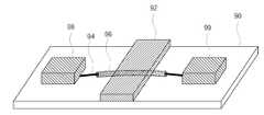
도시한 바와 같이, 기판(90) 상에 게이트 전극(92)을 형성하고, 상기 게이트 전극(92)의 양측에 소스 및 드레인 전극(98,99)을 형성한다.As shown, the
이때, 상기 소스 및 드레인 전극(98,99)을 형성하기 이전, 상기 게이트 전극(92)의 상부에 걸쳐 실리콘 나노와이어(94)를 구성하며, 상기 실리콘 나노 와이어(94)의 양측은 각각 상기 소스 및 드레인 전극(98,99)과 접촉하도록 구성된다.In this case, before forming the source and drain
그런데, 전술한 구성은 상기 나노 와이어(94)양단의 절연막(96)을 제거하고 상기 소스 및 드레인 전극(98,99)을 형성해야 한다.However, the above-described configuration should remove the insulating
이와 같이, 전기적 연결을 위한 공정이 추가되면서 공정 단계뿐만 아니라, 상기 나노 와이어가 상기 게이트 전극의 상부에서 불안정하게 위치하기 때문에, 금속과 반도체층의 전기적 접촉 상태가 불안정하여 소자의 동작특성에 많은 변이를 야기하게 된다.As such, as the process for electrical connection is added, not only the process step but also the nanowire is unstable at the top of the gate electrode, the electrical contact state between the metal and the semiconductor layer is unstable, resulting in many variations in operating characteristics of the device. Will cause.
본 발명은 전술한 문제를 해결하기 위해 제안된 것으로, 실리콘 나노 와이어를 포함하는 박막트랜지스터를 구성함에 있어, 더욱 안정화된 동작특성을 보이는 나노 와이어 박막트랜지스터를 형성하는 것을 목적으로 한다.The present invention has been proposed to solve the above-described problem, and in constructing a thin film transistor including silicon nanowires, an object of the present invention is to form a nanowire thin film transistor having more stable operation characteristics.
전술한 목적을 달성하기 위한 본 발명에 따른 나노 와이어 박막트랜지스터는 나노 와이어를 보강하는 구조를 도입함과 동시에, 외부 공정 변수와는 독립적인 소자로 구성하는 것이 가능하도록 한다.Nanowire thin film transistor according to the present invention for achieving the above object is to be introduced into the structure to reinforce the nanowire, and to be configured as a device independent of external process parameters.
이와 같이 하면, 안정한 동작특성을 보이는 스위칭 소자를 형성할 수 있는 동시에, 단순한 공정으로 스위칭 소자를 형성할 수 있는 장점이 있다.In this way, it is possible to form a switching element exhibiting stable operation characteristics, and there is an advantage in that the switching element can be formed by a simple process.
전술한 바와 같은 목적을 달성하기 위한 본 발명의 제 1 특징에 따른 나노 와이어 박막트랜지스터는 기판과; 기판 상에 구성된 실리콘 나노와이어(nano-wire)와; 상기 실리콘 나노 와이어를 고정하며, 상기 실리콘 나노 와이어의 양측을 노출하는 고정부와; 상기 노출된 양측의 상기 실리콘 나노 와이어와 접촉하는 소스 전극과 드레인 전극과, 상기 소스 및 드레인 전극의 이격된 중심에 위치하는 게이트 전극을 포함한다.According to a first aspect of the present invention, there is provided a thin film transistor comprising: a substrate; Silicon nanowires formed on the substrate; A fixing part fixing the silicon nanowires and exposing both sides of the silicon nanowires; A source electrode and a drain electrode contacting the exposed silicon nanowires; and a gate electrode positioned at a spaced center of the source and drain electrodes.
상기 나노 와이어는, 실리콘 결정이 일축성 방향으로 성장한 막대 형상인 것을 특징으로 한다.The nanowires are characterized by having a rod shape in which silicon crystals grow in a uniaxial direction.
본 발명의 제 1 특징에 따른 액정표시장치용 어레이기판은 기판과; 기판 상에 구성된 실리콘 나노 와이어(nano-wire)와; 상기 실리콘 나노 와이어를 고정하며, 상기 실리콘 나노 와이어의 양측을 노출하는 고정부와; 상기 노출된 양측의 상기 실리콘 나노 와이어와 접촉하는 소스 전극과 드레인 전극과, 상기 제 1 소스 및 드레인 전극의 이격된 중심에 위치하는 게이트 전극과; 상기 제 1 소스 및 드레인 전극과 접촉하여 구성된 제 2 소스 전극과 제 2 드레인 전극과; 상기 제 2 드레인 전극과 접촉하는 화소 전극을 포함한다.An array substrate for a liquid crystal display device according to a first aspect of the present invention includes a substrate; Silicon nanowires formed on the substrate; A fixing part fixing the silicon nanowires and exposing both sides of the silicon nanowires; A source electrode and a drain electrode in contact with the exposed silicon nanowires, and a gate electrode positioned at a spaced center of the first source and drain electrode; A second source electrode and a second drain electrode configured to contact the first source and drain electrodes; And a pixel electrode in contact with the second drain electrode.
상기 나노 와이어는, 실리콘 결정이 일축성 방향으로 성장한 막대 형상인 것을 특징하며, 상기 제 1 소스 및 드레인 전극과 제 2 소스 및 드레인 전극 사이에 게이트 절연막이 구성되고, 상기 화소 전극과 상기 제 2 드레인 전극 사이에 보호막이 구성된다.The nanowire has a rod shape in which silicon crystals grow in a uniaxial direction, and a gate insulating film is formed between the first source and drain electrodes and the second source and drain electrodes, and the pixel electrode and the second drain. A protective film is formed between the electrodes.
본 발명의 제 1 특징에 따른 나노 와이어 박막트랜지스터 제조방법은 기판을 준비하는 단계와; 상기 기판 상에 실리콘 나노 와이어(nano-wire)를 구성하는 단계와; 상기 실리콘 나노 와이어를 고정하며, 상기 실리콘 나노 와이어의 양측을 노출하는 고정부를 형성하는 단계와; 상기 노출된 양측의 상기 실리콘 나노 와이어와 접촉하는 소스 전극과 드레인 전극과, 상기 소스 및 드레인 전극의 이격된 중심에 위치하는 게이트 전극을 형성하는 단계를 포함한다.Nanowire thin film transistor manufacturing method according to a first aspect of the present invention comprises the steps of preparing a substrate; Constructing silicon nanowires on the substrate; Fixing the silicon nanowires to form fixing parts exposing both sides of the silicon nanowires; Forming a source electrode and a drain electrode in contact with the exposed silicon nanowires; and a gate electrode positioned at a spaced center of the source and drain electrodes.
상기 실리콘 나노 와이어는, 계면활성제를 포함하는 용매에 분산한 실리콘 나노 와이어를 스핀코팅방식으로 도포한 후, 히팅에 의해 용매를 제거하여 구성하는 것을 특징으로 한다.The silicon nanowires are formed by spin coating a silicon nanowire dispersed in a solvent containing a surfactant, and then removing the solvent by heating.
본 발명의 제 1 특징에 따른 액정표시장치용 어레이기판 제조방법은 기판을 준비하는 단계와; 상기 기판 상에 실리콘 나노 와이어(nano-wire)를 산포하는 단계와; 상기 실리콘 나노 와이어를 고정하며, 상기 실리콘 나노 와이어의 양측을 노출하는 고정부를 형성하는 단계와; 상기 노출된 양측의 상기 실리콘 나노 와이어와 접촉하는 소스 전극과 드레인 전극과, 상기 제 1 소스 및 드레인 전극의 이격된 중심에 위치하는 게이트 전극을 형성하는 단계와; 상기 제 1 소스 및 드레인 전극과 접촉하여 구성된 제 2 소스 전극과 제 2 드레인 전극을 형성하는 단계와; 상기 제 2 드레인 전극과 접촉하는 화소 전극을 형성하는 단계을 포함한다.An array substrate manufacturing method for a liquid crystal display device according to a first aspect of the present invention includes the steps of preparing a substrate; Dispersing silicon nanowires on the substrate; Fixing the silicon nanowires to form fixing parts exposing both sides of the silicon nanowires; Forming a source electrode and a drain electrode in contact with the exposed silicon nanowires, and a gate electrode positioned at a spaced center of the first source and drain electrode; Forming a second source electrode and a second drain electrode configured to contact the first source and drain electrodes; Forming a pixel electrode in contact with the second drain electrode.
본 발명의 제 2 특징에 따른 나노 와이어 박막트랜지스터 제조방법은 기판을 준비하는 단계와; 상기 기판 상에 실리콘 나노 와이어(nano-wire)를 구성하는 단계와; 상기 실리콘 나노 와이어를 고정하며, 상기 실리콘 나노 와이어의 양측을 노출하는 고정부와 게이트 절연막과 게이트 전극을 순차 형성하는 단계와; 상기 노출된 양측의 상기 실리콘 나노 와이어와 접촉하는 소스 전극과 드레인 전극을 형성하는 단계를 포함한다.A nanowire thin film transistor manufacturing method according to a second aspect of the present invention comprises the steps of preparing a substrate; Constructing silicon nanowires on the substrate; Fixing the silicon nanowires and sequentially forming a fixing portion, a gate insulating layer, and a gate electrode exposing both sides of the silicon nanowires; Forming a source electrode and a drain electrode in contact with the exposed silicon nanowires.
본 발명의 제 2 특징에 따른 액정표시장치용 어레이기파나 제조방법은 기판을 준비하는 단계와; 상기 기판 상에 실리콘 나노 와이어(nano-wire)를 산포하는 단계와; 상기 실리콘 나노 와이어를 고정하며, 상기 실리콘 나노 와이어의 양측을 노출하는 고정부를 형성하는 단계와; 상기 노출된 양측의 상기 실리콘 나노 와이어와 접촉하는 소스 전극과 드레인 전극과, 상기 제 1 소스 및 드레인 전극의 이격된 중심에 위치하는 게이트 전극을 형성하는 단계와; 상기 제 1 소스 및 드레인 전극과 접촉하여 구성된 제 2 소스 전극과 제 2 드레인 전극을 형성하는 단계와; 상기 제 2 드레인 전극과 접촉하는 화소 전극을 형성하는 단계을 포함한다.According to a second aspect of the present invention, there is provided an array wave or manufacturing method for a liquid crystal display device comprising the steps of: preparing a substrate; Dispersing silicon nanowires on the substrate; Fixing the silicon nanowires to form fixing parts exposing both sides of the silicon nanowires; Forming a source electrode and a drain electrode in contact with the exposed silicon nanowires, and a gate electrode positioned at a spaced center of the first source and drain electrode; Forming a second source electrode and a second drain electrode configured to contact the first source and drain electrodes; Forming a pixel electrode in contact with the second drain electrode.
이하, 도면을 참조하여 본 발명에 따른 바람직한 실시예를 설명한다.Hereinafter, with reference to the drawings will be described a preferred embodiment according to the present invention.
-- 제 1 실시예 --First Embodiment
본 발명은 액티브층으로 실리콘 나노 와이어(Si nano-wire)사용하고, 소스 및 드레인 전극과 게이트 전극을 동일한 도전성 금속물질로 형성하는 것을 특징으로 한다.The present invention is characterized in that a silicon nanowire (Si nano-wire) is used as an active layer, and the source and drain electrodes and the gate electrode are formed of the same conductive metal material.
이하, 도 6을 참조하여 본 발명에 따른 나노 와이어 박막트랜지스터를 형성하는 공정을 설명한다.Hereinafter, a process of forming a nanowire thin film transistor according to the present invention will be described with reference to FIG. 6.
도 6a 내지 도 6c 본 발명의 제 1 실시예에 따른 나노 와이어 박막트랜지스터의 제조공정을 공정순서에 따라 도시한 공정 단면도이다.6A to 6C are cross-sectional views illustrating a manufacturing process of a nanowire thin film transistor according to a first embodiment of the present invention according to a process sequence.
도 6a에 도시한 바와 같이, 기판(100) 상에 실리콘 나노 와이어(silicon nano-wire)(102)를 구성한다.As shown in FIG. 6A, silicon nano-
상기 실리콘 나노 와이어(102)는 반도체 기판(미도시) 상에 나노(nano)크기를 가지는 촉매를 증착하고, 상기 촉매가 증착된 반도체 기판 상에서 실리콘과 반응성 가스를 이용하여 일축성(coaxial) 방향으로 결정 성장시키는 공정을 진행하여 형성한다.The
이러한 나노 와이어(nano-wire)는 별도의 제품으로 제작된 것을 소정의 방법으로 기판(100)상에 산포하여 구성하는 방법을 사용할 수 있다.Such nano-wires may be formed by dispersing and forming a separate product on the
상기 나노 와이어(102)는 일축성 방향으로 성장한 실리콘결정의 표면에 절연막이 형성된 상태이다.The
다음으로, 상기 나노 와이어(nano-wire)를 구성한 기판(100)의 전면에 벤조사이클로부텐(BCB)과 아크릴(acryl)계 수지를 포함하는 유기 절연물질을 도포하여 상기 나노 와이어(102)를 고정하는 고정부(104)를 형성한다.Next, the
도 6b에 도시한 바와 같이, 상기 고정부(104)를 제거하여, 상기 나노 와이어(102)의 양측을 노출하는 제 1 콘택홀(106)과 제 2 콘택홀(108)을 형성한다.As shown in FIG. 6B, the fixing
이때, 상기 제 1 및 제 2 콘택홀(106,108)을 형성하는 공정 중, 상기 나노 와이어(102) 표면의 산화막이 제거되도록 할 수 있으며 만약, 이러한 공정이 가능하지 않은 경우는 별도로 제거해주면 된다.In this case, during the process of forming the first and second contact holes 106 and 108, the oxide film on the surface of the
도 6c에 도시한 바와 같이, 상기 고정부(104)가 형성된 기판(100)의 전면에 알루미늄(Al), 알루미늄합금(AlNd),구리(Cu), 텅스텐(W), 몰리브덴(Mo),티타늄(Ti),크롬(Cr)등을 포함하는 도전성 금속 그룹 중 선택된 하나를 증착하여, 상기 제 1 및 제 2 콘택홀(106,108)을 통해 하부의 나노 와이어(nano wire)와 접촉하는 소스 전극(110)과 드레인 전극(112)과, 상기 소스 및 드레인 전극(110,112)의 이격된 공간에 게이트 전극(114)을 형성한다.As shown in FIG. 6C, aluminum (Al), aluminum alloy (AlNd), copper (Cu), tungsten (W), molybdenum (Mo), and titanium are disposed on the entire surface of the
이때, 상기 소스 및 드레인 전극(110,112)과 실리콘 나노 와이어(102)의 계면에서 형성된 실리사이드(silicide)상기 소스 및 드레인 전극(110,112)과 나노 와이어(nano-wire)의 오믹 콘택(ohmic contact)역활을 하기 때문에 별도로 오믹 콘택층을 형성하는 공정이 필요치 않다.At this time, the silicide formed at the interface between the source and drain
이와 같은 공정으로 나노 와이어 박막트랜지스터를 제작할 수 있으며, 이를 스위칭 소자로 사용한 액정표시장치용 어레이 기판의 제작공정을 이하, 도 6d 내지 도 6e를 참조하여 설명한다.A nanowire thin film transistor can be manufactured by such a process, and a manufacturing process of an array substrate for a liquid crystal display device using the same as a switching element will be described below with reference to FIGS. 6D to 6E.
도 6d에 도시한 바와 같이, 상기 소스 및 드레인 전극(110,112)과 게이트 전 극(114)이 형성된 기판(100)의 전면에 질화 실리콘(SiNX)과 산화 실리콘(SiO2)을 포함하는 무기절연물질 그룹 중 선택된 하나를 증착하여 게이트 절연막(116)을 형성하고 이를 패턴하여 제 1 및 제 2 콘택홀(118,120)을 형성한다.As shown in FIG. 6D, an inorganic insulation including silicon nitride (SiNX ) and silicon oxide (SiO2 ) is formed on the entire surface of the
다음으로, 상기 제 1 및 제 2 콘택홀(118,120)이 형성된 게이트 절연막(116)의 전면에 앞서 언급한 도전성 금속을 증착하고 패턴하여, 상기 소스 전극(110)과 접촉하는 제 2 소스 전극 및 데이터 배선(122, 미도시)을 형성하고, 상기 드레인 전극(112)과 접촉하는 제 2 드레인 전극(124)을 형성한다.Next, a second source electrode and data contacting the
도 6e에 도시한 바와 같이, 상기 제 2 소스 및 드레인 전극(122,124)이 형성된 기판(100)의 전면에 질화 실리콘(SiNX)과 산화 실리콘(SiO2)을 포함하는 무기절연물질 그룹 중 선택된 하나 또는 그 이상의 물질을 증착하거나, 경우에 따라서 벤조사이클로부텐(BCB)과 아크릴(acryl)계 수지(resin)를 포함하는 유기절연물질 그룹 중 선택된 하나 또는 그 이상의 물질을 증착하여 보호막(126)을 형성한다.As shown in FIG. 6E, one selected from the group of inorganic insulating materials including silicon nitride (SiNX ) and silicon oxide (SiO2 ) on the entire surface of the
다음으로, 상기 보호막(126)을 패턴하여 상기 제 2 드레인 전극(124)의 일부를 노출하는 드레인 콘택홀(128)을 형성한다.Next, the
상기 보호막(126)이 형성된 기판(100)의 전면에 인듐-틴-옥사이드(ITO)와 인듐-징크-옥사이드(IZO)를 포함하는 투명한 도전성 금속 그룹 중 선택된 하나를 증차하고 패턴하여, 상기 제 2 드레인 전극(124)과 접촉하는 화소 전극(130)을 형성한다.The second layer is formed by increasing and patterning a selected one of a transparent conductive metal group including indium tin oxide (ITO) and indium zinc oxide (IZO) on the entire surface of the
전술한 공정을 통해, 상기 나노 와이어 박막트랜지스터를 스위칭 소자로 사 용하는 액정표시장치용 어레이 기판을 제작할 수 있다.Through the above-described process, an array substrate for a liquid crystal display device using the nanowire thin film transistor as a switching element can be manufactured.
이하, 본 발명의 제 2 실시예를 통해 앞서 설명한 나노 와이어 박막트랜지스터의 변형예를 설명한다.Hereinafter, a modified example of the nanowire thin film transistor described above will be described through a second embodiment of the present invention.
-- 제 2 실시예 --Second Embodiment
본 발명에 따른 제 2 실시예는 실리콘 나노 와이어를 스핀코팅 방식으로 기판에 구성하는 것을 특징으로 한다.A second embodiment according to the present invention is characterized in that the silicon nanowires are formed on the substrate by spin coating.
도 7a 내지 도 7e는 본 발명의 제 2 실시예에 따른 나노 와이어 박막트랜지스터의 제조공정을 공정순서에 따라 도시한 공정 단면도이다.7A to 7E are cross-sectional views illustrating a manufacturing process of a nanowire thin film transistor according to a second embodiment of the present invention according to a process sequence.
도 7a에 도시한 바와 같이, 기판(200) 상에 실리콘 나노 와이어(silicon nano-wire)(202)를 구성한다.As shown in FIG. 7A, a silicon nano-
상기 실리콘 나노 와이어(202)를 계면활성제를 포함하는 용매에 분산시키고, 상기 나노 와이어를 포함하는 용매를 스핀코팅방식으로 기판(200)에 분산시켜 구성하는 방법을 사용한다.The
상기 실리콘 나노 와이어(202)는 앞서 언급한바와 같이, 반도체 기판(미도시) 상에 나노(nano)크기를 가지는 촉매를 증착하고, 상기 촉매가 증착된 반도체 기판(200) 상에서 실리콘(Si)과 반응성 가스를 이용하여 일축성(coaxial)방향으로 결정 성장시키는 공정을 진행하여 형성한다.As described above, the
상기 나노 와이어(202)는 일축성 방향으로 성장한 실리콘결정의 표면에 절연막이 형성된 상태이다.The
다음으로 도 7b에 도시한 바와 같이, 상기 나노 와이어(202)가 형성된 기판(200)을 100℃이하의 온도로 히팅(heating)함으로써, 상기 나노 와이어(202)에 잔류한 용매를 제거하는 공정을 진행한다.Next, as shown in FIG. 7B, a process of removing the solvent remaining in the
도 7c에 도시한 바와 같이, 상기 나노 와이어(nano-wire)의 중심에 고정부(204)와 게이트 절연막(206)과 게이트 전극(208)을 적층하여 형성한다.As shown in FIG. 7C, the fixing
전술한 구성에서, 상기 고정부(204)와 상기 게이트 절연막(206)은 순차 증착되고 동시에 패턴되어 형성할 수 있다.In the above-described configuration, the fixing
이때, 상기 고정부(204)와 게이트 절연막(206)을 패턴하는 공정에서 상기 노출된 나노 와이어 표면을 감싸는 산화막(미도시)을 제거할 수 있다.In this case, in the process of patterning the fixing
또는, 상기 게이트 전극(208)을 형성한 후, 게이트 전극(208)을 식각방지막으로 하여 상기 나노 와이어(202) 표면의 산화막(미도시)을 제거할 수 도 있다.Alternatively, after the
도 7d에 도시한 바와 같이, 상기 게이트 전극(208)이 형성된 기판(200)의 전면에 알루미늄(Al), 알루미늄합금(AlNd),구리(Cu), 텅스텐(W), 몰리브덴(Mo),티타늄(Ti),크롬(Cr)등을 포함하는 도전성 금속그룹 중 선택된 하나를 증착하고 패턴하여 상기 게이트 전극을 중심으로 양측에 각각 위치하여 노출된 나노 와이어(202)와 접촉하는 소스 전극과 드레인 전극(210,212)을 형성한다.As shown in FIG. 7D, aluminum (Al), aluminum alloy (AlNd), copper (Cu), tungsten (W), molybdenum (Mo), and titanium are formed on the entire surface of the
전술한 공정에서, 상기 소스 및 드레인 전극(210,212)과 실리콘 나노 와이어(202)의 계면에서 형성된 실리사이드(silicide)상기 소스 및 드레인 전극(110,112)과 나노 와이어(nano-wire)의 오믹 콘택(ohmic contact)역활을 하기 때문에 별도로 오믹 콘택층을 형성하는 공정이 필요치 않다.In the above process, silicide formed at an interface between the source and drain
전술한 공정을 통해 본 발명의 제 2 실시예에 따른 나노 와이어 박막트랜지스터를 형성할 수 있다.Through the above-described process, it is possible to form the nanowire thin film transistor according to the second embodiment of the present invention.
이하, 도 7e 내지 도 7f를 참조하여 상기 나노 와이어 박막트랜지스터를 포함하는 액정표시장치용 어레이 기판의 형성공정을 도시한 도면이다.Hereinafter, a process of forming an array substrate for a liquid crystal display device including the nanowire thin film transistor will be described with reference to FIGS. 7E to 7F.
도 7e에 도시한 바와 같이, 상기 소스 및 드레인 전극(210,212)이 형성된 기판(200)의 전면에 질화 실리콘(SiNX)과 산화 실리콘(SiO2)을 포함하는 무기절연물질 그룹 중 선택된 하나를 증착하여 제 1 절연막(214)을 형성하고 이를 패턴하여 상기 소스 전극(210)과 드레인 전극(212)을 노출하는 제 1 콘택홀(216)과 제 2 콘택홀(218)을 형성한다.As shown in FIG. 7E, one selected from the group of inorganic insulating materials including silicon nitride (SiNX ) and silicon oxide (SiO2 ) is deposited on the entire surface of the
다음으로, 상기 제 1 및 제 2 콘택홀(216,218)이 형성된 제 1 절연막(214)의 전면에 앞서 언급한 도전성 금속을 증착하고 패턴하여, 상기 소스 전극(210)과 접촉하는 제 2 소스 전극 및 데이터 배선(220, 미도시)을 형성하고, 상기 드레인 전극(212)과 접촉하는 제 2 드레인 전극(222)을 형성한다.Next, a second source electrode contacting the
도 7f에 도시한 바와 같이, 상기 제 2 소스 및 드레인 전극(220,222)이 형성된 기판(200)의 전면에 질화 실리콘(SiNX)과 산화 실리콘(SiO2)을 포함하는 무기절연물질 그룹 중 선택된 하나 또는 그 이상의 물질을 증착하거나, 경우에 따라서 벤조사이클로부텐(BCB)과 아크릴(acryl)계 수지(resin)를 포함하는 유기절연물질 그룹 중 선택된 하나 또는 그 이상의 물질을 증착하여 제 2 절연막인 보호막(224)을 형성한다.As shown in FIG. 7F, one selected from the group of inorganic insulating materials including silicon nitride (SiNX ) and silicon oxide (SiO2 ) on the entire surface of the
다음으로, 상기 보호막(224)을 패턴하여 상기 제 2 드레인 전극(222)의 일부를 노출하는 드레인 콘택홀(226)을 형성한다.Next, the
상기 보호막(224)이 형성된 기판(200)의 전면에 인듐-틴-옥사이드(ITO)와 인듐-징크-옥사이드(IZO)를 포함하는 투명한 도전성 금속 그룹 중 선택된 하나를 증차하고 패턴하여, 상기 제 2 드레인 전극(222)과 접촉하는 화소 전극(228)을 형성한다.The second layer is formed by increasing and patterning one selected from a group of transparent conductive metals including indium tin oxide (ITO) and indium zinc oxide (IZO) on the entire surface of the
전술한 공정을 통해 본 발명의 제 2 실시예에 따른 나노 와이어 박막트랜지스터를 제작할 수 있다.Through the above-described process, it is possible to manufacture a nano-wire thin film transistor according to the second embodiment of the present invention.
본 발명에 따른 나노 와이어 박막트랜지스터는 나노 와이어를 고정하고 보강하는 구조를 도입함으로써 박막트랜지스터의 동작 특성이 안정화되는 효과가 있다.The nanowire thin film transistor according to the present invention has an effect of stabilizing the operating characteristics of the thin film transistor by introducing a structure for fixing and reinforcing nanowires.
또한, 액티브층을 실리콘 나노 와이어로 구성함으로써, 상기 박막트랜지스터의 각 전극과 접촉하는 게이트 배선과 데이터 배선과는 별도로 상기 박막트랜지스터 소자를 독립적으로 구성할 수 있기 때문에, 상기 게이트 및 데이터 배선에 따라 물질을 달리 할 필요 없이 상기 소스 및 드레인 전극과 게이트 전극을 동일한 물질로 형성하는 것이 가능하여 공정을 단순화 할 수 있고 이에 따른 공정시간 단축 및 공정 비용을 절감할 수 있는 효과가 있다.In addition, since the active layer is formed of silicon nanowires, the thin film transistor element can be independently configured from the gate line and the data line in contact with each electrode of the thin film transistor. It is possible to form the source and drain electrodes and the gate electrode with the same material without the need to change the process to simplify the process, thereby reducing the process time and the process cost can be reduced.
Claims (25)
Translated fromKoreanPriority Applications (6)
| Application Number | Priority Date | Filing Date | Title |
|---|---|---|---|
| KR1020050029120AKR101145146B1 (en) | 2005-04-07 | 2005-04-07 | TFT and method of fabricating of the same |
| US11/397,556US7704806B2 (en) | 2005-04-07 | 2006-04-05 | Thin film transistor having silicon nanowire and method of fabricating the same |
| CNB2006100731407ACN100472813C (en) | 2005-04-07 | 2006-04-06 | Thin film transistor and manufacturing method thereof |
| JP2006106321AJP4580890B2 (en) | 2005-04-07 | 2006-04-07 | Thin film transistor, array substrate for flat panel display, method for manufacturing thin film transistor, and method for manufacturing array substrate for flat panel display |
| US12/721,124US8426869B2 (en) | 2005-04-07 | 2010-03-10 | Thin film transistor and method of fabricating the same |
| US13/849,906US8610128B2 (en) | 2005-04-07 | 2013-03-25 | Thin film transistor method of fabricating the same |
Applications Claiming Priority (1)
| Application Number | Priority Date | Filing Date | Title |
|---|---|---|---|
| KR1020050029120AKR101145146B1 (en) | 2005-04-07 | 2005-04-07 | TFT and method of fabricating of the same |
Publications (2)
| Publication Number | Publication Date |
|---|---|
| KR20060107107A KR20060107107A (en) | 2006-10-13 |
| KR101145146B1true KR101145146B1 (en) | 2012-05-14 |
Family
ID=37064267
Family Applications (1)
| Application Number | Title | Priority Date | Filing Date |
|---|---|---|---|
| KR1020050029120AExpired - Fee RelatedKR101145146B1 (en) | 2005-04-07 | 2005-04-07 | TFT and method of fabricating of the same |
Country Status (4)
| Country | Link |
|---|---|
| US (3) | US7704806B2 (en) |
| JP (1) | JP4580890B2 (en) |
| KR (1) | KR101145146B1 (en) |
| CN (1) | CN100472813C (en) |
Cited By (1)
| Publication number | Priority date | Publication date | Assignee | Title |
|---|---|---|---|---|
| KR20160042741A (en) | 2014-10-10 | 2016-04-20 | 전북대학교산학협력단 | Bag Combined with Chair |
Families Citing this family (48)
| Publication number | Priority date | Publication date | Assignee | Title |
|---|---|---|---|---|
| US8029186B2 (en)* | 2004-11-05 | 2011-10-04 | International Business Machines Corporation | Method for thermal characterization under non-uniform heat load |
| US7426000B2 (en)* | 2005-04-14 | 2008-09-16 | Samsung Electronics Co., Ltd. | Transistor, display device including the same, and manufacturing method thereof |
| KR101287735B1 (en)* | 2006-12-08 | 2013-07-18 | 엘지디스플레이 주식회사 | Method of manufacturing thin film transistor and method of manufacturing liquid crystal display device using the same |
| KR101318083B1 (en)* | 2006-12-29 | 2013-10-14 | 엘지디스플레이 주식회사 | Array substrate manufacturing method |
| US7948050B2 (en)* | 2007-01-11 | 2011-05-24 | International Business Machines Corporation | Core-shell nanowire transistor |
| KR101311301B1 (en)* | 2007-02-09 | 2013-09-25 | 엘지디스플레이 주식회사 | Nanowire transistor and manufacturing method thereof |
| KR100972842B1 (en) | 2007-09-11 | 2010-07-28 | 포항공과대학교 산학협력단 | Nanodevices containing nanorods and methods of manufacturing the same |
| EP2197782B1 (en) | 2007-09-12 | 2020-03-04 | Smoltek AB | Connecting and bonding adjacent layers with nanostructures |
| JP2011501361A (en)* | 2007-10-15 | 2011-01-06 | イー・アイ・デュポン・ドウ・ヌムール・アンド・カンパニー | Backplane structure for solution-processed electronic devices |
| KR20100105673A (en) | 2007-12-14 | 2010-09-29 | 이 아이 듀폰 디 네모아 앤드 캄파니 | Backplane structures for electronic devices |
| KR101424816B1 (en)* | 2008-02-18 | 2014-07-31 | 삼성전자주식회사 | Thin film transistor including nanowire and method of manufacturing the same |
| RU2010138584A (en) | 2008-02-25 | 2012-04-10 | Смольтек Аб (Se) | DEPOSITION AND SELECTIVE REMOVAL OF ELECTRICAL WIRING AUXILIARY LAYER FOR PROCESSING NANOSTRUCTURE |
| US9343490B2 (en) | 2013-08-09 | 2016-05-17 | Zena Technologies, Inc. | Nanowire structured color filter arrays and fabrication method of the same |
| US8889455B2 (en)* | 2009-12-08 | 2014-11-18 | Zena Technologies, Inc. | Manufacturing nanowire photo-detector grown on a back-side illuminated image sensor |
| US8519379B2 (en) | 2009-12-08 | 2013-08-27 | Zena Technologies, Inc. | Nanowire structured photodiode with a surrounding epitaxially grown P or N layer |
| US20110115041A1 (en)* | 2009-11-19 | 2011-05-19 | Zena Technologies, Inc. | Nanowire core-shell light pipes |
| US8507840B2 (en) | 2010-12-21 | 2013-08-13 | Zena Technologies, Inc. | Vertically structured passive pixel arrays and methods for fabricating the same |
| US9299866B2 (en) | 2010-12-30 | 2016-03-29 | Zena Technologies, Inc. | Nanowire array based solar energy harvesting device |
| US8748799B2 (en) | 2010-12-14 | 2014-06-10 | Zena Technologies, Inc. | Full color single pixel including doublet or quadruplet si nanowires for image sensors |
| US8384007B2 (en)* | 2009-10-07 | 2013-02-26 | Zena Technologies, Inc. | Nano wire based passive pixel image sensor |
| US8269985B2 (en) | 2009-05-26 | 2012-09-18 | Zena Technologies, Inc. | Determination of optimal diameters for nanowires |
| US9478685B2 (en) | 2014-06-23 | 2016-10-25 | Zena Technologies, Inc. | Vertical pillar structured infrared detector and fabrication method for the same |
| US8546742B2 (en)* | 2009-06-04 | 2013-10-01 | Zena Technologies, Inc. | Array of nanowires in a single cavity with anti-reflective coating on substrate |
| US9515218B2 (en)* | 2008-09-04 | 2016-12-06 | Zena Technologies, Inc. | Vertical pillar structured photovoltaic devices with mirrors and optical claddings |
| US8835831B2 (en) | 2010-06-22 | 2014-09-16 | Zena Technologies, Inc. | Polarized light detecting device and fabrication methods of the same |
| US20100304061A1 (en)* | 2009-05-26 | 2010-12-02 | Zena Technologies, Inc. | Fabrication of high aspect ratio features in a glass layer by etching |
| US8299472B2 (en)* | 2009-12-08 | 2012-10-30 | Young-June Yu | Active pixel sensor with nanowire structured photodetectors |
| US8735797B2 (en) | 2009-12-08 | 2014-05-27 | Zena Technologies, Inc. | Nanowire photo-detector grown on a back-side illuminated image sensor |
| US8791470B2 (en) | 2009-10-05 | 2014-07-29 | Zena Technologies, Inc. | Nano structured LEDs |
| US8274039B2 (en) | 2008-11-13 | 2012-09-25 | Zena Technologies, Inc. | Vertical waveguides with various functionality on integrated circuits |
| US8866065B2 (en) | 2010-12-13 | 2014-10-21 | Zena Technologies, Inc. | Nanowire arrays comprising fluorescent nanowires |
| US8229255B2 (en)* | 2008-09-04 | 2012-07-24 | Zena Technologies, Inc. | Optical waveguides in image sensors |
| US8890271B2 (en) | 2010-06-30 | 2014-11-18 | Zena Technologies, Inc. | Silicon nitride light pipes for image sensors |
| US9406709B2 (en) | 2010-06-22 | 2016-08-02 | President And Fellows Of Harvard College | Methods for fabricating and using nanowires |
| US9000353B2 (en) | 2010-06-22 | 2015-04-07 | President And Fellows Of Harvard College | Light absorption and filtering properties of vertically oriented semiconductor nano wires |
| US9082673B2 (en) | 2009-10-05 | 2015-07-14 | Zena Technologies, Inc. | Passivated upstanding nanostructures and methods of making the same |
| US20100148221A1 (en)* | 2008-11-13 | 2010-06-17 | Zena Technologies, Inc. | Vertical photogate (vpg) pixel structure with nanowires |
| KR20100073247A (en)* | 2008-12-23 | 2010-07-01 | 한국전자통신연구원 | Self aligned field effect transistor structure |
| US9368599B2 (en)* | 2010-06-22 | 2016-06-14 | International Business Machines Corporation | Graphene/nanostructure FET with self-aligned contact and gate |
| US8900935B2 (en) | 2011-01-25 | 2014-12-02 | International Business Machines Corporation | Deposition on a nanowire using atomic layer deposition |
| KR101425064B1 (en) | 2011-06-09 | 2014-08-01 | 엘지디스플레이 주식회사 | Oxide thin film transistor and method of fabricating the same |
| US20140044865A1 (en)* | 2012-01-31 | 2014-02-13 | Hossam Haick | Method for manufacturing a nano-wire array and a device that comprises a nano-wire array |
| CN103022150B (en) | 2012-12-25 | 2015-05-20 | 京东方科技集团股份有限公司 | Thin film transistor, method for manufacturing same, array substrate and display device |
| CN103943509B (en)* | 2014-04-11 | 2017-02-15 | 深圳市华星光电技术有限公司 | Manufacture procedure method of thin film transistor |
| US10217819B2 (en)* | 2015-05-20 | 2019-02-26 | Samsung Electronics Co., Ltd. | Semiconductor device including metal-2 dimensional material-semiconductor contact |
| CN107768386B (en)* | 2017-11-16 | 2020-09-01 | 深圳市华星光电半导体显示技术有限公司 | TFT array substrate and its manufacturing method and liquid crystal display panel |
| CN111916338B (en)* | 2019-05-08 | 2023-07-25 | 京东方科技集团股份有限公司 | A silicon-based nanowire, its preparation method and thin film transistor |
| CN112018032A (en) | 2019-05-13 | 2020-12-01 | 京东方科技集团股份有限公司 | An array substrate, its preparation method and display panel |
Citations (4)
| Publication number | Priority date | Publication date | Assignee | Title |
|---|---|---|---|---|
| JP2003347314A (en)* | 2002-04-16 | 2003-12-05 | Lg Phillips Lcd Co Ltd | Manufacturing method of array substrate for liquid crystal display |
| WO2004032190A2 (en)* | 2002-09-30 | 2004-04-15 | Nanosys, Inc. | Integrated displays using nanowire transistors |
| US20040112964A1 (en)* | 2002-09-30 | 2004-06-17 | Nanosys, Inc. | Applications of nano-enabled large area macroelectronic substrates incorporating nanowires and nanowire composites |
| US20040136866A1 (en)* | 2002-06-27 | 2004-07-15 | Nanosys, Inc. | Planar nanowire based sensor elements, devices, systems and methods for using and making same |
Family Cites Families (10)
| Publication number | Priority date | Publication date | Assignee | Title |
|---|---|---|---|---|
| TW511298B (en) | 1999-12-15 | 2002-11-21 | Semiconductor Energy Lab | EL display device |
| KR100848099B1 (en)* | 2002-05-27 | 2008-07-24 | 삼성전자주식회사 | Thin film transistor substrate for liquid crystal display |
| KR100441433B1 (en)* | 2001-04-12 | 2004-07-22 | 삼성에스디아이 주식회사 | flat panel display device and method for fabricating thereof |
| KR100380142B1 (en)* | 2001-07-18 | 2003-04-11 | 엘지.필립스 엘시디 주식회사 | Transflective liquid crystal display device |
| US6891227B2 (en)* | 2002-03-20 | 2005-05-10 | International Business Machines Corporation | Self-aligned nanotube field effect transistor and method of fabricating same |
| US7067867B2 (en)* | 2002-09-30 | 2006-06-27 | Nanosys, Inc. | Large-area nonenabled macroelectronic substrates and uses therefor |
| US7355216B2 (en)* | 2002-12-09 | 2008-04-08 | The Regents Of The University Of California | Fluidic nanotubes and devices |
| KR100669713B1 (en)* | 2004-03-26 | 2007-01-16 | 삼성에스디아이 주식회사 | Plasma display panel |
| CA2572798A1 (en)* | 2004-07-07 | 2006-07-27 | Nanosys, Inc. | Systems and methods for harvesting and integrating nanowires |
| KR100615233B1 (en)* | 2004-07-21 | 2006-08-25 | 삼성에스디아이 주식회사 | Thin film transistor, and flat panel display device having same |
- 2005
- 2005-04-07KRKR1020050029120Apatent/KR101145146B1/ennot_activeExpired - Fee Related
- 2006
- 2006-04-05USUS11/397,556patent/US7704806B2/ennot_activeExpired - Fee Related
- 2006-04-06CNCNB2006100731407Apatent/CN100472813C/ennot_activeExpired - Fee Related
- 2006-04-07JPJP2006106321Apatent/JP4580890B2/ennot_activeExpired - Fee Related
- 2010
- 2010-03-10USUS12/721,124patent/US8426869B2/enactiveActive
- 2013
- 2013-03-25USUS13/849,906patent/US8610128B2/enactiveActive
Patent Citations (4)
| Publication number | Priority date | Publication date | Assignee | Title |
|---|---|---|---|---|
| JP2003347314A (en)* | 2002-04-16 | 2003-12-05 | Lg Phillips Lcd Co Ltd | Manufacturing method of array substrate for liquid crystal display |
| US20040136866A1 (en)* | 2002-06-27 | 2004-07-15 | Nanosys, Inc. | Planar nanowire based sensor elements, devices, systems and methods for using and making same |
| WO2004032190A2 (en)* | 2002-09-30 | 2004-04-15 | Nanosys, Inc. | Integrated displays using nanowire transistors |
| US20040112964A1 (en)* | 2002-09-30 | 2004-06-17 | Nanosys, Inc. | Applications of nano-enabled large area macroelectronic substrates incorporating nanowires and nanowire composites |
Cited By (1)
| Publication number | Priority date | Publication date | Assignee | Title |
|---|---|---|---|---|
| KR20160042741A (en) | 2014-10-10 | 2016-04-20 | 전북대학교산학협력단 | Bag Combined with Chair |
Also Published As
| Publication number | Publication date |
|---|---|
| US8426869B2 (en) | 2013-04-23 |
| US20060226424A1 (en) | 2006-10-12 |
| CN100472813C (en) | 2009-03-25 |
| JP2006295176A (en) | 2006-10-26 |
| US20100163850A1 (en) | 2010-07-01 |
| US7704806B2 (en) | 2010-04-27 |
| US20130228750A1 (en) | 2013-09-05 |
| JP4580890B2 (en) | 2010-11-17 |
| KR20060107107A (en) | 2006-10-13 |
| CN1845341A (en) | 2006-10-11 |
| US8610128B2 (en) | 2013-12-17 |
Similar Documents
| Publication | Publication Date | Title |
|---|---|---|
| KR101145146B1 (en) | TFT and method of fabricating of the same | |
| JP4597901B2 (en) | Thin film transistor and manufacturing method thereof | |
| US8049830B2 (en) | Liquid crystal display device and fabrication method thereof | |
| US8735883B2 (en) | Oxide thin film transistor and method of fabricating the same | |
| CN103700665B (en) | Metal oxide thin-film transistor array base palte and preparation method thereof, display unit | |
| CN101814455A (en) | Method for manufacturing array substrate | |
| KR20080093709A (en) | Thin film transistor substrate and manufacturing method thereof | |
| JP5685565B2 (en) | Thin film transistor and manufacturing method thereof | |
| CN102053435A (en) | Liquid crystal display device and manufacturing method thereof | |
| KR101232170B1 (en) | Method For Fabricating Poly-Silicon Thin Film Transistors Array Substrate And Method For Fabricating Liquid Crystal Display Device By Applying Said | |
| JP4312179B2 (en) | Liquid crystal display element and manufacturing method thereof | |
| KR101136165B1 (en) | Thin Film Transistor and the fabrication method thereof | |
| KR100539583B1 (en) | Method for crystallizing Silicon and method for manufacturing Thin Film Transistor (TFT) using the same | |
| KR101018271B1 (en) | Method for manufacturing polycrystalline silicon thin film transistor | |
| KR20020024465A (en) | Array Panel used for a Liquid Crystal Display and method for fabricating the same |
Legal Events
| Date | Code | Title | Description |
|---|---|---|---|
| PA0109 | Patent application | St.27 status event code:A-0-1-A10-A12-nap-PA0109 | |
| PG1501 | Laying open of application | St.27 status event code:A-1-1-Q10-Q12-nap-PG1501 | |
| PN2301 | Change of applicant | St.27 status event code:A-3-3-R10-R13-asn-PN2301 St.27 status event code:A-3-3-R10-R11-asn-PN2301 | |
| T11-X000 | Administrative time limit extension requested | St.27 status event code:U-3-3-T10-T11-oth-X000 | |
| T12-X000 | Administrative time limit extension not granted | St.27 status event code:U-3-3-T10-T12-oth-X000 | |
| A201 | Request for examination | ||
| PA0201 | Request for examination | St.27 status event code:A-1-2-D10-D11-exm-PA0201 | |
| R18-X000 | Changes to party contact information recorded | St.27 status event code:A-3-3-R10-R18-oth-X000 | |
| D13-X000 | Search requested | St.27 status event code:A-1-2-D10-D13-srh-X000 | |
| D14-X000 | Search report completed | St.27 status event code:A-1-2-D10-D14-srh-X000 | |
| PE0902 | Notice of grounds for rejection | St.27 status event code:A-1-2-D10-D21-exm-PE0902 | |
| AMND | Amendment | ||
| E13-X000 | Pre-grant limitation requested | St.27 status event code:A-2-3-E10-E13-lim-X000 | |
| P11-X000 | Amendment of application requested | St.27 status event code:A-2-2-P10-P11-nap-X000 | |
| P13-X000 | Application amended | St.27 status event code:A-2-2-P10-P13-nap-X000 | |
| R18-X000 | Changes to party contact information recorded | St.27 status event code:A-3-3-R10-R18-oth-X000 | |
| R18-X000 | Changes to party contact information recorded | St.27 status event code:A-3-3-R10-R18-oth-X000 | |
| E601 | Decision to refuse application | ||
| PE0601 | Decision on rejection of patent | St.27 status event code:N-2-6-B10-B15-exm-PE0601 | |
| AMND | Amendment | ||
| E13-X000 | Pre-grant limitation requested | St.27 status event code:A-2-3-E10-E13-lim-X000 | |
| J201 | Request for trial against refusal decision | ||
| P11-X000 | Amendment of application requested | St.27 status event code:A-2-2-P10-P11-nap-X000 | |
| P13-X000 | Application amended | St.27 status event code:A-2-2-P10-P13-nap-X000 | |
| PJ0201 | Trial against decision of rejection | St.27 status event code:A-3-3-V10-V11-apl-PJ0201 | |
| PB0901 | Examination by re-examination before a trial | St.27 status event code:A-6-3-E10-E12-rex-PB0901 | |
| B701 | Decision to grant | ||
| PB0701 | Decision of registration after re-examination before a trial | St.27 status event code:A-3-4-F10-F13-rex-PB0701 | |
| GRNT | Written decision to grant | ||
| PR0701 | Registration of establishment | St.27 status event code:A-2-4-F10-F11-exm-PR0701 | |
| PR1002 | Payment of registration fee | St.27 status event code:A-2-2-U10-U11-oth-PR1002 Fee payment year number:1 | |
| PG1601 | Publication of registration | St.27 status event code:A-4-4-Q10-Q13-nap-PG1601 | |
| FPAY | Annual fee payment | Payment date:20150429 Year of fee payment:4 | |
| PR1001 | Payment of annual fee | St.27 status event code:A-4-4-U10-U11-oth-PR1001 Fee payment year number:4 | |
| FPAY | Annual fee payment | Payment date:20160428 Year of fee payment:5 | |
| PR1001 | Payment of annual fee | St.27 status event code:A-4-4-U10-U11-oth-PR1001 Fee payment year number:5 | |
| FPAY | Annual fee payment | Payment date:20170413 Year of fee payment:6 | |
| PR1001 | Payment of annual fee | St.27 status event code:A-4-4-U10-U11-oth-PR1001 Fee payment year number:6 | |
| FPAY | Annual fee payment | Payment date:20180416 Year of fee payment:7 | |
| PR1001 | Payment of annual fee | St.27 status event code:A-4-4-U10-U11-oth-PR1001 Fee payment year number:7 | |
| FPAY | Annual fee payment | Payment date:20190417 Year of fee payment:8 | |
| PR1001 | Payment of annual fee | St.27 status event code:A-4-4-U10-U11-oth-PR1001 Fee payment year number:8 | |
| PR1001 | Payment of annual fee | St.27 status event code:A-4-4-U10-U11-oth-PR1001 Fee payment year number:9 | |
| PR1001 | Payment of annual fee | St.27 status event code:A-4-4-U10-U11-oth-PR1001 Fee payment year number:10 | |
| PR1001 | Payment of annual fee | St.27 status event code:A-4-4-U10-U11-oth-PR1001 Fee payment year number:11 | |
| PC1903 | Unpaid annual fee | St.27 status event code:A-4-4-U10-U13-oth-PC1903 Not in force date:20230505 Payment event data comment text:Termination Category : DEFAULT_OF_REGISTRATION_FEE | |
| PC1903 | Unpaid annual fee | St.27 status event code:N-4-6-H10-H13-oth-PC1903 Ip right cessation event data comment text:Termination Category : DEFAULT_OF_REGISTRATION_FEE Not in force date:20230505 | |
| P22-X000 | Classification modified | St.27 status event code:A-4-4-P10-P22-nap-X000 |