KR101138973B1 - Luminescence device and method of manufacturing the same - Google Patents
Luminescence device and method of manufacturing the sameDownload PDFInfo
- Publication number
- KR101138973B1 KR101138973B1KR1020040113119AKR20040113119AKR101138973B1KR 101138973 B1KR101138973 B1KR 101138973B1KR 1020040113119 AKR1020040113119 AKR 1020040113119AKR 20040113119 AKR20040113119 AKR 20040113119AKR 101138973 B1KR101138973 B1KR 101138973B1
- Authority
- KR
- South Korea
- Prior art keywords
- type semiconductor
- semiconductor layer
- layer
- transparent electrode
- electrode layer
- Prior art date
- Legal status (The legal status is an assumption and is not a legal conclusion. Google has not performed a legal analysis and makes no representation as to the accuracy of the status listed.)
- Expired - Fee Related
Links
Images


Landscapes
- Led Devices (AREA)
Abstract
Translated fromKoreanDescription
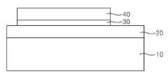
Translated fromKorean도 1a 내지 도 1d는 종래의 공정에 따른 발광 소자의 제조 방법을 설명하기 위한 단면도.1A to 1D are cross-sectional views illustrating a method of manufacturing a light emitting device according to a conventional process.
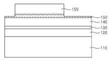
도 2a 내지 도 2f는 본 발명에 따른 발광 소자의 제조 방법을 설명하기 위한 단면도.2A to 2F are cross-sectional views illustrating a method of manufacturing a light emitting device according to the present invention.
도 3은 본 발명이 다른 실시예에 따른 발광 소자의 단면도.3 is a cross-sectional view of a light emitting device according to another embodiment of the present invention;
<도면의 주요 부분에 대한 부호의 설명><Explanation of symbols for the main parts of the drawings>
10, 110 : 기판20 : N-GaN층10, 110: substrate 20: N-GaN layer
30, 130 : 활성층40 : P-GaN층30, 130: active layer 40: P-GaN layer
50, 150, 160 : 투명전극60, 70, 170, 180 : 전극50, 150, 160:
120 : N형 반도체층140 : P형 반도체층120: N-type semiconductor layer 140: P-type semiconductor layer
155, 157 : 감광막 패턴165 : N형 금속패드
155, 157: Photosensitive film pattern 165: N-type metal pad
본 발명은 발광 소자 및 이의 제조 방법에 관한 것으로, 특히 N형 반도체층영역에서도 발광이 이루어지는 발광 소자에 관한 것이다.
The present invention relates to a light emitting device and a method of manufacturing the same, and more particularly, to a light emitting device that emits light in an N-type semiconductor layer region.
종래의 발광 소자는 사파이어 기판 상에 N-GaN층, 활성층 및 P-GaN층을 순차적으로 형성한다. 이때, N-GaN층 하부의 사파이어 기판이 부도체이기 때문에 N-GaN층 상부의 활성층과 P-GaN층의 일부를 식각하여 N-GaN층을 노출시켜 이를 외부 전원과 연결하였다. 또한, P-GaN층의 저항 성분이 매우 크기 때문에 P-GaN층 상부 표면에 균일하게 전압을 인가할 수 있도록 투명전극을 형성하였다.Conventional light emitting devices sequentially form an N-GaN layer, an active layer and a P-GaN layer on a sapphire substrate. At this time, since the sapphire substrate under the N-GaN layer is an insulator, a portion of the active layer and the P-GaN layer on the N-GaN layer are etched to expose the N-GaN layer and connected to an external power source. In addition, since the resistance component of the P-GaN layer is very large, a transparent electrode was formed to uniformly apply voltage to the upper surface of the P-GaN layer.
도 1a 내지 도 1d는 종래의 공정에 따른 발광 소자의 제조 방법을 설명하기 위한 단면도들이다.1A to 1D are cross-sectional views illustrating a method of manufacturing a light emitting device according to a conventional process.
도 1a를 참조하면, 사파이어(Al2O3) 기판(10) 상에 N-GaN층(20), 활성층(30) 및 P-GaN층(40)을 순차적으로 형성한다.Referring to FIG. 1A, an N-
도 1b를 참조하면, 소정의 패터닝 공정을 통해 P-GaN층(40) 및 활성층(30)의 일부를 제거하여 N-GaN층(20)의 일부를 노출시킨다. 이를 위해 P-GaN층(40) 상에 감광막 패턴(미도시)을 형성한 다음, 상기 감광막 패턴을 식각마스크로 하는 식각공정을 통해 P-GaN층(40) 및 활성층(30)을 제거한다. 이때, 감광막 패턴은 N 전극이 형성될 영역을 노출시키는 형상으로 형성한다. 상기 식각공정후 감광막 패턴을 제거한다.Referring to FIG. 1B, a portion of the N-
도 1c를 참조하면, P-GaN층(40) 상부에 투명전극(50)을 형성한다. 이를 위해 P-GaN층(40) 상부만을 노출하는 감광막 패턴을 형성한 다음, 노출된 영역에 투명전극(50)을 형성한다.Referring to FIG. 1C, a
도 1d를 참조하면, 노출된 N-GaN층(20) 상부에 N전극(60)을 형성하고, 투명전극(50) 상부에 P전극(70)을 형성한다.Referring to FIG. 1D, an
상술한 바와 같이 제조된 종래의 발광 소자는 외부 양자 효율이 10%이하로 매우 미비하다. 이는 활성층(30)에서 생성된 빛은 특정한 방향성이 없는 자발적 방출이다. 즉, PN접합부를 이루는 면에서 모든 방향으로 빛이 방출하게 된다. 하지만 실제적으로 반도체층 자체 및 층간의 결함에 의해 빛이 반사, 산란, 흡수되기 때문에 반도체층에 수직한 법선 방향으로만 빛이 외부로 방출된다. 하지만 법선방향으로 방출되는 빛의 양은 PN접합부의 계면을 따라 방출되는 빛의 양보다 적게 된다. 이러한 이유로 인해 발광 소자의 외부 양자 효율이 낮아지게 된다.
Conventional light emitting devices manufactured as described above have very low external quantum efficiency of 10% or less. This is the light generated in the
따라서, 본 발명은 상기의 문제점을 해결하기 위하여 P형 반도체층 뿐만 아니라 N형 반도체층을 통해서도 빛의 방출을 수행할 수 있고, N형 반도체층 상부에 소정의 거칠기를 주고, 그 상부에 투명전극을 형성하여 외부 양자 효율을 상승시킬 수 있는 발광 소자 및 이의 제조 방법을 제공함을 그 목적으로 한다.
Therefore, in order to solve the above problem, the present invention can perform light emission not only through the P-type semiconductor layer but also through the N-type semiconductor layer, and gives a predetermined roughness on the N-type semiconductor layer, and the transparent electrode thereon. It is an object of the present invention to provide a light emitting device and a method for manufacturing the same, which can increase the external quantum efficiency by forming a.
본 발명에 따른 기판 상에 N형 반도체층, P형 반도체층 및 제 1 투명전극층 을 형성하는 단계와, 소정 영역의 상기 제 1 투명전극층 및 상기 P형 반도체층을 제거하여 상기 N형 반도체층을 노출시키는 단계 및 노출된 상기 N형 반도체층 상에 제 2 투명전극층을 형성하되, 상기 P형 반도체층 및 상기 제 1 투명전극층과 소정간격 이격되도록 하는 단계를 포함하는 발광 소자의 제조 방법을 제공한다.Forming an N-type semiconductor layer, a P-type semiconductor layer, and a first transparent electrode layer on the substrate according to the present invention, and removing the first transparent electrode layer and the P-type semiconductor layer in a predetermined region to form the N-type semiconductor layer And forming a second transparent electrode layer on the exposed N-type semiconductor layer and spaced apart from the P-type semiconductor layer and the first transparent electrode layer by a predetermined distance. .
여기서, 상기 N형 반도체층과 상기 P형 반도체층 사이에 활성층이 형성된다. 상기의 N형 반도체층을 노출시키는 단계는, 상기 제 1 투명전극층 상에 소정의 감광막패턴을 형성하는 단계와, 상기 감광막 패턴을 식각마스크로 하는 제 1 식각공정을 실시하여 상기 제 1 투명전극층의 일부를 제거하는 단계와, 상기 감광막 패턴을 식각마스크로 하는 제 2 식각공정을 실시하여 잔류하는 상기 제 1 투명전극층, 상기 P형 반도체층 및 상기 활성층을 제거하여 상기 N형 반도체층을 노출시키되, 노출된 상기 N형 반도체층 상부 표면에 소정의 거칠기를 갖는 요철을 주는 단계 및 상기 감광막 패턴을 제거하는 단계를 포함한다.Here, an active layer is formed between the N-type semiconductor layer and the P-type semiconductor layer. The exposing the N-type semiconductor layer may include forming a predetermined photoresist pattern on the first transparent electrode layer and performing a first etching process using the photoresist pattern as an etching mask. Removing a portion of the photoresist pattern and performing a second etching process using the photoresist pattern as an etching mask to expose the N-type semiconductor layer by removing the remaining first transparent electrode layer, the P-type semiconductor layer, and the active layer; And providing a concave-convex surface having a predetermined roughness on the exposed upper surface of the N-type semiconductor layer, and removing the photoresist pattern.
그리고, 상기 제 1 투명전극층 상에 P전극을 형성하고, 상기 제 2 투명전극층 상에 N형 금속패드를 형성하는 단계를 더 포함한다. 상기 제 1 투명전극층 상에 P전극을 형성하는 단계와, 상기 N형 반도체층을 노출하는 단계 후, 상기 N형 반도체층 상에 N형 금속패드를 형성하는 단계를 더 포함한다.The method may further include forming a P electrode on the first transparent electrode layer and forming an N-type metal pad on the second transparent electrode layer. And forming an N-type metal pad on the N-type semiconductor layer after forming the P electrode on the first transparent electrode layer and exposing the N-type semiconductor layer.
또한, 본 발명에 따른, 기판과, 상기 기판 상에 형성된 N형 반도체층과, 상기 N형 반도체층의 소정 영역 상에 형성된 P형 반도체층과, 상기 P형 반도체층 상에 형성된 제 1 투명전극층과, 상기 제 1 투명전극층 상에 형성된 P전극 및 상기 N형 반도체층 상에 형성되고, 제 2 투명전극층을 포함하는 N전극을 포함하는 발광 소자를 제공한다.Further, according to the present invention, a substrate, an N-type semiconductor layer formed on the substrate, a P-type semiconductor layer formed on a predetermined region of the N-type semiconductor layer, and a first transparent electrode layer formed on the P-type semiconductor layer And a P electrode formed on the first transparent electrode layer and an N electrode formed on the N-type semiconductor layer and including a second transparent electrode layer.
이때, 상기 P형 반도체층이 형성되지 않은 상기 N형 반도체층 표면에 소정의 거칠기를 갖다. 그리고, 상기 P형 반도체층 하부에 형성된 활성층을 더 포함한다.At this time, the surface of the N-type semiconductor layer in which the P-type semiconductor layer is not formed has a predetermined roughness. And an active layer formed under the P-type semiconductor layer.
여기서, 상기 N전극은, 상기 N형 반도체층 상에 형성된 제 2 투명전극층 및 상기 제 2 투명전극층의 소정 영역 상에 형성된 금속패드를 포함한다. 뿐만 아니라, 상기 N전극은, 상기 N형 반도체층의 소정 영역 상에 형성된 금속패드 및 상기 금속패드를 포함한 상기 N형 반도체층 상에 형성된 제 2 투명전극층을 포함한다.
Here, the N electrode includes a second transparent electrode layer formed on the N-type semiconductor layer and a metal pad formed on a predetermined region of the second transparent electrode layer. In addition, the N electrode includes a metal pad formed on a predetermined region of the N type semiconductor layer and a second transparent electrode layer formed on the N type semiconductor layer including the metal pad.
이하, 첨부된 도면을 참조하여 본 발명의 실시예를 더욱 상세히 설명하기로 한다. 그러나 본 발명은 이하에서 개시되는 실시예에 한정되는 것이 아니라 서로 다른 다양한 형태로 구현될 것이며, 단지 본 실시예들은 본 발명의 개시가 완전하도록 하며, 통상의 지식을 가진 자에게 발명의 범주를 완전하게 알려주기 위해 제공되는 것이다. 도면상에서 동일 부호는 동일한 요소를 지칭한다.
Hereinafter, embodiments of the present invention will be described in detail with reference to the accompanying drawings. It will be apparent to those skilled in the art that the present invention may be embodied in many different forms and should not be construed as limited to the embodiments set forth herein. Rather, these embodiments are provided so that this disclosure will be thorough and complete, It is provided to let you know. Like numbers refer to like elements in the figures.
도 2a 내지 도 2f는 본 발명에 따른 발광 소자의 제조 방법을 설명하기 위한 단면도들이다.2A to 2F are cross-sectional views illustrating a method of manufacturing a light emitting device according to the present invention.
도 2a를 참조하면, 사파이어 기판(110) 상에 N형 반도체층(120), 활성층(130), P형 반도체층(140) 및 제 1 투명전극층(150)을 순차적으로 형성한다.Referring to FIG. 2A, the N-
이때, 사파이어 기판(110) 대신 SiC, ZnO, Si, GaAs, GaP, LiAl2O3, BN, AlN 및 GaN 중 적어도 어느 하나의 기판을 사용할 수 있다. 또한, 기판(110) 상에 N형 반도체층(120) 형성시 완충역할을 하는 버퍼층(미도시)을 더 형성할 수 있다.In this case, at least one of SiC, ZnO, Si, GaAs, GaP, LiAl 2 O 3, BN, AlN, and GaN may be used instead of the
상기의 N형 반도체층(120)은 N형 불순물이 주입된 질화갈륨(GaN)막을 사용하는 것이 바람직하고, 이에 한정되지 않고 다양한 반도체 성질의 물질층이 가능하다. 본 실시예에서는 N 형 AlxGa1-xN(0≤x≤1)막을 포함하는 N형 반도체층(120)을 형성한다.The N-
더욱이, P형 반도체층(140) 또한 P형 불순물이 주입된 질화갈륨막을 사용한다. 본 실시예에서는 P형 AlxGa1-xN(0≤x≤1)막을 포함하는 P형 반도체층(140)을 형성한다. 이뿐 아니라 상기 반도체층 막으로 InGaN막을 사용할 수 있다. 또한 상기의 N형 반도체층(120) 및 P형 반도체층(140)은 다층막으로 형성할 수도 있다. 상기에서 N형의 불순물로는 Si를 사용하고, P형의 불순물로는 InGaAlP를 사용할 경우에는 Zn을 사용하고, 질화물계일때는 Mg를 사용한다.In addition, the P-
또한, 활성층(13)으로는 N형 AlxGa1-xN(0≤x≤1) 막 위에 양자우물층과 장벽층이 반복적으로 형성된 다층막을 사용한다. 상기의 장벽층과 우물층은 2원 화합물인 GaN, InN, AlN 등을 사용할 수 있고, 3원 화합물 InxGa1-xN(0≤x≤1), AlxGa1-xN(0≤x≤1) 등을 사용할 수 있고, 4원 화합물 AlxInyGa1-x-yN(0≤x+y≤1)을 사용할 수 있다. 물론 상기의 2원 내지 4원 화합물에 소정의 불순물을 주입하여 N형 반도체층(120) 및 P형 반도체층(140)을 형성할 수도 있다. 이때, 우물층과 장벽층의 조성 및 두께를 제어하여 목표로 하는 파장의 빛을 얻을 수 있다.As the active layer 13, a multilayer film in which a quantum well layer and a barrier layer are repeatedly formed on an N-type Alx Ga1-x N (0≤x≤1) film is used. As the barrier layer and the well layer, binary compounds such as GaN, InN, and AlN may be used, and ternary compounds Inx Ga1-x N (0 ≦x ≦1 ) and Alx Ga1-x N (0 ≤x ≤ 1) and the like, and a quaternary compound Alx Iny Ga1-xy N (0 ≦ x + y ≦ 1) may be used. Of course, the N-
그리고, 제 1 투명전극층(150)으로는 ITO(Indium Tin Oxide)를 포함한 다양한 물질막을 사용한다. 바람직하게는 투명도가 50 내지 100%인 물질을 제 1 투명전극층(150)으로 사용한다.In addition, various material films including indium tin oxide (ITO) are used as the first
상술한 물질층들은 유기금속 화학 증착법(MOCVD; Metal Organic Chemical Vapor Deposition), 분자선 성장법(MBE; Molecular Beam Epitaxy), 수소화물 기상 성장법(HVPE; Hydride Vapor Phase Epitaxy) 등을 포함한 다양한 증착 및 성장방법을 통해 형성된다.The above-described material layers can be deposited and grown in various ways including metal organic chemical vapor deposition (MOCVD), molecular beam growth (MBE), hydride vapor phase epitaxy (HVPE), and the like. Is formed through the method.
도 2b 및 도 2c를 참조하면, 제 1 투명전극층(150), P형 반도체층(140) 및 활성층(130)의 일부를 제거하여 N형 반도체층(120)의 일부를 노출시키되, 노출된 N형 반도체층(120) 표면에 소정의 거칠기를 갖는 요철을 형성한다. N형 반도체층(120) 요철의 거칠기(Ra)는 50 내지 50000Å인 것이 바람직하다.2B and 2C, a portion of the N-
이를 위해, 먼저 제 1 투명전극층(150) 상에 감광막을 도포한 다음, 마스크를 이용한 사진식각 공정을 통해 제 1 감광막 패턴(155)을 형성한다. 이때, 제 1 감광막 패턴(155)은 N형 전극이 형성될 영역은 개방하고 나머지 영역은 차폐하는 형상으로 형성한다. 즉, 도면에서 보여지는 바와 같이 P형 반도체층(140)의 양측 영역을 개방하도록 형성하는 것이 바람직하다. 또한, 도시되지는 않았지만, 상부에서 제 1 감광막 패턴(155)을 바라볼 경우, P형 반도체층(140) 둘레에 소폭 노출되어 있고, 직사각형의 발광소자의 일 꼭지점 영역에 소정의 폭(면적)을 갖는 영역이 개방되어 있다.To this end, first, a photosensitive film is coated on the first
이후, 제 1 감광막 패턴(155)을 식각마스크로 하는 제 1 식각공정을 실시하 여 노출된 제 1 투명전극층(150)의 일부를 제거한다. 이때, 제 1 식각공정시 제거되지 않고 잔류하는 제 1 투명전극층(150)의 두께는 1 내지 500Å이 되도록 한다. 계속적으로 제 2 식각공정을 통해 잔류하는 제 1 투명전극층(150)과, P형 반도체층(140) 및 활성층(130)을 제거하여 N형 반도체층(120)을 노출시키게 되면, 노출된 N형 반도체층(120) 표면에 소정의 요철이 형성된다.Thereafter, a part of the exposed first
상기 제 1 식각공정은 습식 식각 방법을 이용하고 제 2 식각공정은 건식 식각 방법을 이용하는 것이 바람직하다. 즉, 습식 식각을 통해 제 1 투명전극층(150)의 전체를 제거하지 않은 상태에서 건식 식각을 통해 잔류하는 제 1 투명전극층(150), P형 반도체층(140) 및 활성층(130)을 제거하게 되면 N형 반도체층(120)의 표면이 거칠어지게 된다. 이는 건식식각시 제 1 투명전극층(150)이 어느 정도의 배리어 역할을 하게 되어 하부의 막층이 매끄럽게 식각되지 못하고 그 표면에 소정의 요철과 같은 거칠기가 있게 된다.It is preferable that the first etching process uses a wet etching method and the second etching process uses a dry etching method. That is, the first
요철이 형성된 거친 표면의 상태를 다져주는 반응성 가스를 투입하여 광출력을 더 향상 시킬 수 있다. 이때, 반응성 가스로는 아르곤(Ar) 가스를 사용한다. 즉. 이온화 에너지를 이용한 물리적 식각인 플라즈마 식각을 실시한다.The light output can be further improved by adding a reactive gas to reduce the condition of the rough surface on which the unevenness is formed. At this time, argon (Ar) gas is used as the reactive gas. In other words. Plasma etching, which is physical etching using ionization energy, is performed.
상술한 제 2 식각공정시 N형 반도체층(120)의 일부도 함께 식각될 수 있다. 상술한 바와 같이 발광 소자의 노출된 N형 반도체층(120)의 표면에 소정의 요철을 주어서 N형 반도체층(120)에서도 발광을 하는 것과 같은 현상을 볼 수 있으며, 이를 통해 발광 소자의 양자 효율을 40 내지 70%정도 향상시킬 수 있다.A portion of the N-
도 2d 및 도 2e를 참조하면, 제 1 감광막 패턴(155)을 제거한 다음, 소정의 세정공정을 실시한다. 이후, 노출된 N형 반도체층(120)의 소정영역에 제 2 투명전극층(160)을 형성한다.2D and 2E, after removing the
이를 위해 전체 구조 상에 감광막을 도포한 다음, 마스크를 이용한 사진식각공정을 실시하여 N형 반도체층(120)의 일부를 노출시키는 제 2 감광막 패턴(157)을 형성한다. 상기의 제 2 감광막 패턴(157)은 노출된 N형 반도체층(120) 영역 중에서 활성층(130)과 인접한 영역을 제외한 모든 영역을 노출시키는 형상으로 형성한다. 물론 이에 한정되지 않고, 노출된 N형 반도체층(120)의 소정영역을 노출시키되, 활성층(130), P형 반도체층(140) 및 제 1 투명전극층(150)이 노출되지 않도록 한다. 즉, 도 2d에서와 같이 활성층(130), P형 반도체층(140) 및 제 1 투명전극층(150)을 감싸는 형상의 제 2 감광막 패턴(157)을 형성한다.To this end, a photoresist film is coated on the entire structure, and then a photolithography process using a mask is performed to form a
이후, 제 2 감광막 패턴(157)에 의해 노출된 N형 반도체층(120) 상에 제 2 투명전극층(160)을 형성한다. 이때, 제 2 투명전극층(160)은 앞서 설명한 제 1 투명전극층(150)과 동일한 물질층을 사용한다. 소정의 스트립 공정을 실시하여 제 2 감광막 패턴(157)을 제거한다.Thereafter, a second
이때, 본 발명은 제 1 감광막 패턴(155)을 제거하지 않은 상태에서 제 2 감광막 패턴(157)을 형성할 수 있다. 또한, 감광막 패턴이 아니 별도의 배리어 기능을 수행할 수 있는 다양한 물질막을 감광막 패턴 대신 사용할 수 있다.In this case, the second
도 2f를 참조하면, 제 1 투명전극층(150) 상의 소정영역에 P전극(180)을 형성하고, 제 2 투명전극(160) 상의 소정 영역에 N형 금속 패드(165)를 형성하여 N전극(170)을 형성한다.Referring to FIG. 2F, a
이를 위해 전체 구조 상에 전극 형성을 위한 마스크 패턴을 형성한다. 마스크 패턴은 P형 반도체층(130) 상에 형성된 제 1 투명전극층(150)의 일부를 노출시키고, N형 반도체층(120) 상에 형성된 제 2 투명전극층(160)의 일부를 노출시킨다. 물론, 마스크 패턴은 제 1 투명전극층(150) 전체와 제 2 투명전극층(160) 전체를 노출시킬 수도 있다. 이후, 소정의 금속층을 전체 구조 상에 형성한 다음, 개방된 제 1 및 제 2 투명전극층(150, 160) 상부를 제외한 영역의 금속층과 마스크 패턴을 제거하여 P전극(180)을 형성하고, 제 2 투명전극층(160)과 N형 금속패드(165)로 구성된 N전극(170)을 형성한다. 물론 상술한 공정에 한정되지 않고, 다양한 금속층 증착 방법을 통해 N전극(170) 및 P전극(180)을 형성할 수 있다.To this end, a mask pattern for forming an electrode is formed on the entire structure. The mask pattern exposes a portion of the first
상술한 공정에 한정되지 않고, 본 발명에서는 N형 반도체층(120) 상에 형성된 제 2 투명전극층(160)을 N전극(170)으로 사용할 수 있다. 즉, N형 반도체층(120)으로 사용하는 N-GaN층은 N타입이고, 제 2 투명전극(160)으로 사용하는 ITO역시 N타입이다. ITO는 전기 전도성이 우수할 뿐만 아니라 굴절율과 광투과율면에서 우수하기 때문에 N전극 메탈로 대신하는 역할을 수행할 수 있다. 즉, 기존의 N 금속 보다 ITO가 효율이 더 우수하다. 그리고, 상기 ITO의 굴절율 n은 1.9 내지 2.0이다.In the present invention, the second
도 3은 본 발명이 다른 실시예에 따른 발광 소자의 단면도이다.3 is a cross-sectional view of a light emitting device according to another embodiment of the present invention.
도 3을 참조하면, 본 발명의 다른 실시예에 따른 발광 소자는 N형 반도체층 (120) 상에 N형 금속 패드(165)를 형성한 다음 그 상부에 제 2 투명전극층(160)을 형성하여 N전극(170)을 형성한다.Referring to FIG. 3, in the light emitting device according to another embodiment of the present invention, an N-
즉, 기판(110) 상에 버퍼층(미도시), N형 반도체층(120), 활성층(130), P형 반도체층(140), 제 1 투명전극층(150)을 형성한다. 소정 영역의 제 1 투명전극층(150)을 식각하되, 제 1 투명전극층(150)을 소정 두께 잔류시킨다. 이후, 계속적인 식각을 실시하여 소정 영역에 소정 두께로 잔류하는 제 1 투명전극층(150), P형 반도체층(140) 및 활성층(130)을 제거하여 N형 반도체층(120)을 노출시킨다. 이때, 상술한 공정에 의해 N형 반도체층(120) 표면에 소정의 거칠기를 갖는 요철이 형성된다.That is, a buffer layer (not shown), an N-
이후, N형 반도체층(120) 상에 N형 금속패드(165)를 형성한다. 이때, N형 금속패드(165)와 함께 P전극(180)을 동시에 형성할 수도 있고, P전극(180)을 먼저 형성한 다음, N형 금속패드(165)를 형성할 수 있다. 또한, N형 금속패드(165)의 형성후, P전극(180)을 형성할 수도 있다.Thereafter, an N-
다음으로, N형 금속 패드(165)가 형성된 N형 반도체층(120) 상에 제 2 투명전극(160)을 형성한다. 제 2 투명전극(160)은 활성층(130)과 소정간격 이격되도록 형성하고, N형 금속 패드(165)을 감싸는 형상으로 형성한다. 또한, 제 2 투명전극(160) 형성후, P전극(180)을 형성할 수도 있다. 이때, N패드와 접속된 N형 금속패드(165)영역의 일부가 개방되도록 제 2 투명전극(160)의 일부를 제거할 수 있다. 즉, 제 2 투명전극(160)으로 N형 금속패드(165)를 감싸도록 형성하되 후속 패키징 공정의 와이어 본딩영역에 해당하는 N형 금속패드(165) 상부를 개방한다. 이때 소정의 패터닝 공정을 통해 제 2 투명전극(160)의 일부를 제거하여 이를 수행할 수 있다.Next, the second
이하, 상술한 설명에 의해 형성된 발광 소자에 관해 설명한다.Hereinafter, the light emitting element formed by the above-mentioned description is demonstrated.
도 2 및 도 3에서 도시된 바와 같이 본 발명의 발광 소자는 기판(110)과, 기판(110) 상에 형성된 N형 반도체층(120)과, N형 반도체층(120)의 소정 영역 상에 형성된 P형 반도체층(140)과, P형 반도체층(140) 상에 형성된 제 1 투명전극층(150)과, 제 1 투명전극층(150) 상에 형성된 P전극(180)과, N형 반도체층(120) 상에 형성된 N전극(170)을 포함하되, P형 반도체층(140)이 형성되지 않은 N형 반도체층(120) 표면에 소정의 거칠기를 갖는다. 이때, P형 반도체층(140) 하부에는 활성층(130)이 더 형성된다. 또한, N형 반도체층(120)과 기판(110) 사이에는 버퍼층(미도시)이 더 형성된다. N전극(170)으로는 제 2 투명전극층(160)을 사용한다. 또한, N전극(170)으로는 N형 반도체층(120) 상에 형성된 제 2 투명전극층(160)과, 제 2 투명전극층(160)의 소정 영역 상에 형성된 N형 금속패드(165)를 사용할 수도 있다. 또한, N전극(170)으로 N형 반도체층(120)의 소정 영역 상에 형성된 N형 금속패드(165)와, 상기 N형 금속패드(165)를 포함한 N형 반도체층(120) 상에 형성된 제 2 투명전극층(160)을 사용할 수도 있다.As shown in FIG. 2 and FIG. 3, the light emitting device of the present invention includes a
본 발명의 ITO 후면에 0.001㎛ 내지 2.0㎛두께의 반사금속(Reflector metal)층을 증착 또는 성장시키는 것이 바람직하다.It is preferable to deposit or grow a reflective metal layer having a thickness of 0.001 μm to 2.0 μm on the back surface of the ITO of the present invention.
이를 통해 기존의 에미션 영역(Emission Area)뿐만 아니라 식각된 N형 반도체영역까지 발광 면적을 늘려 광출력을 극대화 할 수 있다.
Through this, it is possible to maximize the light output by increasing the light emitting area not only the existing emission area but also the etched N-type semiconductor area.
상술한 바와 같이, 본 발명은 발광 소자의 노출된 N형 반도체층 상에 투명전극층을 형성하고, 이를 N전극으로 사용함으로써, 발광면적을 확대할 수 있고, 광출력을 극대화 할 수 있다. As described above, in the present invention, by forming a transparent electrode layer on the exposed N-type semiconductor layer of the light emitting device, and using it as the N electrode, the light emitting area can be enlarged and the light output can be maximized.
또한, N형 반도체층 표면에 소정의 거칠기를 갖는 요철을 형성하여 N형 반도체층으로도 발광이 이루어지도록 하여 발광 소자의 양자 효율을 향상시킬 수 있다.
In addition, the quantum efficiency of the light emitting device can be improved by forming irregularities having a predetermined roughness on the surface of the N-type semiconductor layer so that light can be emitted from the N-type semiconductor layer.
Claims (11)
Translated fromKoreanPriority Applications (1)
| Application Number | Priority Date | Filing Date | Title |
|---|---|---|---|
| KR1020040113119AKR101138973B1 (en) | 2004-12-27 | 2004-12-27 | Luminescence device and method of manufacturing the same |
Applications Claiming Priority (1)
| Application Number | Priority Date | Filing Date | Title |
|---|---|---|---|
| KR1020040113119AKR101138973B1 (en) | 2004-12-27 | 2004-12-27 | Luminescence device and method of manufacturing the same |
Publications (2)
| Publication Number | Publication Date |
|---|---|
| KR20060074390A KR20060074390A (en) | 2006-07-03 |
| KR101138973B1true KR101138973B1 (en) | 2012-04-25 |
Family
ID=37167156
Family Applications (1)
| Application Number | Title | Priority Date | Filing Date |
|---|---|---|---|
| KR1020040113119AExpired - Fee RelatedKR101138973B1 (en) | 2004-12-27 | 2004-12-27 | Luminescence device and method of manufacturing the same |
Country Status (1)
| Country | Link |
|---|---|
| KR (1) | KR101138973B1 (en) |
Cited By (1)
| Publication number | Priority date | Publication date | Assignee | Title |
|---|---|---|---|---|
| US9142730B2 (en) | 2013-09-25 | 2015-09-22 | Samsung Electronics Co., Ltd. | Method of manufacturing semiconductor light emitting device |
Families Citing this family (1)
| Publication number | Priority date | Publication date | Assignee | Title |
|---|---|---|---|---|
| KR101530876B1 (en) | 2008-09-16 | 2015-06-23 | 삼성전자 주식회사 | Light emitting device with increased light emitting amount, light emitting device including same, method of manufacturing light emitting device and light emitting device |
Citations (3)
| Publication number | Priority date | Publication date | Assignee | Title |
|---|---|---|---|---|
| JPH10173222A (en)* | 1996-12-06 | 1998-06-26 | Rohm Co Ltd | Manufacture of semiconductor light emitting element |
| JP2004165433A (en)* | 2002-11-13 | 2004-06-10 | ▲さん▼圓光電股▲ふん▼有限公司 | Light emitting diode having low resistance layer |
| KR100452749B1 (en) | 2003-08-12 | 2004-10-15 | 에피밸리 주식회사 | III-Nitride compound semiconductor light emitting device with fine and high density surface gratings |
- 2004
- 2004-12-27KRKR1020040113119Apatent/KR101138973B1/ennot_activeExpired - Fee Related
Patent Citations (3)
| Publication number | Priority date | Publication date | Assignee | Title |
|---|---|---|---|---|
| JPH10173222A (en)* | 1996-12-06 | 1998-06-26 | Rohm Co Ltd | Manufacture of semiconductor light emitting element |
| JP2004165433A (en)* | 2002-11-13 | 2004-06-10 | ▲さん▼圓光電股▲ふん▼有限公司 | Light emitting diode having low resistance layer |
| KR100452749B1 (en) | 2003-08-12 | 2004-10-15 | 에피밸리 주식회사 | III-Nitride compound semiconductor light emitting device with fine and high density surface gratings |
Cited By (1)
| Publication number | Priority date | Publication date | Assignee | Title |
|---|---|---|---|---|
| US9142730B2 (en) | 2013-09-25 | 2015-09-22 | Samsung Electronics Co., Ltd. | Method of manufacturing semiconductor light emitting device |
Also Published As
| Publication number | Publication date |
|---|---|
| KR20060074390A (en) | 2006-07-03 |
Similar Documents
| Publication | Publication Date | Title |
|---|---|---|
| JP4994758B2 (en) | Gallium nitride semiconductor light emitting device and method for manufacturing the same | |
| US7919784B2 (en) | Semiconductor light-emitting device and method for making same | |
| KR101000311B1 (en) | Semiconductor light emitting device and manufacturing method thereof | |
| KR101258582B1 (en) | Nano rod light emitting device | |
| EP1929545A1 (en) | Semiconductor light-emitting device and method for making same | |
| KR20110055110A (en) | Semiconductor light emitting device and manufacturing method thereof | |
| KR101123010B1 (en) | semi-conductor light emitting device and manufacturing method thereof | |
| KR20130025856A (en) | Nano rod light emitting device | |
| KR101239852B1 (en) | GaN compound semiconductor light emitting element | |
| KR101203137B1 (en) | GaN compound semiconductor light emitting element and method of manufacturing the same | |
| KR101077769B1 (en) | Luminescence device and method of manufacturing the same | |
| KR101138943B1 (en) | luminescence device and Method of manufacturing the same | |
| KR20110043282A (en) | Light emitting device and manufacturing method | |
| KR100830643B1 (en) | Manufacturing method of light emitting device | |
| KR101138950B1 (en) | Luminescence device | |
| KR101138973B1 (en) | Luminescence device and method of manufacturing the same | |
| KR101158074B1 (en) | luminescence device | |
| KR100663910B1 (en) | Light emitting device and manufacturing method thereof | |
| KR101267437B1 (en) | Light emitting diodes and method for fabricating the same | |
| KR100756842B1 (en) | Light-emitting diode having light extraction columns and method of manufacturing same | |
| KR101186685B1 (en) | Luminescence device | |
| KR20090108506A (en) | Group III-nitride semiconductor light emitting diode device and method for manufacturing same | |
| KR100905859B1 (en) | Nitride semiconductor light emitting device and manufacturing method thereof | |
| KR101229814B1 (en) | luminescence device | |
| KR100616414B1 (en) | Light emitting element |
Legal Events
| Date | Code | Title | Description |
|---|---|---|---|
| PA0109 | Patent application | St.27 status event code:A-0-1-A10-A12-nap-PA0109 | |
| PG1501 | Laying open of application | St.27 status event code:A-1-1-Q10-Q12-nap-PG1501 | |
| P22-X000 | Classification modified | St.27 status event code:A-2-2-P10-P22-nap-X000 | |
| A201 | Request for examination | ||
| PA0201 | Request for examination | St.27 status event code:A-1-2-D10-D11-exm-PA0201 | |
| R17-X000 | Change to representative recorded | St.27 status event code:A-3-3-R10-R17-oth-X000 | |
| E902 | Notification of reason for refusal | ||
| PE0902 | Notice of grounds for rejection | St.27 status event code:A-1-2-D10-D21-exm-PE0902 | |
| T11-X000 | Administrative time limit extension requested | St.27 status event code:U-3-3-T10-T11-oth-X000 | |
| E13-X000 | Pre-grant limitation requested | St.27 status event code:A-2-3-E10-E13-lim-X000 | |
| P11-X000 | Amendment of application requested | St.27 status event code:A-2-2-P10-P11-nap-X000 | |
| P13-X000 | Application amended | St.27 status event code:A-2-2-P10-P13-nap-X000 | |
| E701 | Decision to grant or registration of patent right | ||
| PE0701 | Decision of registration | St.27 status event code:A-1-2-D10-D22-exm-PE0701 | |
| GRNT | Written decision to grant | ||
| PR0701 | Registration of establishment | St.27 status event code:A-2-4-F10-F11-exm-PR0701 | |
| PR1002 | Payment of registration fee | St.27 status event code:A-2-2-U10-U11-oth-PR1002 Fee payment year number:1 | |
| PG1601 | Publication of registration | St.27 status event code:A-4-4-Q10-Q13-nap-PG1601 | |
| R18-X000 | Changes to party contact information recorded | St.27 status event code:A-5-5-R10-R18-oth-X000 | |
| R18-X000 | Changes to party contact information recorded | St.27 status event code:A-5-5-R10-R18-oth-X000 | |
| PN2301 | Change of applicant | St.27 status event code:A-5-5-R10-R13-asn-PN2301 St.27 status event code:A-5-5-R10-R11-asn-PN2301 | |
| PR1001 | Payment of annual fee | St.27 status event code:A-4-4-U10-U11-oth-PR1001 Fee payment year number:4 | |
| PR1001 | Payment of annual fee | St.27 status event code:A-4-4-U10-U11-oth-PR1001 Fee payment year number:5 | |
| FPAY | Annual fee payment | Payment date:20170308 Year of fee payment:6 | |
| PR1001 | Payment of annual fee | St.27 status event code:A-4-4-U10-U11-oth-PR1001 Fee payment year number:6 | |
| P22-X000 | Classification modified | St.27 status event code:A-4-4-P10-P22-nap-X000 | |
| PR1001 | Payment of annual fee | St.27 status event code:A-4-4-U10-U11-oth-PR1001 Fee payment year number:7 | |
| P22-X000 | Classification modified | St.27 status event code:A-4-4-P10-P22-nap-X000 | |
| LAPS | Lapse due to unpaid annual fee | ||
| PC1903 | Unpaid annual fee | St.27 status event code:A-4-4-U10-U13-oth-PC1903 Not in force date:20190417 Payment event data comment text:Termination Category : DEFAULT_OF_REGISTRATION_FEE | |
| PC1903 | Unpaid annual fee | St.27 status event code:N-4-6-H10-H13-oth-PC1903 Ip right cessation event data comment text:Termination Category : DEFAULT_OF_REGISTRATION_FEE Not in force date:20190417 | |
| P22-X000 | Classification modified | St.27 status event code:A-4-4-P10-P22-nap-X000 |