KR101138075B1 - Method for Forming Dual Damascene Pattern - Google Patents
Method for Forming Dual Damascene PatternDownload PDFInfo
- Publication number
- KR101138075B1 KR101138075B1KR1020040115260AKR20040115260AKR101138075B1KR 101138075 B1KR101138075 B1KR 101138075B1KR 1020040115260 AKR1020040115260 AKR 1020040115260AKR 20040115260 AKR20040115260 AKR 20040115260AKR 101138075 B1KR101138075 B1KR 101138075B1
- Authority
- KR
- South Korea
- Prior art keywords
- hard mask
- mask layer
- forming
- pattern
- layer
- Prior art date
- Legal status (The legal status is an assumption and is not a legal conclusion. Google has not performed a legal analysis and makes no representation as to the accuracy of the status listed.)
- Expired - Fee Related
Links
Images


Classifications
- H—ELECTRICITY
- H01—ELECTRIC ELEMENTS
- H01L—SEMICONDUCTOR DEVICES NOT COVERED BY CLASS H10
- H01L21/00—Processes or apparatus adapted for the manufacture or treatment of semiconductor or solid state devices or of parts thereof
- H01L21/70—Manufacture or treatment of devices consisting of a plurality of solid state components formed in or on a common substrate or of parts thereof; Manufacture of integrated circuit devices or of parts thereof
- H01L21/71—Manufacture of specific parts of devices defined in group H01L21/70
- H01L21/768—Applying interconnections to be used for carrying current between separate components within a device comprising conductors and dielectrics
- H01L21/76801—Applying interconnections to be used for carrying current between separate components within a device comprising conductors and dielectrics characterised by the formation and the after-treatment of the dielectrics, e.g. smoothing
- H01L21/76802—Applying interconnections to be used for carrying current between separate components within a device comprising conductors and dielectrics characterised by the formation and the after-treatment of the dielectrics, e.g. smoothing by forming openings in dielectrics
- H01L21/76807—Applying interconnections to be used for carrying current between separate components within a device comprising conductors and dielectrics characterised by the formation and the after-treatment of the dielectrics, e.g. smoothing by forming openings in dielectrics for dual damascene structures
- H—ELECTRICITY
- H01—ELECTRIC ELEMENTS
- H01L—SEMICONDUCTOR DEVICES NOT COVERED BY CLASS H10
- H01L21/00—Processes or apparatus adapted for the manufacture or treatment of semiconductor or solid state devices or of parts thereof
- H01L21/02—Manufacture or treatment of semiconductor devices or of parts thereof
- H01L21/04—Manufacture or treatment of semiconductor devices or of parts thereof the devices having potential barriers, e.g. a PN junction, depletion layer or carrier concentration layer
- H01L21/18—Manufacture or treatment of semiconductor devices or of parts thereof the devices having potential barriers, e.g. a PN junction, depletion layer or carrier concentration layer the devices having semiconductor bodies comprising elements of Group IV of the Periodic Table or AIIIBV compounds with or without impurities, e.g. doping materials
- H01L21/30—Treatment of semiconductor bodies using processes or apparatus not provided for in groups H01L21/20 - H01L21/26
- H01L21/31—Treatment of semiconductor bodies using processes or apparatus not provided for in groups H01L21/20 - H01L21/26 to form insulating layers thereon, e.g. for masking or by using photolithographic techniques; After treatment of these layers; Selection of materials for these layers
- H01L21/3105—After-treatment
- H01L21/311—Etching the insulating layers by chemical or physical means
- H01L21/31105—Etching inorganic layers
- H01L21/31111—Etching inorganic layers by chemical means
- H01L21/31116—Etching inorganic layers by chemical means by dry-etching
- H—ELECTRICITY
- H01—ELECTRIC ELEMENTS
- H01L—SEMICONDUCTOR DEVICES NOT COVERED BY CLASS H10
- H01L21/00—Processes or apparatus adapted for the manufacture or treatment of semiconductor or solid state devices or of parts thereof
- H01L21/02—Manufacture or treatment of semiconductor devices or of parts thereof
- H01L21/04—Manufacture or treatment of semiconductor devices or of parts thereof the devices having potential barriers, e.g. a PN junction, depletion layer or carrier concentration layer
- H01L21/18—Manufacture or treatment of semiconductor devices or of parts thereof the devices having potential barriers, e.g. a PN junction, depletion layer or carrier concentration layer the devices having semiconductor bodies comprising elements of Group IV of the Periodic Table or AIIIBV compounds with or without impurities, e.g. doping materials
- H01L21/30—Treatment of semiconductor bodies using processes or apparatus not provided for in groups H01L21/20 - H01L21/26
- H01L21/31—Treatment of semiconductor bodies using processes or apparatus not provided for in groups H01L21/20 - H01L21/26 to form insulating layers thereon, e.g. for masking or by using photolithographic techniques; After treatment of these layers; Selection of materials for these layers
- H01L21/3105—After-treatment
- H01L21/311—Etching the insulating layers by chemical or physical means
- H01L21/31144—Etching the insulating layers by chemical or physical means using masks
- H—ELECTRICITY
- H01—ELECTRIC ELEMENTS
- H01L—SEMICONDUCTOR DEVICES NOT COVERED BY CLASS H10
- H01L21/00—Processes or apparatus adapted for the manufacture or treatment of semiconductor or solid state devices or of parts thereof
- H01L21/70—Manufacture or treatment of devices consisting of a plurality of solid state components formed in or on a common substrate or of parts thereof; Manufacture of integrated circuit devices or of parts thereof
- H01L21/71—Manufacture of specific parts of devices defined in group H01L21/70
- H01L21/768—Applying interconnections to be used for carrying current between separate components within a device comprising conductors and dielectrics
- H01L21/76801—Applying interconnections to be used for carrying current between separate components within a device comprising conductors and dielectrics characterised by the formation and the after-treatment of the dielectrics, e.g. smoothing
- H01L21/76835—Combinations of two or more different dielectric layers having a low dielectric constant
Landscapes
- Engineering & Computer Science (AREA)
- Microelectronics & Electronic Packaging (AREA)
- Condensed Matter Physics & Semiconductors (AREA)
- General Physics & Mathematics (AREA)
- Manufacturing & Machinery (AREA)
- Computer Hardware Design (AREA)
- Physics & Mathematics (AREA)
- Power Engineering (AREA)
- Chemical & Material Sciences (AREA)
- Chemical Kinetics & Catalysis (AREA)
- General Chemical & Material Sciences (AREA)
- Inorganic Chemistry (AREA)
- Internal Circuitry In Semiconductor Integrated Circuit Devices (AREA)
Abstract
Translated fromKoreanDescription
Translated fromKorean도 1a 및 도 1d는 종래 이중 다마신 패턴 형성 방법을 도시한 공정 단면도.1A and 1D are cross-sectional views illustrating a method of forming a conventional dual damascene pattern.
도 2a 내지 도 2l은 본 발명의 이중 다마신 패턴 형성 방법을 도시한 공정 단면도.2A to 2L are cross-sectional views illustrating a method for forming a dual damascene pattern of the present invention.
< 도면의 주요 부분에 대한 간단한 설명 ><Brief description of the main parts of the drawing>
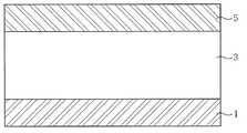
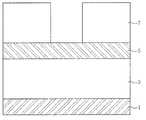
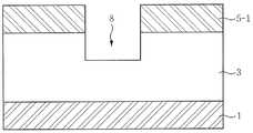
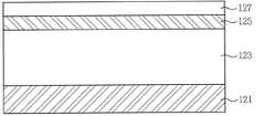
1, 121 : 피식각층3, 123 : 비아홀용 다공성 저유전막1, 121:
5 : 하드마스크막 5-1 : 하드마스크막 패턴5: hard mask film 5-1: hard mask film pattern
7 : 포토레지스트 패턴8, 130 : 금속배선용 비아홀7
125 : 제 1 하드마스크막125-1 : 제 1 하드마스크 패턴125: first hard mask film 125-1: first hard mask pattern
127 : 제 2 하드마스크막127-1 : 제 2 하드마스크막 패턴127: second hard mask film 127-1: second hard mask film pattern
129 : 제 1 포토레지스트 패턴131 : 트렌치용 다공성 저유전막129: first photoresist pattern 131: porous low dielectric film for trench
133 : 제 3 하드마스크막133-1 : 제 3 하드마스크막 패턴133: third hard mask film 133-1: third hard mask film pattern
135 : 제 4 하드마스크막135-1 : 제 4 하드마스크막 패턴135: fourth hard mask film 135-1: fourth hard mask film pattern
137 : 제 2 포토레지스트 패턴139 : 금속배선용 트렌치137: second photoresist pattern 139: trench for metal wiring
141 : 구리층143 : 구리 배선141: copper layer 143: copper wiring
본 발명은 이중 다마신(dual damascene)패턴 형성 방법에 관한 것으로, 보다 상세하게는 금속간 유전체 물질(inter-metal dielectrics)중 하나인 다공성 저유전막(porous low-K dielectric)을 사용하여 구리 배선을 형성하는 이중 다마신(dual damascene) 공정 시에, 비아홀 및 트렌치를 형성하기 위한 각각의 식각 공정에서 이중 하드마스크막(dual hard mask film)을 사용함으로써, 후속 공정인 O2 애싱 (O2 base ashing) 공정에 의한 상기 다공성 저유전막의 손상(damage)을 방지할 수 있는 이중 다마신 패턴 형성 방법에 관한 것이다.The present invention relates to a method of forming a dual damascene pattern, and more particularly, copper wiring using a porous low-K dielectric, one of the inter-metal dielectrics. the dual damascene is formed (dual damascene) of the time step, by using a double hard mask layer (dual hard mask film) in each of the etching process for forming the via hole and trench, subsequent processing O2 ashing (O2 base ashing The present invention relates to a double damascene pattern formation method capable of preventing damage to the porous low-k dielectric layer.
일반적으로, 반도체 산업이 초대규모 집적 회로(Ultra Large Scale Integration; ULSI)로 옮겨가면서 소자의 지오메트리(geometry)는 서브-하프-마이크로(sub-half-micron) 영역으로 계속 줄어드는 반면, 성능 향상 및 신뢰도 측면에서의 회로 밀도(circuit density)는 증가하고 있다.In general, as the semiconductor industry moves to Ultra Large Scale Integration (ULSI), the geometry of the device continues to shrink into the sub-half-micron area, while improving performance and reliability. Circuit density at the sides is increasing.
이러한 요구에 부응하기 위한 반도체 배선의 선폭 감소로 소자 배선간에 기생 캐패시터가 발생되는 문제가 있기 때문에, 금속 배선 간에 형성하여 소자 간의 저항을 감소시킬 수 있는 유전 물질의 개발이 필요하게 되었다. 상기 유전 물질로는 현재 다공성(porosity) 산화물과 같이 유전 상수값이 3이하인 저유전 상수값(Low-k)을 가지는 절연물질을 있다.In order to meet these demands, there is a problem in that parasitic capacitors are generated between device wirings by reducing the line width of semiconductor wirings. Therefore, it is necessary to develop dielectric materials that can be formed between metal wirings and reduce resistance between devices. The dielectric material is an insulating material having a low dielectric constant (Low-k) having a dielectric constant value of 3 or less, such as porosity oxide.
한편, 상기 금속 배선을 형성하는 재료로 사용되는 구리 박막은 알루미늄에 비해 녹는점이 높기 때문에 전기이동도(electro-migration; EM)에 대한 저항이 커 서 반도체 소자의 신뢰성을 향상시킬 수 있고, 비저항이 낮아 신호전달 속도를 증가시킬 수 있어, 집적 회로(integration circuit)에 유용한 상호연결 재료(interconnection material)로 사용된다.On the other hand, since the copper thin film used as a material for forming the metal wiring has a higher melting point than aluminum, the resistance to electro-migration (EM) is large, so that the reliability of the semiconductor device can be improved, and the specific resistance is high. Low signal transmission speeds can be used, making them useful interconnect materials for integration circuits.
하지만, 상기 구리의 식각 특성은 매우 열악하기 때문에, 저유전 상수값을 가지는 절연물질을 이용하여 구리 배선을 형성하는 경우, 하부 배선과 상부 배선을 연결시키는 비아홀과 배선 라인인 트렌치를 동시에 형성하는 SA(self align) 이중 다마신 공정을 사용한다.However, since the etching property of the copper is very poor, when forming a copper wiring using an insulating material having a low dielectric constant value, the SA to simultaneously form a via hole and a wiring line connecting the lower wiring and the upper wiring. (self align) Use the dual damascene process.
상기 SA 이중 다마신 공정은 주로 DRAM 등의 비트 라인(bit line), 워드라인(Wordline) 또는 금속 배선 형성 시에 이용되며, 다층 금속배선 공정 시에 상층 금속배선과 하층 금속배선을 접속시키기 위한 비아홀을 동시에 형성할 수 있기 때문에, 금속배선에 공정에 의해 발생하는 단차를 방지할 수 있어 후속 공정이 용이하다는 장점이 있다.The SA dual damascene process is mainly used in forming bit lines, word lines, or metal interconnections such as DRAMs, and via holes for connecting upper metal interconnections and lower metal interconnections in multilayer metal interconnection processes. Since it can be formed at the same time, there is an advantage that it is possible to prevent the step caused by the process in the metal wiring is easy to follow-up process.
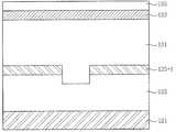
종래 금속 배선을 형성하기 위한 이중 다마신 방법의 일부를 도 1a 내지 도 1d를 이용하여 설명한다.A part of the dual damascene method for forming a conventional metal wiring will be described using Figs. 1A to 1D.
도 1a를 참조하면, 피식각층(1) 상부에 다공성 저유전막(3)을 형성한 다음, 하드마스크막(5)을 형성한다.Referring to FIG. 1A, a porous low
도 1a의 하드마스크막 상부에 포토레지스트층(미도시)을 형성한 다음, 리소그래피(lithography) 공정을 수행하여 도 1b에 도시한 바와 같이 포토레지스트 패턴(7)을 형성한다.A photoresist layer (not shown) is formed on the hard mask layer of FIG. 1A, and then a lithography process is performed to form the photoresist pattern 7 as shown in FIG. 1B.
상기 도 1b의 포토레지스트 패턴(7)을 식각 마스크로 하드마스크막(3)에 대 한 식각 공정을 수행하여 도 1c에 도시한 바와 같이 하드마스크 패턴(5-1)을 형성한다.An etching process is performed on the
상기 도 1c의 결과물에 대한 애싱 공정을 수행하여 포토레지스트 패턴(7)을 제거한 다음, 남아있는 하드마스크막 패턴(5-1)을 식각 마스크로 하부 다공성 저유전막(3)에 대한 식각 공정을 수행하여 도 1d에 도시한 바와 같은 비아 콘택홀(8)을 형성한다.The ashing process is performed on the resultant of FIG. 1C to remove the photoresist pattern 7, and then the etching process is performed on the lower porous low-k
이 후, 상기 형성된 비아 콘택홀에 대한 후속 공정으로 트렌치(미도시)를 형성하는 SA 이중 다마신 공정을 수행한 후, 금속층(미도시)을 매립하여 금속 배선(미도시)을 형성한다.Thereafter, after the SA double damascene process of forming a trench (not shown) as a subsequent process for the formed via contact hole, a metal layer (not shown) is embedded to form a metal wiring (not shown).
현재, 소자의 선폭이 90nm 이하로 줄어들면서 상기 다공성 저유전막(3)으로 유전상수 값이 2.7 이하인 물질을 사용하며, 기존 다공성 저유전막 내에 포함되어 있는 카본(carbon)의 도핑(doping)양을 조절하거나, 물질 내의 다공성(porosity)을 증가시켜 보다 낮은 저유전상수(k=~2.3 이하) 값을 얻고자 하였다.At present, as the line width of the device is reduced to 90 nm or less, a material having a dielectric constant value of 2.7 or less is used as the porous low
하지만, 상기 다공성 저유전막은 도핑된 카본 함량이나, 다공성 정도가 증가하면서, 큰 비표면적을 가져 산소에 의해 쉽게 열화된다. 즉, 상기 비아 콘택홀을 형성하는 식각 공정 전 또는 후나, 후속 공정인 트렌치를 형성하기 위한 식각 공정 전 또는 후에, 사용된 포토레지스트 패턴 및 식각 마스크 패턴들을 제거하기 위한 O2 애싱 공정 수행하는데, 이때 노출되어 있던 다공성 저유전막의 주요 성분인 카본이 상기 산소와 반응하면서 중합체를 형성하여 저유전막 내의 탄소가 고갈 (depletion)되거나, CO2 가스로 날아가면서 기공이 증가하여 유전 상수값이 증가된다. 이에 따라, 저유전막질이 저하(degradation)되어 금속 배선이 누설(leakage) 되는 등 소자의 특성이 열화되어 배선의 신뢰도(reliability)가 감소된다.However, the porous low-dielectric film has a large specific surface area and is easily deteriorated by oxygen as the doped carbon content or porosity increases. That is, before or after the etching process for forming the via contact hole, or before or after the etching process for forming a trench which is a subsequent process, an O2 ashing process for removing the used photoresist pattern and etching mask patterns is performed. Carbon, which is a major component of the exposed porous low dielectric film, reacts with the oxygen to form a polymer, thereby depleting carbon in the low dielectric film, or increasing porosity as it flies to CO2 gas, thereby increasing the dielectric constant value. As a result, the characteristics of the device deteriorate, such as degradation of the low dielectric film quality and leakage of the metal wiring, thereby reducing the reliability of the wiring.
이를 개선하기 위하여, 상기 애싱 가스를 산소 가스 대신 수소(H2)나 질소(NH3) 등을 사용함으로써 애싱의 손실(damage)을 최소화시켜 유전상수의 증가를 억제하려 하였으나, 이 또한 낮은 애싱 비(rate)와 잔유물(residue)이 발생하는 단점이 있다.In order to improve this, the ashing gas is used instead of oxygen gas to suppress the increase of dielectric constant by minimizing ashing loss by using hydrogen (H2 ) or nitrogen (NH3 ), but this also lower ashing ratio. (rate) and residues (residue) has the disadvantage that occurs.
이에 본 발명자들은 활발한 연구 결과 고가의 장비 개발 없이도 상기한 종래의 문제점을 개선할 수 있는 새로운 이중 다마신 방법을 개발하여 본 발명을 완성하였다.Accordingly, the present inventors have completed the present invention by developing a new dual damascene method that can improve the above-mentioned conventional problems without developing expensive equipment.
본 발명은 비아 및 트렌치로 이루어지는 이중 다마신 패턴 형성 공정에서 이중 하드마스크를 사용하여 비아홀 및 트렌치를 형성함으로써, 후속 애싱 공정 시에 저유전 층간 절연막의 유전 상수값이 상승하는 것을 방지할 수 있는 이중 다마신 패턴 형성 방법을 제공하는 것에 그 목적이 있다.According to the present invention, a via hole and a trench are formed using a double hard mask in a double damascene pattern formation process consisting of vias and trenches, thereby preventing the dielectric constant value of the low dielectric interlayer insulating film from rising during the subsequent ashing process. An object thereof is to provide a method for forming a damascene pattern.
상기 목적을 달성하기 위하여 본 발명에서는In the present invention to achieve the above object
(a) 피식각층 상부에 비아홀용 다공성 저유전막을 형성하는 단계;(a) forming a porous low dielectric film for via holes on the etched layer;
(b) 상기 다공성 저유전막 상부에 제 1 하드마스크막 및 제 2 하드마스크막 의 이중 하드마스크막을 순차적으로 형성하는 단계(b) sequentially forming a double hard mask layer of a first hard mask layer and a second hard mask layer on the porous low dielectric layer;
(c) 상기 제 2 하드마스크막 상부에 리소그래피 공정에 의한 제 1 포토레지스트 패턴을 형성하는 단계;(c) forming a first photoresist pattern on the second hard mask layer by a lithography process;
(d) 상기 제 1 포토레지스트 패턴을 식각 마스크로 상기 제 1 하드마스크막이 노출될 때까지 상기 제 2 하드마스크막에 대한 식각 공정을 수행하여 제 2 하드마스크막 패턴을 형성하는 단계;(d) forming a second hard mask layer pattern by performing an etching process on the second hard mask layer until the first hard mask layer is exposed using the first photoresist pattern as an etching mask;
(e) 상기 결과물에 대한 애싱 공정으로 상기 제 1 포토레지스트 패턴을 제거하여 제 2 하드마스크막 패턴을 노출시키는 단계;(e) exposing the second hardmask film pattern by removing the first photoresist pattern by an ashing process on the resultant product;
(f) 상기 제 2 하드마스크막 패턴을 식각 마스크로 상기 제 1 하드마스크막과 상기 비아홀용 다공성 저유전막에 대한 부분 식각 공정을 수행하여 금속배선용 비아홀을 형성하는 단계;(f) forming a via hole for metal wiring by performing a partial etching process on the first hard mask layer and the porous low dielectric layer for the via hole using the second hard mask layer pattern as an etching mask;
(g) 상기 금속배선용 비아홀을 포함하는 제 1 하드마스크막 상부에 트렌치용 다공성 저유전막을 형성하는 단계;(g) forming a porous low dielectric film for trenches on the first hard mask film including the via hole for metal wiring;
(h) 상기 트렌치용 다공성 저유전막 상부에 제 3 하드마스크막 및 제 4 하드마스크막의 이중 하드마스크막을 순차적으로 형성하는 단계;(h) sequentially forming a double hard mask layer of a third hard mask layer and a fourth hard mask layer on the porous low-k dielectric layer;
(i) 상기 제 4 하드마스크막 상부에 리소그래피 공정에 의한 제 2 포토레지스트 패턴을 형성하는 단계;(i) forming a second photoresist pattern on the fourth hard mask layer by a lithography process;
(j) 상기 제 2 포토레지스트 패턴을 식각 마스크로 상기 제 3 하드마스크막이 노출될 때까지 상기 제 4 하드마스크막에 대한 식각공정을 수행하여 제 4 하드마스크막 패턴을 형성하는 단계;(j) forming a fourth hard mask layer pattern by performing an etching process on the fourth hard mask layer until the third hard mask layer is exposed using the second photoresist pattern as an etching mask;
(k) 상기 결과물에 대한 애싱 공정으로 제 2 포토레지스트 패턴을 제거하여 상기 제 4 하드마스크막 패턴을 노출시키는 단계;(k) exposing the fourth hard mask layer pattern by removing a second photoresist pattern through an ashing process on the resultant;
(l) 상기 제 4 하드마스크막 패턴을 식각 마스크로 상기 피식각층이 노출될 때까지 상기 제 3 하드마스크막, 상기 트렌치용 다공성 저유전막 및 금속배선용 비아홀에 대한 부분 식각 공정을 수행하여 금속배선용 트렌치를 형성하는 단계; 및(l) a trench for metal wiring by performing a partial etching process on the third hard mask film, the porous low dielectric film for trenches and via holes for metal wiring until the etched layer is exposed using the fourth hard mask film pattern as an etching mask; Forming a; And
(m) 상기 금속배선용 트렌치를 포함하는 전면에 평탄화된 구리 배선을 매립하는 단계를 포함하는 이중 다마신 패턴 형성 방법을 제공한다.(m) a method of forming a dual damascene pattern, comprising the step of embedding the planarized copper wiring on the entire surface including the trench for metal wiring.
이하, 본 발명을 도면을 들어 상세히 설명한다.Hereinafter, the present invention will be described in detail with reference to the drawings.
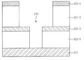
도 2a를 참조하면, 피식각층(121) 상부에 비아홀용 다공성 저유전막(123)을 형성한 다음, 제 1 하드마스크막(125) 및 제 2 하드마스크막(127)의 이중 하드마스크막을 순차적으로 형성한다.Referring to FIG. 2A, after forming the porous low
이때, 상기 다공성 저유전막은 SOG(spin on glass) 방법으로 SiOC계 물질을 3000~5000Å 두께로 형성한다.In this case, the porous low-k dielectric layer forms a SiOC-based material in a thickness of 3000 to 5000 kPa by a spin on glass (SOG) method.
상기 제 1 하드마스크막은 화학기상증착법(chemical vapor deposition; 이하 "CVD"라 칭함)으로 실리카 카바이드(SiC) 또는 실리카 나이트라이드(SiN)를 100~1000Å두께로 형성한다.The first hard mask film is formed of silica carbide (SiC) or silica nitride (SiN) with a thickness of 100 to 1000 Pa by chemical vapor deposition (hereinafter referred to as "CVD").
상기 제 2 하드마스크막은 상기 제 1 하드마스크막보다 식각이 쉽게 되는 물질인 실리카(SiO2), LP-TEOS(low pressure-tetraethoxysilicate glass), PE-TEOS(plasma enhanced-tetraethoxysilicate glass), FSG (fluorosilicate glass) 또는 PE-SiH4(plasma enhanced-silane)를 CVD 방법을 사용하여 100~1000Å 두께로 형성한다.The second hard mask layer may include silica (SiO2 ), low pressure-tetraethoxysilicate glass (LP-TEOS), plasma enhanced-tetraethoxysilicate glass (PE-TEOS), and fluorosilicate, which are easier to etch than the first hard mask layer. glass) or PE-SiH4 (plasma enhanced-silane) is formed to a thickness of 100 ~ 1000Å by CVD method.
도 2a의 제 2 하드마스크막(127) 상부에 포토레지스트층(미도시)을 형성한 다음, 포토/에치 공정을 수행하여 도 2b에 도시한 바와 같이 제 1 포토레지스트 패턴(129)을 형성한다.After forming a photoresist layer (not shown) on the second
상기 도 2b의 제 1 포토레지스트 패턴(129)을 식각 마스크로, 상기 제 1 하드마스크막(125)이 노출될 때까지 상기 제 2 하드마스크막(127)에 대한 식각 공정을 수행하여 도 2c에 도시한 바와 같이 제 2 하드마스크막 패턴(127-1)을 형성한다.Using the
이때, 상기 식각 공정은 CF4, C4F8, C2F6 또는 CHF3 등의 가스를 이용하는 플라즈마 건식각 방법으로 수행된다.In this case, the etching process is performed by a plasma dry etching method using a gas such as CF4 , C4 F8 , C2 F6 or CHF3 .
그 다음, 상기 도 2c의 제 2 하드마스크막 패턴(127) 상부에 잔류하는 제 1 포토레지스트 패턴에 대한 애싱 공정을 수행하여 도 2d에 도시한 바와 같이 상기 제 1 포토레지스트 패턴(129)을 제거한다.Next, an ashing process is performed on the first photoresist pattern remaining on the second hard
상기 애싱 공정은 O2, H2 및 NH3 가스를 이용하여, RIE 애싱이나 RF 파워가 적용된 방법으로 수행된다.The ashing process is performed by using RIE ashing or RF power using O2 , H2 and NH3 gas.
이때, 상기 비아홀용 다공성 저유전막(123) 상부에는 제 1 하드마스크막이 형성되어 있으므로, 애싱 공정 시에 상기 다공성 저유전막이 손상되지 않도록 방지한다.At this time, since the first hard mask film is formed on the via hole porous low
상기 도 2d의 애싱 공정 후에 노출된 상기 제 2 하드마스크막 패턴(127-1)을 식각 마스크로 상기 제 1 하드마스크막(125)과 상기 비아홀용 다공성 저유전막(123)에 대한 부분 식각 공정을 수행하여 도 2e에 도시한 바와 같이 금속배선용 비아홀(130)을 형성한다.A partial etching process is performed on the first
이때, 상기 식각 공정은 상기 방법과 동일한 플라즈마 건식각 방법으로 실시하되, 식각 시 비아홀용 다공성 저유전막(123)이 부분적으로만 식각되도록 실시한다.In this case, the etching process may be performed by the same plasma dry etching method as the above method, in which the porous low-
그리고, 상기 도 2e의 금속배선용 비아홀(130)을 포함하는 제 1 하드마스크막 상부에 도 2f에 도시한 바와 같이 트렌치용 다공성 저유전막(131), 제 3 하드마스크막(133) 및 제 4 하드마스크막(135)의 이중 하드마스크막을 순차적으로 형성한다.In addition, as illustrated in FIG. 2F, the porous low
이때, 상기 다공성 저유전막은 비아홀용 다공성 저유전막 형성 방법과 동일한 방법에 의해 2000~5000Å 두께로 형성된다.In this case, the porous low dielectric film is formed to a thickness of 2000 ~ 5000Å by the same method as the porous low dielectric film forming method for via holes.
상기 제 3 하드마스크막은 SiC 또는 SiN를 CVD 방법을 사용하여 100~1000Å 두께로 형성하고, 상기 제 4 하드마스크막은 상기 제 3 하드마스크막보다 쉽게 식각되는 물질인 SiO2, LP-TEOS, PE-TEOS, FSG 또는 PE-SiH4를 CVD 방법을 사용하여 100~1000Å 두께로 형성한다.The third hard mask layer is formed of SiC or SiN to a thickness of 100 ~ 1000Å by using a CVD method, the fourth hard mask layer is SiO2 , LP-TEOS, PE- is a material that is more easily etched than the third hard mask layer TEOS, FSG or PE-SiH4 is formed to a thickness of 100 to 1000 mm by CVD.
상기 도 2f의 제 4 하드마스크막(135) 상부에 포토레지스트층(미도시)을 형성한 다음, 포토/에치 공정을 수행하여 도 2g에 도시한 바와 같이 제 2 포토레지스 트 패턴(137)을 형성한다.A photoresist layer (not shown) is formed on the fourth
상기 도 2g의 제 2 포토레지스트 패턴(137)을 식각 마스크로, 상기 제 3 하드마스크막(133)이 노출될 때까지 상기 제 4 하드마스크막(135)에 대한 식각 공정을 수행하여 도 2h에 도시한 바와 같이 제 4 하드마스크막 패턴(135-1)을 형성한다.Using the
이때, 상기 식각 공정은 비아홀 형성을 위한 하드마스크 패턴 방법과 동일한 방법으로 수행된다.In this case, the etching process is performed in the same manner as the hard mask pattern method for forming via holes.
상기 도 2h의 제 4 하드마스크막 패턴(135-1) 상부에 잔류하는 제 2 포토레지스트 패턴(137)에 대한 애싱 공정을 수행하여 도 2i에 도시한 바와 같이 상기 제 2 포토레지스트 패턴(127)을 제거한다.The
상기 애싱 공정은 O2, H2 및 NH3 가스를 이용하여, RIE 애싱이나 F 파워가 적용된 방법으로 수행된다.The ashing process is performed by using RIE ashing or F power using O2 , H2 and NH3 gas.
이때, 상기 트렌치용 다공성 저유전막(131) 상부에는 제 3 하드마스크막이 형성되어 있으므로, 애싱 공정 시에 상기 트렌치용 다공성 저유전막이 손상되지 않도록 방지한다.In this case, since a third hard mask film is formed on the trench porous low
상기 도 2i의 제 4 하드마스크막 패턴(135-1)을 식각 마스크로 상기 피식각층(121)이 노출될 때까지 상기 제 3 하드마스크막(133), 상기 트렌치용 다공성 저유전막(131) 및 금속배선용 비아홀(130)에 대한 부분 식각 공정을 수행하여 도 2j에 도시한 바와 같이 금속배선용 트렌치(139)를 형성한다.The third
이때, 상기 식각 공정은 플라즈마 건식각 방법을 이용하여 CF4, C4F8, C2F6또는 CHF3 등의 가스를 사용하여 수행된다.In this case, the etching process is performed using a gas such as CF4 , C4 F8 , C2 F6 or CHF3 using a plasma dry etching method.
또한, 상기 공정 시에 SA 이중 다마신 공정을 적용함으로써, 트렌치 식각 시 적용되던 유기반사방지막(BARC) 코팅 공정 및 상기 BARC의 식각 공정 등을 사용하지 않으므로, 공정 단계가 축소된다.In addition, by applying the SA double damascene process in the process, since the organic anti-reflective coating (BARC) coating process and the BARC etching process applied during the trench etching is not used, the process step is reduced.
도 2k를 참조하면, 상기 도 2j에서 형성된 상기 금속배선용 트렌치(139)를 포함하는 전면에 구리층(141)을 매립한 다음, 상기 트렌치용 다공성 저유전막(131)을 연마 정지막으로 하는 평탄화공정을 수행하여 도 2l에 도시한 바와 같이 제 3 하드마스크막(133)이 제거된 구리 배선(143)을 형성한다.Referring to FIG. 2K, a
상기 구리층은 스퍼터링이나 CVD 또는 전기도금법으로 수행되는데, 상기 전기 도금법으로 형성되는 경우, 씨드 금속막(미도시)을 먼저 배리어 메탈층 상에 형성한 후 매립하는 것이 바람직하다.The copper layer is performed by sputtering, CVD, or electroplating. In the case of forming the electroplating method, a seed metal film (not shown) is preferably formed on the barrier metal layer and then embedded.
전술한 바와 같이 본 발명에서는 다공성 저유전막을 이용한 금속 배선 형성 공정 시에, 각각의 다공성 저유전막에 상부에 이중 하드마스크막을 형성함으로써, 일반적인 애싱 공정에 의해 상기 다공성 저유전막이 손상되는 것을 방지하여 유전상수가 증가하는 것을 방지할 수 있다.As described above, in the present invention, in the metal wiring forming process using the porous low dielectric film, a double hard mask film is formed on each porous low dielectric film, thereby preventing the porous low dielectric film from being damaged by a general ashing process. The constant can be prevented from increasing.
또한, 상기 금속 배선 형성 공정 시에 SA 이중 다마신 공정을 적용함으로써, 트렌치 식각 시 적용되었던 BARC 코팅 및 식각 공정을 삭제할 수 있으므로, 공정 단계의 축소를 가져온다.In addition, by applying the SA double damascene process in the metal wiring forming process, it is possible to delete the BARC coating and etching process applied during the trench etching, resulting in a reduction of the process step.
이상에서 살펴본 바와 같이, 본 발명은 다공성 저유전막을 이용한 금속 배선 형성 공정 시에, 각각의 다공성 저유전막에 상부에 이중 하드마스크막을 형성함으로써, 후속 애싱 공정에 의한 상기 다공성 저유전막의 손상을 막아 유전상수의 증가를 방지할 수 있다.As described above, the present invention forms a double hard mask on top of each porous low dielectric layer during the metal wiring formation process using the porous low dielectric layer, thereby preventing damage to the porous low dielectric layer by a subsequent ashing process. The increase of the constant can be prevented.
또한, 상기 금속 배선 형성 공정 시에 SA 이중 다마신 공정을 적용함으로써, 트렌치 식각 시 적용되었던 BARC 코팅 및 식각 공정을 삭제하여, 공정 단계의 축소를 가져온다.In addition, by applying the SA double damascene process in the metal wiring forming process, it eliminates the BARC coating and etching process applied during the trench etching, resulting in a reduction of the process step.
Claims (20)
Translated fromKoreanPriority Applications (1)
| Application Number | Priority Date | Filing Date | Title |
|---|---|---|---|
| KR1020040115260AKR101138075B1 (en) | 2004-12-29 | 2004-12-29 | Method for Forming Dual Damascene Pattern |
Applications Claiming Priority (1)
| Application Number | Priority Date | Filing Date | Title |
|---|---|---|---|
| KR1020040115260AKR101138075B1 (en) | 2004-12-29 | 2004-12-29 | Method for Forming Dual Damascene Pattern |
Publications (2)
| Publication Number | Publication Date |
|---|---|
| KR20060075890A KR20060075890A (en) | 2006-07-04 |
| KR101138075B1true KR101138075B1 (en) | 2012-04-24 |
Family
ID=37168381
Family Applications (1)
| Application Number | Title | Priority Date | Filing Date |
|---|---|---|---|
| KR1020040115260AExpired - Fee RelatedKR101138075B1 (en) | 2004-12-29 | 2004-12-29 | Method for Forming Dual Damascene Pattern |
Country Status (1)
| Country | Link |
|---|---|
| KR (1) | KR101138075B1 (en) |
Cited By (1)
| Publication number | Priority date | Publication date | Assignee | Title |
|---|---|---|---|---|
| US10790186B2 (en) | 2017-10-20 | 2020-09-29 | Samsung Electronics Co., Ltd. | Semiconductor device including a passivation spacer and method of fabricating the same |
Families Citing this family (2)
| Publication number | Priority date | Publication date | Assignee | Title |
|---|---|---|---|---|
| KR100685137B1 (en)* | 2005-10-05 | 2007-02-22 | 동부일렉트로닉스 주식회사 | Method of forming copper metal wiring and semiconductor device comprising copper metal wiring formed thereby |
| KR100842670B1 (en)* | 2006-12-15 | 2008-06-30 | 동부일렉트로닉스 주식회사 | Semiconductor device manufacturing method |
Citations (2)
| Publication number | Priority date | Publication date | Assignee | Title |
|---|---|---|---|---|
| US20030054656A1 (en)* | 2001-09-19 | 2003-03-20 | Nec Corporation | Method for manufacturing semiconductor device including two-step ashing process of N2 plasma gas and N2/H2 plasma gas |
| KR100391992B1 (en)* | 2000-12-08 | 2003-07-22 | 삼성전자주식회사 | METHOD OF FORMING SEMICONDUCTOR DEVICES HAVING SiOC LAYER |
- 2004
- 2004-12-29KRKR1020040115260Apatent/KR101138075B1/ennot_activeExpired - Fee Related
Patent Citations (2)
| Publication number | Priority date | Publication date | Assignee | Title |
|---|---|---|---|---|
| KR100391992B1 (en)* | 2000-12-08 | 2003-07-22 | 삼성전자주식회사 | METHOD OF FORMING SEMICONDUCTOR DEVICES HAVING SiOC LAYER |
| US20030054656A1 (en)* | 2001-09-19 | 2003-03-20 | Nec Corporation | Method for manufacturing semiconductor device including two-step ashing process of N2 plasma gas and N2/H2 plasma gas |
Cited By (2)
| Publication number | Priority date | Publication date | Assignee | Title |
|---|---|---|---|---|
| US10790186B2 (en) | 2017-10-20 | 2020-09-29 | Samsung Electronics Co., Ltd. | Semiconductor device including a passivation spacer and method of fabricating the same |
| US11251070B2 (en) | 2017-10-20 | 2022-02-15 | Samsung Electronics Co., Ltd. | Semiconductor device including a passivation spacer and method of fabricating the same |
Also Published As
| Publication number | Publication date |
|---|---|
| KR20060075890A (en) | 2006-07-04 |
Similar Documents
| Publication | Publication Date | Title |
|---|---|---|
| US7828987B2 (en) | Organic BARC etch process capable of use in the formation of low K dual damascene integrated circuits | |
| US7157366B2 (en) | Method of forming metal interconnection layer of semiconductor device | |
| US7871923B2 (en) | Self-aligned air-gap in interconnect structures | |
| US6358842B1 (en) | Method to form damascene interconnects with sidewall passivation to protect organic dielectrics | |
| US6372636B1 (en) | Composite silicon-metal nitride barrier to prevent formation of metal fluorides in copper damascene | |
| KR100430472B1 (en) | Method for forming wiring using dual damacine process | |
| US7470616B1 (en) | Damascene wiring fabrication methods incorporating dielectric cap etch process with hard mask retention | |
| US20050079706A1 (en) | Dual damascene structure and method | |
| US7015133B2 (en) | Dual damascene structure formed of low-k dielectric materials | |
| US7622808B2 (en) | Semiconductor device and having trench interconnection | |
| KR100532446B1 (en) | Method for forming metal interconnection layer of semiconductor device | |
| US7572733B2 (en) | Gas switching during an etch process to modulate the characteristics of the etch | |
| KR101138075B1 (en) | Method for Forming Dual Damascene Pattern | |
| US6465340B1 (en) | Via filled dual damascene structure with middle stop layer and method for making the same | |
| US6465343B1 (en) | Method for forming backend interconnect with copper etching and ultra low-k dielectric materials | |
| EP1235263A2 (en) | Gas switching during an etch process to modulate the characteristics of the etch | |
| KR100909175B1 (en) | How to form a dual damascene pattern | |
| US6365505B1 (en) | Method of making a slot via filled dual damascene structure with middle stop layer | |
| KR100440080B1 (en) | Method for forming metal line of semiconductor device | |
| KR101024871B1 (en) | How to form a dual damascene pattern | |
| JP2005328060A (en) | Manufacturing method of semiconductor device | |
| KR100439111B1 (en) | Method for forming metal line in semiconductor device | |
| JP3774399B2 (en) | Dual damascene structure and method for forming the same, and semiconductor device and method for manufacturing the same | |
| KR20060075887A (en) | Metal wiring formation method of semiconductor device | |
| KR100483838B1 (en) | Dual damascene process of metal wire |
Legal Events
| Date | Code | Title | Description |
|---|---|---|---|
| PA0109 | Patent application | St.27 status event code:A-0-1-A10-A12-nap-PA0109 | |
| PN2301 | Change of applicant | St.27 status event code:A-3-3-R10-R13-asn-PN2301 St.27 status event code:A-3-3-R10-R11-asn-PN2301 | |
| R17-X000 | Change to representative recorded | St.27 status event code:A-3-3-R10-R17-oth-X000 | |
| PG1501 | Laying open of application | St.27 status event code:A-1-1-Q10-Q12-nap-PG1501 | |
| A201 | Request for examination | ||
| P11-X000 | Amendment of application requested | St.27 status event code:A-2-2-P10-P11-nap-X000 | |
| P13-X000 | Application amended | St.27 status event code:A-2-2-P10-P13-nap-X000 | |
| PA0201 | Request for examination | St.27 status event code:A-1-2-D10-D11-exm-PA0201 | |
| R17-X000 | Change to representative recorded | St.27 status event code:A-3-3-R10-R17-oth-X000 | |
| D13-X000 | Search requested | St.27 status event code:A-1-2-D10-D13-srh-X000 | |
| D14-X000 | Search report completed | St.27 status event code:A-1-2-D10-D14-srh-X000 | |
| E902 | Notification of reason for refusal | ||
| PE0902 | Notice of grounds for rejection | St.27 status event code:A-1-2-D10-D21-exm-PE0902 | |
| T11-X000 | Administrative time limit extension requested | St.27 status event code:U-3-3-T10-T11-oth-X000 | |
| T11-X000 | Administrative time limit extension requested | St.27 status event code:U-3-3-T10-T11-oth-X000 | |
| T11-X000 | Administrative time limit extension requested | St.27 status event code:U-3-3-T10-T11-oth-X000 | |
| E13-X000 | Pre-grant limitation requested | St.27 status event code:A-2-3-E10-E13-lim-X000 | |
| P11-X000 | Amendment of application requested | St.27 status event code:A-2-2-P10-P11-nap-X000 | |
| P13-X000 | Application amended | St.27 status event code:A-2-2-P10-P13-nap-X000 | |
| E701 | Decision to grant or registration of patent right | ||
| PE0701 | Decision of registration | St.27 status event code:A-1-2-D10-D22-exm-PE0701 | |
| GRNT | Written decision to grant | ||
| PR0701 | Registration of establishment | St.27 status event code:A-2-4-F10-F11-exm-PR0701 | |
| PR1002 | Payment of registration fee | St.27 status event code:A-2-2-U10-U11-oth-PR1002 Fee payment year number:1 | |
| PG1601 | Publication of registration | St.27 status event code:A-4-4-Q10-Q13-nap-PG1601 | |
| LAPS | Lapse due to unpaid annual fee | ||
| PC1903 | Unpaid annual fee | St.27 status event code:A-4-4-U10-U13-oth-PC1903 Not in force date:20150413 Payment event data comment text:Termination Category : DEFAULT_OF_REGISTRATION_FEE | |
| PC1903 | Unpaid annual fee | St.27 status event code:N-4-6-H10-H13-oth-PC1903 Ip right cessation event data comment text:Termination Category : DEFAULT_OF_REGISTRATION_FEE Not in force date:20150413 | |
| P22-X000 | Classification modified | St.27 status event code:A-4-4-P10-P22-nap-X000 | |
| R18-X000 | Changes to party contact information recorded | St.27 status event code:A-5-5-R10-R18-oth-X000 | |
| PN2301 | Change of applicant | St.27 status event code:A-5-5-R10-R13-asn-PN2301 St.27 status event code:A-5-5-R10-R11-asn-PN2301 |