KR101138041B1 - Optical system calibration method of in-line substrate inspection apparatus and inspection apparatus of in-line substrate - Google Patents
Optical system calibration method of in-line substrate inspection apparatus and inspection apparatus of in-line substrateDownload PDFInfo
- Publication number
- KR101138041B1 KR101138041B1KR1020100074553AKR20100074553AKR101138041B1KR 101138041 B1KR101138041 B1KR 101138041B1KR 1020100074553 AKR1020100074553 AKR 1020100074553AKR 20100074553 AKR20100074553 AKR 20100074553AKR 101138041 B1KR101138041 B1KR 101138041B1
- Authority
- KR
- South Korea
- Prior art keywords
- substrate
- optical system
- inspection
- calibration
- light
- Prior art date
- Legal status (The legal status is an assumption and is not a legal conclusion. Google has not performed a legal analysis and makes no representation as to the accuracy of the status listed.)
- Expired - Fee Related
Links
Images


Classifications
- G—PHYSICS
- G01—MEASURING; TESTING
- G01N—INVESTIGATING OR ANALYSING MATERIALS BY DETERMINING THEIR CHEMICAL OR PHYSICAL PROPERTIES
- G01N21/00—Investigating or analysing materials by the use of optical means, i.e. using sub-millimetre waves, infrared, visible or ultraviolet light
- G01N21/84—Systems specially adapted for particular applications
- G01N21/88—Investigating the presence of flaws or contamination
- G01N21/93—Detection standards; Calibrating baseline adjustment, drift correction
- G—PHYSICS
- G01—MEASURING; TESTING
- G01N—INVESTIGATING OR ANALYSING MATERIALS BY DETERMINING THEIR CHEMICAL OR PHYSICAL PROPERTIES
- G01N21/00—Investigating or analysing materials by the use of optical means, i.e. using sub-millimetre waves, infrared, visible or ultraviolet light
- G01N21/84—Systems specially adapted for particular applications
- G01N21/88—Investigating the presence of flaws or contamination
- G01N21/89—Investigating the presence of flaws or contamination in moving material, e.g. running paper or textiles
- G01N21/892—Investigating the presence of flaws or contamination in moving material, e.g. running paper or textiles characterised by the flaw, defect or object feature examined
- G01N21/896—Optical defects in or on transparent materials, e.g. distortion, surface flaws in conveyed flat sheet or rod
- G—PHYSICS
- G01—MEASURING; TESTING
- G01N—INVESTIGATING OR ANALYSING MATERIALS BY DETERMINING THEIR CHEMICAL OR PHYSICAL PROPERTIES
- G01N21/00—Investigating or analysing materials by the use of optical means, i.e. using sub-millimetre waves, infrared, visible or ultraviolet light
- G01N21/84—Systems specially adapted for particular applications
- G01N21/88—Investigating the presence of flaws or contamination
- G01N21/93—Detection standards; Calibrating baseline adjustment, drift correction
- G01N2021/933—Adjusting baseline or gain (also for web inspection)
Landscapes
- Analytical Chemistry (AREA)
- Immunology (AREA)
- Physics & Mathematics (AREA)
- Health & Medical Sciences (AREA)
- Life Sciences & Earth Sciences (AREA)
- Chemical & Material Sciences (AREA)
- General Health & Medical Sciences (AREA)
- Biochemistry (AREA)
- Pathology (AREA)
- General Physics & Mathematics (AREA)
- Engineering & Computer Science (AREA)
- Textile Engineering (AREA)
- Investigating Materials By The Use Of Optical Means Adapted For Particular Applications (AREA)
- Liquid Crystal (AREA)
Abstract
Translated fromKoreanDescription
Translated fromKorean본 발명은, 표시용 패널 등의 제조에 이용되는 유리 기판 및 플라스틱 기판 등의 결함을 레이저 광을 이용하여 검출하는 인라인 기판 검사 장치의 광학 시스템 교정 방법 및 인라인 기판 검사 장치에 관한 것으로, 특히 유리 기판이나 플라스틱 기판 등의 제조 라인 내나, 이들을 이용한 표시용 패널 기판의 제조 라인 내에 갖추어진 검사 장치의 광학 시스템 보수 작업에 적합한 인라인 기판 검사 장치의 광학 시스템 교정 방법 및 인라인 기판 검사 장치에 관한 것이다.The present invention relates to an optical system calibrating method and an in-line substrate inspecting apparatus for an in-line substrate inspecting apparatus for detecting defects such as glass substrates and plastic substrates used for manufacturing display panels and the like using laser light, And more particularly to an optical system correcting method and an in-line substrate inspecting apparatus for an in-line substrate inspecting apparatus suitable for an optical system maintenance operation of an inspecting apparatus provided in a manufacturing line of a display panel substrate using the same.
표시용 패널로서 이용되는 액정 디스플레이 장치의 TFT(Thin Film Transistor)기판이나 컬러 필터 기판, 플라즈마 디스플레이 패널용 기판, 유기EL(Electroluminescence) 표시 패널용 기판 등의 제조는, 포토리소그래피 기술에 의해, 유리 기판이나 플라스틱 기판 등의 기판 상에 패턴을 형성해서 실시된다. 그 때, 기판에 상처나 이물질 등의 결함이 존재하면, 패턴이 양호하게 형성되지 않고, 불량의 원인이 된다. 이 때문에, 기판 검사 장치를 이용하여, 기판의 상처나 이물질 등의 결함 검사가 실시된다.(Thin Film Transistor) substrate, a color filter substrate, a plasma display panel substrate, and an organic EL (Electroluminescence) display panel substrate of a liquid crystal display device used as a display panel can be manufactured by photolithography, Or a plastic substrate or the like. At this time, if defects such as scratches or foreign substances are present on the substrate, the pattern is not formed well and causes defects. Therefore, defects such as scratches and foreign substances on the substrate are inspected using the substrate inspection apparatus.
기판 검사 장치는, 레이저 광 등의 검사광을 기판으로 조사하여, 기판으로부터의 반사광 또는 산란광을 수광하여, 기판의 상처나 이물질 등의 결함을 검출하는 것이다. 검사광에 의해 기판이 주사되기 때문에, 기판 전체의 검사에는 시간이 걸린다. 그 때문에, 종래는, 유리 기판이나 플라스틱 기판 등의 제조 라인 내나, 이들을 채용한 표시용 패널 기판의 제조 라인 내에서, 기판의 결함을 실시간으로 검사하고 있다. 이렇게 제조 라인 내에서, 실시간으로 검사를 실시하는 기판 검사 장치에 있어서는, 광학 시스템의 정기적인 레이저 파워의 관리, 검출 감도의 조정 작업 등의 교정 작업은 필요 불가결하게 되어 있다. 종래에는 기판 검사 장치의 광학 시스템의 교정 작업은, 검사 스테이지 상에 표준입자를 도포한 기준 샘플 기판을 탑재함으로써 광학 시스템의 교정 작업을 실시했었다. 이와 같은 교정 작업에 있어서는, 광학 시스템의 교정 작업 실시를 위해서, 표준 입자 부착 기판을 검사 스테이지 상으로 작업자가 사람 손으로 실어서 실시할 필요가 있었다. 이처럼 기준 샘플 기판을 탑재해서 교정을 실시하는 것으로, 특허문헌 1에 기재된 것과 같은 것이 알려져 있다.A substrate inspection apparatus irradiates inspection light such as a laser beam onto a substrate to receive reflected light or scattered light from the substrate to detect defects such as scratches and foreign substances on the substrate. Since the substrate is scanned by the inspection light, it takes time to inspect the entire substrate. Therefore, conventionally, defects of a substrate are inspected in real time in a production line of a glass substrate, a plastic substrate, or the like, or in a production line of a display panel substrate employing them. In such a substrate inspecting apparatus that conducts inspections in real time in a manufacturing line, it is indispensable to calibrate, for example, the periodic laser power control of the optical system and the adjustment of the detection sensitivity. Conventionally, a calibration operation of an optical system of a substrate inspection apparatus has been performed by mounting a reference sample substrate coated with standard particles on an inspection stage. In such a calibration work, it is necessary to carry out the calibration work of the optical system by placing the standard particle-adhered substrate on the inspection stage with the operator's hand. It is known that the reference sample substrate is mounted and calibrated as described in
[특허문헌 1] 특개2003-059994호 공보[Patent Document 1] JP-A-2003-059994
특허문헌 1에 기재된 것은, 반도체의 웨이퍼를 검사하는 장치의 관리 방법에 관계되는 기술이며, 복수의 피검사 샘플을 연속해서 측정하는 검사 도중, 미리 세트된 표준 샘플 전용 카세트로부터 자동적으로 표준 샘플을 공급하여 측정을 실시하고, 상기 표준 샘플의 측정 결과와 교정 기준?관리 기준과의 대조를 실시하여 검사 장치의 관리를 실시하는 것을 목적으로 하고 있다.The technique described in
표시용 패널용 기판은 사이즈가 웨이퍼에 비교해서 아주 대형이기 때문에, 특허문헌 1에 기재된 것과 같이 표준 샘플을 준비해서 그것을 전용 카세트에 세트하여, 검사 장치 내에 탑재해 두는 것은, 대단히 곤란하다.Since the display panel substrate is very large in size as compared with wafers, it is extremely difficult to prepare a standard sample as described in
따라서 종래의 표시용 패널 등의 기판 검사 장치에 있어서의 광학 시스템의 교정 작업은, 기판을 반송하기 위한 검사 스테이지 상에 표준 입자 부착 기판을 사람의 손으로 탑재하고, 상기 검사 스테이지를 광학 시스템 바로 아래로 이동하여, 광학 시스템의 교정 작업을 실시하였다. 이러한 작업은, 기판이 대형화됨에 따라 작업이 곤란해지고, 또한, 기준 샘플 취급 시, 작업자에게 엄청난 부담이 되었다. 게다가, 이러한 방법에 있어서는, 기판을 반송하기 위한 검사 스테이지를 광학 시스템의 교정 작업을 실시하는 동안, 점유해버리기 때문에, 제조 라인을 흐르는 기판을 검사 장치의 상류에서 정체시켜 버리는 것이 되어, 기판 검사 장치의 실시간성에 지장을 주었다.Therefore, the calibration work of the optical system in the conventional substrate inspection apparatus such as the display panel is carried out by mounting a standard particle-attached substrate on the inspection stage for transporting the substrate with human hands and inspecting the inspection stage directly below the optical system And the optical system was calibrated. Such a work becomes difficult as the substrate becomes larger, and the operator has a great burden when handling the reference sample. In addition, in this method, since the inspection stage for carrying the substrate is occupied during the calibration work of the optical system, the substrate flowing in the production line is stagnated in the upstream of the inspection apparatus, The real-time nature of the game.
본 발명은, 상술한 점을 고려하여 실시한 것으로, 제조 라인 내에 갖추어진 검사 장치의 광학 시스템의 교정 작업을, 제조 라인을 정지시키지 않고 실시할 수 있는 인라인 기판 검사 장치의 광학 시스템 교정 방법 및 인라인 기판 검사 장치를 제공하는 것을 목적으로 한다.The present invention has been made in view of the above points, and it is an object of the present invention to provide an optical system calibrating method of an in-line substrate inspecting apparatus capable of performing a correcting operation of an optical system of an inspection apparatus equipped in a manufacturing line without stopping the manufacturing line, And an inspection apparatus.
본 발명에 의한 인라인 기판 검사 장치의 광학 시스템 교정 방법의 제1 특징은, 상류 라인에서 하류 라인으로 기판을 차례로 이동시키면서, 기판 이동 수단에 의해 이동 중인 상기 기판과 직교하는 방향으로 투광 시스템 및 수광 시스템으로 이루어지는 광학 시스템을 이동시켜서 검사광을 조사함과 동시에 상기 기판으로부터의 반사광 또는 산란광을 수광하고, 수광된 상기 기판으로부터의 반사광 또는 산란광에 근거하여 상기 기판의 결함을 검사하는 인라인 기판 검사 방법에 있어서, 상기 기판의 검사가 행하여지는 검사 영역 이외의 장소에 교정 작업 영역을 마련하고, 상기 광학 시스템을 상기 교정 작업 영역으로 이동이 가능하도록 하고, 상기 기판의 이동 중에 상기 광학 시스템의 교정 작업을 상기 교정 작업 영역에서 실시하도록 함에 있다.The first characteristic of the optical system calibrating method of an in-line substrate inspecting apparatus according to the present invention is that the substrate moving means sequentially moves the substrate from the upstream line to the downstream line while moving the substrate in the direction orthogonal to the substrate being moved by the substrate moving means, And an inspection system for inspecting defects of the substrate based on reflected light or scattered light from the received substrate, the method comprising the steps of: , A calibration work area is provided at a location other than the inspection area where the inspection of the substrate is performed, the optical system is allowed to move to the calibration work area, and the calibration work of the optical system during the movement of the substrate is corrected In the work area.
본 발명은, 상류 라인에서 하류 라인으로 기판을 수수하는 기능을 갖는 검사 스테이지 혹은 반송 컨베이어 등의 검사 영역 이외의 장소에 광학 시스템의 교정 작업을 실시하기 위한 교정 작업(메인테넌스) 영역을 마련하고, 상기 광학 시스템의 이동 스트로크를 상기 교정 작업 영역까지 이동을 가능하게 함으로써, 광학 시스템의 교정 작업을 검사 영역 밖에서 실시하는 것이 가능해지며, 제조 라인을 멈추지 않고 교정 작업을 실시할 수 있도록 한 것이다.The present invention provides a correction operation area (maintenance area) for performing a correction operation of the optical system at a place other than the inspection area such as the inspection stage or the conveyance conveyor having the function of receiving the substrate from the upstream line to the downstream line , The movement stroke of the optical system is allowed to move to the calibration working area so that the calibration work of the optical system can be performed outside the inspection area and the calibration work can be performed without stopping the manufacturing line.
본 발명에 의한 인라인 기판 검사 장치의 광학 시스템 교정 방법의 제2 특징은, 상류 라인으로부터 하류 라인으로 기판을 차례로 이동시키면서, 투광 시스템 및 수광 시스템을 갖는 광학 시스템을 상기 기판의 이동 방향과 직교하는 방향으로 이동시켜, 상기 투광 시스템으로부터의 기판 이동 방향과 직교하는 방향으로 소정의 폭을 갖는 검사광에 의해 주사되는 기판의 주사 영역을 기판마다 변경하고, 상기 투광 시스템으로부터 상기 기판의 이동 방향과 직교하는 방향으로 소정의 폭을 갖는 검사광을 기판으로 조사하고, 상기 수광 시스템이 수광한 광의 강도로부터, 주사 영역의 기판의 결함을 검출하고, 검출한 주사 영역의 기판 결함 데이터를, 주사 영역마다 기억하고, 기판마다, 새로이 검출된 주사 영역의 기판 결함 데이터에 의해, 기억된 동일한 주사 영역의 기판 결함 데이터를 갱신하고, 복수의 주사 영역의 기판 결함 데이터로부터, 기판 한 장분의 결함 데이터를 작성하는 인라인 기판 검사 방법에 있어서, 상기 기판의 검사가 행하여지는 검사 영역 이외의 장소에 교정 작업 영역을 마련하고, 상기 광학 시스템을 상기 교정 작업 영역으로 이동이 가능하도록 하고, 상기 기판의 이동 중에 상기 광학 시스템의 교정 작업을 상기 교정 작업 영역에서 행하도록 한 것에 있다.A second aspect of the optical system calibrating method of an in-line substrate inspecting apparatus according to the present invention is that the optical system having the light projecting system and the light receiving system is moved in the direction perpendicular to the moving direction of the substrate while moving the substrate sequentially from the upstream line to the downstream line The scanning region of the substrate scanned by the inspection light having a predetermined width in the direction orthogonal to the substrate moving direction from the light projecting system is changed for each substrate, And detects a defect of the substrate in the scan area from the intensity of the light received by the light receiving system and stores the substrate defect data of the detected scan area in each scan area , For each substrate, by the substrate defect data of the newly detected scanning region, An inline substrate inspection method for updating substrate defect data in a scan area and generating defect data of one substrate from the substrate defect data in a plurality of scan areas, comprising the steps of: A work area is provided so that the optical system can be moved to the calibration work area and a calibration work of the optical system is performed in the calibration work area during the movement of the substrate.
본 발명은, 기판마다 다른 주사 영역의 결함 데이터를 취득하고, 상기 결함 데이터를, 주사 영역마다 기억하며, 기판마다, 새로이 검출한 주사 영역의 기판 결함 데이터에 의해, 기억된 같은 주사 영역의 기판 결함 데이터를 갱신하여, 복수의 주사 영역의 기판 결함 데이터로부터, 기판 한 장분의 결함 데이터를 작성하여, 인라인 내에서의 기판의 결함 검사를 보다 신속히 실시할 수 있도록 한 인라인 기판 검사 장치에 있어서, 광학 시스템의 교정 작업을 실시하기 위한 교정 작업(메인테넌스) 영역을 마련하고, 상기 광학 시스템의 이동 스트로크를 상기 교정 작업 영역까지 이동이 가능하도록 함으로써, 상기 광학 시스템의 교정 작업을 검사 영역 밖에서 실시가 가능해져서, 제조 라인을 멈추지 않고 교정 작업을 실시할 수 있도록 한 것이다.According to the present invention, defect data of a different scan region for each substrate is acquired, the defect data is stored for each scan region, and the substrate defect data of the same scan region stored by the substrate defect data of the newly- An inline substrate inspecting apparatus for inspecting defects of a substrate in an inline by generating defect data of one sheet from the substrate defect data of a plurality of scan regions by updating data, (Maintenance) area for performing the calibration operation of the optical system, and the moving stroke of the optical system can be moved to the calibration working area, so that the correction operation of the optical system can be performed outside the inspection area So that the calibration operation can be performed without stopping the manufacturing line.
본 발명에 의한 인라인 기판 검사 장치의 광학 시스템 교정 방법의 제3 특징은, 상기 제1 또는 제2 특징에 기재된 인라인 기판 검사 방법에 있어서, 상기 기판의 이동 방향과 같은 방향 및 같은 속도로 이동하는 표준 입자 부착 기판을 상기 교정 작업 영역 내에 마련하고, 상기 광학 시스템을 상기 교정 작업 영역으로 이동하고, 상기 기판의 이동 중에 상기 표준 입자 부착 기판을 검사함으로써 상기 광학 시스템의 교정 작업을 실시하도록 함에 있다. 실제 기판의 이동과 같은 상태로 이동하는 표준 입자 부착 기판을 검사함으로써 광학 시스템의 교정 작업을 정확하게 실시할 수 있다.A third aspect of the optical system calibrating method of an in-line substrate inspecting apparatus according to the present invention resides in the inline substrate inspecting method according to the first or second aspect, Wherein a particle-attached substrate is provided in the calibration working area, the optical system is moved to the calibration working area, and the calibration work of the optical system is performed by inspecting the standard particle mounting substrate during movement of the substrate. It is possible to precisely perform the calibration work of the optical system by inspecting the standard particle attachment substrate that moves in the same state as the actual substrate movement.
본 발명에 의한 인라인 기판 검사 장치의 광학 시스템 교정 방법의 제4 특징은, 상기 제3 특징에 기재된 인라인 기판 검사 방법에 있어서, 상기 표준 입자 부착 기판을 상기 검사 영역 내의 기판 높이에 맞추는 높이 조정 수단을 구비함에 있다. 상기 표준 입자 부착 기판의 높이를 검사 영역 내의 기판의 높이에 맞추는 것에 의해, 교정 작업을 정확하게 할 수 있다.A fourth aspect of the optical system calibrating method of an in-line substrate inspecting apparatus according to the present invention is the method of inspecting an in-line substrate according to the third aspect, wherein the height adjusting means for adjusting the standard particle- . By matching the height of the standard particle attachment substrate with the height of the substrate in the inspection area, the calibration work can be performed accurately.
본 발명에 의한 인라인 기판 검사 장치의 광학 시스템 교정 방법의 제5 특징은, 상기 제2 특징에 기재된 인라인 기판 검사 방법에 있어서, 작성한 기판 한 장분의 결함 데이터에 근거하여, 기판마다, 기판 한 장분의 결함 수가 허용 값 이내인지 아닌지를 판정함에 있다. 이는, 작성한 기판 한 장분의 결함 데이터에 근거하여, 기판마다, 기판 한 장분의 결함 수가 허용 값 이내인지 아닌지를 판정하고 있으므로, 기판 한 장분의 결함 수가 허용 값을 넘는 불량이 발생했을 경우, 불량을 기판마다 조기에 발견할 수 있다.A fifth aspect of the optical system calibrating method of an in-line substrate inspecting apparatus according to the present invention is characterized in that in the inline substrate inspecting method described in the second aspect, based on defect data of one substrate prepared, It is judged whether or not the number of defects is within the allowable value. This is because it is judged whether or not the number of defects per one substrate is within the permissible value for each substrate based on the defect data of one substrate prepared. It can be found early on each substrate.
본 발명에 의한 인라인 기판 검사 장치의 제1 특징은, 상류 라인에서 하류 라인으로 기판을 차례로 이동시키는 기판 이동 수단과, 상기 기판 이동 수단에 의해 이동 중의 기판에 대하여 검사광을 조사하는 투광 시스템, 및 상기 기판으로부터의 반사광 또는 산란광을 수광하는 수광 시스템을 갖는 광학 시스템과, 상기 광학 시스템을 상기 기판의 이동 방향과 직교하는 방향으로 이동시켜서 상기 기판으로부터의 반사광 또는 산란광에 근거하여 상기 기판의 결함을 검사하는 검사 수단으로 이루어지는 인라인 기판 검사 장치에 있어서, 상기 검사 수단에 의해 상기 기판의 검사가 행하여지는 검사 영역 이외의 장소에 교정 작업 영역을 마련하고, 상기 광학 시스템을 상기 교정 작업 영역으로 이동이 가능하도록 하고, 상기 기판의 이동 중에 상기 광학 시스템의 교정 작업을 상기 교정 작업 영역에서 하도록 함에 있다. 이는, 상기 인라인 기판 검사 장치의 교정 방법의 제1 특징에 기재된 것을 실현한 인라인 기판 검사 장치의 발명이다.A first aspect of the in-line substrate inspection apparatus according to the present invention is a substrate inspection apparatus comprising substrate moving means for sequentially moving a substrate from an upstream line to a downstream line, a light projecting system for irradiating inspection light onto the substrate during movement by the substrate moving means, An optical system having a light receiving system for receiving reflected light or scattered light from the substrate and moving the optical system in a direction perpendicular to the moving direction of the substrate to inspect the substrate for defects based on reflected light or scattered light from the substrate Wherein said inspection means is provided with a calibration work area at a location other than the inspection area where said inspection of said substrate is performed and said optical system is moved to said calibration work area And during the movement of the substrate, So that the calibration work is performed in the calibration work area. This is an invention of an in-line substrate inspection apparatus realizing the first feature of the calibration method of the above-mentioned in-line substrate inspection apparatus.
본 발명에 의한 인라인 기판 검사 장치의 제2 특징은, 상류 라인으로부터 하류 라인으로 기판을 차례로 이동시키는 기판 이동 수단과, 상기 기판 이동 수단에 의해 이동 중의 기판에 대하여 검사광을 조사하는 투광 시스템, 및 상기 기판으로부터의 반사광 또는 산란광을 수광하는 수광 시스템을 갖는 광학 시스템과, 상기 광학 시스템을 기판 이동 방향과 직교하는 방향으로 이동하고, 상기 투광 시스템으로부터의 검사광에 의해 주사되는 기판의 주사 영역을 기판마다 변경하는 광학 시스템 이동 수단과, 상기 수광 시스템이 수광한 광의 강도로부터, 주사 영역의 기판의 결함을 검출하는 처리 수단과, 상기 처리 수단이 검출한 주사 영역의 기판 결함 데이터를, 주사 영역마다 기억하는 기억 수단과, 상기 기억 수단을 제어하고, 기판마다, 상기 처리 수단이 새로이 검출한 주사 영역의 기판 결함 데이터에 의해, 상기 기억 수단에 기억된 같은 주사 영역의 기판 결함 데이터를 갱신하고, 상기 기억 수단에 기억된 복수의 주사 영역의 기판 결함 데이터로부터, 기판 한 장분의 결함 데이터를 작성하는 제어 수단으로 이루어지는 인라인 기판 검사 장치에 있어서, 상기 검사 수단에 의해 상기 기판의 검사가 행하여지는 검사 영역 이외의 장소에 교정 작업 영역을 마련하고, 상기 광학 시스템을 상기 교정 작업 영역으로 이동이 가능하도록 하여, 상기 기판의 이동 중에 상기 광학 시스템의 교정 작업을 상기 교정 작업 영역에서 실시하도록 함에 있다. 이는, 상기 인라인 기판 검사 장치의 교정 방법의 제2 특징에 기재된 것을 실현한 인라인 기판 검사 장치의 발명이다.A second feature of the in-line substrate inspecting apparatus according to the present invention is that the inline substrate inspecting apparatus according to the present invention comprises: substrate moving means for sequentially moving the substrate from the upstream line to the downstream line; a light projecting system for irradiating inspection light onto the substrate by the substrate moving means; An optical system having a light receiving system for receiving reflected light or scattered light from the substrate; and an optical system for moving the optical system in a direction perpendicular to the substrate moving direction, Processing means for detecting a defect in the substrate in the scanning region from the intensity of the light received by the light receiving system; and means for storing the substrate defect data in the scanning region detected by the processing means for each scanning region And control means for controlling the storage means so that the processing means The substrate defect data of the same scan region stored in the storage means is updated by the substrate defect data of the newly detected scan region, and the substrate defect data of the one scan region is read out from the substrate defect data of the plurality of scan regions stored in the storage means The inspection apparatus according to
본 발명에 의한 인라인 기판 검사 장치의 제3 특징은, 상기 제1 또는 제2 특징에 기재된 인라인 기판 검사 장치에 있어서, 상기 기판의 이동 방향과 같은 방향 및 같은 속도로 이동하는 표준 입자 부착 기판을 상기 교정 작업 영역 내에 마련하여, 상기 광학 시스템을 상기 교정 작업 영역으로 이동하고, 상기 기판의 이동 중에 상기 표준 입자 부착 기판을 검사함으로써 상기 광학 시스템의 교정 작업을 실시하도록 함에 있다. 이는, 상기 인라인 기판 검사 장치의 교정 방법의 제3 특징에 기재된 것을 실현한 인라인 기판 검사 장치의 발명이다.The third feature of the in-line substrate inspecting apparatus according to the present invention is that the in-line substrate inspecting apparatus according to the first or second feature is characterized in that a standard particle-attached substrate moving in the same direction and at the same speed as the moving direction of the substrate, In the calibration working area to move the optical system to the calibration working area and inspect the standard particle mounting substrate during movement of the substrate to perform the calibration work of the optical system. This is an invention of an in-line substrate inspection apparatus realizing the third feature of the calibration method of the above-mentioned in-line substrate inspection apparatus.
본 발명에 의한 인라인 기판 검사 장치의 제4 특징은, 상기 제3 특징에 기재된 인라인 기판 검사 장치에 있어서, 상기 표준 입자 부착 기판을 상기 검사 영역 내의 기판 높이에 맞추는 높이 조정 수단을 구비함에 있다. 이는, 상기 인라인 기판 검사 장치의 교정 방법의 제4 특징에 기재된 것을 실현하는 인라인 기판 검사 장치의 발명이다.A fourth aspect of the in-line substrate inspecting apparatus according to the present invention is that the in-line substrate inspecting apparatus according to the third aspect is provided with height adjusting means for adjusting the standard particle mounting substrate to the height of the substrate in the inspecting area. This is an invention of an in-line substrate inspecting apparatus realizing the fourth feature of the in-line substrate inspecting apparatus calibration method.
본 발명에 의한 인라인 기판 검사 장치의 제5 특징은, 상기 제2 특징에 기재된 인라인 기판 검사 장치에 있어서, 상기 제어 수단은, 작성한 기판 한 장분의 결함 데이터에 근거하여, 기판마다, 기판 한 장분의 결함 수가 허용 값 이내인지 아닌지를 판정함에 있다. 이는, 상기 인라인 기판 검사 장치 교정 방법의 제5 특징에 기재된 것을 실현한 인라인 기판 검사 장치의 발명이다.A fifth aspect of the in-line substrate inspecting apparatus according to the present invention is the in-line substrate inspecting apparatus according to the second aspect, wherein the control means controls, based on defect data of one substrate, It is judged whether or not the number of defects is within the allowable value. This is an invention of an in-line substrate inspecting apparatus realizing the fifth feature of the in-line substrate inspecting apparatus calibrating method.
본 발명에 의하면, 제조 라인 내에 갖추어진 인라인 기판 검사 장치의 광학 시스템의 교정 작업을 제조 라인을 정지시키지 않고 실시할 수 있다는 효과가 있다.According to the present invention, there is an effect that calibration of an optical system of an in-line substrate inspection apparatus equipped in a manufacturing line can be performed without stopping the manufacturing line.
본 발명의 상기의 측면들 및 다른 측면들과 이점들은 수반하는 도면들과 함께 하기의 본 발명의 상세한 설명으로부터 더욱 완전히 이해될 수 있을 것이다.
도 1은 본 발명의 일실시 형태에 의한 기판 검사 장치의 상면도이다.
도 2는 본 발명의 일실시 형태에 의한 기판 검사 장치의 측면도이다.
도 3은 스테이지의 상면도이다.
도 4는 광학 시스템 이동 기구를 나타내는 일부 단면 측면도이다.
도 5는 광학 시스템 및 제어 시스템의 개략적 구성을 나타내는 도면이다.
도 6은 광학 시스템의 투광 시스템 및 수광 시스템을 나타내는 사시도이다.
도 7은 기판의 주사 영역을 나타내는 도면이다.
도 8은 본 발명의 일실시 형태에 의한 기판 검사 장치의 동작을 나타내는 순서도이다.
도 9는 도 1 및 도 2의 교정용 스테이지의 개략적 구성을 나타내는 도면이며, 도 1에 대응한 상면도이다.
도 10은 교정용 스테이지의 개략적 구성을 나타내는 도면이며, 도 2에서 나타내는 교정 스테이지를 왼쪽에서 바라본 측면도이다.These and other aspects and advantages of the present invention may be more fully understood from the following detailed description of the invention taken in conjunction with the accompanying drawings.
1 is a top view of a substrate inspection apparatus according to an embodiment of the present invention.
2 is a side view of a substrate inspection apparatus according to an embodiment of the present invention.
3 is a top view of the stage.
4 is a partial cross-sectional side view showing an optical system moving mechanism.
5 is a diagram showing a schematic configuration of an optical system and a control system.
6 is a perspective view showing a light emitting system and a light receiving system of the optical system.
7 is a view showing a scanning region of the substrate.
8 is a flowchart showing the operation of the substrate inspection apparatus according to the embodiment of the present invention.
Fig. 9 is a top view corresponding to Fig. 1, showing a schematic configuration of the calibration stage of Figs. 1 and 2. Fig.
Fig. 10 is a diagram showing a schematic configuration of a calibration stage, and is a side view of the calibration stage shown in Fig. 2 as viewed from the left. Fig.
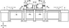
도 1은 본 발명의 일실시 형태에 의한 기판 검사 장치의 상면도이며, 도 2는 본 발명의 일실시 형태에 의한 기판 검사 장치의 측면도이다. 본 실시 형태는, 검사광이 기판의 결함에 의해 산란된 산란광으로부터 기판의 결함을 검출하는 기판 검사 장치의 예를 나타내고 있다. 기판 검사 장치는, 스테이지(10), 롤러(11), 프레임(13, 14), 광학 시스템 이동 기구, 광학 시스템 유닛(20a, 20b), 초점 조절 기구(41), 센서(51), 교정용 스테이지(61a, 61b) 및 제어 시스템을 포함해서 구성된다. 한편, 이하에 설명하는 실시 형태에 있어서의 XY 방향은 예시이며, X 방향과 Y 방향을 바꿀 수도 있다.FIG. 1 is a top view of a substrate inspection apparatus according to an embodiment of the present invention, and FIG. 2 is a side view of a substrate inspection apparatus according to an embodiment of the present invention. The present embodiment shows an example of a substrate inspection apparatus for detecting defects on a substrate from scattered light scattered by a defect in the substrate. The substrate inspection apparatus includes a
도 1 및 도 2에 있어서, 검사 대상인 복수의 기판(1)은, 라인 내에 있어서, 반입 컨베이어(2)에 의해 기판 검사 장치로 차례로 반입되며, 검사 후, 반출 컨베이어(3)에 의해 상기 기판 검사 장치로부터 차례로 반출된다. 스테이지(10)는, 반입 컨베이어(2)로부터 각 기판(1)을 받는다. 도 3은, 스테이지를 위쪽에서 바라본 상면도이다. 도 3에서 나타내듯이, 스테이지(10)의 양단부에 각각 직선 형상으로 마련된 롤러(11)는, 도 3에서 파선으로 나타낸 각 기판(1)의 이면의 주변부에 접촉하면서 회전하고, 각 기판(1)을 화살표로 나타내는 기판 이동 방향(X방향)으로 차례로 이동시킨다. 스테이지(10)의 상면에는, 도시하지 않은 복수의 에어 취출구가 마련되어 있다. 이들 복수의 에어 취출구는, 롤러(11)에 의해 이동되는 각 기판(1)의 이면에 대하여 에어를 내뿜도록 되어 있다. 각 기판(1)의 중앙부로 뿜어지는 에어의 작용에 의해, 각 기판(1)은 휘지 않고 부상되어, X 방향으로 차례로 이동한다.In Fig. 1 and Fig. 2, a plurality of
도 1 및 도 2에서 나타내듯이, 롤러(11)에 의해 X 방향으로 이동되는 기판(1)의 상방(도 1의 도면의 안길이 방향의 앞측, 도 2의 상측)에는, 기판(1)의 기판 이동 방향(X 방향)과 직교하는 방향(Y 방향)의 폭 이상으로 걸쳐서 연장되는 프레임(13, 14)이 설치된다. 이 프레임(13, 14)에는, 광학 시스템 유닛(20a, 20b)을 Y방향으로 이동시키는 광학 시스템 이동 기구가 탑재된다. 한편, 본 실시 형태에서는, 2개의 광학 시스템 유닛(20a, 20b)이 마련되어 있지만, 광학 시스템의 수는 이에 한하지 않고, 1개 또는 3개 이상의 광학 시스템을 마련할 수 있다.1 and 2, on the upper side of the substrate 1 (the front side in the direction of the drawing in Fig. 1, the upper side in Fig. 2) which is moved in the X direction by the
도 4는, 2개의 광학 시스템을 Y 방향으로 이동시키는 광학 시스템 이동 기구의 개략적 구성을 나타내는 일부 단면 측면도이다. 광학 시스템 이동 기구는, 가이드(15, 17), 이동대(16), 및 자석판(18)과 코일(19)로부터 이루어지는 리니어 모터를 포함하여 구성된다. 단면의 형상이 거의 L자 형상의 프레임(13, 14)에는, 도 4의 도면 안길이 방향(Y 방향)으로 연장되는 가이드(15)가 2개의 광학 시스템 유닛(20a, 20b)을 사이에 개재하듯이 마련되어 있다. 각각의 가이드(15)의 상측에는, 이동대(16)의 수납부(16c)가 탑재된다.4 is a partial sectional side view showing a schematic configuration of an optical system moving mechanism for moving two optical systems in the Y direction. The optical system moving mechanism includes
이동대(16)는, 광학 시스템 유닛(20a, 20b)을 수납하는 오목형의 수납부(16c)와, 이 수납부(16c)의 상단부에서 수평방향으로 연장되는 암부(16d)로 구성된다. 수납부(16c)에는, 후술하는 초점 조절 기구(41)를 통하여, 광학 시스템 유닛(20a, 20b)이 수납 탑재된다. 프레임(13)의 상면부 양측에는, 도 4 도면의 안길이 방향(Y 방향)으로 연장되는 가이드(17)가 마련되어 있다. 각각의 가이드(17)의 상측에는, 이동대(16)의 암부(16d)가 탑재된다.The movable table 16 is composed of a
프레임(13) 상면부의 중앙에는, 리니어 모터의 고정자인 자석판(18)이 설치되어 있다. 이동대(16)의 암부(16d)의 하측에는, 리니어 모터의 가동자인 코일(19)이 설치되어 있다. 후술하는 광학 시스템 이동 제어 회로(60)로부터 코일(19)로 전류를 흘리면, 코일(19)의 전류와 자석판(18)의 자기장으로부터, 플레밍(Fleming)의 왼손 법칙에 의해, 코일(19)에 추진력(로렌츠력)이 작용하여, 이동대(16)가 가이드(15) 및 가이드(17)를 따라 이동하고, 광학 시스템 유닛(20a, 20b)이 기판 이동 방향( X방향)과 직교하는 도면의 안길이 방향(Y 방향)으로 이동이 제어된다.A
도 5는, 광학 시스템 및 제어 시스템의 개략적 구성을 나타내는 도면이다. 광학 시스템 유닛(20a, 20b)은, 검사광을 기판(1)으로 조사하는 투광 시스템, 기판(1)으로부터의 반사광을 검출하는 반사광 검출 시스템, 및 기판(1)으로부터의 산란광을 수광하는 수광 시스템을 포함해서 구성된다. 또한, 제어 시스템은, 초점 조절 제어 회로(40), 신호 처리 회로(50), 광학 시스템 이동 제어 회로(60), 메모리(70), 통보 장치(80), 입출력장치(90) 및 CPU(100)를 포함해서 구성된다.5 is a diagram showing a schematic configuration of an optical system and a control system. The
도 6은, 광학 시스템의 투광 시스템 및 수광 시스템의 개략적 구성을 나타내는 사시도이다. 투광 시스템은, 레이저광원(21), 렌즈군(22) 및 미러(23)을 포함해서 구성된다. 레이저광원(21)은, 검사광이 되는 레이저광을 발생한다. 렌즈군(22)은, 레이저광원(21)으로부터 발생된 검사광을 집광하고, 집광된 검사광을 기판 이동 방향(X 방향)과 직교하는 방향(Y 방향)으로 넓히고, 넓힌 검사광을 기판 이동 방향(X 방향)으로 집속시킨다. 미러(23)는, 렌즈군(22)에 의해 집광된 검사광을, 기판(1)의 표면에 비스듬히 조사한다. 기판(1)의 표면에 조사된 검사광은, 기판(1)의 표면상에 있어서, 기판 이동 방향(X 방향)으로 집속되고, 기판 이동 방향(X 방향)과 직교하는 방향(Y 방향)으로 소정의 폭을 가진 길이가 긴 형상의 검사광이 된다. 기판(1)이 기판 이동 방향(X 방향)으로 이동하는 것에 의해, 투광 시스템으로부터 조사된 소정의 폭의 검사광이 기판(1)을 주사하게 되어, 주사 영역의 결함 검사가 실시된다.6 is a perspective view showing a schematic configuration of a light-transmitting system and a light-receiving system of the optical system. The light projecting system comprises a
기판(1)의 표면에 상처나 이물질 등의 결함이 존재하지 않을 경우, 기판(1)의 표면에 비스듬히 조사된 검사광의 일부는 기판(1)의 표면에서 반사되고, 나머지 검사광은 기판(1)의 내부를 투과해서 기판(1)의 이면에서 출사된다. 기판(1)의 표면에 상처나 이물질 등의 결함이 있을 경우는, 기판(1)의 표면에 조사된 검사광 안에서 기판 표면의 상처나 이물질 등의 결함에 조사된 광은 산란광이 되어 산란되고, 이외의 부분에 조사된 빛은 앞에서 얘기한 바와 같이, 일부는 표면에서 반사되고, 나머지는 투과된다.A portion of the inspection light obliquely irradiated on the surface of the
도 5에 있어서, 반사광 검출 시스템은, 미러(25), 렌즈(26), 및 CCD 라인 센서(27)를 포함해서 구성된다. 기판(1)의 표면으로부터의 반사광은, 미러(25)를 통해서 렌즈(26)에 입사된다. 렌즈(26)는, 기판(1)으로부터의 반사광을 집속시켜서, CCD 라인 센서(27)의 수광면에 결상시킨다.5, the reflected light detection system includes a
이 때, CCD 라인 센서(27)의 수광면에 있어서의 반사광의 수광 위치는, 기판(1) 표면의 높이에 의해 변화한다. 도 5에서 나타내는 기판(1)의 표면 높이를 기준으로 했을 때, 기판(1) 표면의 높이가 기준보다 낮을 경우, 기판(1)의 표면에서 검사광이 조사 및 반사되는 위치가 도면의 왼쪽으로 이동하고, CCD 라인 센서(27)의 수광면에 있어서의 반사광의 수광 위치가 도면의 오른쪽으로 이동한다. 반대로, 기판(1)의 표면의 높이가 기준보다 높을 경우, 기판(1)의 표면에서 검사광이 조사 및 반사되는 위치가 도면의 오른쪽으로 이동하고, CCD 라인 센서(27)의 수광면에 있어서의 반사광의 수광 위치가 도면의 왼쪽으로 이동한다.At this time, the light-receiving position of the reflected light on the light-receiving surface of the
CCD 라인 센서(27)는, 수광면에서 수광된 반사광의 강도에 따른 검출 신호를, 초점 조절 제어 회로(40)로 출력한다. 초점 조절 제어 회로(40)는, CPU(100)로부터의 지령에 따라, CCD 라인 센서(27)의 검출 신호에 근거하여, 기판(1)의 표면으로부터의 반사광이 CCD 라인 센서(27)의 수광면의 중심위치에서 수광되도록, 초점 조절 기구(41)를 구동해서 광학 시스템 유닛(20a, 20b)을 이동한다. 초점 조절 기구(41)는, 펄스 모터(42), 캠(43), 및 캠 폴로어(cam follower)(44)를 포함해서 구성된다. 펄스 모터(42)의 회전축에는, 편심된 캠(43)이 설치되어 있으며, 광학 시스템 유닛(20a, 20b)에는, 캠 폴로어(cam follower)(44)가 설치되어 있다. 초점 조절 제어 회로(41)로부터 펄스 모터(42)로 구동 펄스를 공급하는 것에 의해, 펄스 모터(42)가 구동되어 캠(43)이 회전하고, 광학 시스템 유닛(20a, 20b)이 상하로 이동되어, 광학 시스템 유닛(20a, 20b)의 초점 위치가 제어된다.The
도 6에 있어서, 수광 시스템은, 수광 렌즈(28), 결상 렌즈(29), 및 CCD 라인 센서(30)을 포함해서 구성된다. 집광 렌즈(28)는, 기판(1)으로부터의 산란광을 집광하고, 결상 렌즈(29)는, 집광 렌즈(28)로 집광한 산란광을 CCD 라인 센서(30)의 수광면에 결상시킨다. 도 5에 있어서, CCD 라인 센서(30)는, 수광면에서 수광한 산란광의 강도에 따른 검출 신호를 디지털 신호로 변환하여, 신호 처리 회로(50)로 출력한다.6, the light receiving system includes a
도 1 및 도 3에 있어서, 스테이지(10)에는, 광학 시스템 유닛(20a)의 투광 시스템으로부터의 검사광이 조사되는 영역에, 복수의 개구(12a)가 마련되며, 광학 시스템 유닛(20b)의 투광 시스템으로부터의 검사광이 조사되는 영역에, 복수의 개구(12b)가 마련되어 있다. 개구(12a)와 개구(12b)는, 기판 이동 방향(X 방향)과 직교하는 방향(Y 방향)에 있어서, 광학 시스템 유닛(20a, 20b)의 투광 시스템으로부터의 검사광의 폭 이상의 길이를 가지며, 다른 위치에 교대로 마련되어 있다. 도 4에 있어서, 광학 시스템 유닛(20a)의 투광 시스템으로부터 조사되어, 기판(1)의 내부를 투과해서 기판(1)의 이면으로부터 출사된 검사광은, 개구(12a)를 통해서 스테이지(10)의 하방으로 나아가고, 광학 시스템 유닛(20a)의 반사광 검출 시스템 및 수광 시스템으로 수광되지 않는다. 광학 시스템 유닛(20b)의 투광 시스템으로부터 조사되어, 기판(1)의 내부에 투과해서 기판(1)의 이면으로부터 출사된 검사광도, 동일하게, 개구(12b)를 통해서 스테이지(10)의 하방으로 나아가며, 광학 시스템 유닛(20b)의 반사광 검출 시스템 및 수광 시스템으로 수광되지 않는다.1 and 3, the
도 5에 있어서, 광학 시스템 이동 제어 회로(60)는, CPU(100)로부터의 지령을 따라, 코일(19)로 전류를 공급하고, 광학 시스템 유닛(20a, 20b)을 기판 이동 방향(X 방향)과 직교하는 방향(Y 방향)으로 이동하여, 광학 시스템 유닛(20a, 20b)의 투광 시스템으로부터의 소정의 폭의 검사광에 의해 주사되는 기판(1)의 주사 영역을 기판마다 변경한다.5, the optical system
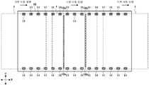
도 7은, 기판의 주사 영역을 나타내는 도면이다. 본 실시 형태는, 기판(1)의 검사 영역을 44개의 주사 영역으로 분할하고, 2개의 광학 시스템 유닛(20a, 20b)을 이용하여, 각각 22회씩 주사하는 예를 나타내고 있다. 또한, 주사 영역 수 및 주사 회수는, 이에 한하지 않고, 기판의 크기나 광학 시스템의 수에 따라서 적절히 결정된다.7 is a view showing a scanning region of the substrate. The present embodiment shows an example in which the inspection region of the
도 7에 있어서, 기판(1)의 주변부의 영역(NS)은, 롤러(11)가 접촉하는 검사 대상 이외의 영역이며, 영역(SA1~SA22, SB1~SB22)은, 광학 시스템 유닛(20a, 20b)의 주사 영역이다. 본 실시 형태에서는, 우선, 첫 번째 기판(1)이 후술하는 센서(51)의 하방에 도달하기 전에, 광학 시스템 유닛(20a)을 주사 영역(SA1)이 통과하는 위치의 상공으로 이동하고, 광학 시스템 유닛(20b)을 주사 영역(SB1)이 통과하는 위치의 상공으로 이동한다. 그리고 첫 번째 기판(1)에 대해서, 광학 시스템 유닛(20a)의 투광 시스템으로부터의 검사광에 의해, 주사 영역(SA1)의 주사가 실시되어, 광학 시스템 유닛(20b)의 투광 시스템으로부터의 검사광에 의해, 주사 영역(SB1)의 주사가 실시된다.7, the peripheral area NS of the
첫 번째 기판의 주사가 종료된 후, 두 번째 기판(1)이 후술하는 센서(51)의 하방에 도달하기 전에, 광학 시스템 유닛(20a)을 주사 영역(SA2)이 통과하는 위치의 상공으로 이동하고, 광학 시스템 유닛(20b)을 주사 영역(SB2)이 통과하는 위치의 상공으로 이동한다. 그리고 두 번째 기판(1)에 대해서, 광학 시스템 유닛(20a)의 투광 시스템으로부터의 검사광에 의해, 주사 영역(SA2)의 주사를 실시하고, 광학 시스템 유닛(20b)의 투광 시스템으로부터의 검사광에 의해, 주사 영역(SB2)의 주사를 실시한다. 이후, 이들 동작을 되풀이하고, 22번째 기판(1)에 대해서, 광학 시스템 유닛(20a)의 투광 시스템으로부터의 검사광에 의해, 주사 영역(SA22)의 주사를 실시하고, 광학 시스템 유닛(20b)의 투광 시스템으로부터의 검사광에 의해, 주사 영역(SB22)의 주사를 실시한다.After the scanning of the first substrate is completed, before the
22번째 기판(1)의 주사가 종료된 후에는, 처음으로 되돌아가, 23번째~44번째 기판(1)의 주사를, 첫 번째~22번째 기판(1)의 주사와 동일하게 실시할 수 있다. 혹은, 23번째 기판(1)의 주사를 22번째 기판(1)의 주사와 동일하게 실시한 후, 광학 시스템 유닛(20a, 20b)을 역방향으로 이동하고, 24번째~44번째 기판(1)의 주사를, 21번째~첫 번째 기판(1)의 주사와 동일하게 실시할 수 있다. 45번째 이후의 기판(1)의 주사도 같다.After the scanning of the
도 1 및 도 2에 있어서, 센서(51)는, 롤러(11)에 의해 이동되는 기판(1)의 기판 이동 방향 측의 가장자리를 검출하고, 검출 신호를 도 5의 신호 처리 회로(50)로 출력한다. 도 5에 있어서, 신호 처리 회로(50)는, CCD 라인 센서(30)로부터의 디지털 신호를 처리하고, 주사 영역의 기판(1)의 결함을, 미리 정한 크기의 랭크별로 검출하고, 검출한 결함의 주사 영역 내에서의 기판 이동 방향(X 방향)과 직교하는 방향(Y 방향)의 위치를 검출한다. 신호 처리 회로(50)는, 또한, 센서(51)로부터 검출 신호를 입력하고 나서의 경과 시간에 근거하여, 검출한 결함 기판의 이동 방향(X 방향)의 위치를 검출한다. 신호 처리 회로(50)는, 검출한 결함 데이터를, CPU(100)로 출력한다.1 and 2, the
도 5에 있어서, 메모리(70)는, CPU(100)의 제어에 의해, 신호 처리 회로(50)가 검출된 주사 영역의 기판(1)의 결함 데이터를, 주사 영역마다 기억한다. 통보 장치(80)는, CPU(100)의 제어에 의해, 후술하는 통보를 실시한다. 입출력장치(90)는, 후술하는 라인 정지 명령을 입력하고, 그리고 CPU(100)의 제어에 의해, 결함의 데이터 및 후술하는 판정 결과를 출력한다.5, the
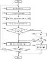
도 8은, 본 발명의 일실시 형태에 의한 기판 검사 장치의 동작을 나타내는 순서도이다. 우선, CPU(100)는, 광학 시스템 유닛(20a, 20b)의 이동을, 광학 시스템 이동 제어 회로(60)로 지령한다. 광학 시스템 이동 제어 회로(60)는, CPU(100)로부터의 지령을 따라, 코일(19)로 전류를 공급하고, 광학 시스템 유닛(20a, 20b)을 각각의 주사 영역이 통과하는 위치의 상공으로 이동한다(단계 101). 롤러(11)에 의한 기판(1)의 이동에 따라, 신호 처리 회로(50)는, CCD 라인 센서(30)로부터의 디지털 신호를 처리하고, 주사 영역의 기판(1)의 결함을 검출한다(단계 102).8 is a flowchart showing the operation of the substrate inspection apparatus according to the embodiment of the present invention. First, the
다음으로, CPU(100)는, 메모리(70)를 제어하고, 검출한 주사 영역의 기판 결함 데이터를, 주사 영역마다 기억하고, 기판마다, 신호 처리 회로(50)가 새로이 검출된 주사 영역의 기판(1) 결함 데이터에 의해, 메모리(70)에 기억된 같은 주사 영역의 기판(1)의 결함 데이터를 갱신한다(단계 103). 그리고 CPU(100)는, 기판마다, 메모리(100)에 기억된 복수의 주사 영역의 기판(1)의 결함 데이터로부터, 기판 한 장분의 결함 데이터를 작성한다(단계 104).Next, the
다음으로, CPU(100)는, 작성한 기판 한 장분의 결함 데이터에 근거하여, 기판마다, 기판 한 장분의 결함 수가 허용 값 이내인지 아닌지를 판정한다(단계 105). 이러한 판정은, 결함 크기의 랭크별로 실시할 수도 있고, 혹은 결함 크기의 랭크에 관계없이 기판 한 장분의 모든 결함을 대상으로 실시할 수도 있다. 기판 한 장분의 결함 수가 허용 값 이내였을 경우, 단계 109로 넘어간다. 기판 한 장분의 결함 수가 허용 값을 넘었을 경우, CPU(100)는, 통보 장치(80)를 제어하고, 라인 관리자 또는 라인 제어 설비로, 기판 한 장분의 결함 수가 허용 값을 넘었다는 취지를 통보한다(단계 106). 이어서, CPU(100)는, 라인 관리자 또는 라인 제어 설비로부터 입출력 장치(90)로 라인 정지 명령이 입력된 것인지 아닌지를 판정한다(단계 107). 라인 정지 명령이 입력되지 않을 경우, 단계 109로 넘어간다. 라인 정지 명령이 입력되었을 경우, CPU(100)는, 입출력장치(90)를 제어하고, 결함 데이터 및 판정 결과를 출력하고(단계 108), 처리를 멈춘다.Next, the
그 다음, CPU(100)는, 입출력장치(90)를 제어하여, 기판마다, 결함 데이터 및 판정 결과를 출력한다(단계 109). 결함의 데이터의 출력은, 예를 들면, 결함의 크기 및 위치를 나타내는 맵을, 모니터용 디스플레이로 표시하면서 프린터로 인쇄하거나, 혹은, 결함 크기의 랭크별로, 각 주사 영역의 결함 수 및 기판 한 장분의 결함 수를, 모니터용 디스플레이로 표시하면서 프린터로 인쇄하여 실시한다. 계속해서, CPU(100)는, 전 기판의 검사가 종료되었는지 여부를 판정하고(단계 110), 종료되지 않은 경우는 단계 101로 되돌아가고, 종료되었을 경우는 처리를 멈춘다.Then, the
이상, 설명한 실시 형태에 의하면, 검출한 주사 영역의 기판 결함 데이터를, 주사 영역마다 기억하고, 기판마다, 새로이 검출한 주사 영역의 기판 결함 데이터에 의해, 기억된 동일한 주사 영역의 기판 결함 데이터를 갱신해서(단계 103), 복수의 주사 영역의 기판 결함 데이터로부터, 기판 한 장분의 결함 데이터를 작성하는(단계 104) 것에 의해, 기판 한 장분의 결함의 데이터를 기판마다 얻을 수 있으므로, 라인 내에서의 기판의 결함 검사를 보다 신속하게 실시할 수 있다.According to the embodiments described above, the substrate defect data of the detected scan area is stored for each scan area, and the substrate defect data of the same scan area stored by the substrate defect data of the newly detected scan area is updated (Step 103), defect data for one sheet of the substrate can be obtained for each substrate by generating defect data for one sheet from the substrate defect data of the plurality of scan areas (step 104), and therefore, The defect inspection of the substrate can be performed more quickly.
나아가, 이상 설명한 실시 형태에 의하면, 작성한 기판 한 장분의 결함의 데이터에 근거하여, 기판마다, 기판 한 장분의 결함 수가 허용 값 이내인지 아닌지를 판정하는(단계 105) 것에 의해, 기판 한 장분의 결함 수가 허용 값을 넘는 불량이 발생했을 경우, 불량을 기판마다 조기에 발견할 수 있다.Further, according to the embodiment described above, it is judged whether or not the number of defects per one substrate is within the permissible value for each substrate (step 105), based on the defect data for one substrate, If the number of defects exceeding the permissible value occurs, defects can be detected early for each substrate.
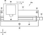
도 9 및 도 10은, 도 1 및 도 2의 교정용 스테이지의 개략적 구성을 나타내는 도면이며, 도 9는 도 1에 대응하는 상면도를 나타내고, 도 10은 도 2에서 나타내는 교정 스테이지를 왼쪽에서 바라본 측면도를 나타낸다. 교정 스테이지(61a)는, 도 1에서 나타내듯이, 스테이지(10)의 하측의 메인테넌스(maintenance) 영역 내에 있으며, 프레임(13, 14)의 다리 위에 설치된다. 교정 스테이지(61a)는, 베이스(61, 68), 조정 볼트(62), 볼나사 유닛(63), 서보 모터(64), 샘플 홀더(65), 표준 입자 부착 기판(66), 가동 블록(67) 및 판 스프링(69)으로 구성된다. 표준 입자 부착 기판(66)은, 샘플 홀더(65)에 세팅된다. 표준 입자 부착 기판(66)은 샘플 홀더(65)에 마련된 판 스프링(69)에 의해, 지지된다. 샘플 홀더(65)는, 볼나사 유닛(63)의 가동 블록(67) 상에 설치되어, 서보 모터(64)가 회전하는 것에 의해 직선 이동을 한다. 볼나사 유닛(63)은, 기판 이동 방향과 나란히 설치함으로써, 가동 블록(67) 상의 샘플 홀더(65)도 평행하게 이동하는 것이 가능해진다.9 and 10 are views showing a schematic configuration of the calibration stage of Figs. 1 and 2, Fig. 9 shows a top view corresponding to Fig. 1, Fig. 10 shows a calibration stage shown in Fig. Fig. The
볼나사 유닛(63)은, 베이스(61) 상에 고정되어 있으며, 베이스(61)는 3개의 조정 볼트(62)에 의해, 장치의 다리 위에 설치된 베이스(68)와의 틈에서 두 방향으로 조정이 가능하도록 되어 있다. 이에 의해, 기판 이동 방향으로 이동 중인 기판(1)의 표면과 표준 입자 부착 기판(66)의 표면 높이가 동일하게 되도록 높이를 조정하는 것이 가능하다.The
광학 시스템의 교정 작업은, 오퍼레이터가 조작 패널을 조작해서 검사 모드를 교정 모드로 전환하는 것에 의해 실시된다. 이에 의해, 광학 시스템 유닛(20a, 20b)은 -Y 방향으로 동작하고, 메인테넌스(maintenance) 영역으로 이동한다. 광학 시스템 유닛(20a, 20b)은, 메인테넌스(maintenance) 영역 내의 표준 입자 부착 기판(66) 상의 검사 시작 위치까지 이동한 후, 정지하여, 표준 입자 부착 기판(66)의 검사 개시 대기 상태가 된다. 교정용 스테이지(61a)가 검사 영역 내의 기판 이동 방향과 같은 방향, 같은 속도로 X 방향으로 이동을 시작하면 광학 시스템 유닛(20a, 20b)이 표준 입자 부착 기판(66)의 주사를 실시한다. 교정용 스테이지(61a, 6lb)의 X 방향으로의 동작 완료 후, 광학 시스템 유닛(20a, 20b)은 다음 주사 준비를 하기 위해서 Y 방향으로 주사 피치만큼 이동한다. 교정용 스테이지(61a, 6lb)는 검사 시작 위치까지 X 방향으로 되돌아와 동작을 실시한다.The calibration of the optical system is performed by the operator operating the operation panel to switch the test mode to the calibration mode. Thereby, the
교정용 스테이지(61a, 6lb)의 검사 개시 위치까지 X 방향으로 되돌아가는 동작 완료 후, 교정용 스테이지(61a, 6lb)가 검사 영역 내의 기판 이동 방향과 같은 방향, 같은 속도로 X 방향으로 이동하여 광학 시스템 유닛(20a, 20b)이 표준 입자 부착 기판(66)의 주사를 실시하고, 검사를 완료한다. 이 검사 결과에 근거하여 오퍼레이터는, 레이저 파워의 확인, 감도 조정 작업을 실시한다. 교정 작업 중은, 제조 라인 내에 사람이 억지로 들어갈 필요가 없기 때문에, 라인 가동 중에 있어서도 이 교정 작업을 실시하는 것이 가능해진다. 한편, 이 실시 형태에서는, 교정 스테이지(61a, 6lb)가 배치되는 곳이 메인테넌스(maintenance) 영역이며, 기판(1)이 이동하는 영역이 검사 영역이다.After completion of the operation to return to the inspection start position of the calibration stages 61a and 61b, the calibration stages 61a and 61b move in the X direction at the same speed in the same direction as the substrate moving direction in the inspection area, The
본 실시 예에서는, 메인테넌스(maintenance) 영역을 프레임단이 한군데인 경우를 설명하였으나, 광학 시스템 유닛이 프레임 상에 두 대 탑재될 경우에는, 메인테넌스(maintenance) 영역을 프레임 양단의 2군데에 마련하고, 교정용 스테이지를 설치하는 것도 가능하다. 이 경우, 한 대의 광학 시스템 유닛은 검사 영역 내에서 제조 라인을 흐르는 기판의 검사를 실시하고, 다른 한 대의 광학 시스템 유닛은 교정 작업을 실시하는 것도 가능하다.In the present embodiment, the case where the maintenance area is one frame is described. However, when two optical system units are mounted on the frame, the maintenance area is divided into two areas at both ends of the frame And it is also possible to provide a calibration stage. In this case, it is also possible that one optical system unit inspects the substrate flowing through the production line in the inspection region, and the other optical system unit performs the correction operation.
상기에서는 본 발명의 실시예들을 참조하여 설명하였지만, 해당 기술 분야에서 통상의 지식을 가진 자라면 하기의 특허 청구 범위에 기재된 본 발명의 사상 및 영역으로부터 벗어나지 않는 범위 내에서 본 발명을 다양하게 수정 및 변경시킬 수 있음을 이해할 수 있을 것이다.While the present invention has been particularly shown and described with reference to exemplary embodiments thereof, it is to be understood that the invention is not limited to the disclosed exemplary embodiments, and variations and modifications may be made without departing from the scope of the invention. It will be understood that the present invention can be changed.
1 : 기판 2 : 반입 컨베이어
3 : 반출 컨베이어 10 : 스테이지
11 : 롤러 12a, 12b : 개구
13, 14 : 프레임 15, 17 : 가이드
16 : 이동대 18 : 자석판(리니어 모터의 고정자)
19 : 코일(리니어 모터의 가동자) 20a, 20b : 광학 시스템
21 : 레이저 광원 22 : 렌즈군
23, 25 : 미러 26 : 렌즈
27 : CCD 라인 센서 28 : 집광 렌즈
29 : 결상 렌즈 30 : CCD 라인 센서
40 : 초점 조절 제어 회로 41 : 초점 조절 기구
42 : 펄스 모터 43 : 캠
44 : 캠 폴로어(cam follower) 50 : 신호 처리 회로
51 : 센서 60 : 광학 시스템 이동 제어 회로
61a, 6lb : 교정용 스테이지 70 : 메모리
80 : 통보 장치 90 : 입출력장치
100 : CPU1: substrate 2: carry-in conveyor
3: Dispensing conveyor 10: Stage
11:
13, 14:
16: moving base 18: magnetic plate (stator of linear motor)
19: coils (mover of linear motor) 20a, 20b: optical system
21: laser light source 22: lens group
23, 25: mirror 26: lens
27: CCD line sensor 28: condensing lens
29: image forming lens 30: CCD line sensor
40: Focus adjustment control circuit 41: Focus adjustment mechanism
42: Pulse motor 43: Cam
44: cam follower 50: signal processing circuit
51: sensor 60: optical system movement control circuit
61a, 61b: calibration stage 70: memory
80: Notification device 90: Input / output device
100: CPU
Claims (10)
Translated fromKorean기판 이동 수단에 의해 이동 중인 상기 기판과 직교하는 방향으로 투광 시스템 및 수광 시스템으로 이루어지는 광학 시스템을 이동시켜서 검사광을 조사함과 동시에 상기 기판으로부터의 반사광 또는 산란광을 수광하고,
수광된 상기 기판으로부터의 반사광 또는 산란광에 근거하여 상기 기판의 결함을 검사하는 인라인 기판 검사 장치의 광학 시스템 교정 방법에 있어서,
상기 기판의 검사가 실시되는 검사 영역 이외의 장소에 교정 작업 영역을 마련하고, 상기 광학 시스템을 상기 교정 작업 영역으로 이동이 가능하도록 하고, 상기 기판의 이동 중에 상기 광학 시스템의 교정 작업을 상기 교정 작업 영역에서 실시하도록 한 것을 특징으로 하는 인라인 기판 검사 장치의 광학 시스템 교정 방법.While sequentially moving the substrate in the horizontal direction from the upstream line to the downstream line,
The optical system including the light projecting system and the light receiving system is moved by the substrate moving means in the direction orthogonal to the substrate being moved to irradiate the inspection light and receive reflected light or scattered light from the substrate,
An optical system calibrating method of an in-line substrate inspecting apparatus for inspecting defects of a substrate based on reflected light or scattered light from the substrate,
A calibration work area is provided at a location other than the inspection area where the inspection of the substrate is performed so that the optical system can be moved to the calibration work area and the calibration work of the optical system is performed during the movement of the substrate, Wherein the optical system calibration method is performed in a region where the optical system is to be inspected.
투광 시스템 및 수광 시스템을 갖는 광학 시스템을 상기 기판의 이동 방향과 직교하는 방향으로 이동시켜, 상기 투광 시스템으로부터의 기판 이동 방향과 직교하는 방향에 소정의 폭을 갖는 검사광에 의해 주사되는 기판의 주사 영역을 기판마다 변경하고,
상기 투광 시스템으로부터 기판 이동 방향과 직교하는 방향에 소정의 폭을 갖는 검사광을 상기 기판으로 조사하고,
상기 수광 시스템이 수광한 광의 강도로부터, 주사 영역의 기판의 결함을 검출하고,
검출한 주사 영역의 기판 결함 데이터를, 주사 영역마다 기억하고,
기판마다, 새로이 검출된 주사 영역의 기판 결함 데이터에 의해, 기억된 동일한 주사 영역의 기판 결함 데이터를 갱신하고, 복수의 주사 영역의 기판 결함 데이터로부터, 기판 한 장분의 결함 데이터를 작성하는 인라인 기판 검사 장치의 광학 시스템 교정 방법에 있어서,
상기 기판의 검사가 행하여지는 검사 영역 이외의 장소에 교정 작업 영역을 마련하고, 상기 광학 시스템을 상기 교정 작업 영역으로 이동이 가능하도록 하여, 상기 기판의 이동 중에 상기 광학 시스템의 교정 작업을 상기 교정 작업 영역에서 실시되도록 한 것을 특징으로 하는 인라인 기판 검사 장치의 광학 시스템 교정 방법.While sequentially moving the substrate from the upstream line to the downstream line in the horizontal direction,
The optical system having the light projecting system and the light receiving system is moved in the direction orthogonal to the moving direction of the substrate and the scanning of the substrate scanned by the inspection light having the predetermined width in the direction orthogonal to the substrate moving direction from the light projecting system Area is changed for each substrate,
Irradiating the substrate with inspection light having a predetermined width in a direction orthogonal to the substrate moving direction from the light projection system,
Detecting a defect in the substrate in the scan area from the intensity of the light received by the light receiving system,
The substrate defect data of the detected scan area is stored for each scan area,
The substrate defect data of the same scan area stored by the substrate defect data in the newly detected scan area is updated for each substrate and the inline substrate inspection for creating defect data of one substrate from the substrate defect data of the plurality of scan areas A method of calibrating an optical system of an apparatus,
A calibration work area is provided at a place other than the inspection area in which the inspection of the substrate is performed so that the optical system can be moved to the calibration work area and the calibration work of the optical system during the movement of the substrate is performed by the calibration work Wherein the optical system calibration is performed in a region where the optical system is mounted.
상기 기판의 이동 방향과 같은 방향 및 같은 속도로 이동하는 광학 시스템 교정용 표준 입자 부착 기판을 상기 교정 작업 영역 내에 마련하고, 상기 광학 시스템을 상기 교정 작업 영역으로 이동하여, 상기 기판의 이동 중에 상기 광학 시스템 교정용 표준 입자 부착 기판을 검사함으로써 상기 광학 시스템의 교정 작업을 실시하도록 한 것을 특징으로 하는 인라인 기판 검사 장치의 광학 시스템 교정 방법.3. The method according to claim 1 or 2,
A standard particle mounting substrate for calibration of an optical system moving in the same direction and at the same speed as the moving direction of the substrate is provided in the calibration working area and the optical system is moved to the calibration working area, Wherein the optical system is calibrated by inspecting a standard particle-attached substrate for system calibration.
상기 광학 시스템 교정용 표준 입자 부착 기판을 상기 검사 영역 내의 기판 높이에 맞추는 높이 조정 수단을 구비한 것을 특징으로 하는 인라인 기판 검사 장치의 광학 시스템 교정 방법.The method of claim 3,
And a height adjusting means for adjusting the standard particle mounting substrate for optical system calibration to the height of the substrate in the inspection region.
작성한 기판 한 장분의 결함 데이터에 근거하여, 기판마다, 기판 한 장분의 결함 수가 허용 값 이내인지 아닌지를 판정하는 것을 특징으로 하는 인라인 기판 검사 장치의 광학 시스템 교정 방법.3. The method of claim 2,
And judges whether or not the number of defects per one substrate is within a permissible value for each substrate, based on the defect data of the prepared one substrate.
상기 기판 이동 수단에 의해 이동 중의 상기 기판에 대하여 검사광을 조사하는 투광 시스템, 및 상기 기판으로부터의 반사광 또는 산란광을 수광하는 수광 시스템을 갖는 광학 시스템과,
상기 광학 시스템을 상기 기판의 이동 방향과 직교하는 방향으로 이동시켜서 상기 기판으로부터의 반사광 또는 산란광에 근거하여 상기 기판의 결함을 검사하는 검사 수단으로 이루어지는 인라인 기판 검사 장치에 있어서,
상기 검사 수단에 의해 상기 기판의 검사가 실시되는 검사 영역 이외의 장소에 교정 작업 영역을 마련하고, 상기 광학 시스템을 상기 교정 작업 영역으로 이동이 가능하도록 하고, 상기 기판의 이동 중에 상기 광학 시스템의 교정 작업을 상기 교정 작업 영역에서 실시하도록 한 것을 특징으로 하는 인라인 기판 검사 장치.Substrate moving means for sequentially moving the substrate in the horizontal direction from the upstream line to the downstream line,
An optical system having a light projecting system for irradiating inspection light onto the substrate while being moved by the substrate moving means, and a light receiving system for receiving reflected light or scattered light from the substrate,
And inspecting means for inspecting defects of the substrate based on reflected light or scattered light from the substrate by moving the optical system in a direction perpendicular to the moving direction of the substrate,
A calibration work area is provided at a place other than the inspection area where the inspection of the substrate is performed by the inspection means so that the optical system can be moved to the calibration work area, And the operation is performed in the calibration work area.
상기 기판 이동 수단에 의해 이동 중의 기판에 대하여 검사광을 조사하는 투광 시스템, 및 상기 기판으로부터의 반사광 또는 산란광을 수광하는 수광 시스템을 갖는 광학 시스템과,
상기 광학 시스템을 기판 이동 방향과 직교하는 방향으로 이동하여, 상기 투광 시스템으로부터의 검사광에 의해 주사되는 기판의 주사 영역을 기판마다 변경하는 광학 시스템 이동 수단과,
상기 수광 시스템이 수광한 광의 강도로부터, 주사 영역의 기판의 결함을 검출하는 처리 수단과,
상기 처리 수단이 검출한 주사 영역의 기판 결함 데이터를, 주사 영역마다 기억하는 기억 수단과,
상기 기억 수단을 제어하고, 기판마다, 상기 처리 수단이 새로이 검출한 주사 영역의 기판 결함 데이터에 의해, 상기 기억 수단에 기억된 같은 주사 영역의 기판 결함 데이터를 갱신하여, 상기 기억 수단에 기억된 복수의 주사 영역의 기판 결함 데이터로부터, 기판 한 장분의 결함 데이터를 작성하는 제어 수단으로 이루어지는 인라인 기판 검사 장치에 있어서,
상기 기판의 검사가 실시되는 검사 영역 이외의 장소에 교정 작업 영역을 마련하고, 상기 광학 시스템을 상기 교정 작업 영역으로 이동이 가능하도록 하여, 상기 기판의 이동 중에 상기 광학 시스템의 교정 작업을 상기 교정 작업 영역에서 실시하도록 한 것을 특징으로 하는 상기 인라인 기판 검사 장치.Substrate moving means for sequentially moving the substrate horizontally from the upstream line to the downstream line,
An optical system having a light projecting system for irradiating inspection light onto the substrate while being moved by the substrate moving means, and a light receiving system for receiving reflected light or scattered light from the substrate,
Optical system moving means for moving the optical system in a direction orthogonal to the substrate moving direction to change a scanning area of the substrate scanned by the inspection light from the light projecting system for each substrate;
Processing means for detecting a defect in the substrate in the scanning region from the intensity of the light received by the light receiving system,
Storage means for storing, for each scan region, substrate defect data of the scan region detected by the processing means;
The control means controls the storage means to update the substrate defect data of the same scan region stored in the storage means with the substrate defect data of the scan region newly detected by the processing means for each substrate, And a control means for generating defect data of one sheet of the substrate from the substrate defect data of the scan region of the substrate,
A calibration work area is provided at a location other than the inspection area where the inspection of the substrate is performed and the optical system is allowed to move to the calibration work area so that the calibration work of the optical system during the movement of the substrate is performed by the calibration work Wherein the inspection is carried out in the region of the substrate.
상기 기판의 이동 방향과 같은 방향 및 같은 속도로 이동하는 광학 시스템 교정용 표준 입자 부착 기판을 상기 교정 작업 영역 내에 마련하여, 상기 광학 시스템을 상기 교정 작업 영역으로 이동하여, 상기 기판의 이동 중에 상기 광학 시스템 교정용 표준 입자 부착 기판을 검사함으로써 상기 광학 시스템의 교정 작업을 실시하도록 한 것을 특징으로 하는 인라인 기판 검사 장치.8. The method according to claim 6 or 7,
A standard particle mounting substrate for optical system calibration moving in the same direction and at the same speed as the moving direction of the substrate is provided in the calibration working area to move the optical system to the calibration working area, Wherein the optical system is calibrated by inspecting a standard particle-attached substrate for system calibration.
상기 광학 시스템 교정용 표준 입자 부착 기판을 상기 검사 영역 내의 기판 높이에 맞추는 높이 조정 수단을 구비한 것을 특징으로 하는 인라인 기판 검사 장치.9. The method of claim 8,
And height adjusting means for adjusting the standard particle mounting substrate for optical system calibration to the height of the substrate in the inspection region.
상기 제어 수단은, 작성한 기판 한 장분의 결함 데이터에 근거하여, 기판마다, 기판 한 장분의 결함 수가 허용 값 이내인지 아닌지를 판정하는 것을 특징으로 하는 인라인 기판 검사 장치.8. The method of claim 7,
Wherein said control means judges whether or not the number of defects for one sheet of the substrate is within a permissible value for each substrate based on defect data of one substrate prepared.
Applications Claiming Priority (2)
| Application Number | Priority Date | Filing Date | Title |
|---|---|---|---|
| JPJP-P-2009-227070 | 2009-09-30 | ||
| JP2009227070AJP2011075401A (en) | 2009-09-30 | 2009-09-30 | Method for calibrating optical system of in-line substrate inspection device and in-line substrate inspection device |
Publications (2)
| Publication Number | Publication Date |
|---|---|
| KR20110035845A KR20110035845A (en) | 2011-04-06 |
| KR101138041B1true KR101138041B1 (en) | 2012-04-23 |
Family
ID=43886249
Family Applications (1)
| Application Number | Title | Priority Date | Filing Date |
|---|---|---|---|
| KR1020100074553AExpired - Fee RelatedKR101138041B1 (en) | 2009-09-30 | 2010-08-02 | Optical system calibration method of in-line substrate inspection apparatus and inspection apparatus of in-line substrate |
Country Status (4)
| Country | Link |
|---|---|
| JP (1) | JP2011075401A (en) |
| KR (1) | KR101138041B1 (en) |
| CN (1) | CN102033069B (en) |
| TW (1) | TW201111773A (en) |
Cited By (1)
| Publication number | Priority date | Publication date | Assignee | Title |
|---|---|---|---|---|
| WO2015199930A1 (en)* | 2014-06-27 | 2015-12-30 | Applied Materials, Inc. | Linear inspection system |
Families Citing this family (2)
| Publication number | Priority date | Publication date | Assignee | Title |
|---|---|---|---|---|
| JP6919779B2 (en)* | 2016-12-20 | 2021-08-18 | 日本電気硝子株式会社 | Glass substrate manufacturing method |
| CN114184617A (en)* | 2021-12-07 | 2022-03-15 | 创新奇智(北京)科技有限公司 | Detection device |
Citations (3)
| Publication number | Priority date | Publication date | Assignee | Title |
|---|---|---|---|---|
| KR970003750A (en)* | 1990-10-17 | 1997-01-28 | 가나이 쯔또무 | Semiconductor production method and manufacturing equipment |
| KR970024399A (en)* | 1995-10-31 | 1997-05-30 | 김광호 | Laser beam generator with output calibration function and output calibration method |
| KR20040032766A (en)* | 2002-10-09 | 2004-04-17 | 가부시키가이샤 토프콘 | Surface inspection method and apparatus |
Family Cites Families (10)
| Publication number | Priority date | Publication date | Assignee | Title |
|---|---|---|---|---|
| US3970857A (en)* | 1975-08-06 | 1976-07-20 | E. I. Du Pont De Nemours And Company | Apparatus for web defect detection including a web swatch that contains a defect |
| JP2001110861A (en)* | 1999-10-06 | 2001-04-20 | Seiko Epson Corp | Semiconductor film inspection method, thin film transistor manufacturing method, and semiconductor film inspection apparatus |
| JP2001255232A (en)* | 2000-03-10 | 2001-09-21 | Micronics Japan Co Ltd | Inspection device for display panel substrate |
| JP2001343284A (en)* | 2000-06-01 | 2001-12-14 | Dainippon Printing Co Ltd | Calibration device and method |
| JP4203290B2 (en)* | 2002-09-27 | 2008-12-24 | 大日本印刷株式会社 | Display member color measuring method and apparatus |
| JP2005114458A (en)* | 2003-10-06 | 2005-04-28 | Dainippon Printing Co Ltd | Detection apparatus and detection method |
| KR100525312B1 (en)* | 2003-11-28 | 2005-11-23 | 삼성코닝정밀유리 주식회사 | Method for measuring particles of a glass substrate |
| JP4480002B2 (en)* | 2004-05-28 | 2010-06-16 | Hoya株式会社 | Nonuniformity defect inspection method and apparatus, and photomask manufacturing method |
| JP4951271B2 (en)* | 2005-05-12 | 2012-06-13 | オリンパス株式会社 | Board inspection equipment |
| JP5493256B2 (en)* | 2007-09-11 | 2014-05-14 | 凸版印刷株式会社 | Inspection jig for defect detection function in color filter visual inspection equipment |
- 2009
- 2009-09-30JPJP2009227070Apatent/JP2011075401A/ennot_activeCeased
- 2010
- 2010-08-02KRKR1020100074553Apatent/KR101138041B1/ennot_activeExpired - Fee Related
- 2010-08-02TWTW099125601Apatent/TW201111773A/enunknown
- 2010-08-04CNCN201010246306.7Apatent/CN102033069B/ennot_activeExpired - Fee Related
Patent Citations (3)
| Publication number | Priority date | Publication date | Assignee | Title |
|---|---|---|---|---|
| KR970003750A (en)* | 1990-10-17 | 1997-01-28 | 가나이 쯔또무 | Semiconductor production method and manufacturing equipment |
| KR970024399A (en)* | 1995-10-31 | 1997-05-30 | 김광호 | Laser beam generator with output calibration function and output calibration method |
| KR20040032766A (en)* | 2002-10-09 | 2004-04-17 | 가부시키가이샤 토프콘 | Surface inspection method and apparatus |
Cited By (4)
| Publication number | Priority date | Publication date | Assignee | Title |
|---|---|---|---|---|
| WO2015199930A1 (en)* | 2014-06-27 | 2015-12-30 | Applied Materials, Inc. | Linear inspection system |
| KR20170132912A (en)* | 2014-06-27 | 2017-12-04 | 어플라이드 머티어리얼스, 인코포레이티드 | Linear inspection system |
| KR101804331B1 (en) | 2014-06-27 | 2017-12-04 | 어플라이드 머티어리얼스, 인코포레이티드 | Linear inspection system |
| KR102139218B1 (en) | 2014-06-27 | 2020-07-29 | 어플라이드 머티어리얼스, 인코포레이티드 | Linear inspection system |
Also Published As
| Publication number | Publication date |
|---|---|
| CN102033069B (en) | 2014-03-26 |
| JP2011075401A (en) | 2011-04-14 |
| CN102033069A (en) | 2011-04-27 |
| KR20110035845A (en) | 2011-04-06 |
| TW201111773A (en) | 2011-04-01 |
Similar Documents
| Publication | Publication Date | Title |
|---|---|---|
| JP5863547B2 (en) | Printed circuit board inspection equipment | |
| KR101039020B1 (en) | Board inspection apparatus and board inspection method | |
| JP5444053B2 (en) | Polycrystalline silicon thin film inspection method and apparatus | |
| CN101308099A (en) | Optical inspection device | |
| KR20090033031A (en) | Board appearance inspection device | |
| KR101917131B1 (en) | Optical inspecting apparatus | |
| KR101138041B1 (en) | Optical system calibration method of in-line substrate inspection apparatus and inspection apparatus of in-line substrate | |
| CN116149037A (en) | Ultrafast large-size scanning system and method | |
| KR20110111237A (en) | Repair device | |
| JP2012163370A (en) | In-line substrate inspection method and device | |
| JP2013044578A (en) | Substrate inspection method and device | |
| JP4693581B2 (en) | Substrate inspection apparatus and substrate inspection method | |
| KR20120017527A (en) | Laser processing equipment and its control method | |
| JP2001044136A (en) | Precision laser beam irradiation apparatus and control method | |
| KR20100058269A (en) | Camera module apparatus | |
| JP5178281B2 (en) | Substrate inspection apparatus and substrate inspection method | |
| JP5250395B2 (en) | Inspection device | |
| JP4994053B2 (en) | Substrate inspection apparatus and substrate inspection method | |
| JP2011226939A (en) | Method and device for inspecting substrate | |
| JP4708292B2 (en) | Substrate inspection apparatus and substrate inspection method | |
| JP2006194755A (en) | Substrate inspection apparatus and substrate inspection method | |
| KR100748108B1 (en) | Inspection device for cathode ray tube panel and method | |
| JP2012127761A (en) | Substrate inspection device | |
| JP2011069676A (en) | Inspection system, and inspection method | |
| JP2014044094A (en) | Substrate inspection method and device |
Legal Events
| Date | Code | Title | Description |
|---|---|---|---|
| A201 | Request for examination | ||
| PA0109 | Patent application | St.27 status event code:A-0-1-A10-A12-nap-PA0109 | |
| PA0201 | Request for examination | St.27 status event code:A-1-2-D10-D11-exm-PA0201 | |
| PG1501 | Laying open of application | St.27 status event code:A-1-1-Q10-Q12-nap-PG1501 | |
| PE0902 | Notice of grounds for rejection | St.27 status event code:A-1-2-D10-D21-exm-PE0902 | |
| P11-X000 | Amendment of application requested | St.27 status event code:A-2-2-P10-P11-nap-X000 | |
| P13-X000 | Application amended | St.27 status event code:A-2-2-P10-P13-nap-X000 | |
| R17-X000 | Change to representative recorded | St.27 status event code:A-3-3-R10-R17-oth-X000 | |
| E701 | Decision to grant or registration of patent right | ||
| PE0701 | Decision of registration | St.27 status event code:A-1-2-D10-D22-exm-PE0701 | |
| GRNT | Written decision to grant | ||
| PR0701 | Registration of establishment | St.27 status event code:A-2-4-F10-F11-exm-PR0701 | |
| PR1002 | Payment of registration fee | St.27 status event code:A-2-2-U10-U11-oth-PR1002 Fee payment year number:1 | |
| PG1601 | Publication of registration | St.27 status event code:A-4-4-Q10-Q13-nap-PG1601 | |
| R17-X000 | Change to representative recorded | St.27 status event code:A-5-5-R10-R17-oth-X000 | |
| LAPS | Lapse due to unpaid annual fee | ||
| PC1903 | Unpaid annual fee | St.27 status event code:A-4-4-U10-U13-oth-PC1903 Not in force date:20150413 Payment event data comment text:Termination Category : DEFAULT_OF_REGISTRATION_FEE | |
| PC1903 | Unpaid annual fee | St.27 status event code:N-4-6-H10-H13-oth-PC1903 Ip right cessation event data comment text:Termination Category : DEFAULT_OF_REGISTRATION_FEE Not in force date:20150413 | |
| P22-X000 | Classification modified | St.27 status event code:A-4-4-P10-P22-nap-X000 | |
| R18-X000 | Changes to party contact information recorded | St.27 status event code:A-5-5-R10-R18-oth-X000 |