KR101137930B1 - 3d-nonvolatile memory device and method for manufacturing the same - Google Patents
3d-nonvolatile memory device and method for manufacturing the sameDownload PDFInfo
- Publication number
- KR101137930B1 KR101137930B1KR1020100041448AKR20100041448AKR101137930B1KR 101137930 B1KR101137930 B1KR 101137930B1KR 1020100041448 AKR1020100041448 AKR 1020100041448AKR 20100041448 AKR20100041448 AKR 20100041448AKR 101137930 B1KR101137930 B1KR 101137930B1
- Authority
- KR
- South Korea
- Prior art keywords
- channel
- selection line
- forming
- selection
- film
- Prior art date
- Legal status (The legal status is an assumption and is not a legal conclusion. Google has not performed a legal analysis and makes no representation as to the accuracy of the status listed.)
- Expired - Fee Related
Links
Images


Classifications
- H—ELECTRICITY
- H10—SEMICONDUCTOR DEVICES; ELECTRIC SOLID-STATE DEVICES NOT OTHERWISE PROVIDED FOR
- H10B—ELECTRONIC MEMORY DEVICES
- H10B43/00—EEPROM devices comprising charge-trapping gate insulators
- H10B43/20—EEPROM devices comprising charge-trapping gate insulators characterised by three-dimensional arrangements, e.g. with cells on different height levels
- H—ELECTRICITY
- H01—ELECTRIC ELEMENTS
- H01L—SEMICONDUCTOR DEVICES NOT COVERED BY CLASS H10
- H01L21/00—Processes or apparatus adapted for the manufacture or treatment of semiconductor or solid state devices or of parts thereof
- H01L21/70—Manufacture or treatment of devices consisting of a plurality of solid state components formed in or on a common substrate or of parts thereof; Manufacture of integrated circuit devices or of parts thereof
- H01L21/71—Manufacture of specific parts of devices defined in group H01L21/70
- H01L21/76—Making of isolation regions between components
- H01L21/762—Dielectric regions, e.g. EPIC dielectric isolation, LOCOS; Trench refilling techniques, SOI technology, use of channel stoppers
- H01L21/76202—Dielectric regions, e.g. EPIC dielectric isolation, LOCOS; Trench refilling techniques, SOI technology, use of channel stoppers using a local oxidation of silicon, e.g. LOCOS, SWAMI, SILO
- H01L21/76205—Dielectric regions, e.g. EPIC dielectric isolation, LOCOS; Trench refilling techniques, SOI technology, use of channel stoppers using a local oxidation of silicon, e.g. LOCOS, SWAMI, SILO in a region being recessed from the surface, e.g. in a recess, groove, tub or trench region
- H—ELECTRICITY
- H10—SEMICONDUCTOR DEVICES; ELECTRIC SOLID-STATE DEVICES NOT OTHERWISE PROVIDED FOR
- H10B—ELECTRONIC MEMORY DEVICES
- H10B41/00—Electrically erasable-and-programmable ROM [EEPROM] devices comprising floating gates
- H10B41/20—Electrically erasable-and-programmable ROM [EEPROM] devices comprising floating gates characterised by three-dimensional arrangements, e.g. with cells on different height levels
- H—ELECTRICITY
- H10—SEMICONDUCTOR DEVICES; ELECTRIC SOLID-STATE DEVICES NOT OTHERWISE PROVIDED FOR
- H10B—ELECTRONIC MEMORY DEVICES
- H10B41/00—Electrically erasable-and-programmable ROM [EEPROM] devices comprising floating gates
- H10B41/30—Electrically erasable-and-programmable ROM [EEPROM] devices comprising floating gates characterised by the memory core region
- H10B41/35—Electrically erasable-and-programmable ROM [EEPROM] devices comprising floating gates characterised by the memory core region with a cell select transistor, e.g. NAND
- H—ELECTRICITY
- H10—SEMICONDUCTOR DEVICES; ELECTRIC SOLID-STATE DEVICES NOT OTHERWISE PROVIDED FOR
- H10B—ELECTRONIC MEMORY DEVICES
- H10B43/00—EEPROM devices comprising charge-trapping gate insulators
- H10B43/30—EEPROM devices comprising charge-trapping gate insulators characterised by the memory core region
- H10B43/35—EEPROM devices comprising charge-trapping gate insulators characterised by the memory core region with cell select transistors, e.g. NAND
- H—ELECTRICITY
- H10—SEMICONDUCTOR DEVICES; ELECTRIC SOLID-STATE DEVICES NOT OTHERWISE PROVIDED FOR
- H10B—ELECTRONIC MEMORY DEVICES
- H10B63/00—Resistance change memory devices, e.g. resistive RAM [ReRAM] devices
- H10B63/30—Resistance change memory devices, e.g. resistive RAM [ReRAM] devices comprising selection components having three or more electrodes, e.g. transistors
- H—ELECTRICITY
- H10—SEMICONDUCTOR DEVICES; ELECTRIC SOLID-STATE DEVICES NOT OTHERWISE PROVIDED FOR
- H10B—ELECTRONIC MEMORY DEVICES
- H10B63/00—Resistance change memory devices, e.g. resistive RAM [ReRAM] devices
- H10B63/80—Arrangements comprising multiple bistable or multi-stable switching components of the same type on a plane parallel to the substrate, e.g. cross-point arrays
- H—ELECTRICITY
- H10—SEMICONDUCTOR DEVICES; ELECTRIC SOLID-STATE DEVICES NOT OTHERWISE PROVIDED FOR
- H10D—INORGANIC ELECTRIC SEMICONDUCTOR DEVICES
- H10D88/00—Three-dimensional [3D] integrated devices
Landscapes
- Engineering & Computer Science (AREA)
- Physics & Mathematics (AREA)
- Condensed Matter Physics & Semiconductors (AREA)
- General Physics & Mathematics (AREA)
- Manufacturing & Machinery (AREA)
- Computer Hardware Design (AREA)
- Microelectronics & Electronic Packaging (AREA)
- Power Engineering (AREA)
- Semiconductor Memories (AREA)
- Non-Volatile Memory (AREA)
Abstract
Translated fromKoreanDescription
Translated fromKorean본 발명은 반도체 장치의 제조 기술에 관한 것으로, 특히, 3차원 구조의 비휘발성 메모리 장치 및 그 제조방법에 관한 것이다.
BACKGROUND OF THE
비휘발성 메모리 장치는 전원공급이 차단되더라도 저장된 데이터가 그대로 유지되는 메모리 장치이다. 최근 기판상에 단층으로 메모리 장치를 제조하는 2차원 구조의 메모리 장치 집적도 향상이 한계에 도달함에 따라, 기판으로부터 수직으로 메모리셀을 적층하는 3차원 구조의 비휘발성 메모리 장치가 제안되고 있다.A nonvolatile memory device is a memory device in which stored data is retained even when a power supply is cut off. Recently, as the improvement in the degree of integration of a memory device having a two-dimensional structure for manufacturing a memory device in a single layer on a substrate has reached a limit, a non-volatile memory device having a three-dimensional structure that stacks memory cells vertically from a substrate has been proposed.
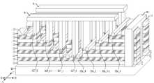
도 1a 및 도 1b는 종래기술에 따른 3차원 구조의 비휘발성 메모리 장치를 도시한 사시도이다.1A and 1B are perspective views illustrating a nonvolatile memory device having a three-dimensional structure according to the prior art.
도 1a에 도시된 바와 같이, 종래기술에 따른 3차원 구조의 비휘발성 메모리 장치는 제1방향(I-I')으로 평행하게 확장된 복수의 채널구조물(C), 채널구조물(C)의 측벽을 따라 적층된 복수의 메모리셀(MC) 및 제2방향(II-II')으로 배열된 메모리셀(MC)들의 게이트전극에 연결된 워드라인(WL)을 구비한다.As shown in FIG. 1A, a non-volatile memory device having a three-dimensional structure according to the prior art includes a plurality of channel structures C and sidewalls of the channel structures C extended in parallel in a first direction I-I '. And a word line WL connected to the gate electrodes of the memory cells MC stacked along the gate electrodes of the memory cells MC arranged in the second direction II-II '.
채널구조물(C)은 기판(10)상에 교대로 적층된 복수의 층간절연막(11) 및 복수의 채널막(12)을 포함하며, 채널구조물(C)의 측벽을 따라 복수의 메모리셀(MC)들이 적층된다. 메모리셀(MC)은 채널막(12)상에 차례로 적층된 메모리막과 게이트전극(14)을 포함한다. 이때, 메모리막은 채널막(12) 상에 터널절연막(13A), 전하트랩막(13B) 및 전하차단막(13C)이 순차적으로 적층된 적층막이다.The channel structure C includes a plurality of
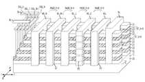
도 1b에 도시된 바와 같이, 종래기술에 따른 3차원 구조의 비휘발성 메모리 장치는 복수의 드레인선택라인(DSL_0~DSL_X), 드레인콘택플러그(DCT_0~DCT_X) 및 비트라인(BL)을 구비한다. 이하, 종래기술에 따른 드레인선택라인(DSL_0~DSL_X), 드레인콘택플러그(DCT_0~DCT_X) 및 비트라인(BL) 형성방법에 대해 설명한다.As illustrated in FIG. 1B, the nonvolatile memory device having a three-dimensional structure according to the related art includes a plurality of drain selection lines DSL_0 to DSL_X, drain contact plugs DCT_0 to DCT_X, and a bit line BL. Hereinafter, a method of forming the drain selection lines DSL_0 to DSL_X, the drain contact plugs DCT_0 to DCT_X, and the bit line BL according to the related art will be described.
먼저, 채널구조물(C)의 드레인선택트랜지스터영역을 계단형으로 식각하여 복수의 채널막(12)을 각각 노출시킨 후, 노출된 채널막(12)상에 게이트절연막(15)을 형성한다. 이어서, 게이트절연막(15) 상에 게이트전극용 도전막을 각각 형성하여 드레인선택트랜지스터를 형성한 후, 제2방향으로 배열되는 드레인선택트랜지스터를 연결시키면서, 제2방향으로 평행하게 확장되는 복수의 드레인선택라인(DSL_0~DSL_X)을 형성한다.First, the drain select transistor region of the channel structure C is etched stepwise to expose the plurality of
이로써, 복수의 채널막(12) 상에 평판형의 드레인선택트랜지스터가 각각 형성되며, 동일한 층의 채널막(12) 상에 형성되어 제2방향으로 배열되는 드레인선택 트랜지스터들이 드레인선택라인(DSL_0~DSL_X)에 의해 연결된다.As a result, planar drain select transistors are formed on the plurality of
이어서, 결과물의 전체 구조상에 절연막(미도시됨)을 형성한 후, 복수의 채널막(12) 표면을 각각 노출시키는 드레인 콘택홀을 형성한 후, 드레인 콘택홀 내에 도전막을 매립하여 복수의 채널막(12)에 각각 연결된 드레인콘택플러그(DCT_0~DCT_X)를 형성한다. 이어서, 제1방향으로 배열되는 드레인콘택플러그(DCT_0~DCT_X)들과 연결되면서, 제1방향으로 평행하게 확장되는 복수의 비트라인(BL)을 형성한다.Subsequently, after forming an insulating film (not shown) on the entire structure of the resultant, a drain contact hole for exposing the surfaces of the plurality of
그러나, 상술한 종래기술에 따르면 채널구조물(C)을 계단형으로 패터닝하여 복수의 채널막(12)을 노출시킨 후 노출된 채널막(12)마다 평판형의 드레인선택트랜지스터를 형성하기 때문에, 평판형의 드레인선택트랜지스터를 형성하기 위해 상당한 면적이 요구된다. 따라서, 채널막(12)의 적층 수를 증가시키더라도 그에 따라 드레인 선택 트랜지스터를 위한 요구 면적이 증가하기 때문에 메모리 장치의 집적도를 향상시키는데 한계가 있다. 뿐만 아니라, 평판형의 드레인 선택 트랜지스터를 형성하는 경우, 누설전류가 발생할 확률이 높기 때문에 메모리 장치의 특성이 저하된다.However, according to the above-described conventional technique, since the channel structure C is patterned stepwise to expose the plurality of
또한, 종래기술은 드레인선택트랜지스터의 게이트전극으로 드레인선택라인(DSL_0~DSL_X)을 사용하고, 게이트절연막(15)과의 접합특성을 고려하여 드레인선택라인(DSL_0~DSL_X)을 폴리실리콘막으로 형성한다. 여기서, 메모리 장치의 신호전달 특성을 향상시키기 위해서는 드레인선택라인(DSL_0~DSL_X)의 저항을 감소시켜야만 한다. 하지만, 폴리실리콘막으로 이루어진 드레인선택라인(DSL_0~DSL_X)은 저항을 감소시키는데 한계가 있다. 참고로, 드레인선택라인(DSL_0~DSL_X)의 저항을 감소시키기 위해 드레인선택라인(DSL_0~DSL_X)을 금속막 또는 금속실리사이드막과 같은 저저항 금속성막으로 형성하면, 드레인선택트랜지스터의 게이트절연막(15)과 금속성이 직접 맞닿는 문제가 발생하여 드레인선택트랜지스터의 오동작을 유발하는 문제점이 발생한다.
In the related art, the drain selection lines DSL_0 to DSL_X are used as the gate electrodes of the drain selection transistor, and the drain selection lines DSL_0 to DSL_X are formed of a polysilicon film in consideration of the bonding characteristics with the
본 발명은 상기한 종래기술의 문제점을 해결하기 위하여 제안된 것으로, 선택트랜지스터를 위한 요구 면적을 감소시킬 수 있는 3차원 구조의 비휘발성 메모리 장치 및 그 제조방법을 제공하는데 그 목적이 있다.SUMMARY OF THE INVENTION The present invention has been proposed to solve the above problems of the prior art, and an object thereof is to provide a three-dimensional nonvolatile memory device capable of reducing the area required for a selection transistor and a method of manufacturing the same.
또한, 본 발명은 누설전류 발생을 억제할 수 있는 선택트랜지스터를 구비한 3차원 구조의 비휘발성 메모리 장치 및 그 제조방법을 제공하는데 다른 목적이 있다.Another object of the present invention is to provide a three-dimensional nonvolatile memory device having a selection transistor capable of suppressing leakage current and a method of manufacturing the same.
또한, 본 발명은 선택라인의 저항을 감소시킴과 동시에 선택라인과 연결된 선택트랜지스터의 오동작을 방지할 수 있는 3차원 구조의 비휘발성 메모리 장치 및 그 제조방법을 제공하는데 또 다른 목적이 있다.
Another object of the present invention is to provide a non-volatile memory device having a three-dimensional structure and a method of manufacturing the same, which can reduce the resistance of the selection line and prevent the malfunction of the selection transistor connected to the selection line.
상기 목적을 달성하기 위한 일 측면에 따른 본 발명은 복수회 교번 적층된 채널막 및 층간절연막을 포함하는 채널구조물; 상기 채널구조물 양측에서 복수의 상기 채널막과 각각 연결된 채널콘택; 상기 채널콘택 상부를 가로지르고, 실리콘보다 낮은 저항을 갖는 저저항 물질을 포함하는 선택라인; 및 상기 선택라인에 매립되어 상기 채널콘택과 연결된 선택트랜지스터를 포함하는 3차원 구조의 비휘발성 메모리 장치를 제공한다.According to an aspect of the present invention, there is provided a channel structure including a channel layer and an interlayer insulating layer alternately stacked a plurality of times; Channel contacts connected to the channel layers on both sides of the channel structure; A selection line crossing the channel contact and including a low resistance material having a lower resistance than silicon; And a selection transistor embedded in the selection line and connected to the channel contact.
상기 선택트랜지스터는 게이트 올 어라운드 구조를 가질 수 있다. 구체적으로, 상기 선택 트랜지스터는 상기 채널콘택과 수직으로 연결된 필라형 채널; 상기 필라형 채널을 감싸는 게이트절연막; 상기 게이트절연막을 감싸고, 실리콘막을 포함하는 게이트전극; 및 상기 게이트전극을 감싸고, 금속성막을 포함하는 선택라인을 포함할 수 있다. 이때, 상기 금속성막은 금속막, 금속산화막, 금속질화막 및 금속실리사이드막으로 이루어진 그룹으로부터 선택된 어느 하나를 포함할 수 있다.The selection transistor may have a gate all around structure. Specifically, the selection transistor may include a pillar channel vertically connected to the channel contact; A gate insulating film surrounding the pillar channel; A gate electrode surrounding the gate insulating film and including a silicon film; And a selection line surrounding the gate electrode and including a metallic film. In this case, the metallic film may include any one selected from the group consisting of a metal film, a metal oxide film, a metal nitride film, and a metal silicide film.
상기 선택라인은 드레인선택라인을 포함할 수 있다.The selection line may include a drain selection line.
또한, 본 발명은 상기 선택라인 상부에 형성되어 상기 선택트랜지스터를 통해 상기 채널콘택과 연결되고, 상기 선택라인과 교차하는 비트라인을 더 포함할 수 있다. 이때, 상기 비트라인은 상기 채널구조물과 동일한 방향으로 연장된 구조를 가질 수 있다.The present invention may further include a bit line formed on the selection line and connected to the channel contact through the selection transistor and intersecting the selection line. In this case, the bit line may have a structure extending in the same direction as the channel structure.
상기 선택라인은 단일층으로 형성되어 상기 선택트랜지스터를 통해 복수의 상기 채널콘택과 각각 연결된 구조를 가질 수 있다.The selection line may be formed as a single layer and have a structure connected to each of the plurality of channel contacts through the selection transistor.
또한, 상기 선택라인은 복수 층으로 형성될 수도 있다. 일례로, 상기 선택라인은 복수의 상기 채널콘택 중 일부 채널콘택과 각각 연결된 1차 선택라인; 및 상기 1차 선택라인과 다른 층에서 상기 1차 선택라인과 엇갈리게 배열되어 복수의 상기 채널콘택 중 나머지 채널콘택과 각각 연결된 2차 선택라인을 포함할 수 있다. 또 다른 일례로, 상기 선택라인은 복수의 상기 채널콘택 중 적어도 두 개의 인접한 채널콘택과 연결된 1차 선택 라인; 및 상기 1차 선택라인과 다른 층에서 복수의 상기 채널콘택 중 적어도 두 개의 인접한 채널콘택과 연결되되, 상기 1차 선택라인과 일부 채널콘택을 공유하도록 형성된 2차 선택라인을 포함할 수 있다.
In addition, the selection line may be formed of a plurality of layers. For example, the selection line may include a first selection line connected to some channel contacts of the plurality of channel contacts; And a second selection line arranged alternately with the first selection line in a layer different from the first selection line and connected to the remaining channel contacts of the plurality of channel contacts, respectively. In another example, the selection line may include a first selection line connected to at least two adjacent channel contacts of the plurality of channel contacts; And a second selection line connected to at least two adjacent channel contacts of the plurality of channel contacts in a layer different from the first selection line, and configured to share some channel contacts with the first selection line.
상기 목적을 달성하기 위한 다른 일 측면에 따른 본 발명은 복수회 교번 적층된 채널막 및 층간절연막을 포함하는 채널구조물과 상기 채널구조물을 덮는 제1층간절연막을 형성하는 단계; 상기 제1층간절연막을 관통하여 상기 채널구조물 양측에서 복수의 상기 채널막과 각각 연결되는 채널콘택을 형성하는 단계; 및 상기 채널콘택 상부를 가로지르고, 실리콘보다 낮은 저항을 갖는 저저항 물질을 포함하는 선택라인과 상기 선택라인에 매립되어 상기 채널콘택과 연결된 선택트랜지스터를 형성하는 단계를 포함하는 3차원 구조의 비휘발성 메모리 장치 제조방법을 제공한다.According to another aspect of the present invention, there is provided a method including: forming a channel structure including a channel layer and an interlayer insulating layer alternately stacked a plurality of times and a first interlayer insulating layer covering the channel structure; Forming a channel contact penetrating through the first interlayer insulating film and connected to the plurality of channel films on both sides of the channel structure; And a selection line comprising a low resistance material having a lower resistance than silicon and crossing the upper portion of the channel contact and embedded in the selection line to form a selection transistor connected to the channel contact. A memory device manufacturing method is provided.
일례로, 상기 선택라인 및 상기 선택트랜지스터를 형성하는 단계는, 상기 채널콘택 상부를 가로지르고, 금속성막을 포함하는 선택라인을 형성하는 단계; 및 상기 선택라인에 매립되고, 상기 채널콘택과 연결된 게이트 올 어라운드 구조의 선택트랜지스터를 형성하는 단계를 포함할 수 있다.For example, the forming of the selection line and the selection transistor may include forming a selection line across the channel contact and including a metallic film; And forming a selection transistor having a gate all around structure embedded in the selection line and connected to the channel contact.
여기서, 본 발명은 상기 선택라인을 형성하기 이전에 상기 제1층간절연막 상에 제2층간절연막을 형성하는 단계; 상기 선택라인을 형성한 이후에 상기 제2층간절연막 상에 제3층간절연막을 형성하는 단계; 및 상기 선택트랜지스터를 형성한 이후에 상기 제3층간절연막 상에 상기 선택트랜지스터와 연결되고, 상기 선택라인과 교차하는 비트라인을 형성하는 단계를 더 포함할 수 있다.In an embodiment, the present invention provides a method for forming a semiconductor device, the method comprising: forming a second interlayer insulating film on the first interlayer insulating film before forming the selection line; Forming a third interlayer insulating film on the second interlayer insulating film after forming the selection line; And forming a bit line connected to the selection transistor on the third interlayer insulating layer and intersecting the selection line after the selection transistor is formed.
상기 선택라인을 형성하는 단계는 상기 제2층간절연막 상에 선택라인용 도전막을 형성하는 단계; 및 상기 채널콘택 상부를 덮도록 상기 선택라인용 도전막을 식각하는 단계를 포함할 수 있다.The forming of the selection line may include forming a conductive film for the selection line on the second interlayer insulating layer; And etching the conductive film for the selection line to cover the upper portion of the channel contact.
상기 선택트랜지스터를 형성하는 단계는, 상기 제3층간절연막 및 상기 선택라인을 식각하여 홀을 형성하는 단계; 상기 홀의 측벽에 실리콘막을 포함하는 게이트전극을 형성하는 단계; 상기 채널콘택이 노출되도록 상기 홀 저면 아래의 상기 제2층간절연막을 식각하여 상기 홀을 확장시키는 단계; 확장된 상기 홀의 측벽에 게이트절연막을 형성하는 단계; 및 나머지 상기 홀을 매립하는 필라형 채널을 형성하는 단계를 포함할 수 있다. 이때, 상기 홀의 외측벽을 상기 선택라인이 감싸도록 형성할 수 있다.The forming of the selection transistor may include forming a hole by etching the third interlayer insulating layer and the selection line; Forming a gate electrode including a silicon film on sidewalls of the hole; Etching the second interlayer dielectric under the hole to expose the channel contact to extend the hole; Forming a gate insulating film on sidewalls of the extended holes; And forming a pillar-shaped channel filling the remaining holes. In this case, the outer wall of the hole may be formed to surround the selection line.
또 다른 일례로, 상기 선택라인 및 상기 선택트랜지스터를 형성하는 단계는, 상기 제1층간절연막 상에 상기 채널콘택과 연결된 게이트 올 어라운드 구조의 선택트랜지스터를 형성하는 단계; 및 상기 제1층간절연막 상에 인접한 상기 선택트랜지스터를 연결하고, 금속성막을 포함하는 선택라인을 형성하는 단계를 포함할 수 있다.As another example, the forming of the selection line and the selection transistor may include forming a selection transistor having a gate all around structure connected to the channel contact on the first interlayer insulating layer; And connecting the selection transistors adjacent to the first interlayer insulating layer, and forming a selection line including a metallic layer.
여기서, 본 발명은 상기 선택라인 상부에 상기 선택라인과 교차하고, 상기 선택트랜지스터를 통해 상기 채널콘택과 연결되는 비트라인을 형성하는 단계를 더 포함할 수 있다.The present invention may further include forming a bit line intersecting the selection line on the selection line and connected to the channel contact through the selection transistor.
상기 선택트랜지스터를 형성하는 단계는, 상기 제1층간절연막을 일부 리세스하여 상기 제1층간절연막 위로 상기 채널콘택을 일부 돌출시키는 단계; 돌출된 상기 채널콘택을 감싸도록 게이트절연막을 형성하는 단계; 및 돌출된 상기 채널콘택의 측벽을 감싸도록 상기 게이트절연막 상에 실리콘막을 포함하는 게이트전극을 형성하는 단계를 포함할 수 있다.The forming of the selection transistor may include: partially recessing the first interlayer insulating layer to partially protrude the channel contact over the first interlayer insulating layer; Forming a gate insulating film to surround the protruding channel contact; And forming a gate electrode including a silicon layer on the gate insulating layer to surround sidewalls of the protruding channel contacts.
상기 선택라인을 형성하는 단계는, 상기 제1층간절연막 상에 선택라인용 도전막을 형성하는 단계; 게이트전극의 상부면보다 낮은 상부면을 갖도록 상기 선택라인용 도전막을 전면식각하는 단계; 및 상기 게이트전극을 감싸고, 인접한 상기 상기 게이트전극 사이를 연결하도록 상기 선택라인용 도전막을 패터닝하는 단계를 포함할 수 있다.The forming of the selection line may include forming a conductive film for the selection line on the first interlayer insulating layer; Etching the conductive film for the select line to have an upper surface lower than an upper surface of a gate electrode; And encapsulating the gate electrode and patterning the conductive layer for the selection line to connect the adjacent gate electrodes.
상기 선택라인은 드레인선택라인을 포함할 수 있고, 상기 금속성막은 금속막, 금속산화막, 금속질화막 및 금속실리사이드막으로 이루어진 그룹으로부터 선택된 어느 하나를 포함할 수 있다.The selection line may include a drain selection line, and the metallic layer may include any one selected from the group consisting of a metal layer, a metal oxide layer, a metal nitride layer, and a metal silicide layer.
상술한 과제 해결 수단을 바탕으로 하는 본 발명은, 선택트랜지스터가 게이트 올 어라운드 구조를 가짐으로써, 평판형의 선택트랜지스터에 비해 누설전류의 발생을 감소시킬 수 있는 효과가 있다. 아울러, 선택트랜지스터의 오프 특성을 개선할 수 있는 효과가 있다. 아울러, 선택트랜지스터를 위한 요구 면적을 감소시킬 수 있으며, 이를 통해 메모리 장치의 집적도를 증가시킬 수 있는 효과가 있다.The present invention based on the above-described problem solving means has an effect that the selection transistor has a gate all-around structure, which can reduce the generation of leakage current as compared with the planar selection transistor. In addition, there is an effect that can improve the off characteristics of the selection transistor. In addition, the area required for the selection transistor can be reduced, thereby increasing the density of the memory device.
또한, 본 발명은 복수의 선택라인 및 선택트랜지스터가 동일한 층에 배치됨으로써, 이들을 형성하기 위한 공정의 난이도를 감소시킬 수 있는 효과가 있다.In addition, the present invention has the effect of reducing the difficulty of the process for forming a plurality of select lines and select transistors are arranged in the same layer.
또한, 본 발명은 선택라인을 저저항 금속성막으로 형성함에 따라 선택라인의 신호전달 특성을 향상시킬 수 있는 효과가 있다.In addition, the present invention has the effect of improving the signal transmission characteristics of the selection line by forming the selection line with a low resistance metallic film.
또한, 본 발명은 필라형 채널을 감싸는 게이트절연막을 실리콘막으로 이루어진 게이트전극이 감싸고, 금속성막으로 이루어진 선택라인은 게이트전극을 감싸는 구조를 가짐으로써, 게이트절연막과 금속성막으로 이루어진 선택라인 간의 직접 접촉에 따른 선택트랜지스터의 오동작을 방지할 수 있는 효과가 있다.
In addition, the present invention has a structure in which a gate electrode made of a silicon film surrounds the gate insulating film surrounding the pillar-type channel, and the selection line made of the metallic film has a structure surrounding the gate electrode, thereby directly contacting the gate insulating film and the selection line made of the metal film. There is an effect that can prevent the malfunction of the selection transistor according to.
도 1a 및 도 1b는 종래기술에 따른 3차원 구조의 비휘발성 메모리 장치를 도시한 사시도.
도 2a는 본 발명의 일실시예에 따른 3차원 구조의 비휘발성 메모리 장치를 도시한 레이아웃.
도 2b는 본 발명의 일실시예에 따른 3차원 구조의 비휘발성 메모리 장치 셀 어레이 일부를 나타내는 회로도.
도 2c는 본 발명의 일실시예에 따른 3차원 구조의 비휘발성 메모리 장치를 도시한 사시도.
도 2d는 본 발명의 제1실시예에 따른 드레인선택라인 및 드레인선택트랜지스터를 구비한 3차원 구조의 비휘발성 메모리 장치를 도시한 단면도.
도 2e는 본 발명의 제2실시예에 따른 드레인선택라인 및 드레인선택트랜지스터를 구비한 3차원 구조의 비휘발성 메모리 장치를 도시한 단면도.
도 2f는 본 발명의 제3실시예에 따른 드레인선택라인 및 드레인선택트랜지스터를 구비한 3차원 구조의 비휘발성 메모리 장치를 도시한 단면도.
도 3a 내지 도 3f는 본 발명의 일실시예에 따른 3차원 구조의 비휘발성 메모리 장치 제조방법을 도시한 공정단면도.
도 4a 내지 도 4e는 본 발명의 다른 일실시예에 따른 3차원 구조의 비휘발성 메모리 장치 제조방법을 도시한 공정단면도.1A and 1B are perspective views illustrating a nonvolatile memory device having a three-dimensional structure according to the related art.
FIG. 2A is a layout illustrating a nonvolatile memory device having a three-dimensional structure according to an embodiment of the present invention. FIG.
FIG. 2B is a circuit diagram illustrating a portion of a nonvolatile memory device cell array having a three dimensional structure according to an embodiment of the present invention. FIG.
2C is a perspective view illustrating a nonvolatile memory device having a three-dimensional structure according to an embodiment of the present invention.
FIG. 2D is a cross-sectional view of a three-dimensional nonvolatile memory device having a drain select line and a drain select transistor according to a first embodiment of the present invention; FIG.
FIG. 2E is a cross-sectional view of a three-dimensional nonvolatile memory device having a drain select line and a drain select transistor according to a second embodiment of the present invention; FIG.
FIG. 2F is a cross-sectional view of a three-dimensional nonvolatile memory device having a drain select line and a drain select transistor according to a third embodiment of the present invention; FIG.
3A through 3F are cross-sectional views illustrating a method of manufacturing a nonvolatile memory device having a three-dimensional structure, according to an embodiment of the present invention.
4A to 4E are cross-sectional views illustrating a method of manufacturing a nonvolatile memory device having a three-dimensional structure according to another embodiment of the present invention.
이하 본 발명이 속하는 기술분야에서 통상의 지식을 가진자가 본 발명의 기술적 사상을 용이하게 실시할 수 있을 정도로 상세히 설명하기 위하여, 본 발명의 가장 바람직한 실시예를 첨부도면을 참조하여 설명하기로 한다.DETAILED DESCRIPTION OF THE PREFERRED EMBODIMENT Hereinafter, preferred embodiments of the present invention will be described in detail with reference to the accompanying drawings, in order to facilitate a person skilled in the art to easily carry out the technical idea of the present invention.
후술할 본 발명은 선택트랜지스터를 위한 요구 면적을 감소시키고, 선택트랜지스터의 누설전류 발생을 억제하며, 선택라인의 저항을 감소시킴과 동시에 선택라인과 연결된 선택트랜지스터의 오동작을 방지할 수 있는 3차원 구조의 비휘발성 메모리 장치 및 그 제조방법을 제공한다.The present invention, which will be described later, reduces a required area for a selection transistor, suppresses leakage current of the selection transistor, reduces resistance of the selection line, and simultaneously prevents malfunction of the selection transistor connected to the selection line. A nonvolatile memory device and a method of manufacturing the same are provided.
이를 위해, 본 발명은 선택트랜지스터를 위한 요구 면적 감소 및 선택트랜지스터의 누설전류 발생을 억제하기 위해 선택트랜지스터가 게이트 올 어라운드(Gate All Around;GAA)를 갖도록 형성하는 것을 특징으로 한다. 또한, 본 발명은 선택라인의 저항을 감소시키기 위해 선택라인은 저저항 금속성막으로 형성하는 것을 다른 특징으로 한다. 또한, 본 발명은 선택라인을 저저항 금속성막으로 형성함에 따라 유발되는 선택트랜지스터의 오동작을 방지하기 위해 선택트랜지스터의 게이트절연막과 선택라인 사이에 실리콘막으로 이루어진 게이트전극을 삽입하여 선택라인과 게이트절연막 사이의 직접 접촉을 방지하는 것을 또 다른 특징으로 한다.To this end, the present invention is characterized in that the selection transistor is formed to have a gate all around (GAA) in order to reduce the required area for the selection transistor and to suppress the occurrence of leakage current of the selection transistor. In addition, the present invention is characterized in that the selection line is formed of a low resistance metallic film in order to reduce the resistance of the selection line. In addition, the present invention inserts a gate electrode made of a silicon film between the gate insulating film and the selection line of the selection transistor in order to prevent the malfunction of the selection transistor caused by forming the select line as a low-resistance metallic film, the selection line and the gate insulating film Another feature is to prevent direct contact therebetween.
이하, 본 발명의 실시예들을 통해 상술한 본 발명의 기술적 특징에 대하여 보다 구체적으로 설명한다.Hereinafter, the technical features of the present invention described above will be described in more detail with reference to the embodiments of the present invention.
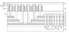
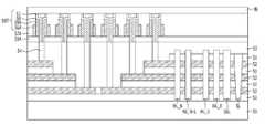
도 2a는 본 발명의 일실시예에 따른 3차원 구조의 비휘발성 메모리 장치를 도시한 레이아웃이다.2A is a layout illustrating a nonvolatile memory device having a three-dimensional structure according to an embodiment of the present invention.
도 2a에 도시된 바와 같이, 기판상에는 제1방향(I-I')으로 평행하게 확장되는 복수의 비트라인(BL)이 구비되고, 상기 제1방향과 교차하는 제2방향(II-II')으로 평행하게 확장되는 다수의 워드라인(WL)이 구비된다.As shown in FIG. 2A, a plurality of bit lines BL extending in parallel in a first direction I-I 'are provided on a substrate, and a second direction II-II' intersecting the first direction is provided. ) Are provided with a plurality of word lines WL extending in parallel.
비트라인(BL)은 데이터를 입출력하기 위한 것이다. 본 도면에는 나타나지 않았으나, 하나의 비트라인(BL)에 대해 복수의 스트링(ST_0~ST_X)이 적층되어 연결된다. 또한, 복수의 비트라인(BL)에 연결된 복수의 스트링(ST)들은 소스라인(SL)에 병렬 연결되어 메모리 블록(MB)을 구성한다.The bit line BL is for inputting and outputting data. Although not shown in the drawing, a plurality of strings ST_0 to ST_X are stacked and connected to one bit line BL. In addition, the plurality of strings ST connected to the plurality of bit lines BL are connected to the source line SL in parallel to constitute a memory block MB.
워드라인(WL)은 메모리셀을 선택하여 활성화하기 위한 것이다. 본 도면에는 나타나지 않았으나, 하나의 워드라인(WL)에 대해 복수의 페이지(PAGE_0~PAGE_X)가 적층되어 연결된다. 또한, 채널 콘택을 통해 복수의 채널막과 각각 연결된 드레인선택라인(DSL_0~DSL_N)에 의해 원하는 페이지(PAGE)가 선택된다.The word line WL is for selecting and activating a memory cell. Although not shown in the drawing, a plurality of pages PAGE_0 to PAGE_X are stacked and connected to one word line WL. In addition, a desired page PAGE is selected by the drain selection lines DSL_0 to DSL_N respectively connected to the plurality of channel layers through the channel contact.
여기서, 복수의 비트라인(BL)들은 페이지 버퍼(PB)에 연결되며, 페이지 버퍼(PB)는 입력된 어드레스를 디코딩하여 해당 비트라인(BL)을 제어한다. 또한, 복수의 워드라인(WL)들은 X-디코더(X-decoder)로 연결되며, X-디코더는 입력된 어드레스를 디코딩하여 해당 워드라인(WL)을 제어한다.Here, the plurality of bit lines BL are connected to the page buffer PB, and the page buffer PB controls the corresponding bit line BL by decoding the input address. In addition, the plurality of word lines WL are connected to an X-decoder, and the X-decoder decodes the input address to control the corresponding word line WL.
또한, 기판상에는 제2방향으로 평행하게 확장되는 복수의 소스선택라인(SSL)이 구비되며, 소스선택라인(SSL) 사이의 접합 영역에는 소스라인(SL)이 구비된다.In addition, a plurality of source selection lines SSL extending in parallel in the second direction are provided on the substrate, and a source line SL is provided in the junction region between the source selection lines SSL.
또한, 기판상에는 제2방향으로 평행하게 확장되는 복수의 드레인선택라인(DSL_0~DSL_N)이 구비된다. 본 발명에 따르면, 복수층의 채널막과 각각 연결되는 복수의 채널 콘택이 구비되고, 채널 콘택에 의해 복수층의 채널막과 드레인선택라인(DSL_0~DSL_N)이 연결된다.In addition, a plurality of drain selection lines DSL_0 to DSL_N extend in parallel in the second direction on the substrate. According to the present invention, a plurality of channel contacts respectively connected to a plurality of channel films are provided, and the plurality of channel films and the drain selection lines DSL_0 to DSL_N are connected by the channel contacts.
본 도면에서는 각각의 채널막마다 각각 복수의 드레인선택라인(DSL_0~DSL_N)이 구비되는 경우에 대해 도시되어 있는데, 이는 일실시예에 불과하며 본 발명이 이에 한정되는 것은 아니다. 이 밖에도, 하나의 드레인선택라인(DSL)이 복수의 채널 콘택과 연결되는것 또한 가능하다. 즉, 하나의 드레인선택라인(DSL)이 복수의 채널 콘택을 통해 복수층의 채널막과 연결되는 것 또한 가능하다.In the drawing, a plurality of drain selection lines DSL_0 to DSL_N are provided for each channel film, but this is only an example and the present invention is not limited thereto. In addition, it is also possible that one drain select line DSL is connected to a plurality of channel contacts. That is, it is also possible for one drain selection line DSL to be connected to a plurality of channel layers through a plurality of channel contacts.
여기서, 복수의 드레인선택라인(DSL_0~DSL_N)들은 Z-디코더(Z-DECODER)로 연결되며, Z-디코더는 입력된 어드레스를 디코딩하여 해당 드레인선택라인(DSL)을 제어한다.Here, the plurality of drain selection lines DSL_0 to DSL_N are connected to the Z-decoder Z-DECODER, and the Z-decoder decodes the input address to control the corresponding drain selection line DSL.
도 2b는 본 발명의 일실시예에 따른 3차원 구조의 비휘발성 메모리 장치 셀 어레이 일부를 나타내는 회로도이다. 단, 설명의 편의를 위하여, 하나의 비트라인(BL)에 연결된 복수의 스트링(ST)을 중심으로 도시하였다.FIG. 2B is a circuit diagram illustrating a portion of a nonvolatile memory device cell array having a three-dimensional structure according to an embodiment of the present invention. However, for convenience of description, the plurality of strings ST connected to one bit line BL are illustrated.
도 2b에 도시된 바와 같이, 하나의 비트라인(BL)에 대하여 복수의 스트링(ST_0~ST_X)이 연결된다. 또한, 복수의 스트링(ST_0~ST_X)들은 각각 복수의 채널 콘택에 의해 복수의 드레인선택라인(DSL_0~DSL_N)과 연결된다.As illustrated in FIG. 2B, a plurality of strings ST_0 to ST_X are connected to one bit line BL. In addition, the strings ST_0 to ST_X are connected to the drain selection lines DSL_0 to DSL_N by a plurality of channel contacts, respectively.
따라서, 읽기/쓰기 동작시 원하는 페이지(PAGE)에 연결된 드레인선택라인(DSL)은 활성화하고, 그 외의 드레인선택라인(DSL)은 비활성화함으로써, 원하는 페이지(PAGE)를 선택할 수 있다.Accordingly, the desired page PAGE may be selected by activating the drain select line DSL connected to the desired page PAGE and deactivating the other drain select line DSL during the read / write operation.
메모리셀(MC)은 채널 구조물(C)을 중심으로 양 측벽에 게이트전극을 구비하는 더블 게이트(Dual Gate) 구조를 갖는다.The memory cell MC has a double gate structure having gate electrodes on both sidewalls of the channel structure C. Referring to FIG.
도 2c는 본 발명의 일실시예에 따른 3차원 구조의 비휘발성 메모리 장치를 도시한 사시도이다.FIG. 2C is a perspective view illustrating a nonvolatile memory device having a three-dimensional structure according to an embodiment of the present invention. FIG.
도 2c에 도시된 바와 같이, 제1방향(I-I')으로 평행하게 확장되는 복수의 채널구조물(C) 및 채널구조물(C)의 측벽을 따라 적층된 복수의 메모리셀(MC)을 구비하며, 제1방향(I-I')으로 평행하게 확장되는 복수의 비트라인(BL)을 구비한다.As shown in FIG. 2C, a plurality of channel structures C extending in parallel in the first direction I-I 'and a plurality of memory cells MC stacked along sidewalls of the channel structures C are provided. And a plurality of bit lines BL extending in parallel in the first direction I-I '.
여기서, 채널구조물(C)은 기판(20)상에 교대로 적층된 복수의 채널막(22) 및 층간절연막(21)으로 이루어지며, 적층된 채널막(22)의 갯수에 따라 비트라인(BL)을 공유하는 스트링(ST)의 갯수가 결정된다.Here, the channel structure C is composed of a plurality of
채널구조물(C)의 일측 끝단은 복수의 채널막(22)과 각각 연결되는 복수의 채널 콘택을 형성하기 위해 복수의 채널막(22)이 각각 노출되도록 패터닝 될 수 있다. 본 도면에서는 일 예로서, 채널구조물(C)의 일측 끝단이 계단형으로 패터닝된 경우에 대해 도시하고 있다.One end of the channel structure C may be patterned such that the plurality of channel layers 22 are exposed to form a plurality of channel contacts respectively connected to the plurality of channel layers 22. In this drawing, as an example, one end of the channel structure C is patterned in a stepped manner.
복수의 메모리셀(MC)들은 워드라인(WL_0~WL_N)과 채널막(22) 사이에 개재되고, 터널절연막, 전하트랩막 및 전하차단막이 적층된 구조의 메모리막(23)을 포함하며, 채널구조물(C)의 측벽을 따라 적층되어 제1방향 및 제2방향으로 배열된다. 여기서, 제1방향으로 배열되어 채널막(22)을 공유하는 동일한 층의 복수의 메모리셀(MC)들은 소스 선택 트랜지스터와 드레인 선택 트랜지스터 사이에 직렬 연결되어 스트링(ST) 구조를 형성하게 된다.The plurality of memory cells MC are interposed between the word lines WL_0 to WL_N and the
또한, 본 발명의 일실시예에 따른 3차원 구조의 비휘발성 메모리 장치는 제2방향(II-II')으로 평행하게 확장되는 복수의 워드라인(WL_0~WL_N), 소스선택라인(SSL) 및 소스라인(SL)을 구비한다.In addition, the nonvolatile memory device having a three-dimensional structure according to an embodiment of the present invention includes a plurality of word lines WL_0 to WL_N, a source selection line SSL, and a plurality of parallel lines extending in a second direction II-II '. The source line SL is provided.
워드라인(WL)을 공유하는 복수의 메모리셀(MC)들 중에서도 동일한 층에 형성된 메모리셀(MC)들은 하나의 페이지(PAGE)를 구성하게 된다. 즉, 하나의 워드라인(WL)은 복수의 페이지(PAGE_0~PAGE_X)에 연결되며, 읽기/쓰기 동작시, 드레인선택라인(DSL_0~DSL_N)의 온/오프에 의해 원하는 페이지(PAGE)를 선택하게 된다.Among the plurality of memory cells MC sharing the word line WL, the memory cells MC formed in the same layer form one page PAGE. That is, one word line WL is connected to a plurality of pages PAGE_0 to PAGE_X, and in the read / write operation, the desired page PAGE is selected by turning on / off the drain selection lines DSL_0 to DSL_N. do.
물론, 동일한 층에 형성된 메모리셀(MC)일지라도, 연결된 비트라인에 따라 페이지(PAGE)가 구분될 수 있으며, 이븐 비트라인(even BL)에 연결된 페이지(PAGE)는 이븐 페이지(even PAGE)로 동작하고, 오드 비트라인(odd BL)에 연결된 페이지(PAGE)는 오드 페이지(odd PAGE)로 동작할 수 있다. 단, 본 명세서에서는 설명의 편의를 위하여 이븐 페이지(even PAGE)와 오드 페이지(odd PAGE)를 구분하여 도시하지는 않았다.Of course, even in the memory cell MC formed on the same layer, the page PAGE may be divided according to the connected bit line, and the page PAGE connected to the even bit line is operated as an even page. In addition, the page PAGE connected to the odd bit line odd BL may operate as an odd page. However, in the present specification, an even page and an odd page are not illustrated separately for convenience of description.
소스선택라인(SSL)은 메모리셀(MC) 및 워드라인(WL_0~WL_N) 형성시 함께 형성될 수 있다. 물론, 소스선택라인(SSL)은 워드라인(WL_0~WL_N)과 채널막(22) 사이에 게이트절연막(24)이 개재된다.The source selection line SSL may be formed together when the memory cell MC and the word lines WL_0 to WL_N are formed. Of course, the gate selection layer 24 is interposed between the word lines WL_0 to WL_N and the
소스라인(SL)은 소스선택라인(SSL)들 사이의 소스라인 예정 영역을 식각하여 트렌치를 형성한 후, 트렌치 내에 도전막을 매립하여 형성될 수 있다.The source line SL may be formed by etching a source line predetermined region between the source selection lines SSL to form a trench, and then filling a conductive layer in the trench.
또한, 본 발명의 일실시예에 따른 3차원 구조의 비휘발성 메모리 장치는 제2방향(II-II')으로 평행하게 확장되는 복수의 드레인선택라인(DSL_0~DSL_N)을 구비한다.In addition, the nonvolatile memory device having a three-dimensional structure according to an embodiment of the present invention includes a plurality of drain selection lines DSL_0 to DSL_N extending in parallel in the second direction II-II '.
복수의 드레인선택라인(DSL_0~DSL_N)은 채널 콘택을 통해 복수의 채널막으로 연결된다. 특히, 제2방향(II-II')으로 배열된 드레인선택라인(DSL_0~DSL_N)내에 게이트 올 어라운드(Gate All Around;GAA) 구조의 드레인 선택 트랜지스터가 매립되어 채널 콘택과 연결된다. 이와 같이, 게이트 올 어라운드 구조의 드레인 선택 트랜지스터를 형성함으로써, 종래의 평판형 구조의 드레인 선택 트랜지스터를 형성하는 경우에 비해 메모리 장치의 집적도를 향상시킬 수 있다.The plurality of drain selection lines DSL_0 to DSL_N are connected to the plurality of channel films through channel contacts. In particular, a drain select transistor having a gate all around (GAA) structure is buried in the drain select lines DSL_0 to DSL_N arranged in the second direction II-II 'to be connected to the channel contact. As described above, by forming the drain select transistor having the gate all around structure, the degree of integration of the memory device can be improved as compared with the case of forming the drain select transistor having the conventional planar structure.
본 도면에서는 복수의 드레인선택라인(DSL_0~DSL_N)이 단일층으로 형성되어 복수의 채널막으로 각각 연결되는 경우에 대해 도시되고 있으나, 이밖에도 복수의 드레인선택라인(DSL_0~DSL_N)이 복수층으로 형성되거나, 하나의 드레인선택라인(DSL)이 복수의 채널막과 연결되는 것 또한 가능하다.
In the drawing, a plurality of drain selection lines DSL_0 to DSL_N are formed in a single layer and connected to a plurality of channel films, respectively. In addition, a plurality of drain selection lines DSL_0 to DSL_N are formed in a plurality of layers. Alternatively, one drain select line DSL may be connected to the plurality of channel layers.
이하에서는 도 2a 내지 도 2c에서 상술한 내용을 바탕으로 본 발명의 드레인선택라인 및 드레인선택트랜지터에 대하여 도 2d 내지 도 2f를 참조하여 구체적으로 설명한다. 여기서, 도 2d 내지 도 2f는 도 2c에 도시된 제1방향(I-I') 단면으로 설명의 편의를 위해 드레인선택라인 및 드레인선택트랜지스터를 중심으로 도시하였으며, 메모리 셀등은 간략히 도시하였다.
Hereinafter, the drain selection line and the drain selection transistor of the present invention will be described in detail with reference to FIGS. 2D to 2F based on the above description with reference to FIGS. 2A to 2C. 2D to 2F are cross-sectional views of the drain selection line and the drain selection transistor in the first direction (I-I ') shown in FIG. 2C for convenience of explanation, and the memory cells and the like are briefly shown.
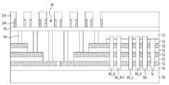
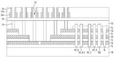
도 2d는 본 발명의 제1실시예에 따른 드레인선택라인 및 드레인선택트랜지스터를 구비한 3차원 구조의 비휘발성 메모리 장치를 도시한 단면도이다.FIG. 2D is a cross-sectional view illustrating a three-dimensional nonvolatile memory device having a drain select line and a drain select transistor according to a first embodiment of the present invention.
도 2d에 도시된 바와 같이, 본 발명의 제1실시예에 따른 메모리 장치는 기판(30)상에 복수회 교번 적층된 채널막(32) 및 층간절연막(31)을 포함한 복수의 채널구조물(C), 기판(30) 상에 형성되어 복수의 채널구조물(C)을 덮는 제1층간절연막(33), 제1층간절연막(33)을 관통하여 복수의 채널구조물(C) 양측에서 복수의 채널막(32)과 각각 연결된 복수의 채널콘택(34), 복수의 채널콘택(34) 상부를 가로지르고 저저항 물질 예컨대, 금속성막을 포함하는 드레인선택라인(36), 드레인선택라인(36)을 관통하여 채널콘택(34)과 연결되고, 게이트 올 어라운드 구조를 갖는 드레인선택트랜지스터(DST)를 포함한다. 여기서, 저저항 물질 예컨대, 금속성막은 금속막, 금속산화막, 금속질화막 및 금속실리사이드막으로 이루어진 그룹으로부터 선택된 어느 하나 또는 이들이 적층된 적층막을 포함한다.As shown in FIG. 2D, the memory device according to the first embodiment of the present invention includes a plurality of channel structures C including a
또한, 제1층간절연막(33) 상에 형성되어 복수의 드레인선택라인(36)과 드레인선택트랜지스터(DST)를 덮는 제2층간절연막(35) 및 드레인선택라인(36) 상부 즉, 제2층간절연막(35) 상에 형성되어 드레인선택라인(36)과 교차하고, 드레인선택트랜지스터(DST)와 연결된 비트라인(BL)을 더 포함한다.In addition, an upper portion of the second
게이트 올 어라운드 구조를 갖는 드레인선택트랜지스터(DST)는 채널콘택(34)에 수직으로 연결된 필라형(pillar type) 채널(39), 필라형 채널(39)을 감싸는 게이트절연막(38), 게이트절연막(38)을 감싸는 게이트전극(37) 및 게이트전극을 감싸는 드레인선택라인(36)을 포함한다. 이때, 게이트전극(37)은 금속성막으로 이루어진 드레인선택라인(36)과 게이트절연막(38)이 직접 접하는 것을 방지하고, 이들간 접촉특성을 양호하게 하기 위해 실리콘막으로 형성하는 것이 바람직하다. 예컨대, 실리콘막으로는 폴리실리콘막을 사용할 수 있다.A drain select transistor (DST) having a gate all around structure includes a
여기서, 금속성막을 포함하는 드레인선택라인(36)은 배선으로 작용함과 동시에 게이트전극(37)과 접하는 영역에서 드레인선택트랜지스터(DST)의 또 다른 게이트전극으로 작용한다. 이때, 금속성막은 실리콘막보다 저항이 낮기 때문에 드레인선택라인(36)으로 인해 드레인선택트랜지스터(DST)의 게이트전극(37)의 저항특성을 개선할 수 있으며, 결과적으로 드레인선택트랜지스터(DST)의 동작특성을 개선할 수 있다.Here, the
드레인선택라인(36)은 드레인선택트랜지스터(DST) 게이트전극(37)을 감싸고, 제2방향으로 배치된 게이트전극(37) 사이를 연결하는 구조를 갖는다. 그리고, 드레인선택라인(36)은 채널구조물(C)과 교차하는 방향으로 연장된 구조를 갖는다.The drain
상술한 구조를 갖는 3차원 구조의 비휘발성 메모리 장치는 드레인선택트랜지스터(DST)가 게이트 올 어라운드 구조를 가짐으로써, 종래의 평판형의 드레인선택 트랜지스터에 비해 누설전류의 발생을 감소시킬 수 있으며, 드레인선택트랜지스터(DST)의 오프 특성을 개선할 수 있다. 아울러, 드레인선택트랜지스터(DST)를 위한 요구 면적을 감소시킬 수 있으며, 이를 통해 메모리 장치의 집적도를 증가시킬 수 있다. 또한, 복수의 드레인선택라인(36) 및 드레인선택트랜지스터가 동일한 층에 배치됨으로써, 이들을 형성하기 위한 공정의 난이도를 감소시킬 수 있다. 또한, 드레인선택라인(36)을 저저항 금속성막으로 형성함에 따라 드레인선택라인(36)의 신호전달 특성을 향상시킬 수 있다. 또한, 필라형 채널(39)을 감싸는 게이트절연막(38)을 실리콘막으로 이루어진 게이트전극(38)이 감싸고, 금속성막으로 이루어진 드레인선택라인(36)은 게이트전극(38)을 감싸는 구조를 가짐으로써, 게이트절연막(38)과 드레인선택라인(36) 간의 직접 접촉에 따른 드레인선택트랜지스터의 오동작을 방지할 수 있다.
In the three-dimensional nonvolatile memory device having the above-described structure, since the drain select transistor DST has a gate all-around structure, it is possible to reduce the generation of leakage current as compared to the conventional flat drain select transistor, The off characteristic of the selection transistor DST may be improved. In addition, the required area for the drain select transistor DST may be reduced, thereby increasing the degree of integration of the memory device. In addition, since the plurality of
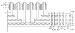
도 2e는 본 발명의 제2실시예에 따른 드레인선택라인 및 드레인선택트랜지스터를 구비한 3차원 구조의 비휘발성 메모리 장치를 도시한 단면도이다. 이하에서는, 설명의 편의를 위하여 본 발명의 제1실시예와 동일한 구성에 대해 동일한 도면부호를 사용하기로 한다.FIG. 2E is a cross-sectional view illustrating a nonvolatile memory device having a three-dimensional structure including a drain select line and a drain select transistor according to a second embodiment of the present invention. Hereinafter, for the convenience of description, the same reference numerals will be used for the same configuration as the first embodiment of the present invention.
도 2e에 도시된 바와 같이, 본 발명의 제2실시예에 따른 메모리 장치는 기판(30)상에 복수회 교번 적층된 채널막(32) 및 층간절연막(31)을 포함한 복수의 채널구조물(C), 기판(30) 상에 형성되어 복수의 채널구조물(C)을 덮는 제1층간절연막(33), 제1층간절연막(33)을 관통하여 복수의 채널구조물(C) 양측에서 복수의 채널막(32)과 각각 연결된 복수의 채널콘택(34), 복수의 채널콘택(34) 상부를 가로지르고 금속성막으로 이루어진 1차 및 2차 드레인선택라인(36, 41), 1차 드레인선택라인(36) 또는 2차 드레인선택라인(41)을 관통하여 채널콘택(34)과 연결되고, 게이트 올 어라운드 구조를 갖는 드레인선택트랜지스터(DST)를 포함한다. 또한, 1차 및 2차 드레인선택라인(36, 41) 상부에 형성되어 이들과 교차하고, 드레인선택트랜지스터(DST)와 연결된 비트라인(BL)을 더 포함한다.As shown in FIG. 2E, the memory device according to the second embodiment of the present invention includes a plurality of channel structures C including a
여기서, 1차 및 2차 드레인선택라인(36, 41)의 배치관계를 구체적으로 살펴보면, 제1층간절연막(35) 상에 형성되어 드레인선택트랜지스터(DST)를 통해 복수의 채널콘택(34) 중 일부 채널콘택(34)과 연결된 1차 드레인선택라인(36), 1차 드레인선택라인(36)을 덮는 제2층간절연막(35), 제2층간절연막(35) 상에 형성되어 드레인선택트랜지스터(DST)를 통해 복수의 채널콘택(34) 중 나머지 채널콘택(34)과 연결되고, 1차 드레인선택라인(36)과 엇갈리게 배치된 2차 드레인선택라인(41) 및 2차 드레인선택라인(41)을 덮는 제3층간절연막(40)을 포함한다.Herein, the arrangement relationship between the primary and secondary
게이트 올 어라운드 구조를 갖는 드레인선택트랜지스터(DST)는 채널콘택(34)에 수직으로 연결된 필라형(pillar type) 채널(39), 필라형 채널(39)을 감싸는 게이트절연막(38), 게이트절연막(38)을 감싸는 게이트전극(37) 및 게이트전극을 감싸는 1차 및 2차 드레인선택라인(36, 41)을 포함한다. 이때, 게이트전극(37)은 금속성막으로 이루어진 1차 및 2차 드레인선택라인(36, 41)과 게이트절연막(38)이 직접 접하는 것을 방지하고, 이들간 접촉특성을 양호하게 하기 위해 실리콘막으로 형성하는 것이 바람직하다. 예컨대, 실리콘막으로는 폴리실리콘막을 사용할 수 있다.A drain select transistor (DST) having a gate all around structure includes a
여기서, 금속성막을 포함하는 1차 및 2차 드레인선택라인(36, 41)은 배선으로 작용함과 동시에 게이트전극(37)과 접하는 영역에서 드레인선택트랜지스터(DST)의 또 다른 게이트전극으로 작용한다. 이때, 금속성막은 실리콘막보다 저항이 낮기 때문에 1차 및 2차 드레인선택라인(36, 41)으로 인해 드레인선택트랜지스터(DST)의 게이트전극(37)의 저항특성을 개선할 수 있으며, 결과적으로 드레인선택트랜지스터(DST)의 동작특성을 개선할 수 있다.Here, the primary and secondary
1차 및 2차 드레인선택라인(36, 41)은 드레인선택트랜지스터(DST) 게이트전극(37)을 감싸고, 제2방향으로 배치된 게이트전극(37) 사이를 연결하는 구조를 갖는다. 그리고, 1차 및 2차 드레인선택라인(36, 41)은 채널구조물(C)과 교차하는 방향으로 연장된 구조를 갖는다.The primary and secondary drain
상술한 구조를 갖는 본 발명의 제2실시예에 따른 메모리 장치는 본 발명의 제1실시예에 따른 메모리 장치가 구현하는 효과를 구현함과 동시에 1차 드레인선택라인(36)과 2차 드레인선택라인(41)이 서로 엇갈리게 배치됨과 동시에 서로 다른 층에 위치함에 따라 각각의 층에 형성된 드레인선택라인 사이의 간격을 보다 용이하게 확보할 수 있으며, 이를 통해 공정난이도를 감소시킬 수 있다. 아울러, 본 발명의 제1실시예보다 드레인선택라인의 형성을 위해 요구되는 면적을 감소시킬 수 있는 장점이 있다.The memory device according to the second embodiment of the present invention having the above-described structure realizes the effect realized by the memory device according to the first embodiment of the present invention and at the same time, the primary
참고로, 본 발명의 제2실시예에 따른 메모리 장치는 두 층으로 드레인선택라인이 형성되는 경우에 대해 도시하고 있으나, 이는 설명의 편의를 위한 것일 뿐이며, 드레인선택라인이 형성될 영역 및 메모리 장치의 집적도를 고려하여 드레인선택라인의 층수를 결정할 수 있다.
For reference, the memory device according to the second embodiment of the present invention is illustrated in the case where the drain selection line is formed of two layers, but this is only for convenience of description, and the region and the memory device in which the drain selection line is to be formed. The number of layers of the drain select line can be determined in consideration of the degree of integration.
도 2f는 본 발명의 제3실시예에 따른 드레인선택라인 및 드레인선택트랜지스터를 구비한 3차원 구조의 비휘발성 메모리 장치를 도시한 단면도이다. 이하에서는, 설명의 편의를 위하여 본 발명의 제1 및 제2실시예와 동일한 구성에 대해 동일한 도면부호를 사용하기로 한다.FIG. 2F is a cross-sectional view illustrating a three-dimensional nonvolatile memory device having a drain select line and a drain select transistor according to a third embodiment of the present invention. Hereinafter, for the convenience of description, the same reference numerals will be used for the same configurations as the first and second embodiments of the present invention.
도 2f에 도시된 바와 같이, 본 발명의 제3실시예에 따른 메모리 장치는 기판(30)상에 복수회 교번 적층된 채널막(32) 및 층간절연막(31)을 포함한 복수의 채널구조물(C), 기판(30) 상에 형성되어 복수의 채널구조물(C)을 덮는 제1층간절연막(33), 제1층간절연막(33)을 관통하여 복수의 채널구조물(C) 양측에서 복수의 채널막(32)과 각각 연결된 복수의 채널콘택(34), 복수의 채널콘택(34) 상부를 가로지르고 금속성막으로 이루어진 1차 및 2차 드레인선택라인(42, 43), 1차 드레인선택라인(42) 또는(및) 2차 드레인선택라인(43)을 관통하여 채널콘택(34)과 연결되고, 게이트 올 어라운드 구조를 갖는 드레인선택트랜지스터(DST)를 포함한다. 또한, 1차 및 2차 드레인선택라인(42, 43) 상부에 형성되어 이들과 교차하고, 드레인선택트랜지스터(DST)와 연결된 비트라인(BL)을 더 포함한다.As shown in FIG. 2F, a memory device according to a third embodiment of the present invention includes a plurality of channel structures C including a
여기서, 1차 및 2차 드레인선택라인(42, 43)의 배치관계를 구체적으로 살펴보면, 제1층간절연막(35) 상에 형성되어 드레인선택트랜지스터(DST)를 통해 복수의 채널콘택(34) 중 적어도 두 개의 인접한 채널콘택(34)과 연결된 1차 드레인선택라인(42), 1차 드레인선택라인(42)을 덮는 제2층간절연막(35), 제2층간절연막(35) 상에 형성되어 드레인선택트랜지스터(DST)를 통해 복수의 채널콘택(34) 중 적어도 구 개의 인접한 채널콘택(34)과 연결된 2차 드레인선택라인(43), 2차 드레인선택라인(43)을 덮는 제3층간절연막(40)을 포함한다. 즉, 1차 드레인선택라인(42) 및 2차 드레인선택라인(43)은 각각 적어도 2개의 채널콘택(34)과 연결되되, 일부 채널콘택(34)을 공유하도록 오버랩된 구조를 갖는다.Herein, the arrangement relationship between the primary and secondary
보다 구체적으로, 1차 드레인선택라인(42)과 2차 드레인선택라인(43)이 각각 2개의 채널콘택(34)과 연결되되, 상호 엇갈리게 배열된다. 예를들어, 1차 드레인선택라인(⑤)이 제1, 제2채널콘택(①,②)과 연결되고, 1차 드레인선택라인(⑥)이 제3, 제4채널콘택(③,④)과 연결되는 경우, 2차 드레인선택라인(⑦)은 제2, 제3채널콘택(②,③)과 연결된 구조를 갖는다. 따라서, 1차 드레인선택라인(⑤,⑥)과 2차 드레인선택라인(⑦) 간의 조합에 의해 원하는 채널막(32)을 선택할 수 있다.More specifically, the primary
게이트 올 어라운드 구조를 갖는 드레인선택트랜지스터(DST)는 채널콘택(34)에 수직으로 연결된 필라형(pillar type) 채널(39), 필라형 채널(39)을 감싸는 게이트절연막(38), 게이트절연막(38)을 감싸는 게이트전극(37) 및 게이트전극을 감싸는 1차 및 2차 드레인선택라인(42, 43)을 포함한다. 이때, 게이트전극(37)은 금속성막으로 이루어진 1차 및 2차 드레인선택라인(42, 43)과 게이트절연막(38)이 직접 접하는 것을 방지하고, 이들간 접촉특성을 양호하게 하기 위해 실리콘막으로 형성하는 것이 바람직하다. 예컨대, 실리콘막으로는 폴리실리콘막을 사용할 수 있다.A drain select transistor (DST) having a gate all around structure includes a
여기서, 금속성막을 포함하는 1차 및 2차 드레인선택라인(42, 43)은 배선으로 작용함과 동시에 게이트전극(37)과 접하는 영역에서 드레인선택트랜지스터(DST)의 또 다른 게이트전극으로 작용한다. 이때, 금속성막은 실리콘막보다 저항이 낮기 때문에 1차 및 2차 드레인선택라인(42, 43)으로 인해 드레인선택트랜지스터(DST)의 게이트전극(37)의 저항특성을 개선할 수 있으며, 결과적으로 드레인선택트랜지스터(DST)의 동작특성을 개선할 수 있다.Here, the primary and secondary
1차 및 2차 드레인선택라인(42, 43)은 드레인선택트랜지스터(DST) 게이트전극(37)을 감싸고, 제2방향으로 배치된 게이트전극(37) 사이를 연결하는 구조를 갖는다. 그리고, 1차 및 2차 드레인선택라인(42, 43)은 채널구조물(C)과 교차하는 방향으로 연장된 구조를 갖는다.The primary and secondary drain
상술한 구조를 갖는 본 발명의 제3실시예에 따른 메모리 장치는 본 발명의 제1실시예에 따른 메모리 장치가 구현하는 효과를 구현함과 동시에 1차 드레인선택라인(42)과 2차 드레인선택라인(43)이 서로 다른 층에 배치되어 적어도 두 개이 이상의 채널콘택(34)와 연결되고, 일부 채널콘택(34)은 서로 공유하는 구조를 가짐으로써, 각각의 층에 형성된 드레인선택라인 사이의 간격을 보다 용이하게 확보할 수 있으며, 이를 통해 공정난이도를 감소시킬 수 있다. 아울러, 본 발명의 제1 및 제2실시예보다 드레인선택라인의 체적을 증가시킬 수 있기 때문에 드레인선택라인의 신호전달 특성을 보다 효과적으로 향상시킬 수 있으며, 드레인선택라인의 형성을 위해 요구되는 면적을 감소시킬 수 있는 장점이 있다.
The memory device according to the third embodiment of the present invention having the above-described structure realizes the effects realized by the memory device according to the first embodiment of the present invention and at the same time the primary
이하에서는 상술한 본 발명의 제1 내지 제3실시예에 따른 드레인선택라인과 드레인선택트랜지스터의 제조방법에 대하여 구체적으로 설명하기로 한다. 여기서, 설명의 편의를 위해 도 2d에 도시된 구조를 갖는 비휘발성 메모리 장치의 제조방법을 예시하여 설명하며, 후술할 제조방법을 바탕으로 당업자라면 도 2e 및 도 2f에 도시된 구조들의 제조방법에 대해서도 쉽게 이해할 수 있을 것이다.Hereinafter, a method of manufacturing the drain selection line and the drain selection transistor according to the first to third embodiments of the present invention will be described in detail. Here, for convenience of description, a manufacturing method of a nonvolatile memory device having the structure shown in FIG. 2D will be described by way of example, and a person skilled in the art will appreciate how to manufacture the structures shown in FIGS. It will be easy to understand.
도 3a 내지 도 3f는 본 발명의 일실시예에 따른 3차원 구조의 비휘발성 메모리 장치의 제조방법을 도시한 공정단면도이다. 여기서는, 앞서 설명한 도 2c의 제1방향 단면으로 드레인선택라인이 형성될 영역을 중심으로 도시하였으며, 메모리셀등은 생략하여 도시하였다.3A to 3F are cross-sectional views illustrating a method of manufacturing a nonvolatile memory device having a three-dimensional structure according to an embodiment of the present invention. In this case, the drain selection line is formed around the region in which the drain selection line is formed in the first direction cross-section of FIG. 2C, and the memory cell is omitted.
도 3a에 도시된 바와 같이, 기판(50) 상에 복수회 교번 적층된 복수의 층간절연막(51) 및 복수의 채널막(52)을 형성한다. 여기서, 복수의 층간절연막(51) 및 채널막(52)은 패터닝되어 복수의 채널구조물(C)을 형성하게 되는데, 인접한 채널구조물(C)들은 각각 분리된 채널막(52)들을 포함한다. 특히, 최하부층에 형성된 채널막(52)들은 층간절연막(51)에 의해 상호 분리되며, 후속 공정에 의해 각 채널막(52)마다 채널콘택이 각각 연결된다.As shown in FIG. 3A, a plurality of interlayer insulating
다음으로, 복수의 채널막(52)이 각각 노출되도록 복수의 층간절연막(51) 및 채널막(52)을 계단형으로 패터닝한다. 이어서, 결과물의 전체 구조상에 제1층간절연막(53)을 형성한다. 본 도면에서 'WL_0~WL_N'은 워드라인을 나타내며, 'SSL'은 소스선택라인을 나타내고, 'SL'은 소스라인을 나타낸다.Next, the plurality of interlayer insulating
다음으로, 제1층간절연막(53)을 식각하여 복수의 채널막(52)을 각각 노출시키는 복수의 콘택홀을 형성한 후에 복수의 콘택홀 내에 도전막을 매립하여 복수의 채널막(52)과 각각 연결되는 복수의 채널콘택(54)을 형성한다. 여기서, 채널콘택(54)은 채널구조물(C)의 양측에서 복수의 채널막(52)과 각각 연결되도록 형성되는 것이 바람직하다.Next, the first
도 3b에 도시된 바와 같이, 복수의 채널콘택(54)이 형성된 결과물 상에 제2층간절연막(55)을 형성한 후에 제2층간절연막(55) 상에 드레인선택라인(56)을 형성한다. 이때, 드레인선택라인(56)은 제2층간절연막(55) 전면에 드레인선택라인용 도전막을 증착한 후에 드레인선택라인용 도전막을 선택적으로 식각하여 제2방향으로 평행하게 확장되는 복수의 라인패턴을 형성할 수 있다. 그리고, 복수의 드레인선택라인(56)은 제2방향으로 배치된 복수의 채널콘택(54) 상부를 가로지르도록(또는 상부를 덮도록) 형성한다.As shown in FIG. 3B, the drain
여기서, 드레인선택라인(56)은 메모리 장치의 신호전달 특성을 향상시키기 위해 저저항 도전성 금속성막으로 형성한다. 도전성 금속성막으로는 텅스텐(W), 구리(Cu)와 같은 금속막, 이리듐산화막(IrO2)과 같은 금속산화막, 티타늄질화막(TiN)과 같은 금속질화막 및 텅스텐실리사이드(WSix)와 같은 금속실리사이드막으로 이루어진 그룹으로부터 선택된 어느 하나 또는 둘 이상이 적층된 적층막으로 사용할 수 있다. 참고로, 종래에는 드레인선택라인(56)으로 폴리실리콘막을 사용하였으며, 폴리실리콘막의 높은 저항으로 인해 메모리 장치의 신호전달 특성이 열악하였다.The drain
다음으로, 드레인선택라인용 도전막(56)이 형성된 결과물의 전체 구조상에 제3층간절연막(57)을 형성한다.Next, a third
도 3c에 도시된 바와 같이, 제3층간절연막(57) 및 드레인선택라인(56)을 선택적으로 식각하여 복수의 채널콘택(54) 상부의 제2층간절연막(55)을 노출시키는 홀(58)를 형성한다. 즉, 홀(58)은 드레인선택라인(56)의 중심부를 관통하여 채널콘택(54) 상부의 제2층간절연막(55)을 노출시키는 구조를 갖는다. 이하, 식각된 제3층간절연막(57) 및 드레인선택라인(56)의 도면부호를 각각 '57A' 및 '56A'로 변경하여 표기한다.As shown in FIG. 3C, a
여기서, 홀(58)은 드레인선택트랜지스터를 위한 게이트전극, 게이트절연막 및 필라형 채널이 형성될 공간을 제공하기 위한 것으로, 채널콘택(54)의 선폭보다는 크고, 드레인선택라인(56)의 선폭보다는 작은 선폭을 갖도록 형성한다.Here, the
도 3d에 도시된 바와 같이, 홀(58)이 형성된 결과물 표면을 따라 게이트도전막 예컨대, 실리콘막을 형성한다. 이어서, 전면식각공정 예컨대, 에치백공정을 실시하여 홀(58) 측벽에만 게이트도전막을 잔류시켜 실리콘막으로 이루어진 드레인선택트랜지스터의 게이트전극(59)을 형성한다. 이때, 실리콘막으로는 폴리실리콘막을 사용할 수 있다.As shown in FIG. 3D, a gate conductive film, eg, a silicon film, is formed along the resultant surface on which the
도 3e에 도시된 바와 같이, 게이트전극(59)을 과도식각하여 게이트전극(59)의 상부면에 제3층간절연막(57A)의 상부면보다 낮게 형성한다. 이는, 후속 공정을 통해 형성된 비트라인과 게이트전극(59) 사이의 쇼트를 방지하기 위함이다. 여기서, 게이트전극(59)의 상부면이 드레인선택라인(56A)의 상부면보다는 높게 형성하여 후속 공정을 통해 형성될 게이트절연막과 드레인선택라인(56A) 사이의 직접 접촉을 차단한다. 이하, 과도식각된 게이트전극(59)의 도면부호를 '59A'로 변경하여 표기한다.As shown in FIG. 3E, the gate electrode 59 is excessively etched so as to be lower than the upper surface of the third
다음으로, 게이트전극(59A)을 형성한 이후에 노출된 홀(58) 저면 아래의 제2층간절연막(55)을 식각하여 채널콘택(54)을 노출시킨다. 이하, 채널콘택(54)을 노출시키도록 확장된 홀(58)의 도면부호를 '58A'로 변경하고, 식각된 제2층간절연막(55)의 도면부호를 '55A'로 변경하여 표기한다.Next, after forming the
한편, 게이트전극(59A)에 대한 과도식각공정과 채널콘택(54)을 노출시키기 위한 제2층간절연막(55A) 식각공정은 상술한 것과 같이 따로 진행하거나, 또는 동시에 진행할 수도 있다.Meanwhile, the transient etching process for the
도 3f에 도시된 바와 같이, 게이트전극(59A)이 형성된 결과물 표면을 따라 절연막(60)을 형성한 후에 전면식각공정 예컨대, 에치백공정을 실시하여 홀(58A) 측벽에 게이트절연막(60)을 형성한다. 이때, 홀(58A) 측벽에 기형성된 게이트전극(59A)으로 인해 금속성막으로 이루어진 드레인선택라인(56A)과 게이트절연막(60)은 서로 접하지 않는다.As shown in FIG. 3F, after forming the insulating
다음으로, 게이트절연막(60)이 형성된 홀(58A) 내부를 채널용 막으로 매립하여 필라형 채널(61)한다. 이로써, 동일 층에 배치된 복수의 드레인선택라인(56A)과 드레인선택라인(56A)을 관통하여 채널콘택(54)과 연결된 게이트 올 어라운드 구조의 드레인선택트랜지스터(DST)가 형성된다. 복수의 드레인선택라인(56A)은 채널구조물(C)과 교차되는 방향(즉, 제2방향)으로 연장되며, 자신을 관통하는 드레인선택트랜지스터(DST)를 통해 채널콘택(54) 및 채널막(52)과 연결된다.Next, the pillar-shaped
결과적으로, 드레인선택트랜지스터(DST)는 채널콘택(54)과 연결된 필라형 채널(61), 필라형 채널(61)을 감싸는 게이트절연막(60), 게이트절연막(60)을 감싸고, 실리콘막을 포함하는 게이트전극(59A) 및 게이트전극(59A)을 감싸고, 저저항 물질인 금속성막을 포함하는 드레인선택라인(56A)을 포함하는 구조를 갖는다.As a result, the drain select transistor DST surrounds the pillar-
이어서, 복수의 드레인선택라인(56A)이 형성된 제3층간절연막(57A)상에 복수의 비트라인(BL)을 형성한다. 여기서, 복수의 비트라인(BL)은 드레인선택라인(56A)의 상부에 형성되어 드레인선택트랜지스터(DST)와 연결되며, 채널구조물(C)과 동일한 방향 즉, 제1방향으로 평행하게 확장된다.
Subsequently, a plurality of bit lines BL are formed on the third
도 4a 내지 도 4e는 본 발명의 다른 일실시예에 따른 3차원 구조의 비휘발성 메모리 장치의 제조방법을 도시한 공정단면도이다. 여기서는, 앞서 설명한 도 2c의 제1방향 단면으로 드레인선택라인이 형성될 영역을 중심으로 도시하였으며, 메모리셀등은 생략하여 도시하였다.4A through 4E are cross-sectional views illustrating a method of manufacturing a nonvolatile memory device having a three-dimensional structure according to another embodiment of the present invention. In this case, the drain selection line is formed around the region in which the drain selection line is formed in the first direction cross-section of FIG. 2C, and the memory cell is omitted.
도 4a에 도시된 바와 같이, 기판(70) 상에 복수회 교번 적층된 복수의 층간절연막(71) 및 복수의 채널막(72)을 형성한다. 여기서, 복수의 층간절연막(71) 및 채널막(72)은 패터닝되어 복수의 채널구조물(C)을 형성하게 되는데, 인접한 채널구조물(C)들은 각각 분리된 채널막(72)들을 포함한다. 특히, 최하부층에 형성된 채널막(72)들은 층간절연막(71)에 의해 상호 분리되며, 후속 공정에 의해 각 채널막(72)마다 채널콘택이 각각 연결된다.As shown in FIG. 4A, a plurality of interlayer insulating
다음으로, 복수의 채널막(72)이 각각 노출되도록 복수의 층간절연막(71) 및 채널막(72)을 계단형으로 패터닝한다. 이어서, 결과물의 전체 구조상에 제1층간절연막(73)을 형성한다. 본 도면에서 'WL_0~WL_N'은 워드라인을 나타내며, 'SSL'은 소스선택라인을 나타내고, 'SL'은 소스라인을 나타낸다.Next, the plurality of interlayer insulating
다음으로, 제1층간절연막(73)을 식각하여 복수의 채널막(72)을 각각 노출시키는 복수의 콘택홀을 형성한다. 이하, 콘택홀이 형성된 제1층간절연막(73)의 도면부호를 '73A'로 변경하여 표기한다.Next, the first interlayer insulating film 73 is etched to form a plurality of contact holes that expose the plurality of
다음으로, 복수의 콘택홀 내에 도전막을 매립하여 복수의 채널막(72)과 각각 연결되는 복수의 채널콘택(74)을 형성한다. 여기서, 채널콘택(74)은 채널구조물(C)의 양측에서 복수의 채널막(72)과 각각 연결되도록 형성되는 것이 바람직하다.Next, a plurality of
도 4b에 도시된 바와 같이, 제1층간절연막(73A)을 소정 두께 리세스(recess)하여 제1층간절연막(73A) 위로 채널콘택(74)의 일부를 돌출시킨다. 이때, 제1층간절연막(73A) 위로 돌출된 채널콘택(74)이 드레인선택트랜지스터의 필라형 채널(74A)로 작용한다. 이하, 리세스된 제1층간절연막(73A)의 도면부호를 '73B'로 변경하여 표기한다.As shown in FIG. 4B, a portion of the
다음으로, 필라형 채널(74A) 표면에 게이트절연막(75)을 형성한다. 이때, 산화막, 질화막 및 산화질화막으로 이루어진 그룹으로부터 선택된 어느 하나의 단일막으로 형성하거나, 둘 이상이 적층된 적층막으로 형성할 수 있다. 일례로, 게이트절연막(75)을 산화막으로 형성하는 경우에 필라형 채널(74A)의 표면을 산화시켜서 형성하거나, 또는 산화막 증착공정을 통해 형성할 수 있다.Next, a
도 4c에 도시된 바와 같이, 게이트절연막(75)이 형성된 구조물 표면을 따라 게이트도전막을 형성한 후, 전면식각공정 예컨대, 에치백공정을 실시하여 게이트절연막(75) 상에 필라형 채널(74A) 측벽을 감싸는 게이트전극(76)을 형성한다. 이때, 게이트전극(76)은 실리콘막 예컨대, 폴리실리콘막으로 형성할 수 있으며, 필라형 채널(74A)의 상부면보다 게이트전극(76)의 상부면이 낮게 형성한다.As shown in FIG. 4C, after the gate conductive film is formed along the surface of the structure on which the
이로써, 게이트 올 어라운드 구조의 드레인선택트랜지스터(DST)를 형성할 수 있다.As a result, a drain select transistor DST having a gate all around structure can be formed.
도 4d에 도시된 바와 같이, 필라형 채널(74A) 사이를 일부 매립하는 드레인선택라인용 도전막을 형성한다. 즉, 제1층간절연막(73B) 상에 게이트전극(76)보다 작은 두께를 갖도록 드레인선택라인용 도전막을 형성한다. 이때, 드레인선택라인용 도전막은 저저항 금속성막으로 형성하며, 기판(70) 전면에 드레인선택라인용 도전막을 증착한 이후에 전면식각공정 예컨대, 에치백공정을 실시하는 일련의 공정과정을 통해 형성할 수 있다.As shown in Fig. 4D, a conductive film for drain selection lines is formed to partially fill the pillar-shaped
다음으로, 필라형 채널(74A) 사이를 일부 매립하는 드레인선택라인용 도전막을 선택적으로 각각의 게이트전극(76)을 감싸면서 제2방향으로 배치된 복수의 게이트전극(76)을 연결하는 드레인선택라인(77)을 형성한다. 즉, 드레인선택라인(77)은 제2방향으로 연장된 구조를 갖고, 드레인선택라인(77)을 관통하는 드레인선택트랜지스터(DST)를 통해 채널콘택(74)와 연결된다.Next, a drain selection line connecting the plurality of
결과적으로, 드레인선택트랜지스터(DST)는 채널콘택(74)과 연결된 필라형 채널(74A), 필라형 채널(74A)을 감싸는 게이트절연막(75), 게이트절연막(75)을 감싸고, 실리콘막을 포함하는 게이트전극(76) 및 게이트전극(76)을 감싸고, 저저항 물질인 금속성막을 포함하는 드레인선택라인(77)을 포함하는 구조를 갖는다.As a result, the drain select transistor DST surrounds the pillar-
도 4e에 도시된 바와 같이, 제1층간절연막(73B) 상에 제2층간절연막(78)을 형성하고, 필라형 채널(74A)의 상부면이 노출될때까지 평탄화공정을 실시한다. 이때, 평탄화공정은 화학적기계적연마법(CMP)을 사용하여 실시할 수 있다.As shown in FIG. 4E, the second
다음으로, 제2층간절연막(78) 상에 복수의 드레인선택라인(77)과 교차하고, 드레인선택트랜지스터(DST)와 연결된 복수의 비트라인(BL)을 형성한다.
Next, a plurality of bit lines BL are formed on the second
본 발명의 기술 사상은 상기 바람직한 실시예에 따라 구체적으로 기술되었으나, 상기 실시예는 그 설명을 위한 것이며, 그 제한을 위한 것이 아님을 주의하여야 한다. 또한, 본 발명의 기술분야의 통상의 전문가라면 본 발명의 기술사상의 범위내의 다양한 실시예가 가능함을 이해할 수 있을 것이다.
The technical idea of the present invention has been specifically described according to the above preferred embodiments, but it should be noted that the above embodiments are intended to be illustrative and not restrictive. In addition, it will be understood by those of ordinary skill in the art that various embodiments within the scope of the technical idea of the present invention are possible.
30: 기판31: 층간절연막
32: 채널막33: 제1층간절연막
34: 채널콘택35: 제2층간절연막
36: 드레인선택라인37: 게이트전극
38: 게이트절연막39: 필라형 채널30
32: channel film 33: first interlayer insulating film
34: channel contact 35: second interlayer insulating film
36: drain select line 37: gate electrode
38: gate insulating film 39: pillar type channel
Claims (23)
Translated fromKorean상기 채널구조물 양측에서 복수의 상기 채널막과 각각 연결된 채널콘택;
상기 채널콘택 상부를 가로지르고, 실리콘보다 낮은 저항을 갖는 저저항 물질을 포함하는 선택라인; 및
상기 선택라인에 매립되어 상기 채널콘택과 연결된 선택트랜지스터
를 포함하는 3차원 구조의 비휘발성 메모리 장치.
A channel structure including a channel film and an interlayer insulating film alternately stacked a plurality of times;
Channel contacts connected to the channel layers on both sides of the channel structure;
A selection line crossing the channel contact and including a low resistance material having a lower resistance than silicon; And
A selection transistor embedded in the selection line and connected to the channel contact;
Non-volatile memory device having a three-dimensional structure comprising a.
상기 선택트랜지스터는 게이트 올 어라운드 구조를 갖는 3차원 구조의 비휘발성 메모리 장치.
The method of claim 1,
The selection transistor has a three-dimensional nonvolatile memory device having a gate all around structure.
상기 선택 트랜지스터는
상기 채널콘택과 수직으로 연결된 필라형 채널;
상기 필라형 채널을 감싸는 게이트절연막;
상기 게이트절연막을 감싸고, 실리콘막을 포함하는 게이트전극; 및
상기 게이트전극을 감싸고, 금속성막을 포함하는 선택라인
을 포함하는 3차원 구조의 비휘발성 메모리 장치.The method of claim 2,
The selection transistor
A pillar channel vertically connected to the channel contact;
A gate insulating film surrounding the pillar channel;
A gate electrode surrounding the gate insulating film and including a silicon film; And
A selection line surrounding the gate electrode and including a metallic film
Non-volatile memory device having a three-dimensional structure comprising a.
상기 금속성막은 금속막, 금속산화막, 금속질화막 및 금속실리사이드막으로 이루어진 그룹으로부터 선택된 어느 하나를 포함하는 3차원 구조의 비휘발성 메모리 장치.
The method of claim 3,
And the metallic layer comprises any one selected from the group consisting of a metal layer, a metal oxide layer, a metal nitride layer, and a metal silicide layer.
상기 선택라인은 드레인선택라인을 포함하는 3차원 구조의 비휘발성 메모리 장치.
The method of claim 1,
And the select line includes a drain select line.
상기 선택라인 상부에 형성되어 상기 선택트랜지스터를 통해 상기 채널콘택과 연결되고, 상기 선택라인과 교차하는 비트라인을 더 포함하는 3차원 구조의 비휘발성 메모리 장치.
The method of claim 1,
And a bit line formed on the selection line and connected to the channel contact through the selection transistor and intersecting with the selection line.
상기 비트라인은 상기 채널구조물과 동일한 방향으로 연장되는 3차원 구조의 비휘발성 메모리 장치.The method of claim 6,
And the bit line extends in the same direction as the channel structure.
상기 선택라인은 단일층으로 형성되어 상기 선택트랜지스터를 통해 복수의 상기 채널콘택과 각각 연결되는 3차원 구조의 비휘발성 메모리 장치.
The method of claim 1,
The selection line has a single layer and is connected to a plurality of channel contacts through the selection transistor, respectively.
상기 선택라인은 복수 층으로 형성된 3차원 구조의 비휘발성 메모리 장치.
The method of claim 1,
And the selection line has a plurality of layers.
상기 선택라인은
복수의 상기 채널콘택 중 일부 채널콘택과 각각 연결된 1차 선택라인; 및
상기 1차 선택라인과 다른 층에서 상기 1차 선택라인과 엇갈리게 배열되어 복수의 상기 채널콘택 중 나머지 채널콘택과 각각 연결된 2차 선택라인
을 포함하는 3차원 구조의 비휘발성 메모리 장치.
10. The method of claim 9,
The selection line is
A first selection line connected to some channel contacts of a plurality of channel contacts, respectively; And
A secondary selection line arranged alternately with the primary selection line on a layer different from the primary selection line and connected to the remaining channel contacts among the plurality of channel contacts, respectively;
Non-volatile memory device having a three-dimensional structure comprising a.
상기 선택 라인은
복수의 상기 채널콘택 중 적어도 두 개의 인접한 채널콘택과 연결된 1차 선택 라인; 및
상기 1차 선택라인과 다른 층에서 복수의 상기 채널콘택 중 적어도 두 개의 인접한 채널콘택과 연결되되, 상기 1차 선택라인과 일부 채널콘택을 공유하도록 형성된 2차 선택라인
을 포함하는 3차원 구조의 비휘발성 메모리 장치.
10. The method of claim 9,
The selection line is
A first select line connected to at least two adjacent channel contacts of a plurality of channel contacts; And
A second selection line connected to at least two adjacent channel contacts of the plurality of channel contacts on a layer different from the first selection line, the second selection line being configured to share some channel contacts with the first selection line;
Non-volatile memory device having a three-dimensional structure comprising a.
상기 제1층간절연막을 관통하여 상기 채널구조물 양측에서 복수의 상기 채널막과 각각 연결되는 채널콘택을 형성하는 단계; 및
상기 채널콘택 상부를 가로지르고, 실리콘보다 낮은 저항을 갖는 저저항 물질을 포함하는 선택라인과 상기 선택라인에 매립되어 상기 채널콘택과 연결된 선택트랜지스터를 형성하는 단계
를 포함하는 3차원 구조의 비휘발성 메모리 장치 제조방법.
Forming a channel structure including a channel film and an interlayer insulating film alternately stacked a plurality of times and a first interlayer insulating film covering the channel structure;
Forming a channel contact penetrating through the first interlayer insulating film and connected to the plurality of channel films on both sides of the channel structure; And
Forming a selection line across the upper portion of the channel contact and including a low resistance material having a lower resistance than silicon, and a selection transistor embedded in the selection line and connected to the channel contact;
Method of manufacturing a non-volatile memory device having a three-dimensional structure comprising a.
상기 선택라인 및 상기 선택트랜지스터를 형성하는 단계는,
상기 채널콘택 상부를 가로지르고, 금속성막을 포함하는 선택라인을 형성하는 단계; 및
상기 선택라인에 매립되고, 상기 채널콘택과 연결된 게이트 올 어라운드 구조의 선택트랜지스터를 형성하는 단계
를 포함하는 3차원 구조의 비휘발성 메모리 장치 제조방법.
The method of claim 12,
Forming the selection line and the selection transistor,
Forming a selection line across the channel contact and including a metallic film; And
Forming a selection transistor having a gate all around structure embedded in the selection line and connected to the channel contact;
Method of manufacturing a non-volatile memory device having a three-dimensional structure comprising a.
상기 선택라인을 형성하기 이전에 상기 제1층간절연막 상에 제2층간절연막을 형성하는 단계;
상기 선택라인을 형성한 이후에 상기 제2층간절연막 상에 제3층간절연막을 형성하는 단계; 및
상기 선택트랜지스터를 형성한 이후에 상기 제3층간절연막 상에 상기 선택트랜지스터와 연결되고, 상기 선택라인과 교차하는 비트라인을 형성하는 단계
를 더 포함하는 3차원 구조의 비휘발성 메모리 장치 제조방법.
The method of claim 13,
Forming a second interlayer insulating film on the first interlayer insulating film before forming the selection line;
Forming a third interlayer insulating film on the second interlayer insulating film after forming the selection line; And
After the selection transistor is formed, forming a bit line on the third interlayer insulating layer and connected to the selection transistor and crossing the selection line;
Method of manufacturing a non-volatile memory device having a three-dimensional structure further comprising.
상기 선택라인을 형성하는 단계는
상기 제2층간절연막 상에 선택라인용 도전막을 형성하는 단계; 및
상기 채널콘택 상부를 덮도록 상기 선택라인용 도전막을 식각하는 단계
를 포함하는 3차원 구조의 비휘발성 메모리 장치 제조방법.The method of claim 14,
Forming the selection line is
Forming a conductive film for a selection line on the second interlayer insulating film; And
Etching the conductive film for the selection line to cover the upper portion of the channel contact;
Method of manufacturing a non-volatile memory device having a three-dimensional structure comprising a.
상기 선택트랜지스터를 형성하는 단계는,
상기 제3층간절연막 및 상기 선택라인을 식각하여 홀을 형성하는 단계;
상기 홀의 측벽에 실리콘막을 포함하는 게이트전극을 형성하는 단계;
상기 채널콘택이 노출되도록 상기 홀 저면 아래의 상기 제2층간절연막을 식각하여 상기 홀을 확장시키는 단계;
확장된 상기 홀의 측벽에 게이트절연막을 형성하는 단계; 및
나머지 상기 홀을 매립하는 필라형 채널을 형성하는 단계
를 포함하는 3차원 구조의 비휘발성 메모리 장치 제조방법.
The method of claim 14,
Forming the selection transistor,
Etching the third interlayer insulating layer and the selection line to form a hole;
Forming a gate electrode including a silicon film on sidewalls of the hole;
Etching the second interlayer dielectric under the hole to expose the channel contact to extend the hole;
Forming a gate insulating film on sidewalls of the extended holes; And
Forming a pillar-shaped channel filling the remaining hole
Method of manufacturing a non-volatile memory device having a three-dimensional structure comprising a.
상기 홀의 외측벽을 상기 선택라인이 감싸도록 형성하는 3차원 구조의 비휘발성 메모리 장치 제조방법.
The method of claim 16,
And forming an outer wall of the hole to surround the selection line.
상기 선택라인 및 상기 선택트랜지스터를 형성하는 단계는,
상기 제1층간절연막 상에 상기 채널콘택과 연결된 게이트 올 어라운드 구조의 선택트랜지스터를 형성하는 단계; 및
상기 제1층간절연막 상에 인접한 상기 선택트랜지스터를 연결하고, 금속성막을 포함하는 선택라인을 형성하는 단계
를 포함하는 3차원 구조의 비휘발성 메모리 장치 제조방법.
The method of claim 12,
Forming the selection line and the selection transistor,
Forming a selection transistor having a gate all around structure connected to the channel contact on the first interlayer insulating layer; And
Connecting the selection transistors adjacent to the first interlayer insulating layer, and forming a selection line including a metallic film;
Method of manufacturing a non-volatile memory device having a three-dimensional structure comprising a.
상기 선택라인 상부에 상기 선택라인과 교차하고, 상기 선택트랜지스터를 통해 상기 채널콘택과 연결되는 비트라인을 형성하는 단계를 더 포함하는 3차원 구조의 비휘발성 메모리 장치 제조방법.
The method of claim 18,
And forming a bit line intersecting the selection line on the selection line and connected to the channel contact through the selection transistor.
상기 선택트랜지스터를 형성하는 단계는,
상기 제1층간절연막을 일부 리세스하여 상기 제1층간절연막 위로 상기 채널콘택을 일부 돌출시키는 단계;
돌출된 상기 채널콘택을 감싸도록 게이트절연막을 형성하는 단계; 및
돌출된 상기 채널콘택의 측벽을 감싸도록 상기 게이트절연막 상에 실리콘막을 포함하는 게이트전극을 형성하는 단계
를 포함하는 3차원 구조의 비휘발성 메모리 장치 제조방법.
The method of claim 18,
Forming the selection transistor,
Partially recessing the first interlayer dielectric to protrude the channel contact over the first interlayer dielectric;
Forming a gate insulating film to surround the protruding channel contact; And
Forming a gate electrode including a silicon layer on the gate insulating layer to surround sidewalls of the protruding channel contacts.
Method of manufacturing a non-volatile memory device having a three-dimensional structure comprising a.
상기 선택라인을 형성하는 단계는,
상기 제1층간절연막 상에 선택라인용 도전막을 형성하는 단계;
게이트전극의 상부면보다 낮은 상부면을 갖도록 상기 선택라인용 도전막을 전면식각하는 단계; 및
상기 게이트전극을 감싸고, 인접한 상기 상기 게이트전극 사이를 연결하도록 상기 선택라인용 도전막을 패터닝하는 단계
를 포함하는 3차원 구조의 비휘발성 메모리 장치 제조방법.
20. The method of claim 19,
Forming the selection line,
Forming a conductive film for a selection line on the first interlayer insulating film;
Etching the conductive film for the select line to have an upper surface lower than an upper surface of a gate electrode; And
Patterning the conductive film for the selection line to surround the gate electrode and to connect the adjacent gate electrodes;
Method of manufacturing a non-volatile memory device having a three-dimensional structure comprising a.
상기 선택라인은 드레인선택라인을 포함하는 3차원 구조의 비휘발성 메모리 장치 제조방법.
The method of claim 12,
And the selection line comprises a drain selection line.
상기 금속성막은 금속막, 금속산화막, 금속질화막 및 금속실리사이드막으로 이루어진 그룹으로부터 선택된 어느 하나를 포함하는 3차원 구조의 비휘발성 메모리 장치 제조방법.The method according to claim 13 or 18,
And wherein the metallic film comprises any one selected from the group consisting of a metal film, a metal oxide film, a metal nitride film, and a metal silicide film.
Priority Applications (3)
| Application Number | Priority Date | Filing Date | Title |
|---|---|---|---|
| KR1020100041448AKR101137930B1 (en) | 2010-05-03 | 2010-05-03 | 3d-nonvolatile memory device and method for manufacturing the same |
| US12/974,397US8482051B2 (en) | 2010-01-11 | 2010-12-21 | 3D nonvolatile memory device including a plurality of channel contacts coupled to a plurality of channel layers and a plurality of section lines coupled to the plurality of channel contacts and method for fabricating the same |
| CN201010600270.8ACN102130134B (en) | 2010-01-11 | 2010-12-22 | 3d nonvolatile memory device and method for fabricating the same |
Applications Claiming Priority (1)
| Application Number | Priority Date | Filing Date | Title |
|---|---|---|---|
| KR1020100041448AKR101137930B1 (en) | 2010-05-03 | 2010-05-03 | 3d-nonvolatile memory device and method for manufacturing the same |
Publications (2)
| Publication Number | Publication Date |
|---|---|
| KR20110121930A KR20110121930A (en) | 2011-11-09 |
| KR101137930B1true KR101137930B1 (en) | 2012-05-15 |
Family
ID=45392635
Family Applications (1)
| Application Number | Title | Priority Date | Filing Date |
|---|---|---|---|
| KR1020100041448AExpired - Fee RelatedKR101137930B1 (en) | 2010-01-11 | 2010-05-03 | 3d-nonvolatile memory device and method for manufacturing the same |
Country Status (1)
| Country | Link |
|---|---|
| KR (1) | KR101137930B1 (en) |
Families Citing this family (3)
| Publication number | Priority date | Publication date | Assignee | Title |
|---|---|---|---|---|
| US10381364B2 (en)* | 2017-06-20 | 2019-08-13 | Sandisk Technologies Llc | Three-dimensional memory device including vertically offset drain select level layers and method of making thereof |
| KR102637645B1 (en)* | 2019-05-17 | 2024-02-19 | 삼성전자주식회사 | Semiconductor device |
| TWI775491B (en)* | 2021-06-15 | 2022-08-21 | 力晶積成電子製造股份有限公司 | Transistor structure and memory structure |
Citations (3)
| Publication number | Priority date | Publication date | Assignee | Title |
|---|---|---|---|---|
| KR20080012667A (en)* | 2006-08-04 | 2008-02-12 | 삼성전자주식회사 | NAND flash memory device having three-dimensionally arranged memory cell transistors |
| KR100855990B1 (en) | 2007-03-27 | 2008-09-02 | 삼성전자주식회사 | Nonvolatile Memory Device and Manufacturing Method Thereof |
| KR20110001487A (en)* | 2009-06-30 | 2011-01-06 | 주식회사 하이닉스반도체 | 3D structure nonvolatile memory device and method of manufacturing same |
- 2010
- 2010-05-03KRKR1020100041448Apatent/KR101137930B1/ennot_activeExpired - Fee Related
Patent Citations (3)
| Publication number | Priority date | Publication date | Assignee | Title |
|---|---|---|---|---|
| KR20080012667A (en)* | 2006-08-04 | 2008-02-12 | 삼성전자주식회사 | NAND flash memory device having three-dimensionally arranged memory cell transistors |
| KR100855990B1 (en) | 2007-03-27 | 2008-09-02 | 삼성전자주식회사 | Nonvolatile Memory Device and Manufacturing Method Thereof |
| KR20110001487A (en)* | 2009-06-30 | 2011-01-06 | 주식회사 하이닉스반도체 | 3D structure nonvolatile memory device and method of manufacturing same |
Also Published As
| Publication number | Publication date |
|---|---|
| KR20110121930A (en) | 2011-11-09 |
Similar Documents
| Publication | Publication Date | Title |
|---|---|---|
| US8482051B2 (en) | 3D nonvolatile memory device including a plurality of channel contacts coupled to a plurality of channel layers and a plurality of section lines coupled to the plurality of channel contacts and method for fabricating the same | |
| US8513731B2 (en) | Vertical type semiconductor device | |
| KR101802220B1 (en) | Semiconductor devices including a vertical channel transistor and methods of fabricating the same | |
| KR102234266B1 (en) | Semiconductor device and method for fabricating the same | |
| US10998330B2 (en) | Semiconductor device having a peripheral active pattern and method of manufacturing the same | |
| CN107611125B (en) | Semiconductor device and method for manufacturing the same | |
| KR101991943B1 (en) | Semiconductor devices and methods of manufacturing the same | |
| US8482055B2 (en) | Non-volatile memory device and method for fabricating the same | |
| US9362299B2 (en) | Method of fabricating a nonvolatile memory device with a vertical semiconductor pattern between vertical source lines | |
| KR101073074B1 (en) | 3d-nonvolatile memory device and method for manufacturing the same | |
| JP2010093269A (en) | Vertical semiconductor device and method of forming the same | |
| US8648409B2 (en) | Non-volatile memory device and method for fabricating the same | |
| KR20110108228A (en) | 3D semiconductor device | |
| US20120205805A1 (en) | Semiconductor device and method of manufacturing the same | |
| KR20110010045A (en) | Memory semiconductor device, manufacturing method and operating method thereof | |
| KR20150033998A (en) | Semiconductor device and method for fabricating the same | |
| KR101093967B1 (en) | NAND flash memory device and manufacturing method thereof | |
| US20110032763A1 (en) | Semiconductor devices including first and second bit lines | |
| KR20150055189A (en) | Semiconductor device and method for fabricating the same | |
| KR101137930B1 (en) | 3d-nonvolatile memory device and method for manufacturing the same | |
| KR20130039062A (en) | Semiconductor devices including a vertical channel transistor and methods of fabricating the same |
Legal Events
| Date | Code | Title | Description |
|---|---|---|---|
| A201 | Request for examination | ||
| PA0109 | Patent application | St.27 status event code:A-0-1-A10-A12-nap-PA0109 | |
| PA0201 | Request for examination | St.27 status event code:A-1-2-D10-D11-exm-PA0201 | |
| E902 | Notification of reason for refusal | ||
| PE0902 | Notice of grounds for rejection | St.27 status event code:A-1-2-D10-D21-exm-PE0902 | |
| P11-X000 | Amendment of application requested | St.27 status event code:A-2-2-P10-P11-nap-X000 | |
| P13-X000 | Application amended | St.27 status event code:A-2-2-P10-P13-nap-X000 | |
| PG1501 | Laying open of application | St.27 status event code:A-1-1-Q10-Q12-nap-PG1501 | |
| E701 | Decision to grant or registration of patent right | ||
| PE0701 | Decision of registration | St.27 status event code:A-1-2-D10-D22-exm-PE0701 | |
| PN2301 | Change of applicant | St.27 status event code:A-3-3-R10-R13-asn-PN2301 St.27 status event code:A-3-3-R10-R11-asn-PN2301 | |
| GRNT | Written decision to grant | ||
| PR0701 | Registration of establishment | St.27 status event code:A-2-4-F10-F11-exm-PR0701 | |
| PR1002 | Payment of registration fee | St.27 status event code:A-2-2-U10-U11-oth-PR1002 Fee payment year number:1 | |
| PG1601 | Publication of registration | St.27 status event code:A-4-4-Q10-Q13-nap-PG1601 | |
| PN2301 | Change of applicant | St.27 status event code:A-5-5-R10-R13-asn-PN2301 St.27 status event code:A-5-5-R10-R11-asn-PN2301 | |
| LAPS | Lapse due to unpaid annual fee | ||
| PC1903 | Unpaid annual fee | St.27 status event code:A-4-4-U10-U13-oth-PC1903 Not in force date:20150413 Payment event data comment text:Termination Category : DEFAULT_OF_REGISTRATION_FEE | |
| PN2301 | Change of applicant | St.27 status event code:A-5-5-R10-R13-asn-PN2301 St.27 status event code:A-5-5-R10-R11-asn-PN2301 | |
| PC1903 | Unpaid annual fee | St.27 status event code:N-4-6-H10-H13-oth-PC1903 Ip right cessation event data comment text:Termination Category : DEFAULT_OF_REGISTRATION_FEE Not in force date:20150413 | |
| P22-X000 | Classification modified | St.27 status event code:A-4-4-P10-P22-nap-X000 | |
| P22-X000 | Classification modified | St.27 status event code:A-4-4-P10-P22-nap-X000 | |
| P22-X000 | Classification modified | St.27 status event code:A-4-4-P10-P22-nap-X000 |