KR101137905B1 - Fabrication method of gallium nitride wafer - Google Patents
Fabrication method of gallium nitride waferDownload PDFInfo
- Publication number
- KR101137905B1 KR101137905B1KR1020070140219AKR20070140219AKR101137905B1KR 101137905 B1KR101137905 B1KR 101137905B1KR 1020070140219 AKR1020070140219 AKR 1020070140219AKR 20070140219 AKR20070140219 AKR 20070140219AKR 101137905 B1KR101137905 B1KR 101137905B1
- Authority
- KR
- South Korea
- Prior art keywords
- gallium nitride
- base substrate
- polycrystalline
- nitride layer
- laser
- Prior art date
- Legal status (The legal status is an assumption and is not a legal conclusion. Google has not performed a legal analysis and makes no representation as to the accuracy of the status listed.)
- Expired - Fee Related
Links
Images


Classifications
- H—ELECTRICITY
- H01—ELECTRIC ELEMENTS
- H01L—SEMICONDUCTOR DEVICES NOT COVERED BY CLASS H10
- H01L21/00—Processes or apparatus adapted for the manufacture or treatment of semiconductor or solid state devices or of parts thereof
- H01L21/02—Manufacture or treatment of semiconductor devices or of parts thereof
- H01L21/02104—Forming layers
- H01L21/02365—Forming inorganic semiconducting materials on a substrate
- H01L21/02367—Substrates
- H01L21/0237—Materials
- H01L21/02387—Group 13/15 materials
- H01L21/02389—Nitrides
- H—ELECTRICITY
- H01—ELECTRIC ELEMENTS
- H01L—SEMICONDUCTOR DEVICES NOT COVERED BY CLASS H10
- H01L21/00—Processes or apparatus adapted for the manufacture or treatment of semiconductor or solid state devices or of parts thereof
- H01L21/02—Manufacture or treatment of semiconductor devices or of parts thereof
- H01L21/04—Manufacture or treatment of semiconductor devices or of parts thereof the devices having potential barriers, e.g. a PN junction, depletion layer or carrier concentration layer
- H01L21/18—Manufacture or treatment of semiconductor devices or of parts thereof the devices having potential barriers, e.g. a PN junction, depletion layer or carrier concentration layer the devices having semiconductor bodies comprising elements of Group IV of the Periodic Table or AIIIBV compounds with or without impurities, e.g. doping materials
- H01L21/26—Bombardment with radiation
- H01L21/263—Bombardment with radiation with high-energy radiation
- H01L21/268—Bombardment with radiation with high-energy radiation using electromagnetic radiation, e.g. laser radiation
- H—ELECTRICITY
- H01—ELECTRIC ELEMENTS
- H01L—SEMICONDUCTOR DEVICES NOT COVERED BY CLASS H10
- H01L21/00—Processes or apparatus adapted for the manufacture or treatment of semiconductor or solid state devices or of parts thereof
- H01L21/02—Manufacture or treatment of semiconductor devices or of parts thereof
- H01L21/04—Manufacture or treatment of semiconductor devices or of parts thereof the devices having potential barriers, e.g. a PN junction, depletion layer or carrier concentration layer
- H01L21/18—Manufacture or treatment of semiconductor devices or of parts thereof the devices having potential barriers, e.g. a PN junction, depletion layer or carrier concentration layer the devices having semiconductor bodies comprising elements of Group IV of the Periodic Table or AIIIBV compounds with or without impurities, e.g. doping materials
- H01L21/30—Treatment of semiconductor bodies using processes or apparatus not provided for in groups H01L21/20 - H01L21/26
- H01L21/302—Treatment of semiconductor bodies using processes or apparatus not provided for in groups H01L21/20 - H01L21/26 to change their surface-physical characteristics or shape, e.g. etching, polishing, cutting
- H01L21/304—Mechanical treatment, e.g. grinding, polishing, cutting
- H—ELECTRICITY
- H01—ELECTRIC ELEMENTS
- H01L—SEMICONDUCTOR DEVICES NOT COVERED BY CLASS H10
- H01L21/00—Processes or apparatus adapted for the manufacture or treatment of semiconductor or solid state devices or of parts thereof
- H01L21/02—Manufacture or treatment of semiconductor devices or of parts thereof
- H01L21/04—Manufacture or treatment of semiconductor devices or of parts thereof the devices having potential barriers, e.g. a PN junction, depletion layer or carrier concentration layer
- H01L21/18—Manufacture or treatment of semiconductor devices or of parts thereof the devices having potential barriers, e.g. a PN junction, depletion layer or carrier concentration layer the devices having semiconductor bodies comprising elements of Group IV of the Periodic Table or AIIIBV compounds with or without impurities, e.g. doping materials
- H01L21/30—Treatment of semiconductor bodies using processes or apparatus not provided for in groups H01L21/20 - H01L21/26
- H01L21/302—Treatment of semiconductor bodies using processes or apparatus not provided for in groups H01L21/20 - H01L21/26 to change their surface-physical characteristics or shape, e.g. etching, polishing, cutting
- H01L21/306—Chemical or electrical treatment, e.g. electrolytic etching
- H01L21/30604—Chemical etching
Landscapes
- Engineering & Computer Science (AREA)
- Physics & Mathematics (AREA)
- Condensed Matter Physics & Semiconductors (AREA)
- General Physics & Mathematics (AREA)
- Manufacturing & Machinery (AREA)
- Computer Hardware Design (AREA)
- Microelectronics & Electronic Packaging (AREA)
- Power Engineering (AREA)
- Chemical & Material Sciences (AREA)
- High Energy & Nuclear Physics (AREA)
- Materials Engineering (AREA)
- Chemical Kinetics & Catalysis (AREA)
- General Chemical & Material Sciences (AREA)
- Electromagnetism (AREA)
- Optics & Photonics (AREA)
- Health & Medical Sciences (AREA)
- Toxicology (AREA)
- Crystals, And After-Treatments Of Crystals (AREA)
Abstract
Translated fromKoreanDescription
Translated fromKorean본 발명은 질화갈륨 웨이퍼에 관한 것으로, 분리 과정에서 질화갈륨층에 국부적으로 응력이 발생되는 원인을 제거하여 휨을 감소시키고 내구성을 증진된 고품질 질화갈륨 웨이퍼의 제조 방법을 제안한다.The present invention relates to a gallium nitride wafer, and proposes a method of manufacturing a high quality gallium nitride wafer in which the cause of local stress in the gallium nitride layer is removed in a separation process, thereby reducing warpage and improving durability.
질화갈륨은 에너지 밴드갭(Bandgap Energy)이 3.39eV고, 직접 천이형인 반도체 물질로 단파장 영역의 발광 소자 제작 등에 유용한 물질이다. 질화갈륨 단결정은 융점에서 높은 질소 증기압 때문에 액상 결정 성장은 1500℃ 이상의 고온과 20000 기압의 질소 분위기가 필요하므로 대량 생산이 어려울 뿐만 아니라 현재 사용 가능한 결정 크기도 약 100㎟ 정도의 박판형으로 이를 소자 제작에 사용하기 곤란하다.Gallium nitride is a semiconductor material having a bandgap energy of 3.39 eV and a direct transition type, and is useful for manufacturing light emitting devices in a short wavelength region. Because of the high nitrogen vapor pressure at the melting point, gallium nitride single crystal requires high temperature of 1500 ℃ or higher and 20000 atmosphere of nitrogen atmosphere, which makes it difficult to mass-produce it. Difficult to use
지금까지 질화갈륨막은 이종 기판상에 MOCVD(Metal Organic Chemical Vapor Deposition)법 또는 HVPE(Hydride Vapor Phase Epitaxy)법 등의 기상 성장법으로 성장되고 있다. MOCVD법은 고품질의 막을 얻을 수 있음에도 불구하고 성장 속도가 너무 느리기 때문에 수십 또는 수백 ㎛의 GaN 기판을 얻는데 사용하기가 어려운 문 제가 있다. 이러한 이유로 GaN 후막을 얻기 위해서는 HVPE를 이용한 성장 방법이 주로 사용된다.Until now, gallium nitride films have been grown on heterogeneous substrates by vapor phase growth methods such as metal organic chemical vapor deposition (MOCVD) or hydraulic vapor phase epitaxy (HVPE). The MOCVD method is difficult to use to obtain a GaN substrate of tens or hundreds of micrometers because the growth rate is too slow even though a high quality film can be obtained. For this reason, a growth method using HVPE is mainly used to obtain a GaN thick film.
질화갈륨막 제조용 이종 기판으로는 사파이어(Sapphire) 기판이 가장 많이 사용되고 있는데, 이는 사파이어가 질화갈륨과 같은 육방정계 구조이며, 값이 싸고, 고온에서 안정하기 때문이다. 그러나 사파이어는 질화갈륨과 격자 상수 차(약 16%) 및 열팽창 계수 차(약 35%)에 의해 계면에서 스트레인(Strain)이 유발되고, 이 스트레인이 결정 내에 격자 결함 및 크랙(crack)을 발생시켜 고품질의 질화갈륨막 성장을 어렵게 하고, 질화갈륨막 상에 제조된 소자의 수명을 단축시킨다.A sapphire substrate is most commonly used as a dissimilar substrate for manufacturing a gallium nitride film because sapphire has a hexagonal structure such as gallium nitride, which is inexpensive and stable at high temperatures. However, sapphire causes strain at the interface due to gallium nitride and lattice constant difference (about 16%) and coefficient of thermal expansion (about 35%), which causes lattice defects and cracks in the crystals. It is difficult to grow a high quality gallium nitride film and shorten the life of the device fabricated on the gallium nitride film.
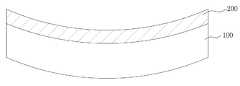
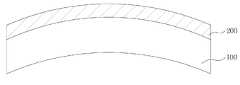
사파이어 기판 위에 질화갈륨을 성장시키는 경우 사파이어 기판과 질화갈륨의 열팽창계수 차이로 인하여 질화갈륨층 성장시 도 1a에 도시된 바와 같이 사파이어 기판(100)으로부터 질화갈륨층(200)으로 휨이 발생한다. 또한, 질화갈륨층 성장 후 냉각 과정에서는 도 1b에 도시한 바와 같이 반대 방향으로 휨이 발생하여 질화갈륨층엔 전체적으로 스트레스가 가해지므로, 사파이어 기판으로부터 분리된 후에도 질화갈륨 자립층(freestanding layer)의 내구성이 취약하게 된다.When gallium nitride is grown on a sapphire substrate, warpage occurs from the
이러한 휨을 방지하기 위하여 질화갈륨에 비하여 열팽창계수 차이가 큰 사파이어에 비해서 열팽창계수 차이가 비교적 작은 GaAs 기판을 사용하는 방안에 제안된 바 있지만, GaAs는 고가이고 열에 열화되는 단점이 있다.In order to prevent such warpage, a method of using a GaAs substrate having a relatively smaller thermal expansion coefficient difference than that of sapphire having a large thermal expansion coefficient difference compared to gallium nitride has been proposed, but GaAs has a disadvantage in that it is expensive and degrades in heat.
사파이어 기판 위에 질화갈륨을 성장시키는 경우 문제가 다른 하나는 사파이어 기판에서 성장한 질화갈륨 박막 또는 후막을 기판으로부터 분리하는 것이 용이하지 않다는 점이다. 사파이어 기판으로부터 성장한 질화갈륨을 분리하는 방법으로 는 레이저를 이용한 기계적 분리 방법이 있다.Another problem with growing gallium nitride on a sapphire substrate is that it is not easy to separate the gallium nitride thin film or thick film grown on the sapphire substrate from the substrate. As a method of separating gallium nitride grown from a sapphire substrate, there is a mechanical separation method using a laser.
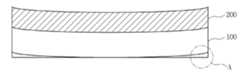
예를 들어, 도 2에 도시한 바와 같이 사이이어 기판(100)과 질화갈륨층(200)에 레이저를 조사하면 두 물질 사이의 계면에서 레이저에 의한 계면 융해가 발생하고, 그 결과 도 3에 도시한 바와 같이 질화갈륨층(200')을 사파이어 기판으로부터 분리할 수 있다.For example, as shown in FIG. 2, when the laser is irradiated onto the
그러나, 레이저를 이용한 질화갈륨층의 기계적 방식의 분리는 레이저 에너지 분포가 균일하여야 하고, 특히 크랙 발생이 용이한 질화갈륨층 가장자리 영역에서 응력이 집중되지 않도록 공정을 정밀하게 제어하여야 한다.However, the mechanical separation of the gallium nitride layer using a laser requires a uniform laser energy distribution, and in particular, the process must be precisely controlled so that stress is not concentrated in the edge region of the gallium nitride layer which is easily cracked.
질화갈륨 성장 과정 및 분리 과정에서 발생되는 질화갈륨의 휨은 다양한 소자에 응용되는데 제약이 되기때문에 생산성 및 제품 품질을 향상시킬 수 있는 개선된 질화갈륨 웨이퍼 제조 방법이 요청되고 있다.Since the warping of gallium nitride generated during gallium nitride growth and separation processes is limited to various devices, there is a need for an improved gallium nitride wafer manufacturing method that can improve productivity and product quality.
따라서, 본 발명의 목적은 휨이 감소된 고품질 질화갈륨 웨이퍼를 제공하는데 있다.It is therefore an object of the present invention to provide a high quality gallium nitride wafer with reduced warpage.
또한, 본 발명의 다른 목적은 질화갈륨 분리 과정에서 발생될 수 있는 국부적인 응력 집중을 제거하여 질화갈륨 웨이퍼의 품질을 향상하는데 있다.In addition, another object of the present invention is to improve the quality of the gallium nitride wafer by eliminating the local stress concentration that may occur during the gallium nitride separation process.
또한, 본 발명의 또 다른 목적은 생산성이 향상되고 수율이 우수한 질화갈륨 웨이퍼 제조 방법을 제공하는데 있다.In addition, another object of the present invention is to provide a gallium nitride wafer manufacturing method with improved productivity and excellent yield.
상기 목적을 달성하기 위하여, 베이스 기판 위에 질화갈륨층을 성장시키고, 상기 질화갈륨층의 성장 중 상기 베이스 기판 하면에 증착된 다결정 질화갈륨을 제거하고, 상기 질화갈륨층을 베이스 기판으로부터 분리하는 것을 특징으로 하는 질화갈륨 웨이퍼 제조 방법을 제공한다.In order to achieve the above object, a gallium nitride layer is grown on the base substrate, polycrystalline gallium nitride deposited on the lower surface of the base substrate during the growth of the gallium nitride layer, and the gallium nitride layer is separated from the base substrate A gallium nitride wafer manufacturing method is provided.
상기 다결정 질화갈륨의 제거는 기계적 연마 또는 화학적 식각에 의하여 수행될 수 있으며, 두 방법을 병행하는 것도 무방하다. 상기 질화갈륨층을 분리하는 단계는 베이스 기판에 레이저를 조사하여 질화갈륨층과 베이스 기판의 계면을 국부적으로 융해시킴으로써 분리할 수 있다.Removal of the polycrystalline gallium nitride may be performed by mechanical polishing or chemical etching, it is also possible to combine the two methods. The separating of the gallium nitride layer may be performed by locally melting the interface between the gallium nitride layer and the base substrate by irradiating a laser onto the base substrate.
본 발명에 따르면, 질화갈륨 웨이퍼 제조 시 질화갈륨 분리 공정의 수율을 향상시킬 뿐만 아니라, 질화갈륨 웨이퍼에 국부적으로 응력이 집중되는 것을 방지할 수 있다. 따라서 휨이 없고 내구성이 우수한 고품질 질화갈륨 기판을 제조할 수 있다. 또한, 질화갈륨 웨이퍼의 생산성 및 제조 수율을 향상시킬 수 있다.According to the present invention, it is possible not only to improve the yield of the gallium nitride separation process when manufacturing a gallium nitride wafer, but also to prevent local concentration of stress on the gallium nitride wafer. Therefore, a high quality gallium nitride substrate having no warpage and excellent durability can be manufactured. In addition, the productivity and manufacturing yield of the gallium nitride wafer can be improved.
기상에피탁시법을 이용하여 사파이어 등의 베이스 기판 위에 질화갈륨 벌크층을 성장시키는 경우 중요하게 대두되는 기술적 과제 중의 하나는 베이스 기판 위에 성장된 질화갈륨층을 분리시키는 공정이다. 분리 공정에는 레이저를 이용한 기계적 분리 및 산을 이용한 화학적 분리방법이 있다.When growing a gallium nitride bulk layer on a base substrate such as sapphire using gas phase epitaxy, one of the important technical problems is a process of separating the grown gallium nitride layer on the base substrate. Separation processes include mechanical separation using a laser and chemical separation using an acid.
레이저를 이용하는 방법은 예를 들어, 질화갈륨층이 일면에 성장된 사파이어 기판의 다른 면에 레이저를 입사시키면 레이저 에너지에 의해서 기판과 질화갈륨층 계면이 융해되어 질화갈륨층이 분리된다. 두께 내지 폭이 마이크로미터 수준인 계면 영역이 레이저로 융해(ablation) 될때에 발생되는 물질은 기체 액체 고체를 모두 포함하는 소위 플럼(plume)이라는 물질이 생성이 된다. 플럼 내의 조성은 고체 액체 기체로 되어진 Ga기 및 N기 그리고 Ga-N 화합물기가 존재한다. 이러한 플럼이 생성될 때 플럼 주변에 국부적(약 수 ㎛ 정도)으로 약 50,000℃ 까지 상승하게 된다.In the method using a laser, for example, when a laser is incident on another surface of a sapphire substrate on which a gallium nitride layer is grown on one side, the interface between the substrate and the gallium nitride layer is melted by the laser energy to separate the gallium nitride layer. The material generated when the interfacial area, which is about the thickness to the micrometer level, is laser-blended to produce a so-called plum, which contains all gaseous liquid solids. The composition in the plume contains Ga and N groups and Ga—N compound groups which are solid liquid gases. When such a plum is produced, it rises locally to about 50,000 ° C. around the plum.
이러한 급격한 온도 상승으로 인해 질화갈륨층과 베이스 기판 사이의 계면 영역(약 수 ㎛ 정도의 두께)이 용해된다. 레이저를 입사시킬 때 예를 들어 3.493 eV의 레이저를 균일한 에너지 세기로 베이스 기판을 통과시켜 질화갈륨층/베이스 기판 계면에 에너지 손실 없이 도달하도록 하고, 이 과정에서 베이스 기판 면적 전체적으로 질화갈륨층에 응력이 집중되는 것을 방지하는 것이 중요하다.This rapid temperature rise dissolves the interface region (thickness of about several micrometers) between the gallium nitride layer and the base substrate. When the laser is incident, for example, a 3.493 eV laser is passed through the base substrate with uniform energy intensity to reach the gallium nitride layer / base substrate interface without loss of energy, and in this process the stress on the gallium nitride layer as a whole of the base substrate area. It is important to prevent it from being concentrated.
그런데, 본 발명자들은 반복적인 실험 결과, 성장 공정 중에 (질화갈륨층과의 열팽창계수 차이에 기인하는) 베이스 기판의 휨으로 인하여 베이스 기판 하면에 다결정질의 질화갈륨(A)이 증착되며, 특히 이 휨은 가장자리로 갈수록 크게 되므로 가장자리 쪽에 불필요한 다결정질 질화갈륨이 많이 증착되는 것을 확인하였다(도 4 참조).However, the inventors have repeatedly observed that, during the growth process, polycrystalline gallium nitride (A) is deposited on the lower surface of the base substrate due to the warpage of the base substrate (due to the difference in the coefficient of thermal expansion with the gallium nitride layer). As it becomes larger toward the edge, it was confirmed that a lot of unnecessary polycrystalline gallium nitride is deposited on the edge side (see FIG. 4).
베이스 기판 하면에 불균일하게 형성된 다결정질 질화갈륨은 광학적 특성이 단결정 질화갈륨 보다 많이 떨어지므로 입사되는 레이저 에너지를 흡수하며, 결국 베이스 기판과 질화갈륨층 사이의 계면에 도달하는 레이저의 파워를 약화시킨다. 이로 인하여 베이스 기판과 질화갈륨층 계면에 도달하는 레이저의 에너지 분포가 도 5에서 볼 수 있듯이 중심(c)과 가장자리(e)가 다르게 되며, 결과적으로 계면에서 레이저에 의하여 융해되는 정도가 불균일하게 되어 질화갈륨층 분리시 치명적인 악영향을 끼친다.Polycrystalline gallium nitride non-uniformly formed on the lower surface of the base substrate absorbs the laser energy incident because optical properties are lower than that of the single crystal gallium nitride, thereby weakening the power of the laser reaching the interface between the base substrate and the gallium nitride layer. As a result, the energy distribution of the laser reaching the interface between the base substrate and the gallium nitride layer is different from the center (c) and the edge (e) as shown in FIG. 5, resulting in uneven melting of the laser at the interface. Separation of gallium nitride has a fatal adverse effect.
또한 베이스 기판의 가장자리 부분에 다결정 질화갈륨이 집중되어 질화갈륨층의 분리 공정시 응력 발생의 근원지가 되며, 따라서 질화갈륨층은 가장자리 부분에서 크랙이 발생이 용이해진다.In addition, the polycrystalline gallium nitride is concentrated at the edge of the base substrate, which becomes a source of stress during the separation process of the gallium nitride layer. Therefore, cracks are easily generated at the edge of the gallium nitride layer.
따라서, 본 발명자들은 베이스 하면에 원치않게 증착되는 불필요한 다결정 질화갈륨을 제거함으로써 질화갈륨 웨이퍼 제조 시 질화갈륨 분리 공정의 수율을 향상시킬 뿐만 아니라, 질화갈륨 웨이퍼에 국부적으로 응력이 집중되는 것을 방지할 수 있다.Accordingly, the present inventors can improve the yield of the gallium nitride separation process when manufacturing gallium nitride wafers by removing unnecessary polycrystalline gallium nitride that is undesirably deposited on the bottom surface of the base, and also prevent local stress concentration on the gallium nitride wafer. have.
본 발명은 도 6에 도시한 바와 같이 질화갈륨층을 베이스 기판 위에 성장시킨 후(단계 S1), 분리 공정을 진행하기 전에, 베이스 기판 하면에 형성된 다결정 질화갈륨을 제거한 후(단계 S2), 질화갈륨층을 베이스 기판으로부터 분리한다(단계 S3). 이와 같은 방법으로 질화갈륨층을 레이저를 사용하여 베이스 기판으로부터 분리할 때 분리되는 계면에 도달하는 레이저 에너지 분포를 균일하게 할 수 있고, 질화갈륨층에 국부적으로 응력이 야기되는 것을 방지할 수 있다.In the present invention, after the gallium nitride layer is grown on the base substrate as shown in FIG. 6 (step S1), the polycrystalline gallium nitride formed on the lower surface of the base substrate is removed (step S2) before the separation process is performed. The layer is separated from the base substrate (step S3). In this way, the laser energy distribution reaching the interface to be separated when the gallium nitride layer is separated from the base substrate by using a laser can be made uniform, and local stress can be prevented from occurring in the gallium nitride layer.
베이스 기판 하면에 원치않게 형성된 다결정질의 질화갈륨은 예를 들어 화학적인 방법으로 제거할 수 있다. 도 7을 참조하면, 식각액이 담겨있는 배쓰(bath)에 질화갈륨이 성장되어 있는 베이스 기판(120)을 담가 다결정 질화갈륨을 산으로 제거할 수 있다. 이와 같은 화학적 방법에 더불어 기계적인 방법(예를 들어, 연마, 래핑, 폴리싱 등)을 병행하여 베이스 기판 일면에 형성된 다결정 질화갈륨을 제거하는 것도 무방하다.Undesirably formed polycrystalline gallium nitride on the bottom surface of the base substrate can be removed, for example, by chemical methods. Referring to FIG. 7, the polycrystalline gallium nitride may be removed by immersing the
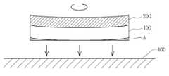
또한, 본 발명은 베이스 기판의 표면의 가장자리에 증착되어있는 다결정 질화갈륨층을 제거하기 위해 기계적인 연마를 이용할 수 있다. 다결정 질화갈륨은 질화갈륨 성장시 베이스 기판의 휨에 의하여 베이스 기판의 하면에 형성되는데, 특히 베이스 기판의 중심과 가장자리로부터 1/2이 되는 지점부터 가장자리까지의 영역에 집중되어 있다. 도 8의 모식도에 도시된 바와 같이 질화갈륨이 성장되어 있는 베이스 기판을 회전시키면서 연마 부재(400)에 베이스 기판 하면의 다결정 질화갈륨(A 부분)을 연마시킴으로써 다결정 질화갈륨을 효과적으로 제거할 수 있다. 베이스 기판 표면에 국부적으로 형성된 다결정 질화갈륨을 제거한 후에는 베이스 기판 면적에 대하여 전체적으로 레이저 투과율이 높아지고, 베이스 기판과 질화갈륨층 계면에 도달하는 레이저가 균일한 에너지 분포를 가질 수 있다.In addition, the present invention may utilize mechanical polishing to remove the polycrystalline gallium nitride layer deposited on the edge of the surface of the base substrate. Polycrystalline gallium nitride is formed on the lower surface of the base substrate by the bending of the base substrate during the growth of the gallium nitride, particularly concentrated in the area from the point half to the edge from the center and the edge of the base substrate. As shown in the schematic diagram of FIG. 8, polycrystalline gallium nitride can be effectively removed by polishing the polycrystalline gallium nitride (part A) of the lower surface of the base substrate on the
고정된 연마 부재에 상기 베이스 기판을 회전시키면서 베이스 기판 표면을 국부적으로 연마할 수도 있지만, 베이스 기판을 고정한 채로 연마 부재를 회전할 수도 있을 것이다. 또한, 기계적 연마(혹은 래핑)와 더불어 화학적 식각액 등을 함께 이용할 수 있다.While the base substrate surface may be locally polished while the base substrate is rotated to a fixed polishing member, the polishing member may be rotated while the base substrate is fixed. In addition, in addition to mechanical polishing (or lapping), a chemical etchant may be used together.
뿐만 아니라, 본 발명은 위에 제시한 화학적 방법과 기계적 방법을 조합하여 2 이상의 단계로 진행할 수도 있다.In addition, the present invention may proceed in two or more steps by combining the above-described chemical and mechanical methods.
본 발명은 일반적으로 질화갈륨 성장에 주로 사용되는 사파이어 기판, 단결 정 질화갈륨 기판 뿐만 아니라, ScAlMgO4(111)(Rhobohedral layered structure), SrTiO3, LaAlO3, LiNbO3, SrRuO3, ZnO, MgAl2O4(Spinel), LiAlO2(Distorted tetragonal), LiGaO2(Orthourhomic), AlN 등에 성장된 질화갈륨을 레이저를 이용하여 분리하는 시스템에도 효과적으로 적용될 수 있다.The present invention generally, as well as the sapphire substrate, unity positive gallium nitride substrate that is mainly used in the gallium nitridegrowth, ScAlMgO 4 (111) (Rhobohedral layered structure), SrTiO 3, LaAlO 3, LiNbO 3, SrRuO 3, ZnO,
이와 같은 개선된 공정으로 인하여 레이저를 이용하여 질화갈륨층을 베이스 기판으로부터 분리할 때 수율의 향상을 도모할 수 있었다.This improved process was able to improve the yield when the gallium nitride layer is separated from the base substrate using a laser.
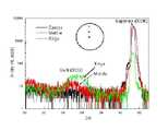
본 발명에 따른 질화갈륨 웨이퍼 제조 공정의 개선된 효과를 확인하기 위하여 베이스 기판의 다결정 질화갈륨 제거 전 후의 X-ray 회절 분석 결과를 조사하였다.In order to confirm the improved effect of the gallium nitride wafer manufacturing process according to the present invention, the results of X-ray diffraction analysis before and after polycrystalline gallium nitride removal of the base substrate were investigated.
도 9를 참조하면, 연마 전의 사파이어 기판 표면을 X-ray로 조사한 결과 사파이어 표면에 다결정 질화갈륨(0002) 피크가 매우 광범위하게 나타났으며, 이로 인하여 결정성이 좋지않은 다결정 질화갈륨이 사파이어 표면에 불필요하게 형성되었음을 알 수 있다. 또한 사파이어 기판의 가장자리로 갈수록 다결정 질화갈륨의 증착 정도가 많아짐을 알 수 있다.Referring to FIG. 9, X-ray irradiation of the surface of the sapphire substrate before polishing showed a very wide range of polycrystalline gallium nitride (0002) peaks on the sapphire surface, whereby polycrystalline gallium nitride having poor crystallinity was applied to the sapphire surface. It can be seen that it is formed unnecessarily. In addition, it can be seen that the deposition degree of polycrystalline gallium nitride increases as the edge of the sapphire substrate increases.
반면, 도 10을 참조하면, 사파이어 표면을 산으로 에칭한 후 X-ray 회절 분석 결과, 다결정 질화갈륨(0002) 피크가 소멸되었으며, 이로부터 사파이어 기판 표면에 국부적으로 형성된 다결정 질화갈륨이 제거되었음을 알 수 있다.On the other hand, referring to Figure 10, after etching the surface of the sapphire with acid X-ray diffraction analysis, the polycrystalline gallium nitride (0002) peak disappeared, it was found that the polycrystalline gallium nitride locally formed on the surface of the sapphire substrate was removed Can be.
산 에칭 및/또는 기계적 연마 후 베이스 기판 후면에 증착된 다결정 질화갈륨이 제거된 상태에서, 질화갈륨층을 베이스 기판으로부터 분리하였을 때 질화갈륨 의 휨이나 응력의 불균일한 집중에 따른 크랙 발생이 현저히 줄어들은 것을 확인하였다.With the removal of the polycrystalline gallium nitride deposited on the backside of the base substrate after acid etching and / or mechanical polishing, crack generation due to the uneven concentration of gallium nitride warpage or stress when the gallium nitride layer is separated from the base substrate is significantly reduced. Confirmed that.
이상에서 바람직한 실시예를 통하여 본 발명을 예시적으로 설명하였으나, 본 발명은 이와 같은 특정 실시예에만 한정되는 것은 아니며 본 발명에서 제시한 기술적 사상, 구체적으로는 특허청구범위에 기재된 범주 내에서 다양한 형태로 수정, 변경, 또는 개선될 수 있을 것이다.The present invention has been exemplarily described through the preferred embodiments, but the present invention is not limited to such specific embodiments, and various forms within the scope of the technical idea presented in the present invention, specifically, the claims. May be modified, changed, or improved.
도 1a 및 1b는 성장시 발생하는 질화갈륨층의 휨을 보인 모식도.Figure 1a and 1b is a schematic diagram showing the warpage of the gallium nitride layer generated during growth.
도 2는 레이저를 이용한 질화갈륨 분리 방법을 도시한 모식도.2 is a schematic diagram showing a gallium nitride separation method using a laser.
도 3은 기계적 방식으로 분리된 질화갈륨층을 보인 모식도.Figure 3 is a schematic diagram showing a gallium nitride layer separated in a mechanical manner.
도 4는 베이스 기판 하면에 국부적으로 형성된 다결정 질화갈륨을 보인 단면 모식도.4 is a schematic cross-sectional view showing polycrystalline gallium nitride locally formed on the bottom surface of a base substrate.
도 5는 베이스 기판과 질화갈륨층 계면에 도달하는 레이저 에너지 분포의 불균일을 보인 모식도.Fig. 5 is a schematic diagram showing the nonuniformity of laser energy distribution reaching the interface between the base substrate and the gallium nitride layer.
도 6은 본 발명에 따른 질화갈륨 웨이퍼 제조 공정을 보인 순서도.6 is a flow chart showing a gallium nitride wafer manufacturing process according to the present invention.
도 7은 화학적 방법으로 다결정 질화갈륨을 제거하는 방법을 보인 모식도.7 is a schematic diagram showing a method of removing polycrystalline gallium nitride by a chemical method.
도 8은 기계적 방법으로 다결정 질화갈륨을 제거하는 방법을 보인 모식도.8 is a schematic view showing a method of removing polycrystalline gallium nitride by a mechanical method.
도 9는 다결정 질화갈륨이 베이스 기판에 존재하는 것을 보인 X-ray 회절분석 결과.9 is an X-ray diffraction analysis showing that polycrystalline gallium nitride is present in the base substrate.
도 10은 본 발명에 따른 방법을 통하여 베이스 기판의 다결정 질화갈륨이 제거된 것을 보인 X-ray 회절분석 결과.10 is an X-ray diffraction analysis showing that the polycrystalline gallium nitride of the base substrate is removed through the method according to the present invention.
*** 도면의 주요 부분에 대한 부호의 설명 ****** Explanation of symbols for the main parts of the drawing ***
100:베이스 기판200:질화갈륨층100: base substrate 200: gallium nitride layer
300:배쓰400:연마 부재300: bath 400: polishing member
Claims (7)
Translated fromKoreanPriority Applications (1)
| Application Number | Priority Date | Filing Date | Title |
|---|---|---|---|
| KR1020070140219AKR101137905B1 (en) | 2007-12-28 | 2007-12-28 | Fabrication method of gallium nitride wafer |
Applications Claiming Priority (1)
| Application Number | Priority Date | Filing Date | Title |
|---|---|---|---|
| KR1020070140219AKR101137905B1 (en) | 2007-12-28 | 2007-12-28 | Fabrication method of gallium nitride wafer |
Publications (2)
| Publication Number | Publication Date |
|---|---|
| KR20090072183A KR20090072183A (en) | 2009-07-02 |
| KR101137905B1true KR101137905B1 (en) | 2012-05-03 |
Family
ID=41329436
Family Applications (1)
| Application Number | Title | Priority Date | Filing Date |
|---|---|---|---|
| KR1020070140219AExpired - Fee RelatedKR101137905B1 (en) | 2007-12-28 | 2007-12-28 | Fabrication method of gallium nitride wafer |
Country Status (1)
| Country | Link |
|---|---|
| KR (1) | KR101137905B1 (en) |
Cited By (1)
| Publication number | Priority date | Publication date | Assignee | Title |
|---|---|---|---|---|
| US9947530B2 (en) | 2016-06-14 | 2018-04-17 | Samsung Electronics Co., Ltd. | Method of manufacturing nitride semiconductor substrate |
Families Citing this family (1)
| Publication number | Priority date | Publication date | Assignee | Title |
|---|---|---|---|---|
| CN116065238A (en)* | 2021-06-17 | 2023-05-05 | 山东浪潮华光光电子股份有限公司 | GaN thick film growth method for reducing surface particles |
Citations (2)
| Publication number | Priority date | Publication date | Assignee | Title |
|---|---|---|---|---|
| KR20030052061A (en)* | 2001-12-20 | 2003-06-26 | 엘지전자 주식회사 | Apparatus and method of manufacturing GaN substrate |
| KR100678407B1 (en)* | 2003-03-18 | 2007-02-02 | 크리스탈 포토닉스, 인코포레이티드 | Method of manufacturing group III nitride device and device manufactured by this method |
- 2007
- 2007-12-28KRKR1020070140219Apatent/KR101137905B1/ennot_activeExpired - Fee Related
Patent Citations (2)
| Publication number | Priority date | Publication date | Assignee | Title |
|---|---|---|---|---|
| KR20030052061A (en)* | 2001-12-20 | 2003-06-26 | 엘지전자 주식회사 | Apparatus and method of manufacturing GaN substrate |
| KR100678407B1 (en)* | 2003-03-18 | 2007-02-02 | 크리스탈 포토닉스, 인코포레이티드 | Method of manufacturing group III nitride device and device manufactured by this method |
Cited By (1)
| Publication number | Priority date | Publication date | Assignee | Title |
|---|---|---|---|---|
| US9947530B2 (en) | 2016-06-14 | 2018-04-17 | Samsung Electronics Co., Ltd. | Method of manufacturing nitride semiconductor substrate |
Also Published As
| Publication number | Publication date |
|---|---|
| KR20090072183A (en) | 2009-07-02 |
Similar Documents
| Publication | Publication Date | Title |
|---|---|---|
| US8637848B2 (en) | Single crystal group III nitride articles and method of producing same by HVPE method incorporating a polycrystalline layer for yield enhancement | |
| KR100969812B1 (en) | Method for manufacturing gallium nitride single crystal substrate using self separation | |
| US9096950B2 (en) | Nitride crystal and method for producing the same | |
| KR20010029199A (en) | Device and method for forming nitride single crystalline substrate | |
| JP6526811B2 (en) | Method of processing a group III nitride crystal | |
| JP6405767B2 (en) | Gallium nitride substrate | |
| KR100907617B1 (en) | Method for producing gallium nitride substrate | |
| KR101137905B1 (en) | Fabrication method of gallium nitride wafer | |
| JPH1179897A (en) | Crystal growth for gallium nitride thick film | |
| KR100558436B1 (en) | Method of manufacturing gallium nitride single crystal substrate | |
| KR20050033911A (en) | Method of producing a gallium nitride based singlecrystal substrate | |
| KR101157426B1 (en) | Base substrate for gallium nitride, fabrication method of base substrate, and fabrication method of gallium nitride | |
| US20240387769A1 (en) | Method for producing a growth substrate, growth substrate, and method for producing a plurality of optoelectronic semiconductor chips | |
| KR100519326B1 (en) | method for fabricating substate of GaN semiconductor laser diode | |
| US20160076168A1 (en) | Substrates for growing group iii nitride crystals and their fabrication method | |
| JP2017214232A (en) | Method of manufacturing nitride compound semiconductor substrate | |
| JP2000269143A (en) | Method for producing gallium nitride-based compound semiconductor crystal | |
| WO2016040533A1 (en) | Substrates for growing group iii nitride crystals and their fabrication method | |
| KR101137910B1 (en) | A substrate for growing gallium nitride and a method for manufacturing a gallium nitride substrate | |
| KR101144844B1 (en) | Gallium nitride base substrate and fabrication method of gallium nitride wafer | |
| KR100438819B1 (en) | Method for fabricating GaN single crystal substrate | |
| KR20120038293A (en) | Method for manufacturing semiconductor substrate | |
| JPH0536602A (en) | Hexagonal semiconductor crystal growth method | |
| KR100890085B1 (en) | Nitride substrate manufacturing method | |
| US20140116327A1 (en) | Method and apparatus for fabricating free-standing group iii nitride crystals |
Legal Events
| Date | Code | Title | Description |
|---|---|---|---|
| PA0109 | Patent application | St.27 status event code:A-0-1-A10-A12-nap-PA0109 | |
| N231 | Notification of change of applicant | ||
| PN2301 | Change of applicant | St.27 status event code:A-3-3-R10-R13-asn-PN2301 St.27 status event code:A-3-3-R10-R11-asn-PN2301 | |
| PG1501 | Laying open of application | St.27 status event code:A-1-1-Q10-Q12-nap-PG1501 | |
| PN2301 | Change of applicant | St.27 status event code:A-3-3-R10-R13-asn-PN2301 St.27 status event code:A-3-3-R10-R11-asn-PN2301 | |
| A201 | Request for examination | ||
| PA0201 | Request for examination | St.27 status event code:A-1-2-D10-D11-exm-PA0201 | |
| E902 | Notification of reason for refusal | ||
| PE0902 | Notice of grounds for rejection | St.27 status event code:A-1-2-D10-D21-exm-PE0902 | |
| P11-X000 | Amendment of application requested | St.27 status event code:A-2-2-P10-P11-nap-X000 | |
| P13-X000 | Application amended | St.27 status event code:A-2-2-P10-P13-nap-X000 | |
| E701 | Decision to grant or registration of patent right | ||
| PE0701 | Decision of registration | St.27 status event code:A-1-2-D10-D22-exm-PE0701 | |
| GRNT | Written decision to grant | ||
| PR0701 | Registration of establishment | St.27 status event code:A-2-4-F10-F11-exm-PR0701 | |
| PR1002 | Payment of registration fee | St.27 status event code:A-2-2-U10-U11-oth-PR1002 Fee payment year number:1 | |
| PG1601 | Publication of registration | St.27 status event code:A-4-4-Q10-Q13-nap-PG1601 | |
| PN2301 | Change of applicant | St.27 status event code:A-5-5-R10-R13-asn-PN2301 St.27 status event code:A-5-5-R10-R11-asn-PN2301 | |
| R18-X000 | Changes to party contact information recorded | St.27 status event code:A-5-5-R10-R18-oth-X000 | |
| LAPS | Lapse due to unpaid annual fee | ||
| PC1903 | Unpaid annual fee | St.27 status event code:A-4-4-U10-U13-oth-PC1903 Not in force date:20150413 Payment event data comment text:Termination Category : DEFAULT_OF_REGISTRATION_FEE | |
| PN2301 | Change of applicant | St.27 status event code:A-5-5-R10-R13-asn-PN2301 St.27 status event code:A-5-5-R10-R11-asn-PN2301 | |
| PC1903 | Unpaid annual fee | St.27 status event code:N-4-6-H10-H13-oth-PC1903 Ip right cessation event data comment text:Termination Category : DEFAULT_OF_REGISTRATION_FEE Not in force date:20150413 | |
| P22-X000 | Classification modified | St.27 status event code:A-4-4-P10-P22-nap-X000 |