KR101137514B1 - Method for manufacturing nitride semiconductor device using nano particle - Google Patents
Method for manufacturing nitride semiconductor device using nano particleDownload PDFInfo
- Publication number
- KR101137514B1 KR101137514B1KR1020110021900AKR20110021900AKR101137514B1KR 101137514 B1KR101137514 B1KR 101137514B1KR 1020110021900 AKR1020110021900 AKR 1020110021900AKR 20110021900 AKR20110021900 AKR 20110021900AKR 101137514 B1KR101137514 B1KR 101137514B1
- Authority
- KR
- South Korea
- Prior art keywords
- nitride
- based semiconductor
- layer
- semiconductor device
- nanoparticle
- Prior art date
- Legal status (The legal status is an assumption and is not a legal conclusion. Google has not performed a legal analysis and makes no representation as to the accuracy of the status listed.)
- Active
Links
- 150000004767nitridesChemical class0.000titleclaimsabstractdescription127
- 239000004065semiconductorSubstances0.000titleclaimsabstractdescription127
- 239000002105nanoparticleSubstances0.000titleclaimsabstractdescription80
- 238000004519manufacturing processMethods0.000titleclaimsabstractdescription41
- 238000000034methodMethods0.000titleclaimsabstractdescription28
- 239000000758substrateSubstances0.000claimsabstractdescription74
- 238000004528spin coatingMethods0.000claimsabstractdescription14
- 229910018072Al 2 O 3Inorganic materials0.000claimsabstractdescription9
- 238000001039wet etchingMethods0.000claimsabstractdescription9
- 239000011259mixed solutionSubstances0.000claimsabstractdescription8
- XLOMVQKBTHCTTD-UHFFFAOYSA-NZinc monoxideChemical compound[Zn]=OXLOMVQKBTHCTTD-UHFFFAOYSA-N0.000claimsdescription11
- HBMJWWWQQXIZIP-UHFFFAOYSA-Nsilicon carbideChemical compound[Si+]#[C-]HBMJWWWQQXIZIP-UHFFFAOYSA-N0.000claimsdescription8
- JMASRVWKEDWRBT-UHFFFAOYSA-NGallium nitrideChemical compound[Ga]#NJMASRVWKEDWRBT-UHFFFAOYSA-N0.000claimsdescription6
- XUIMIQQOPSSXEZ-UHFFFAOYSA-NSiliconChemical compound[Si]XUIMIQQOPSSXEZ-UHFFFAOYSA-N0.000claimsdescription6
- 239000000395magnesium oxideSubstances0.000claimsdescription6
- CPLXHLVBOLITMK-UHFFFAOYSA-Nmagnesium oxideInorganic materials[Mg]=OCPLXHLVBOLITMK-UHFFFAOYSA-N0.000claimsdescription6
- AXZKOIWUVFPNLO-UHFFFAOYSA-Nmagnesium;oxygen(2-)Chemical compound[O-2].[Mg+2]AXZKOIWUVFPNLO-UHFFFAOYSA-N0.000claimsdescription6
- 238000000926separation methodMethods0.000claimsdescription6
- 229910052710siliconInorganic materials0.000claimsdescription6
- 239000010703siliconSubstances0.000claimsdescription6
- 238000001312dry etchingMethods0.000claimsdescription5
- 239000011787zinc oxideSubstances0.000claimsdescription5
- PIGFYZPCRLYGLF-UHFFFAOYSA-NAluminum nitrideChemical compound[Al]#NPIGFYZPCRLYGLF-UHFFFAOYSA-N0.000claimsdescription4
- JBRZTFJDHDCESZ-UHFFFAOYSA-NAsGaChemical compound[As]#[Ga]JBRZTFJDHDCESZ-UHFFFAOYSA-N0.000claimsdescription3
- 229910052581Si3N4Inorganic materials0.000claimsdescription3
- 229910004298SiO 2Inorganic materials0.000claimsdescription3
- VYPSYNLAJGMNEJ-UHFFFAOYSA-NSilicium dioxideChemical compoundO=[Si]=OVYPSYNLAJGMNEJ-UHFFFAOYSA-N0.000claimsdescription3
- TWNQGVIAIRXVLR-UHFFFAOYSA-Noxo(oxoalumanyloxy)alumaneChemical compoundO=[Al]O[Al]=OTWNQGVIAIRXVLR-UHFFFAOYSA-N0.000claimsdescription3
- HQVNEWCFYHHQES-UHFFFAOYSA-Nsilicon nitrideChemical compoundN12[Si]34N5[Si]62N3[Si]51N64HQVNEWCFYHHQES-UHFFFAOYSA-N0.000claimsdescription3
- 229910052814silicon oxideInorganic materials0.000claimsdescription3
- 239000000203mixtureSubstances0.000claimsdescription2
- 239000007921spraySubstances0.000claimsdescription2
- 239000010410layerSubstances0.000description116
- 229910052594sapphireInorganic materials0.000description13
- 239000010980sapphireSubstances0.000description13
- 239000000463materialSubstances0.000description9
- 239000006104solid solutionSubstances0.000description6
- 229910045601alloyInorganic materials0.000description5
- 239000000956alloySubstances0.000description5
- 238000005229chemical vapour depositionMethods0.000description5
- 239000010949copperSubstances0.000description5
- 229910052751metalInorganic materials0.000description5
- 239000002184metalSubstances0.000description5
- 229910010271silicon carbideInorganic materials0.000description5
- 238000000576coating methodMethods0.000description4
- RYGMFSIKBFXOCR-UHFFFAOYSA-NCopperChemical compound[Cu]RYGMFSIKBFXOCR-UHFFFAOYSA-N0.000description3
- 229910002601GaNInorganic materials0.000description3
- OKKJLVBELUTLKV-UHFFFAOYSA-NMethanolChemical compoundOCOKKJLVBELUTLKV-UHFFFAOYSA-N0.000description3
- 239000011651chromiumSubstances0.000description3
- 229910052802copperInorganic materials0.000description3
- 238000005520cutting processMethods0.000description3
- 125000005842heteroatomChemical group0.000description3
- IJGRMHOSHXDMSA-UHFFFAOYSA-NAtomic nitrogenChemical compoundN#NIJGRMHOSHXDMSA-UHFFFAOYSA-N0.000description2
- VYZAMTAEIAYCRO-UHFFFAOYSA-NChromiumChemical compound[Cr]VYZAMTAEIAYCRO-UHFFFAOYSA-N0.000description2
- ZOKXTWBITQBERF-UHFFFAOYSA-NMolybdenumChemical compound[Mo]ZOKXTWBITQBERF-UHFFFAOYSA-N0.000description2
- BQCADISMDOOEFD-UHFFFAOYSA-NSilverChemical compound[Ag]BQCADISMDOOEFD-UHFFFAOYSA-N0.000description2
- 229910052782aluminiumInorganic materials0.000description2
- XAGFODPZIPBFFR-UHFFFAOYSA-NaluminiumChemical compound[Al]XAGFODPZIPBFFR-UHFFFAOYSA-N0.000description2
- 229910052804chromiumInorganic materials0.000description2
- 239000011248coating agentSubstances0.000description2
- 238000002248hydride vapour-phase epitaxyMethods0.000description2
- 238000012986modificationMethods0.000description2
- 230000004048modificationEffects0.000description2
- 229910052750molybdenumInorganic materials0.000description2
- 239000011733molybdenumSubstances0.000description2
- 229910021421monocrystalline siliconInorganic materials0.000description2
- 238000005289physical depositionMethods0.000description2
- 238000005240physical vapour depositionMethods0.000description2
- 238000000746purificationMethods0.000description2
- 229910052709silverInorganic materials0.000description2
- 239000004332silverSubstances0.000description2
- 239000000243solutionSubstances0.000description2
- 239000002904solventSubstances0.000description2
- 238000000638solvent extractionMethods0.000description2
- 238000004544sputter depositionMethods0.000description2
- XLYOFNOQVPJJNP-UHFFFAOYSA-NwaterSubstancesOXLYOFNOQVPJJNP-UHFFFAOYSA-N0.000description2
- 229910000838Al alloyInorganic materials0.000description1
- GYHNNYVSQQEPJS-UHFFFAOYSA-NGalliumChemical compound[Ga]GYHNNYVSQQEPJS-UHFFFAOYSA-N0.000description1
- 239000002253acidSubstances0.000description1
- AUCDRFABNLOFRE-UHFFFAOYSA-Nalumane;indiumChemical compound[AlH3].[In]AUCDRFABNLOFRE-UHFFFAOYSA-N0.000description1
- RNQKDQAVIXDKAG-UHFFFAOYSA-Naluminum galliumChemical compound[Al].[Ga]RNQKDQAVIXDKAG-UHFFFAOYSA-N0.000description1
- 229910021417amorphous siliconInorganic materials0.000description1
- NWAIGJYBQQYSPW-UHFFFAOYSA-NazanylidyneindiganeChemical compound[In]#NNWAIGJYBQQYSPW-UHFFFAOYSA-N0.000description1
- 238000005234chemical depositionMethods0.000description1
- SBYXRAKIOMOBFF-UHFFFAOYSA-Ncopper tungstenChemical compound[Cu].[W]SBYXRAKIOMOBFF-UHFFFAOYSA-N0.000description1
- PMHQVHHXPFUNSP-UHFFFAOYSA-Mcopper(1+);methylsulfanylmethane;bromideChemical compoundBr[Cu].CSCPMHQVHHXPFUNSP-UHFFFAOYSA-M0.000description1
- 238000005336crackingMethods0.000description1
- 239000013078crystalSubstances0.000description1
- 230000007423decreaseEffects0.000description1
- 239000008367deionised waterSubstances0.000description1
- 229910021641deionized waterInorganic materials0.000description1
- 238000000151depositionMethods0.000description1
- 229910003460diamondInorganic materials0.000description1
- 239000010432diamondSubstances0.000description1
- 230000000694effectsEffects0.000description1
- 238000005530etchingMethods0.000description1
- 229910052733galliumInorganic materials0.000description1
- 229910052738indiumInorganic materials0.000description1
- APFVFJFRJDLVQX-UHFFFAOYSA-Nindium atomChemical compound[In]APFVFJFRJDLVQX-UHFFFAOYSA-N0.000description1
- 239000012212insulatorSubstances0.000description1
- 229910000765intermetallicInorganic materials0.000description1
- 230000001678irradiating effectEffects0.000description1
- 230000008018meltingEffects0.000description1
- 238000002844meltingMethods0.000description1
- 150000002739metalsChemical class0.000description1
- 238000001451molecular beam epitaxyMethods0.000description1
- 239000002103nanocoatingSubstances0.000description1
- 229910052757nitrogenInorganic materials0.000description1
- 229910021420polycrystalline siliconInorganic materials0.000description1
- 239000000843powderSubstances0.000description1
- 150000003839saltsChemical class0.000description1
- 238000007493shaping processMethods0.000description1
- 229910021332silicideInorganic materials0.000description1
- FVBUAEGBCNSCDD-UHFFFAOYSA-Nsilicide(4-)Chemical compound[Si-4]FVBUAEGBCNSCDD-UHFFFAOYSA-N0.000description1
- 238000001228spectrumMethods0.000description1
- 238000005507sprayingMethods0.000description1
- 230000001954sterilising effectEffects0.000description1
- 238000004659sterilization and disinfectionMethods0.000description1
- 239000000126substanceSubstances0.000description1
- 230000007704transitionEffects0.000description1
- WFKWXMTUELFFGS-UHFFFAOYSA-NtungstenChemical compound[W]WFKWXMTUELFFGS-UHFFFAOYSA-N0.000description1
- 229910052721tungstenInorganic materials0.000description1
- 239000010937tungstenSubstances0.000description1
- 238000000927vapour-phase epitaxyMethods0.000description1
Images


Classifications
- H—ELECTRICITY
- H01—ELECTRIC ELEMENTS
- H01L—SEMICONDUCTOR DEVICES NOT COVERED BY CLASS H10
- H01L21/00—Processes or apparatus adapted for the manufacture or treatment of semiconductor or solid state devices or of parts thereof
- H01L21/02—Manufacture or treatment of semiconductor devices or of parts thereof
- H01L21/02104—Forming layers
- H01L21/02365—Forming inorganic semiconducting materials on a substrate
- H01L21/02436—Intermediate layers between substrates and deposited layers
- H01L21/02494—Structure
- H01L21/02513—Microstructure
- H—ELECTRICITY
- H01—ELECTRIC ELEMENTS
- H01L—SEMICONDUCTOR DEVICES NOT COVERED BY CLASS H10
- H01L21/00—Processes or apparatus adapted for the manufacture or treatment of semiconductor or solid state devices or of parts thereof
- H01L21/02—Manufacture or treatment of semiconductor devices or of parts thereof
- H01L21/02104—Forming layers
- H01L21/02107—Forming insulating materials on a substrate
- H01L21/02109—Forming insulating materials on a substrate characterised by the type of layer, e.g. type of material, porous/non-porous, pre-cursors, mixtures or laminates
- H01L21/02112—Forming insulating materials on a substrate characterised by the type of layer, e.g. type of material, porous/non-porous, pre-cursors, mixtures or laminates characterised by the material of the layer
- H01L21/02172—Forming insulating materials on a substrate characterised by the type of layer, e.g. type of material, porous/non-porous, pre-cursors, mixtures or laminates characterised by the material of the layer the material containing at least one metal element, e.g. metal oxides, metal nitrides, metal oxynitrides or metal carbides
- H01L21/02175—Forming insulating materials on a substrate characterised by the type of layer, e.g. type of material, porous/non-porous, pre-cursors, mixtures or laminates characterised by the material of the layer the material containing at least one metal element, e.g. metal oxides, metal nitrides, metal oxynitrides or metal carbides characterised by the metal
- H01L21/02178—Forming insulating materials on a substrate characterised by the type of layer, e.g. type of material, porous/non-porous, pre-cursors, mixtures or laminates characterised by the material of the layer the material containing at least one metal element, e.g. metal oxides, metal nitrides, metal oxynitrides or metal carbides characterised by the metal the material containing aluminium, e.g. Al2O3
- H—ELECTRICITY
- H01—ELECTRIC ELEMENTS
- H01L—SEMICONDUCTOR DEVICES NOT COVERED BY CLASS H10
- H01L21/00—Processes or apparatus adapted for the manufacture or treatment of semiconductor or solid state devices or of parts thereof
- H01L21/02—Manufacture or treatment of semiconductor devices or of parts thereof
- H01L21/02104—Forming layers
- H01L21/02365—Forming inorganic semiconducting materials on a substrate
- H01L21/02436—Intermediate layers between substrates and deposited layers
- H01L21/02439—Materials
- H01L21/02455—Group 13/15 materials
- H01L21/02458—Nitrides
- H—ELECTRICITY
- H01—ELECTRIC ELEMENTS
- H01L—SEMICONDUCTOR DEVICES NOT COVERED BY CLASS H10
- H01L21/00—Processes or apparatus adapted for the manufacture or treatment of semiconductor or solid state devices or of parts thereof
- H01L21/02—Manufacture or treatment of semiconductor devices or of parts thereof
- H01L21/02104—Forming layers
- H01L21/02365—Forming inorganic semiconducting materials on a substrate
- H01L21/02612—Formation types
- H01L21/02617—Deposition types
- H01L21/02623—Liquid deposition
- H—ELECTRICITY
- H01—ELECTRIC ELEMENTS
- H01L—SEMICONDUCTOR DEVICES NOT COVERED BY CLASS H10
- H01L21/00—Processes or apparatus adapted for the manufacture or treatment of semiconductor or solid state devices or of parts thereof
- H01L21/02—Manufacture or treatment of semiconductor devices or of parts thereof
- H01L21/02104—Forming layers
- H01L21/02365—Forming inorganic semiconducting materials on a substrate
- H01L21/02656—Special treatments
- H01L21/02664—Aftertreatments
Landscapes
- Engineering & Computer Science (AREA)
- Physics & Mathematics (AREA)
- Condensed Matter Physics & Semiconductors (AREA)
- General Physics & Mathematics (AREA)
- Manufacturing & Machinery (AREA)
- Computer Hardware Design (AREA)
- Microelectronics & Electronic Packaging (AREA)
- Power Engineering (AREA)
- Chemical & Material Sciences (AREA)
- Crystallography & Structural Chemistry (AREA)
- Led Devices (AREA)
- Crystals, And After-Treatments Of Crystals (AREA)
Abstract
Translated fromKoreanDescription
Translated fromKorean본 발명은 질화물계 반도체 소자의 제조 방법에 관한 것으로, 더욱 상세하게는 이종 기판에 양질의 질화물계 반도체층을 형성한 후 질화물계 반도체층을 이종 기판에서 손상을 최소화하면서 분리하여 질화물계 반도체 소자를 제조하는 나노 입자를 이용한 질화물계 반도체 소자의 제조 방법에 관한 것이다.The present invention relates to a method of manufacturing a nitride-based semiconductor device, and more particularly to forming a nitride-based semiconductor device by forming a high-quality nitride-based semiconductor layer on a heterogeneous substrate and separating the nitride-based semiconductor layer while minimizing damage to the heterogeneous substrate. The present invention relates to a method for producing a nitride based semiconductor device using nanoparticles to be produced.
일반적으로 질소(N)와 같은 Ⅴ족 소스와, 갈륨(Ga), 알루미늄(Al) 또는 인듐(In)과 같은 Ⅲ족 소스를 포함하는 질화갈륨(GaN), 질화알루미늄(AlN), 질화인듐 (InN) 등의 질화물계 반도체 소재는 열적 안정성이 우수하고 직접 천이형의 에너지 밴드(band) 구조를 갖고 있어, 질화물계 반도체 소자 예컨대, 자외선 영역의 질화물계 반도체 발광소자, 태양전지소자 등으로 많이 사용되고 있다. 질화인듐알루미늄(AlInN)계 물질은 0.7eV에서 6.2eV의 폭넓은 에너지 밴드 갭을 가지고 있어 태양광스펙트럼 영역과 일치하는 특성으로 인하여 태양전지소자용 물질로 많이 사용되고 있다. 특히, 질화알루미늄갈륨(AlGaN)을 이용한 자외선 발광소자는 경화기 장치, 의료분석기 및 치료기기 및 살균, 정수, 정화시스템 등 다양한 산업분야에서 활용되고 있으며, 향후 반도체 조명 광원으로써 일반조명에 사용 가능한 물질로서 주목을 받고 있다.In general, gallium nitride (GaN), aluminum nitride (AlN), indium nitride (including Group V sources such as nitrogen (N) and group III sources such as gallium (Ga), aluminum (Al) or indium (In)) Nitride-based semiconductor materials such as InN) have excellent thermal stability and have a direct transition type energy band structure, and thus are widely used for nitride-based semiconductor devices such as nitride-based semiconductor light emitting devices and solar cell devices in the ultraviolet region. have. Indium aluminum nitride (AlInN) -based materials have a wide energy band gap of 0.7 eV to 6.2 eV, and thus are widely used as materials for solar cell devices due to their characteristics consistent with the solar spectrum region. In particular, ultraviolet light emitting devices using aluminum gallium nitride (AlGaN) are used in various industrial fields such as curing devices, medical analyzers and treatment devices, and sterilization, water purification, and purification systems. I'm getting attention.
이러한 질화물계 반도체 소재를 이용하여 성장시킨 질화물계 반도체층은 특히, 질화갈륨은 그것을 성장시킬 수 있는 동종의 기판을 제작하기가 어려워 유사한 결정 구조를 갖는 이종(hetero) 기판 위에 금속 유기 화학 기상 증착법(metal organic chemical vapor deposition; MOCVD) 또는 분자선 성장법(molecular beam epitaxy; MBE) 등의 공정을 통해 성장된다. 이종 기판으로는 육방 정계의 구조를 갖는 사파이어(Sapphire, Al2O3)나 실리콘 카바이드(SiC) 등이 사용되고 있다.In the nitride-based semiconductor layer grown using such a nitride-based semiconductor material, it is difficult to fabricate a homogeneous substrate capable of growing gallium nitride, in particular, a metal organic chemical vapor deposition method on a hetero substrate having a similar crystal structure. metal organic chemical vapor deposition (MOCVD) or molecular beam epitaxy (MBE). As the different substrates, sapphire (Sapphire, Al2 O3 ), silicon carbide (SiC), or the like having a hexagonal structure is used.
질화물계 반도체 소자 제조에 있어서, 이종 기판 중 사파이어 기판은 화학적 및 열적으로 안정적이며, 고온 제조공정을 가능케 하는 고융점을 갖고 있고, 높은 유전상수를 갖는다는 장점을 갖고 있다. 하지만 사파이어 기판은 열전도성이 떨어짐에 따라 궁극적으로 고휘도의 질화물계 반도체 소자를 제작하기 어려운 단점이 있다. 또한 사파이어는 전기적으로 부도체이므로 발광다이오드 구조를 제한하며, 기계적 및 화학적으로 매우 안정하여 절단 및 형상화(shaping) 등의 가공이 어려움 문제점을 갖고 있다. In the manufacture of nitride-based semiconductor devices, sapphire substrates among heterogeneous substrates are chemically and thermally stable, have a high melting point to enable a high temperature manufacturing process, and have a high dielectric constant. However, the sapphire substrate has a disadvantage in that it is difficult to manufacture a nitride-based semiconductor device of high brightness ultimately due to poor thermal conductivity. In addition, since sapphire is an electrically insulator, the structure of the light emitting diode is limited, and mechanically and chemically, the sapphire has a problem of difficulty in cutting and shaping.
이와 같은 문제점을 해소하기 위해서, 최근에는 사파이어와 같은 이종 기판 상에 질화물계 반도체층을 성장시킨 후, 이종 기판을 분리하여 발광 효율이 높은 질화물계 반도체 소자의 제조 방법에 따른 연구가 진행되고 있다.In order to solve such a problem, in recent years, a nitride semiconductor layer is grown on a dissimilar substrate such as sapphire, and then, a heterogeneous substrate is separated and a research on a method of manufacturing a nitride-based semiconductor device with high luminous efficiency has been conducted.
여기서 사파이어 기판과 질화물계 반도체 소자의 분리 공정에 있어 중요한 점은, 질화물계 반도체 소자의 특성을 안정적으로 담보하기 위해 사파이어 기판과 질화물계 반도체 소자의 분리 시 질화물계 반도체층의 크랙(crack) 발생을 최소화하여야 한다는 것이다.An important point in the separation process between the sapphire substrate and the nitride semiconductor device is that cracks of the nitride semiconductor layer are generated when the sapphire substrate and the nitride semiconductor device are separated in order to secure the characteristics of the nitride semiconductor device. It should be minimized.
사파이어 기판과 질화물계 반도체 소자를 분리시키는 방법으로, 주로 사파이어 기판과 질화물계 반도체 소자의 질화물계 반도체층의 계면에 레이저(laser)를 조사하여 분리시키는 이른바 레이저 리프트 오프(Laser Lift Off; LLO) 방법이 사용되고 있다.As a method of separating the sapphire substrate and the nitride semiconductor device, the so-called laser lift off (LLO) method is mainly performed by irradiating a laser at the interface between the sapphire substrate and the nitride semiconductor layer of the nitride semiconductor device. Is being used.
그러나 레이저 리프트 오프 방법은 레이저의 높은 열로 인해 질화물계 반도체 소자의 질화물계 반도체층을 열화시키거나, 열팽창계수의 차이로 인해 질화물계 반도체층 내에 크랙을 발생시키는 문제점이 있다.However, the laser lift-off method has a problem in that the nitride-based semiconductor layer of the nitride-based semiconductor device is degraded due to the high heat of the laser, or a crack is generated in the nitride-based semiconductor layer due to the difference in the thermal expansion coefficient.
한편 사파이어의 낮은 열전도도 특성을 극복하기 위해 사파이어 기판 대신 실리콘 카바이드 기판, 실리콘 기판을 적용하는 연구가 진행되고 있으나, 실리콘 카바이드 기판의 경우 기판 자체가 고가임에 따라 생산성이 떨어지는 문제가 있다. 실리콘 기판의 경우 가격이 저렴하고 우수한 열전도도 특성을 갖는 장점이 있으나, 질화물계 반도체층의 두께가 두꺼워질수록 열팽창계수 차이로 인한 크랙 문제가 심화되는 단점이 있다.On the other hand, in order to overcome the low thermal conductivity of sapphire, research is being conducted to apply silicon carbide substrates and silicon substrates instead of sapphire substrates. However, silicon carbide substrates have a problem in that productivity decreases as the substrate itself is expensive. In the case of a silicon substrate, it is inexpensive and has excellent thermal conductivity. However, as the thickness of the nitride-based semiconductor layer becomes thicker, there is a disadvantage in that a cracking problem due to a difference in thermal expansion coefficient is intensified.
따라서 본 발명의 목적은 이종 기판과 질화물계 반도체 소자의 분리 시 질화물계 반도체 소자의 손상을 최소화할 수 있는 나노 입자를 이용한 질화물계 반도체 소자의 제조 방법에 관한 것이다.Therefore, an object of the present invention relates to a method of manufacturing a nitride-based semiconductor device using nanoparticles that can minimize the damage of the nitride-based semiconductor device when separating the dissimilar substrate and the nitride-based semiconductor device.
본 발명의 다른 목적은 이종 기판 위에 양질의 질화물계 반도체층을 성장시킬 수 있는 나노 입자를 이용한 질화물계 반도체 소자의 제조 방법에 관한 것이다.Another object of the present invention relates to a method for manufacturing a nitride-based semiconductor device using nanoparticles capable of growing a high quality nitride-based semiconductor layer on a dissimilar substrate.
본 발명의 또 다른 목적은 질화물계 반도체층 분리 공정을 간소화하면서 저비용으로 질화물계 반도체 소자를 제조할 수 있는 나노 입자를 이용한 질화물계 반도체 소자의 제조 방법에 관한 것이다.Still another object of the present invention is to provide a method of manufacturing a nitride-based semiconductor device using nanoparticles which can manufacture a nitride-based semiconductor device at a low cost while simplifying a nitride-based semiconductor layer separation process.
상기 목적을 달성하기 위하여, 본 발명은 이종 기판 위에 유전체층을 형성하는 유전체층 형성 단계, 상기 유전체층 위에 Al2O3의 나노입자를 함유한 혼합액을 도포하여 다층의 나노입자층을 형성하는 나노입자층 형성 단계, 상기 나노입자층 위에 질화물계 반도체층을 형성하는 질화물계 반도체층 형성 단계, 상기 질화물계 반도체층 위에 지지기판을 접합하는 접합 단계, 상기 나노입자층 아래의 상기 유전체층이 형성된 상기 이종 기판을 분리하는 분리 단계, 및 상기 나노입자층을 제거하여 상기 지지기판 위에 상기 질화물계 반도체층이 형성된 질화물계 반도체 소자를 획득하는 획득 단계를 포함하는 나노 입자를 이용한 질화물계 반도체 소자의 제조 방법을 제공한다.In order to achieve the above object, the present invention provides a dielectric layer forming step of forming a dielectric layer on a heterogeneous substrate, nanoparticle layer forming step of forming a multi-layer nanoparticle layer by applying a mixed solution containing Al2 O3 nanoparticles on the dielectric layer, A nitride-based semiconductor layer forming step of forming a nitride-based semiconductor layer on the nanoparticle layer, a bonding step of bonding a support substrate on the nitride-based semiconductor layer, a separation step of separating the heterogeneous substrate on which the dielectric layer is formed below the nanoparticle layer; And an obtaining step of removing the nanoparticle layer to obtain a nitride based semiconductor device having the nitride based semiconductor layer formed on the support substrate.
본 발명에 따른 질화물계 반도체 소자의 제조 방법에 있어서, 상기 유전체층 형성 단계에서, 상기 이종 기판은 사파이어(Al2O3), 실리콘(Si), 징크 옥사이드(zinc oxide, ZnO), 갈륨 나이트라이드(gallium nitride, GaN), 갈륨 비소(GaAs), 실리콘 카바이드(silicon carbide, SiC), 알루미늄 나이트라이드(AlN) 또는 산화 마그네슘(MgO) 소재의 기판이 사용될 수 있다. 상기 유전체층은 상기 이종 기판 위에 100 내지 200nm의 두께로 형성된 실리콘산화막(SiO2) 또는 실리콘질화막(SiN) 중에 하나가 사용될 수 있다.In the method of manufacturing a nitride-based semiconductor device according to the present invention, in the dielectric layer forming step, the hetero substrate is sapphire (Al2 O3 ), silicon (Si), zinc oxide (ZincO, ZnO), gallium nitride ( Substrates made of gallium nitride (GaN), gallium arsenide (GaAs), silicon carbide (SiC), aluminum nitride (AlN) or magnesium oxide (MgO) may be used. The dielectric layer may be one of a silicon oxide film (SiO2 ) or a silicon nitride film (SiN) formed to have a thickness of 100 to 200 nm on the heterogeneous substrate.
본 발명에 따른 질화물계 반도체 소자의 제조 방법에 있어서, 상기 나노입자층 형성 단계에서, 상기 혼합액을 스핀 코팅으로 도포하여 1㎛ 이하의 두께를 갖는 다중층으로 상기 나노입자층을 형성할 수 있다.In the method for manufacturing a nitride-based semiconductor device according to the present invention, in the nanoparticle layer forming step, it is possible to form the nanoparticle layer in a multi-layer having a thickness of 1㎛ or less by applying the mixture by spin coating.
본 발명에 따른 질화물계 반도체 소자의 제조 방법에 있어서, 상기 나노입자층 형성 단계는 스핀 코팅, 스프레이 또는 딥인 방법으로 수행될 수 있다.In the method of manufacturing a nitride-based semiconductor device according to the invention, the nanoparticle layer forming step may be performed by a method of spin coating, spraying or dip.
본 발명에 따른 질화물계 반도체 소자의 제조 방법에 있어서, 상기 질화물계 반도체층 형성 단계는, 상기 나노입자층 위에 질화물계 반도체층을 성장시키는 단계와, 상기 질화물계 반도체층을 제조될 질화물계 반도체 소자에 대응되게 분할하는 분할 단계를 포함할 수 있다.In the method of manufacturing a nitride-based semiconductor device according to the present invention, the forming of the nitride-based semiconductor layer, the step of growing a nitride-based semiconductor layer on the nanoparticle layer, and the nitride-based semiconductor device to be manufactured It may include a partitioning step of correspondingly partitioning.
본 발명에 따른 질화물계 반도체 소자의 제조 방법에 있어서, 상기 분할 단계에서, 건식 식각으로 상기 나노입자층이 노출되게 상기 질화물계 반도체층을 분할할 수 있다.In the method of manufacturing a nitride based semiconductor device according to the present invention, in the dividing step, the nitride based semiconductor layer may be divided so that the nanoparticle layer is exposed by dry etching.
그리고 본 발명에 따른 질화물계 반도체 소자의 제조 방법에 있어서, 상기 분리 단계에서, 상기 유전체층이 형성된 상기 이종 기판을 습식 식각이나 초음파 세척기를 이용하여 상기 나노입자층에서 분리할 수 있다.In the method for manufacturing a nitride-based semiconductor device according to the present invention, in the separation step, the heterogeneous substrate on which the dielectric layer is formed may be separated from the nanoparticle layer using a wet etching or an ultrasonic cleaner.
본 발명에 따르면, 나노입자층을 스핀 코팅을 이용하여 이종 기판 위에 다층으로 형성한 후, 나노입자층 위에 질화물계 반도체층을 형성함으로써, 나노입자층에 의해 스트레인과 전위 밀도가 감소한 양질의 질화물계 반도체층을 갖는 질화물계 반도체 소자를 제조할 수 있다.According to the present invention, by forming a nanoparticle layer in multiple layers on a heterogeneous substrate using spin coating, and then forming a nitride-based semiconductor layer on the nanoparticle layer, a high quality nitride-based semiconductor layer is reduced strain and dislocation density by the nanoparticle layer The nitride semiconductor element which has it can be manufactured.
또한 스핀 코팅과 같은 도포 방법을 이용하여 다층으로 형성된 나노입자층을 경계로 질화물계 반도체층을 습식 식각이나 초음파 세척기를 이용하여 이종 기판에서 분리하여 질화물계 반도체 소자를 제조할 수 있기 때문에, 나노입자층을 스퍼터링과 같은 물리적인 증착으로 형성하고 레이저 리프트 오프 방식을 이용하여 질화물계 반도체층을 분리하는 것에 비해서 질화물계 반도체층의 손상을 최소화하면서, 제조 공정을 간소화할 수 있고, 또한 질화물계 반도체 소자의 제조 비용을 낮출 수 있는 이점이 있다.In addition, since the nitride-based semiconductor layer may be separated from the heterogeneous substrate by wet etching or an ultrasonic cleaner using a coating method such as spin coating, the nitride-based semiconductor layer may be manufactured using a wet etching method or an ultrasonic cleaner, thereby forming the nanoparticle layer. Compared with the physical vapor deposition such as sputtering and separating the nitride semiconductor layer by using a laser lift-off method, the manufacturing process can be simplified while minimizing damage to the nitride semiconductor layer. There is an advantage to lower the cost.
도 1은 본 발명의 실시예에 따른 나노 입자를 이용한 질화물계 반도체 소자의 제조 방법에 따른 흐름도이다.
도 2 내지 8은 도 1의 제조 방법에 따른 각 단계를 보여주는 도면으로서,
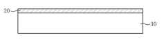
도 2는 이종 기판 위에 유전체층이 형성된 상태를 보여주는 단면도이고,
도 3은 유전체층 위에 스핀 코팅으로 다층의 나노입자층이 형성된 상태를 보여주는 단면도이고,
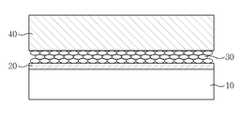
도 4는 다층의 나노입자층 위에 질화물계 반도체층이 성장된 상태를 보여주는 단면도이고,
도 5는 질화물계 반도체층을 분리할 질화물계 반도체 소자에 대응되게 분할된 상태를 보여주는 단면도이고,
도 6은 분할된 질화물계 반도체층 위에 지지기판이 접합된 상태를 보여주는 단면도이고,
도 7은 습식 식각을 통해서 이종 기판을 분리하는 과정을 보여주는 단면도이고,
도 8은 나노입자층을 제거하여 획득한 질화물계 반도체 소자를 보여주는 단면도이다.1 is a flowchart illustrating a method of manufacturing a nitride based semiconductor device using nanoparticles according to an embodiment of the present invention.
2 to 8 are views showing each step according to the manufacturing method of FIG.
2 is a cross-sectional view illustrating a state in which a dielectric layer is formed on a heterogeneous substrate.
3 is a cross-sectional view showing a state in which a multilayer nanoparticle layer is formed by spin coating on a dielectric layer,
4 is a cross-sectional view illustrating a nitride-based semiconductor layer grown on a multi-layer nanoparticle layer;
5 is a cross-sectional view illustrating a state in which a nitride based semiconductor layer is divided to correspond to a nitride based semiconductor device to be separated;
6 is a cross-sectional view illustrating a state in which a supporting substrate is bonded on a divided nitride based semiconductor layer.
7 is a cross-sectional view illustrating a process of separating heterogeneous substrates through wet etching;
8 is a cross-sectional view illustrating a nitride based semiconductor device obtained by removing a nanoparticle layer.
하기의 설명에서는 본 발명의 실시예에 따른 동작을 이해하는데 필요한 부분만이 설명되며, 그 이외 부분의 설명은 본 발명의 요지를 흩트리지 않도록 생략될 것이라는 것을 유의하여야 한다.In the following description, only parts necessary for understanding the operation according to the embodiment of the present invention will be described, it should be noted that the description of other parts will be omitted so as not to distract from the gist of the present invention.
또한 이하에서 설명되는 본 명세서 및 청구범위에 사용된 용어나 단어는 통상적이거나 사전적인 의미로 한정해서 해석되어서는 아니 되며, 발명자는 그 자신의 발명을 가장 최선의 방법으로 설명하기 위해 용어의 개념으로 적절하게 정의할 수 있다는 원칙에 입각하여 본 발명의 기술적 사상에 부합하는 의미와 개념으로 해석되어야만 한다. 따라서 본 명세서에 기재된 실시예와 도면에 도시된 구성은 본 발명의 바람직한 하나의 실시예에 불과할 뿐이고, 본 발명의 기술적 사상을 모두 대변하는 것은 아니므로, 본 출원시점에 있어서 이들을 대체할 수 있는 다양한 균등물과 변형예들이 있을 수 있음을 이해하여야 한다.Also, the terms and words used in the present specification and claims should not be construed to be limited to ordinary or dictionary meanings, and the inventor is not limited to the concept of terms in order to describe his invention in the best way. It should be construed in accordance with the meaning and concept consistent with the technical idea of the present invention based on the principle that it can be properly defined. Therefore, the embodiments described in the present specification and the configurations shown in the drawings are merely one preferred embodiment of the present invention, and not all of the technical ideas of the present invention are described. Therefore, It is to be understood that equivalents and modifications are possible.
이하, 첨부 도면을 참조하여 본 발명의 실시예를 보다 상세하게 설명하고자 한다.Hereinafter, with reference to the accompanying drawings will be described in detail an embodiment of the present invention.
본 발명의 실시예에 따른 나노 입자를 이용한 질화물계 반도체 소자의 제조 방법을 도 1 내지 도 8을 참조하여 설명하면 다음과 같다. 여기서 도 1은 본 발명의 실시예에 따른 나노 입자를 이용한 질화물계 반도체 소자의 제조 방법에 따른 흐름도이다. 도 2 내지 8은 도 1의 제조 방법에 따른 각 단계를 보여주는 도면이다. A method of manufacturing a nitride based semiconductor device using nanoparticles according to an embodiment of the present invention will be described with reference to FIGS. 1 to 8. 1 is a flowchart illustrating a method of manufacturing a nitride based semiconductor device using nanoparticles according to an embodiment of the present invention. 2 to 8 are views showing each step according to the manufacturing method of FIG.
먼저 도 2에 도시된 바와 같이, S61단계에서 질화물계 반도체층을 성장시킬 베이스 기판으로 이종 기판(10)을 준비한다. 이종 기판(10)은 사파이어(Al2O3), 실리콘(Si), 징크 옥사이드(zinc oxide, ZnO), 갈륨 나이트라이드(gallium nitride, GaN), 갈륨 비소(GaAs), 실리콘 카바이드(silicon carbide, SiC), 알루미늄 나이트라이드(AlN), 산화 마그네슘(MgO) 등의 소재로 제조될 수 있다. 예컨대 이종 기판(10)으로는 c면({0001}면), R면({1-102}), M면({1-100}) 또는 A면({11-20})을 갖는 사파이어 기판이 사용될 수 있다.First, as shown in FIG. 2, in operation S61, a
다음으로 도 2에 도시된 바와 같이, S63단계에서 이종 기판(10) 위에 유전체층(20)을 형성한다. 이때 유전체층(20)은 물리적 또는 화학적 증착 방법으로 형성할 수 있다. 이러한 유전체층(20)은 산(acid), 염기(base), 염(salt), 또는 각종 식각 용액(etching solution)으로 쉽게 제거될 수 있는 물질층으로, 기판 분리 후 후처리 공정을 통하여 이종 기판(10)으로부터 쉽게 분리될 수 있는 소재를 사용하는 것이 바람직하다. 예컨대 유전체층(20)은 이종 기판(10) 위에 100 내지 200nm의 두께로 형성될 수 있다. 유전체층(20)으로는 실리콘산화막(SiO2) 또는 실리콘질화막(SiN)이 사용될 수 있다.Next, as shown in FIG. 2, the
다음으로 도 3에 도시된 바와 같이, S65단계에서 유전체층(20) 위에 Al2O3의 나노입자를 함유한 혼합액을 스핀 코팅으로 도포하여 다층의 나노입자층(30)을 형성한다. 이때 혼합액은 Al2O3의 나노입자가 용매에 혼합된 용액으로, 용매로는 탈이온수, 메탄올 등이 사용될 수 있다. Al2O3의 나노입자는 파우더 형태로 제공될 수 있다. 혼합액을 스핀 코팅으로 유전체층(20) 위에 도포하여 1㎛ 이하의 두께를 갖는 다중층으로 나노입자층(30)을 형성한다. 그리고 다중층의 나노입자층(30)을 형성하기 위한 스핀 코팅 공정은 1회 이상 수행될 수 있다.Next, as shown in FIG. 3, in step S65, the mixed solution containing the nanoparticles of Al2 O3 on the
한편 나노입자층(30)을 물리적 또는 화학적 증착 방법을 이용하여 형성할 수도 있지만, 이러한 증착 방법은 제조 공정이 복잡할 뿐만 아니라 제조 비용이 상승할 수 있다. 반면에 스핀 코팅으로 나노입자층(30)을 형성할 경우, 나노입자층(30)의 제조 공정을 간소화할 수 있을 뿐만 아니라 궁극적으로 질화물계 반도체 소자의 제조 비용을 낮출 수 있다.Meanwhile, although the
한편 본 실시예에서는 Al2O3의 나노입자를 함유한 혼합액을 스핀 코팅으로 도포하는 방법을 개시하였지만 이것에 한정되는 것은 아니다. 예컨대 Al2O3의 나노입자를 함유한 혼합액을 도포하여 코팅하는 방법으로 스프레이(spray) 방법, 딥인(dip-in) 방법 등이 사용될 수 있다.On the other hand, the present embodiment discloses a method for applying a spin coating of a mixed solution containing Al2 O3 nanoparticles, but is not limited thereto. For example, a spray method, a dip-in method, or the like may be used as a method of coating and coating a mixed solution containing Al2 O3 nanoparticles.
다음으로 도 4에 도시된 바와 같이, S67단계에서 나노입자층(30) 위에 질화물계 반도체층(40)을 성장시킨다. 이때 이종 기판(10)에 나노입자층(30)을 형성하여 질화물계 반도체층(40)을 형성하는 것은 이종 기판(10)에 나노패턴을 형성하는 것과 같은 효과를 낼 수 있기 때문에, 나노입자층(30) 위에 양질의 질화물계 반도체층(40)을 성장시킬 수 있다. 즉 나노입자층(30) 위에 질화물계 반도체층(40)을 성장시킴으로써, 나노입자층(30)에 의해 스트레인과 전위 밀도가 감소한 양질의 질화물계 반도체층(40)을 성장시킬 수 있다. 이러한 질화물계 반도체층(40)은 금속 유기 화학 기상 증착법(metal organic chemical vapor deposition; MOCVD), 수소화물 기상 성장법(hydride vapor phase epitaxy; HVPE), 분자선 성장법(metal organic chemical vapor phase epitaxy; MBE), 금속 유기 화학 기상 성장법(metal organic chemical vapor phase epitaxy; MOCVPE) 등을 사용하여 형성할 수 있다.Next, as shown in FIG. 4, in operation S67, the nitride based
이어서 도 5에 도시된 바와 같이, S69단계에서 질화물계 반도체층(40)을 제조될 질화물계 반도체 소자에 대응되게 분할한다. 이때 질화물계 반도체층(40)의 분할은 건식 식각으로 수행할 수 있고, 건식 식각은 질화물계 반도체층(40)의 아래에 나노입자층(30)이 노출되게 질화물계 반도체층(40)을 분할한다. 통상적으로 제조되는 질화물계 반도체 소자가 상부면이 직사각형 형태를 갖기 때문에, 분할선(41)은 수직 라인과 수평 라인이 서로 교체하는 격자선 형태로 형성될 수 있다.Subsequently, as illustrated in FIG. 5, in operation S69, the
다음으로 도 6에 도시된 바와 같이, S71단계에서 질화물계 반도체층(40) 위에 지지기판(50)을 접합한다. 즉 건식 식각으로 분할된 질화물계 반도체층(40)을 지지해 줄 수 있는 지지기판(50)을 질화물계 반도체층(40) 위에 접합한다. 이때 지지기판(50)으로는 질화물계 반도체층(40)을 지지하는 기능과 더불어 질화물계 반도체 소자의 구동 시에 발생되는 다량의 열을 원활하게 대기(air) 중으로 방출하는 기능을 수행할 수 있는 소재로 제조될 수 있다. 예컨대 지지기판(50)으로는 단결정 실리콘(Si), 구리(Cu), 텅스텐(W), 구리텅스텐(CuW) 등의 소재 이외에도, 단결정 실리콘(Si) 기판 상층부에 금속간화합물(intermetallic compound)인 실리사이드(silicide)가 형성되어 있는 실리콘(Si), 알루미늄(Al), 알루미늄 합금 또는 고용체(Al-related alloy or solid solution), 구리(Cu), 구리계 합금 또는 고용체(Cu-related alloy or solid solution), 은(Ag), 또는 은계 합금 또는 고용체(Ag-related alloy or solid solution), 몰리브덴늄(Mo), 또는 몰리브덴늄계 합금 또는 고용체(Mo-related alloy or solid solution), 크롬(Cr), 또는 크롬계 합금 또는 고용체(Cr-related alloy or solid solution), 다결정 또는 비정질 실리콘(Si) 등을 비롯한 전기 및 열적 전도성이 우수한 금속, 합금, 또는 고용체 등의 소재가 사용될 수 있다.Next, as shown in FIG. 6, the
다음으로 도 7에 도시된 바와 같이, S73단계에서 나노입자층(30) 아래의 유전체층(20)이 형성된 이종 기판(10)을 분리한다. 즉 유전체층(20)이 형성된 이종 기판(10)을 습식 식각이나 초음파 세척기를 이용하여 나노입자층(30)에서 분리할 수 있다. 이와 같이 습식 식각이나 초음파 세척기를 이용하여 유전체층(20)이 형성된 이종 기판(10)을 분리하는 이유는, 유전체층(20)이 형성된 이종 기판(10)을 분리하는 과정에서 질화물계 반도체층(40)이 손상되는 것을 최소화할 수 있고, 질화물계 반도체 소자의 제조 공정을 간소화할 수 있고, 또한 질화물계 반도체 소자의 제조 비용을 낮출 수 있기 때문이다.Next, as shown in FIG. 7, the
그리고 도 8에 도시된 바와 같이, S75단계에서 질화물계 반도체층(40) 위의 나노입자층(도 7의 30)을 제거하여 지지기판(50) 위에 질화물계 반도체층(40)이 형성된 질화물계 반도체 소자(100)를 획득할 수 있다.As shown in FIG. 8, in step S75, the nitride-based semiconductor on which the nitride-based
도시하진 않았지만 나노입자층(도 7의 30)을 제거한 이후에, 분할선(41)을 따라서 지지기판(50)을 절단함으로써, 개별 질화물계 반도체 소자(100)로 분리할 수 있다. 이때 지지기판(50)의 절단 방법으로는 다이아몬드 커팅 또는 레이저 조사 등의 방법이 사용될 수 있다.Although not shown, after removing the nanoparticle layer (30 in FIG. 7), the
이와 같이 본 실시예의 제조 방법에 따르면, 나노입자층(30)을 스핀 코팅을 이용하여 이종 기판(10) 위에 다층으로 형성한 후, 나노입자층(30) 위에 질화물계 반도체층(40)을 형성함으로써, 나노입자층(30)에 의해 스트레인과 전위 밀도가 감소한 양질의 질화물계 반도체층(40)을 갖는 질화물계 반도체 소자(100)를 제조할 수 있다.As described above, according to the manufacturing method of the present embodiment, after the
또한 스핀 코팅과 같은 도포 방법을 이용하여 다층으로 형성된 나노입자층(30)을 경계로 질화물계 반도체층(40)을 습식 식각이나 초음파 세척기를 이용하여 이종 기판(10)에서 분리하여 질화물계 반도체 소자(100)를 제조할 수 있기 때문에, 나노입자층(30)을 스퍼터링과 같은 물리적인 증착으로 형성하고 레이저 리프트 오프 방식을 이용하여 질화물계 반도체층(40)을 분리하는 것에 비해서 질화물계 반도체층(40)의 손상을 최소화하면서, 질화물계 반도체 소자(100)의 제조 공정을 간소화할 수 있고, 또한 질화물계 반도체 소자(100)의 제조 비용을 낮출 수 있다.In addition, the nitride-based
한편, 본 명세서와 도면에 개시된 본 발명의 실시예들은 이해를 돕기 위해 특정 예를 제시한 것에 지나지 않으며, 본 발명의 범위를 한정하고자 하는 것은 아니다. 여기에 개시된 실시예들 이외에도 본 발명의 기술적 사상에 바탕을 둔 다른 변형예들이 실시 가능하다는 것은, 본 발명이 속하는 기술분야에서 통상의 지식을 가진 자에게 자명한 것이다.On the other hand, the embodiments of the present invention disclosed in the specification and drawings are merely presented specific examples to aid understanding, and are not intended to limit the scope of the present invention. In addition to the embodiments disclosed herein, it is apparent to those skilled in the art that other modifications based on the technical idea of the present invention may be implemented.
10 : 이종 기판
20 : 유전체층
30 : 나노코팅층
40 : 질화물계 반도체층
41 : 분할선
50 : 지지기판
100 : 질화물계 반도체 소자10: heterogeneous substrate
20: dielectric layer
30: nano coating layer
40: nitride semiconductor layer
41: dividing line
50: support substrate
100: nitride semiconductor device
Claims (7)
Translated fromKorean상기 유전체층 위에 Al2O3의 나노입자를 함유한 혼합액을 도포하여 다층의 나노입자층을 형성하는 나노입자층 형성 단계;
상기 나노입자층 위에 질화물계 반도체층을 형성하는 질화물계 반도체층 형성 단계;
상기 질화물계 반도체층 위에 지지기판을 접합하는 접합 단계;
상기 나노입자층 아래의 상기 유전체층이 형성된 상기 이종 기판을 분리하는 분리 단계;
상기 나노입자층을 제거하여 상기 지지기판 위에 상기 질화물계 반도체층이 형성된 질화물계 반도체 소자를 획득하는 획득 단계;
를 포함하는 것을 특징으로 하는 나노 입자를 이용한 질화물계 반도체 소자의 제조 방법.Forming a dielectric layer on the heterogeneous substrate;
Forming a nanoparticle layer by applying a mixed solution containing Al2 O3 nanoparticles on the dielectric layer to form a multilayer nanoparticle layer;
A nitride based semiconductor layer forming step of forming a nitride based semiconductor layer on the nanoparticle layer;
Bonding a support substrate on the nitride semiconductor layer;
A separation step of separating the heterogeneous substrate having the dielectric layer formed under the nanoparticle layer;
An acquiring step of removing the nanoparticle layer to obtain a nitride based semiconductor device having the nitride based semiconductor layer formed on the support substrate;
Method of manufacturing a nitride-based semiconductor device using nanoparticles comprising a.
상기 이종 기판은 사파이어(Al2O3), 실리콘(Si), 징크 옥사이드(zinc oxide, ZnO), 갈륨 나이트라이드(gallium nitride, GaN), 갈륨 비소(GaAs), 실리콘 카바이드(silicon carbide, SiC), 알루미늄 나이트라이드(AlN) 또는 산화 마그네슘(MgO) 소재의 기판이 사용되고,
상기 유전체층은 상기 이종 기판 위에 100 내지 200nm의 두께로 형성된 실리콘산화막(SiO2) 또는 실리콘질화막(SiN) 중에 하나인 것을 특징으로 하는 나노 입자를 이용한 질화물계 반도체 소자의 제조 방법.The method of claim 1, wherein in the forming of the dielectric layer,
The dissimilar substrate may be sapphire (Al2 O3 ), silicon (Si), zinc oxide (zinc oxide, ZnO), gallium nitride (GaN), gallium arsenide (GaAs), silicon carbide (SiC) , Substrates made of aluminum nitride (AlN) or magnesium oxide (MgO) are used,
The dielectric layer is a method of manufacturing a nitride-based semiconductor device using nanoparticles, characterized in that one of the silicon oxide film (SiO2 ) or silicon nitride film (SiN) formed on a thickness of 100 to 200nm on the heterogeneous substrate.
상기 혼합액을 도포하여 1㎛ 이하의 두께를 갖는 다중층으로 상기 나노입자층을 형성하는 것을 특징으로 하는 나노 입자를 이용한 질화물계 반도체 소자의 제조 방법.The method of claim 2, wherein in the forming of the nanoparticle layer,
The method of manufacturing a nitride-based semiconductor device using nanoparticles, characterized in that for forming the nanoparticle layer in a multi-layer having a thickness of 1㎛ or less by applying the mixture.
스핀 코팅, 스프레인 또는 딥인 방법으로 수행하는 것을 특징으로 하는 나노 입자를 이용한 질화물계 반도체 소자의 제조 방법.The method of claim 2, wherein the nanoparticle layer forming step
A method of manufacturing a nitride-based semiconductor device using nanoparticles, characterized in that performed by spin coating, spray or dip.
상기 나노입자층 위에 질화물계 반도체층을 성장시키는 단계;
상기 질화물계 반도체층을 제조될 질화물계 반도체 소자에 대응되게 분할하는 분할 단계;
를 포함하는 것을 특징으로 하는 나노 입자를 이용한 질화물계 반도체 소자의 제조 방법.The method of claim 3, wherein the forming of the nitride-based semiconductor layer,
Growing a nitride based semiconductor layer on the nanoparticle layer;
A division step of dividing the nitride based semiconductor layer corresponding to the nitride based semiconductor device to be manufactured;
Method of manufacturing a nitride-based semiconductor device using nanoparticles comprising a.
건식 식각으로 상기 나노입자층이 노출되게 상기 질화물계 반도체층을 분할하는 것을 특징으로 하는 나노 입자를 이용한 질화물계 반도체 소자의 제조 방법.The method of claim 5, wherein in the dividing step,
The nitride-based semiconductor device manufacturing method using a nano-particles, characterized in that for dividing the nitride-based semiconductor layer to expose the nanoparticle layer by dry etching.
상기 유전체층이 형성된 상기 이종 기판을 습식 식각이나 초음파 세척기를 이용하여 상기 나노입자층에서 분리하는 것을 특징으로 하는 나노 입자를 이용한 질화물계 반도체 소자의 제조 방법.The method according to any one of claims 1 to 6, wherein in the separation step,
And dispersing the heterogeneous substrate on which the dielectric layer is formed from the nanoparticle layer using wet etching or an ultrasonic cleaner.
Priority Applications (1)
| Application Number | Priority Date | Filing Date | Title |
|---|---|---|---|
| KR1020110021900AKR101137514B1 (en) | 2011-03-11 | 2011-03-11 | Method for manufacturing nitride semiconductor device using nano particle |
Applications Claiming Priority (1)
| Application Number | Priority Date | Filing Date | Title |
|---|---|---|---|
| KR1020110021900AKR101137514B1 (en) | 2011-03-11 | 2011-03-11 | Method for manufacturing nitride semiconductor device using nano particle |
Publications (1)
| Publication Number | Publication Date |
|---|---|
| KR101137514B1true KR101137514B1 (en) | 2012-04-20 |
Family
ID=46143844
Family Applications (1)
| Application Number | Title | Priority Date | Filing Date |
|---|---|---|---|
| KR1020110021900AActiveKR101137514B1 (en) | 2011-03-11 | 2011-03-11 | Method for manufacturing nitride semiconductor device using nano particle |
Country Status (1)
| Country | Link |
|---|---|
| KR (1) | KR101137514B1 (en) |
Cited By (4)
| Publication number | Priority date | Publication date | Assignee | Title |
|---|---|---|---|---|
| KR101401700B1 (en) | 2012-12-11 | 2014-05-30 | 단국대학교 산학협력단 | Method for preparing controlled core-satellite nanoassemblies |
| KR101407698B1 (en)* | 2012-12-28 | 2014-06-16 | 한국광기술원 | Nitride semiconductor device and method for manufacturing thereof |
| KR101921477B1 (en)* | 2016-07-20 | 2018-11-23 | 한국세라믹기술원 | Manufacturing method of nitride substrate |
| KR20200103139A (en)* | 2019-02-08 | 2020-09-02 | 충북대학교 산학협력단 | synaptic transistor and manufacturing method thereof |
Citations (3)
| Publication number | Priority date | Publication date | Assignee | Title |
|---|---|---|---|---|
| JP2003163337A (en)* | 2001-08-10 | 2003-06-06 | Semiconductor Energy Lab Co Ltd | Stripping method and method for producing semiconductor device |
| KR20080063367A (en)* | 2005-09-29 | 2008-07-03 | 스미또모 가가꾸 가부시키가이샤 | Manufacturing method of group 3-5 nitride semiconductor and manufacturing method of light emitting device |
| KR20100029704A (en)* | 2008-09-08 | 2010-03-17 | 서울대학교산학협력단 | Nitride thin film structure and method of forming the same |
- 2011
- 2011-03-11KRKR1020110021900Apatent/KR101137514B1/enactiveActive
Patent Citations (3)
| Publication number | Priority date | Publication date | Assignee | Title |
|---|---|---|---|---|
| JP2003163337A (en)* | 2001-08-10 | 2003-06-06 | Semiconductor Energy Lab Co Ltd | Stripping method and method for producing semiconductor device |
| KR20080063367A (en)* | 2005-09-29 | 2008-07-03 | 스미또모 가가꾸 가부시키가이샤 | Manufacturing method of group 3-5 nitride semiconductor and manufacturing method of light emitting device |
| KR20100029704A (en)* | 2008-09-08 | 2010-03-17 | 서울대학교산학협력단 | Nitride thin film structure and method of forming the same |
Cited By (5)
| Publication number | Priority date | Publication date | Assignee | Title |
|---|---|---|---|---|
| KR101401700B1 (en) | 2012-12-11 | 2014-05-30 | 단국대학교 산학협력단 | Method for preparing controlled core-satellite nanoassemblies |
| KR101407698B1 (en)* | 2012-12-28 | 2014-06-16 | 한국광기술원 | Nitride semiconductor device and method for manufacturing thereof |
| KR101921477B1 (en)* | 2016-07-20 | 2018-11-23 | 한국세라믹기술원 | Manufacturing method of nitride substrate |
| KR20200103139A (en)* | 2019-02-08 | 2020-09-02 | 충북대학교 산학협력단 | synaptic transistor and manufacturing method thereof |
| KR102170605B1 (en)* | 2019-02-08 | 2020-10-27 | 충북대학교 산학협력단 | synaptic transistor and manufacturing method thereof |
Similar Documents
| Publication | Publication Date | Title |
|---|---|---|
| US20110124139A1 (en) | Method for manufacturing free-standing substrate and free-standing light-emitting device | |
| CN110783168B (en) | A kind of preparation method of HEMT device with three-dimensional structure | |
| JP2010056458A (en) | Method of manufacturing light emitting element | |
| JP5847083B2 (en) | Method for manufacturing light emitting device | |
| TW200917528A (en) | Method for producing light-emitting diode | |
| CN102804414B (en) | Semiconductor substrate, semiconductor device and manufacturing method thereof | |
| CN102082214A (en) | Method for preparing GaN-based light emitting diode (LED) semiconductor chip | |
| US10886444B2 (en) | Solid state optoelectronic device with preformed metal support substrate | |
| KR101137514B1 (en) | Method for manufacturing nitride semiconductor device using nano particle | |
| TW201241876A (en) | A epitaxialstructure and method for making the same | |
| TW200939518A (en) | Method of fabricating photoelectric device of III-nitride based semiconductor and structure thereof | |
| JP5564799B2 (en) | Method for fabricating gallium nitride based semiconductor electronic device | |
| KR101652919B1 (en) | Composite substrate with protective layer for preventing metal from diffusing | |
| KR101480551B1 (en) | vertical structured group 3 nitride-based light emitting diode and its fabrication methods | |
| JP2010056457A (en) | Method of manufacturing light emitting element array | |
| JP2005129876A (en) | Method of laminating compound semiconductor material | |
| JP5570838B2 (en) | Semiconductor substrate, manufacturing method thereof, semiconductor device and manufacturing method thereof | |
| KR101381985B1 (en) | Method for fabricating a vertical light emitting device | |
| KR101407698B1 (en) | Nitride semiconductor device and method for manufacturing thereof | |
| US8895328B2 (en) | Fabrication method of light-emitting device | |
| KR20120057600A (en) | Semiconductor substrate, semiconductor device, and manufacturing methods thereof | |
| KR20120057599A (en) | Method of fabricating semiconductor substarte and method of fabricating lighe emitting device |
Legal Events
| Date | Code | Title | Description |
|---|---|---|---|
| A201 | Request for examination | ||
| PA0109 | Patent application | Patent event code:PA01091R01D Comment text:Patent Application Patent event date:20110311 | |
| PA0201 | Request for examination | ||
| E701 | Decision to grant or registration of patent right | ||
| PE0701 | Decision of registration | Patent event code:PE07011S01D Comment text:Decision to Grant Registration Patent event date:20120323 | |
| GRNT | Written decision to grant | ||
| PR0701 | Registration of establishment | Comment text:Registration of Establishment Patent event date:20120410 Patent event code:PR07011E01D | |
| PR1002 | Payment of registration fee | Payment date:20120412 End annual number:3 Start annual number:1 | |
| PG1601 | Publication of registration | ||
| FPAY | Annual fee payment | Payment date:20150227 Year of fee payment:4 | |
| PR1001 | Payment of annual fee | Payment date:20150227 Start annual number:4 End annual number:4 | |
| FPAY | Annual fee payment | Payment date:20160323 Year of fee payment:5 | |
| PR1001 | Payment of annual fee | Payment date:20160323 Start annual number:5 End annual number:5 | |
| FPAY | Annual fee payment | Payment date:20170323 Year of fee payment:6 | |
| PR1001 | Payment of annual fee | Payment date:20170323 Start annual number:6 End annual number:6 | |
| FPAY | Annual fee payment | Payment date:20190318 Year of fee payment:8 | |
| PR1001 | Payment of annual fee | Payment date:20190318 Start annual number:8 End annual number:8 | |
| PR1001 | Payment of annual fee | Payment date:20210329 Start annual number:10 End annual number:10 | |
| PR1001 | Payment of annual fee | Payment date:20220331 Start annual number:11 End annual number:11 | |
| PR1001 | Payment of annual fee | Payment date:20230316 Start annual number:12 End annual number:12 | |
| PR1001 | Payment of annual fee | Payment date:20240314 Start annual number:13 End annual number:13 |