KR101135871B1 - Boost converter for liquid crystal display - Google Patents
Boost converter for liquid crystal displayDownload PDFInfo
- Publication number
- KR101135871B1 KR101135871B1KR1020100042793AKR20100042793AKR101135871B1KR 101135871 B1KR101135871 B1KR 101135871B1KR 1020100042793 AKR1020100042793 AKR 1020100042793AKR 20100042793 AKR20100042793 AKR 20100042793AKR 101135871 B1KR101135871 B1KR 101135871B1
- Authority
- KR
- South Korea
- Prior art keywords
- signal
- output
- voltage
- outputting
- counter
- Prior art date
- Legal status (The legal status is an assumption and is not a legal conclusion. Google has not performed a legal analysis and makes no representation as to the accuracy of the status listed.)
- Active
Links
Images


Classifications
- H—ELECTRICITY
- H02—GENERATION; CONVERSION OR DISTRIBUTION OF ELECTRIC POWER
- H02M—APPARATUS FOR CONVERSION BETWEEN AC AND AC, BETWEEN AC AND DC, OR BETWEEN DC AND DC, AND FOR USE WITH MAINS OR SIMILAR POWER SUPPLY SYSTEMS; CONVERSION OF DC OR AC INPUT POWER INTO SURGE OUTPUT POWER; CONTROL OR REGULATION THEREOF
- H02M3/00—Conversion of DC power input into DC power output
- H02M3/02—Conversion of DC power input into DC power output without intermediate conversion into AC
- H02M3/04—Conversion of DC power input into DC power output without intermediate conversion into AC by static converters
- H02M3/10—Conversion of DC power input into DC power output without intermediate conversion into AC by static converters using discharge tubes with control electrode or semiconductor devices with control electrode
- H02M3/145—Conversion of DC power input into DC power output without intermediate conversion into AC by static converters using discharge tubes with control electrode or semiconductor devices with control electrode using devices of a triode or transistor type requiring continuous application of a control signal
- H02M3/155—Conversion of DC power input into DC power output without intermediate conversion into AC by static converters using discharge tubes with control electrode or semiconductor devices with control electrode using devices of a triode or transistor type requiring continuous application of a control signal using semiconductor devices only
- H02M3/156—Conversion of DC power input into DC power output without intermediate conversion into AC by static converters using discharge tubes with control electrode or semiconductor devices with control electrode using devices of a triode or transistor type requiring continuous application of a control signal using semiconductor devices only with automatic control of output voltage or current, e.g. switching regulators
- H02M3/158—Conversion of DC power input into DC power output without intermediate conversion into AC by static converters using discharge tubes with control electrode or semiconductor devices with control electrode using devices of a triode or transistor type requiring continuous application of a control signal using semiconductor devices only with automatic control of output voltage or current, e.g. switching regulators including plural semiconductor devices as final control devices for a single load
- G—PHYSICS
- G09—EDUCATION; CRYPTOGRAPHY; DISPLAY; ADVERTISING; SEALS
- G09G—ARRANGEMENTS OR CIRCUITS FOR CONTROL OF INDICATING DEVICES USING STATIC MEANS TO PRESENT VARIABLE INFORMATION
- G09G3/00—Control arrangements or circuits, of interest only in connection with visual indicators other than cathode-ray tubes
- G09G3/20—Control arrangements or circuits, of interest only in connection with visual indicators other than cathode-ray tubes for presentation of an assembly of a number of characters, e.g. a page, by composing the assembly by combination of individual elements arranged in a matrix no fixed position being assigned to or needed to be assigned to the individual characters or partial characters
- G09G3/34—Control arrangements or circuits, of interest only in connection with visual indicators other than cathode-ray tubes for presentation of an assembly of a number of characters, e.g. a page, by composing the assembly by combination of individual elements arranged in a matrix no fixed position being assigned to or needed to be assigned to the individual characters or partial characters by control of light from an independent source
- G09G3/36—Control arrangements or circuits, of interest only in connection with visual indicators other than cathode-ray tubes for presentation of an assembly of a number of characters, e.g. a page, by composing the assembly by combination of individual elements arranged in a matrix no fixed position being assigned to or needed to be assigned to the individual characters or partial characters by control of light from an independent source using liquid crystals
- G09G3/3611—Control of matrices with row and column drivers
- G09G3/3648—Control of matrices with row and column drivers using an active matrix
- G—PHYSICS
- G09—EDUCATION; CRYPTOGRAPHY; DISPLAY; ADVERTISING; SEALS
- G09G—ARRANGEMENTS OR CIRCUITS FOR CONTROL OF INDICATING DEVICES USING STATIC MEANS TO PRESENT VARIABLE INFORMATION
- G09G3/00—Control arrangements or circuits, of interest only in connection with visual indicators other than cathode-ray tubes
- G09G3/20—Control arrangements or circuits, of interest only in connection with visual indicators other than cathode-ray tubes for presentation of an assembly of a number of characters, e.g. a page, by composing the assembly by combination of individual elements arranged in a matrix no fixed position being assigned to or needed to be assigned to the individual characters or partial characters
- G09G3/34—Control arrangements or circuits, of interest only in connection with visual indicators other than cathode-ray tubes for presentation of an assembly of a number of characters, e.g. a page, by composing the assembly by combination of individual elements arranged in a matrix no fixed position being assigned to or needed to be assigned to the individual characters or partial characters by control of light from an independent source
- G09G3/36—Control arrangements or circuits, of interest only in connection with visual indicators other than cathode-ray tubes for presentation of an assembly of a number of characters, e.g. a page, by composing the assembly by combination of individual elements arranged in a matrix no fixed position being assigned to or needed to be assigned to the individual characters or partial characters by control of light from an independent source using liquid crystals
- G09G3/3611—Control of matrices with row and column drivers
- G09G3/3696—Generation of voltages supplied to electrode drivers
- H—ELECTRICITY
- H02—GENERATION; CONVERSION OR DISTRIBUTION OF ELECTRIC POWER
- H02M—APPARATUS FOR CONVERSION BETWEEN AC AND AC, BETWEEN AC AND DC, OR BETWEEN DC AND DC, AND FOR USE WITH MAINS OR SIMILAR POWER SUPPLY SYSTEMS; CONVERSION OF DC OR AC INPUT POWER INTO SURGE OUTPUT POWER; CONTROL OR REGULATION THEREOF
- H02M1/00—Details of apparatus for conversion
- H02M1/44—Circuits or arrangements for compensating for electromagnetic interference in converters or inverters
- G—PHYSICS
- G09—EDUCATION; CRYPTOGRAPHY; DISPLAY; ADVERTISING; SEALS
- G09G—ARRANGEMENTS OR CIRCUITS FOR CONTROL OF INDICATING DEVICES USING STATIC MEANS TO PRESENT VARIABLE INFORMATION
- G09G2320/00—Control of display operating conditions
- G09G2320/02—Improving the quality of display appearance
- G09G2320/0233—Improving the luminance or brightness uniformity across the screen
- G—PHYSICS
- G09—EDUCATION; CRYPTOGRAPHY; DISPLAY; ADVERTISING; SEALS
- G09G—ARRANGEMENTS OR CIRCUITS FOR CONTROL OF INDICATING DEVICES USING STATIC MEANS TO PRESENT VARIABLE INFORMATION
- G09G2330/00—Aspects of power supply; Aspects of display protection and defect management
- G09G2330/06—Handling electromagnetic interferences [EMI], covering emitted as well as received electromagnetic radiation
Landscapes
- Engineering & Computer Science (AREA)
- Physics & Mathematics (AREA)
- General Physics & Mathematics (AREA)
- Crystallography & Structural Chemistry (AREA)
- Chemical & Material Sciences (AREA)
- Computer Hardware Design (AREA)
- Power Engineering (AREA)
- Theoretical Computer Science (AREA)
- Electromagnetism (AREA)
- Control Of Indicators Other Than Cathode Ray Tubes (AREA)
- Liquid Crystal Display Device Control (AREA)
- Dc-Dc Converters (AREA)
- Liquid Crystal (AREA)
Abstract
Translated fromKoreanDescription
Translated fromKorean본 발명은 액정표시장치의 액정패널 구동 기술에 관한 것으로, 특히 패널구동전압을 생성할 때 가변 주파수를 사용하여 전자파 간섭을 저감하고, 부스팅 동작을 화상 데이터의 동기신호에 동기시켜 수행하여 화상에 영향을 주지 않는 안정된 부스팅 동작이 이루어지도록 한 액정표시장치의 부스트 컨버터에 관한 것이다.BACKGROUND OF THE
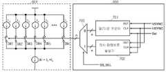
도 1은 종래 액정표시장치의 개략 블록도로서 이에 도시한 바와 같이, 복수개의 게이트 라인과 데이터 라인이 서로 수직한 방향으로 배열되어 매트릭스 형태의 픽셀영역을 갖는 액정패널(110); 상기 액정패널(110)에 구동 신호와 데이터 신호를 공급하는 구동회로부(121) 및, 상기 구동회로부(121)에서 필요로 하는 각종 전원을 공급하는 전원공급부(122)로 구성된 엘디아이(LDI: LCD Driver IC)(120)를 구비한다.1 is a schematic block diagram of a conventional liquid crystal display device, as shown in FIG. 1, wherein a plurality of gate lines and data lines are arranged in a direction perpendicular to each other and have a matrix-type pixel region; An LCD (LDI: LCD) including a
상기 구동회로부(121)는 게이트 드라이버(121A), 소스 드라이버(121B), 타이밍 콘트롤러(121C)를 구비한다.The
게이트 드라이버(121A)는 상기 액정패널(110)의 각 게이트 라인을 구동하기 위한 게이트 구동신호를 출력한다.The
소스 드라이버(121B)는 상기 액정패널(110)의 각 데이터 라인에 데이터 신호를 출력한다.The
타이밍 콘트롤러(121C)는 상기 게이트 드라이버(121A) 및 소스 드라이버(121B)의 구동을 제어함과 아울러, 전원공급부(122)의 구동을 제어한다.The
전원공급부(122)는 전원 제어부(122A), 소스전원 구동부(122B) 및 게이트전원 구동부(122C)를 구비한다.The
전원 제어부(122A)는 상기 타이밍 콘트롤러(121C)의 제어를 받아 소스전원 구동부(122B) 및 게이트전원 구동부(122C)의 구동을 제어한다.The
이때, 상기 게이트전원 구동부(122C)는 상기 게이트 드라이버(121A)에서 상기 게이트 구동신호를 생성하는데 필요로 하는 게이트 하이 전압(

그리고, 소스전원 구동부(122B)는 상기 소스 드라이버(121B)에서 상기 데이터 신호를 생성하는데 필요로 하는 정극성의 패널구동전압(이하, '패널구동전압'이라 칭함)(VDDP)과 부극성의 패널구동전압(VDDN)을 공급한다.In addition, the
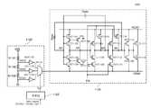
도 2는 상기 엘디아이(120)의 소스전원 구동부(122B)에 구비되어 패널구동전압(VDDP)을 출력하는 부스트 컨버터 회로도로서 이에 도시한 바와 같이, 스위칭펄스(LSW)에 따라 리액터(L1)를 구동하는 전계효과트랜지스터(FET1); 상기 전계효과트랜지스터(FET1)의 스위칭 동작에 의하여 상기 리액터(L1)로부터 역류방지용 다이오드(D1)를 통해 로딩되는 전압을 저장하는 콘덴서(Cout); 상기 콘덴서(Cout)에 저장된 후 출력되는 패널구동전압(VDDP)을 소정 레벨로 분압하는 저항(R1,R2); 상기 저항(R1,R2)에 의해 분압된 전압을 근거로 상기 패널구동전압(VDDP)을 모니터링하여 목적한 레벨로 출력되도록 상기 스위칭펄스(LSW)를 제어하는 제어부(200)로 구성된다.FIG. 2 is a boost converter circuit diagram provided in the
삭제delete
삭제delete
삭제delete
전계효과트랜지스터(FET1)는 제어부(200)로부터 입력되는 도 3의 (a)와 같은 스위칭펄스(LSW)에 의해 일련의 온오프 동작을 반복한다. 이때, 상기 전계효과트랜지스터(FET1)의 스위칭 동작에 의하여 상기 리액터(L1)로부터 로딩되는 부스팅전압은 역류방지용 다이오드(D1)를 통해 콘덴서(Cout)에 저장된다.The field effect transistor FET1 repeats a series of on / off operations by the switching pulse LSW as shown in FIG. 3A input from the
상기와 같은 경로를 통해 상기 콘덴서(Cout)에 저장된 부스팅전압이 상기 패널구동전압(VDDP)으로 출력된다.The boosting voltage stored in the capacitor Cout is output to the panel driving voltage VDDP through the path as described above.
그런데, 상기 패널구동전압(VDDP)의 출력단자를 통해 외부로 로딩되는 전류량이 상기 콘덴서(Cout)에 축적되는 전류량보다 적은 경우 그 패널구동전압(VDDP)이 불필요하게 높게 상승된다.However, when the amount of current loaded to the outside through the output terminal of the panel driving voltage VDDP is smaller than the amount of current stored in the capacitor Cout, the panel driving voltage VDDP is unnecessarily increased.
이를 방지하기 위하여, 저항(R1,R2)을 이용하여 상기 콘덴서(Cout)로부터 출력되는 패널구동전압(VDDP)을 소정 레벨로 분압하고, 제어부(200)는 그 분압된 전압을 근거로 패널구동전압(VDDP)을 모니터링하여 목적한 레벨로 출력되도록 상기 스위칭펄스(LSW)를 제어한다.In order to prevent this, the panel driving voltage VDDP output from the capacitor Cout is divided to a predetermined level by using the resistors R1 and R2, and the
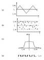
상기 스위칭펄스(LSW)의 예로써, PWM(Pulse-Width Modulation) 펄스와 PFM(Pulse Frequency Modulation) 펄스가 있다. 상기 PWM 펄스를 사용하는 경우 상기 제어부(200)는 그 PWM 펄스의 듀티비를 조절하여 목적한 레벨의 부스팅전압이 출력되도록 하고, PFM 펄스를 사용하는 경우에는 그 PFM 펄스의 주파수를 조절하여 목적한 레벨의 부스팅전압이 출력되도록 한다.Examples of the switching pulse LSW include pulse-width modulation (PWM) pulses and pulse frequency modulation (PFM) pulses. When the PWM pulse is used, the
일반적으로, 상기 제어부(200)는 출력하고자 하는 스위칭펄스(LSW)의 형태가 결정되면 이를 도 3의 (a)에서와 같이 동일 위상으로 출력한다. 따라서, 주기적인 부스팅 동작으로 인하여 스펙트럼이 도 3의 (b)에서와 같이 중심주파수(f0) 대역에 집중된다.In general, when the shape of the switching pulse LSW to be output is determined, the
이와 같이 종래의 LDI 시스템의 부스트 컨버터 회로에 있어서는 리액터 구동을 위한 스위칭 펄스로써 동일 위상의 스위칭펄스를 사용하여 주기적인 부스팅 동작에 의해 증폭된 형태의 에너지 스펙트럼이 형성되고, 이로 인하여 조화 주파수(harmonic frequency)의 에너지 스펙트럼도 증폭된 형태로 나타난다.As described above, in a boost converter circuit of a conventional LDI system, an energy spectrum amplified by a periodic boosting operation using a switching pulse of the same phase as a switching pulse for driving a reactor is formed, and thus a harmonic frequency. ) Is also shown in amplified form.
더욱이, 증폭된 형태의 에너지 스펙트럼은 시스템에 사용하는 다른 신호의 주파수에 대해서 전자파간섭(EMI: ElectroMagnetic Interference)을 유발시키는 문제점이 있었다.Moreover, the amplified energy spectrum has a problem of causing electromagnetic interference (EMI) for frequencies of other signals used in the system.
근래 들어, 이와 같은 문제점을 해소하기 위해 가변주파수 형태의 스위칭 펄스를 발생하여 스프레드 스펙트럼(spread spectrum)이 나타나도록 하고 있다. 그러나, 매 프레임이 시작될 때마다 서로 다른 주파수의 스위칭펄스를 사용하여 그 때마다 조금씩 다른 레벨의 패널구동전압이 출력되고, 이로 인하여 화상이 불안정하게 디스플레이되는 문제점이 있었다.Recently, in order to solve such a problem, a spread spectrum is generated by generating a switching pulse of a variable frequency type. However, there is a problem in that panel driving voltages of slightly different levels are output each time by using switching pulses of different frequencies at every start of the frame, thereby causing an image to be unstablely displayed.
따라서, 본 발명이 해결하고자 하는 과제는 엘디아이의 부스트 컨버터에서 가변주파수를 이용하여 패널구동전압을 생성하여 전자파 간섭이 저감되도록 하되, 매 프레임이 시작될 때 마다 동일한 주파수를 사용하여 부스팅 동작이 안정되게 이루어지도록 하는데 있다.Therefore, the problem to be solved by the present invention is to reduce the electromagnetic interference by generating a panel drive voltage using a variable frequency in the boost converter of the L-DAI, the boosting operation is stable using the same frequency every frame start To make it happen.
본 발명이 해결하고자 하는 과제들은 앞에서 언급한 과제들로 제한되지 않는다. 본 발명의 다른 과제 및 장점들은 아래 설명에 의해 더욱 분명하게 이해될 것이다.Problems to be solved by the present invention are not limited to the aforementioned problems. Other objects and advantages of the invention will be more clearly understood by the following description.
상기와 같은 과제를 달성하기 위한 본 발명은, 중심주파수를 기준으로 일정한 패턴으로 변화되거나 불규칙적으로 홉핑하는 주파수의 발진신호를 동기신호에 동기시켜 생성하고, 매 프레임이 시작될 때마다 미리 정해진 고정된 주파수의 발진신호를 생성하는 발진기; 상기 발진기에서 출력되는 발진신호, 패널구동전압에서 검출한 전압, 기 설정된 기준전압을 이용하여 요구되는 패널구동전압을 생성하기 위한 스위칭 신호를 출력하는 제어기; 상기 제어기에서 출력되는 스위칭 신호를 이용하여, 상기 패널구동전압을 발생하는 리액터를 구동하는 트랜지스터를 스위칭 동작시키는 드라이버;를 포함하는 부스트 컨버터를 제공하는데 있다.The present invention for achieving the above object is generated by synchronizing an oscillation signal of a frequency that is changed or irregularly hopping in a predetermined pattern on the basis of the center frequency in synchronization with a synchronization signal, a predetermined fixed frequency at each frame start An oscillator for generating an oscillation signal of the; A controller for outputting a switching signal for generating a required panel driving voltage using an oscillation signal output from the oscillator, a voltage detected from the panel driving voltage, and a preset reference voltage; And a driver for switching a transistor for driving a reactor for generating the panel driving voltage using the switching signal output from the controller.
삭제delete
삭제delete
삭제delete
본 발명은 엘디아이의 부스트 컨버터에서 가변주파수를 이용하여 패널구동전압을 생성하여 전자파 간섭이 저감되도록 하고, 매 프레임이 시작될 때 마다 동일한 주파수를 사용하여 부스팅 동작이 화상에 영향을 주지 않고 안정되게 수행할 수 있는 효과가 있다.The present invention generates a panel driving voltage using a variable frequency in the LDL's boost converter to reduce electromagnetic interference, and the boosting operation is stably performed without affecting the image by using the same frequency at the beginning of each frame. It can work.
도 1은 종래 액정표시장치의 개략 블록도.
도 2는 엘디아이에 구비되는 부스트 컨버터 회로도.
도 3의 (a)는 스위칭펄스의 파형도.
도 3의 (b)는 종래의 부스팅 동작에 의한 스펙트럼.
도 4는 본 발명에 의한 액정표시장치의 부스트 컨버터의 블록도.
도 5의 (a)는 본 발명에 의해 주파수가 일정한 패턴으로 변화되는 것을 나타낸 그래프.
도 5의 (b)는 본 발명에 의해 주파수가 랜덤한 패턴으로 변화되는 것을 나타낸 그래프.
도 5의 (c)는 본 발명에 의해 주파수가 가변되어 에너지가 스프레드된 스펙트럼을 나타낸 그래프.
도 5의 (d)는 본 발명에 의해 주파수가 가변되어 나타난 스위칭 펄스의 파형도.
도 6은 발진기의 제1실시예를 나타낸 회로도.
도 7은 도 6에서 전류원 및 카운터의 상세 블록도.
도 8의 (a)-(g)는 도 7 각부의 파형도.
도 8의 (h)는 본 발명에 적용된 수직동기신호의 파형도.
도 8의 (i)는 본 발명에서, 수직동기신호 및 수평동기신호에 의해 결정되는 카운터의 출력값 변화를 나타낸 설명도.
도 9는 도 7에서 업/다운카운터의 상세 회로도.
도 10은 도 7에서 의사 랜덤비트 발생기의 상세 회로도.
도 11은 발진기의 제2실시예를 나타낸 회로도.
도 12의 (a)-(d)는 도 11 각부의 파형도.
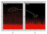
도 13의 (a)는 본 발명이 적용되지 않은 부스트 컨버터회로에서 발생되는 전자파 간섭(EMI)을 나타낸 도면.
도 13의 (b)는 본 발명에 의한 부스트 컨버터 회로에서 전자파 간섭이 저감된 것을 나타낸 실험 결과를 나타낸 도면.
도 14의 (a),(b)는 t1,t2의 같은 위상에서 동일한 패널구동전압으로 패널 구동이 가능하게 되는 것을 나타낸 파형도.1 is a schematic block diagram of a conventional liquid crystal display device.
Figure 2 is a boost converter circuit diagram provided in the ELDAI.
3A is a waveform diagram of a switching pulse.
Figure 3 (b) is a spectrum by a conventional boosting operation.
4 is a block diagram of a boost converter of a liquid crystal display according to the present invention;
Figure 5 (a) is a graph showing that the frequency is changed in a pattern by the present invention.
Figure 5 (b) is a graph showing that the frequency is changed in a random pattern by the present invention.
Figure 5 (c) is a graph showing a spectrum of energy spread by varying the frequency according to the present invention.
Figure 5 (d) is a waveform diagram of a switching pulse shown by varying the frequency in accordance with the present invention.
6 is a circuit diagram showing a first embodiment of an oscillator.
7 is a detailed block diagram of the current source and counter in FIG.
(A)-(g) is a waveform diagram of each part of FIG.
Figure 8 (h) is a waveform diagram of a vertical synchronization signal applied to the present invention.
8 (i) is an explanatory diagram showing a change in the output value of the counter determined by the vertical synchronization signal and the horizontal synchronization signal in the present invention.
FIG. 9 is a detailed circuit diagram of an up / down counter in FIG. 7. FIG.
FIG. 10 is a detailed circuit diagram of the pseudo random bit generator in FIG. 7. FIG.
Fig. 11 is a circuit diagram showing a second embodiment of the oscillator.
(A)-(d) is a waveform diagram of each part of FIG.
13A is a diagram showing electromagnetic interference (EMI) generated in a boost converter circuit to which the present invention is not applied.
Figure 13 (b) is a view showing the experimental results showing that electromagnetic interference is reduced in the boost converter circuit according to the present invention.
14A and 14B are waveform diagrams showing that the panel can be driven with the same panel driving voltage at the same phase of t1 and t2.
이하, 첨부한 도면을 참조하여 본 발명의 바람직한 실시예를 상세히 설명하면 다음과 같다.Hereinafter, exemplary embodiments of the present invention will be described in detail with reference to the accompanying drawings.
도 4는 본 발명에 의한 액정표시장치의 부스트 컨버터의 블록도로서 이에 도시한 바와 같이, 전계효과트랜지스터(FET1)로써 리액터(L1)를 구동하여 패널구동전압(VDDP)을 생성하는 부스트 컨버터에 있어서, 발진기(410); 패널구동전압 모니터링부(420); 온타임 카운터(430); 오프타임 카운터(440); SR 래치(450) 및, 드라이버(460)로 구성된 제어부(400)를 구비한다.FIG. 4 is a block diagram of a boost converter of a liquid crystal display according to the present invention. As shown in the drawing, in a boost converter for driving a reactor L1 with a field effect transistor FET1 to generate a panel driving voltage VDDP. ,
발진기(410)는 도 5의 (a)와 같이 중심주파수(

패널구동전압 모니터링부(420)는 반전입력단자에 기준전압(Vref)이 공급되고 반전입력단자가 패널구동전압(VDDP)의 단자에 직렬접속된 저항(R1,R2)의 접속점에 접속된 비교기(CP401), 반전입력단자에 기준전압(SSref)이 공급되고 비반전입력단자가 상기 저항(R1,R2)의 접속점에 접속된 비교기(CP402) 및, 일측 입력단자가 오프타임카운터(440)의 출력단자에 접속되고, 타측 단자가 상기 비교기(CP401)의 출력단자에 접속된 앤드게이트(AD401)를 구비한다.
비교기(CP401)는 저항(R1,R2)에 의해 분배된 패널구동전압(VDDP)을 기준전압(Vref)과 비교하여 그에 따른 신호를 출력한다. 비교기(CP402)는 상기 저항(R1,R2)에 의해 분배된 패널구동전압(VDDP)을 소프트 스타트를 위해 설정된 기준전압(SSref)과 비교하여 그에 따른 모니터링신호를 출력한다. 앤드게이트(AD401)는 상기 비교기(CP401)의 출력신호와 오프타임 카운터(440)의 출력신호를 앤드연산하여 그에 따른 모니터링신호를 출력한다.The panel driving
The comparator CP401 compares the panel driving voltage VDDP distributed by the resistors R1 and R2 with the reference voltage Vref and outputs a signal accordingly. The comparator CP402 compares the panel driving voltage VDDP distributed by the resistors R1 and R2 with a reference voltage SSref set for soft start and outputs a monitoring signal accordingly. The AND gate AD401 performs an AND operation on the output signal of the comparator CP401 and the output signal of the off-
온타임 카운터(430)는 수직동기신호(Vsync)에 의해 리세트된 후 상기 발진기(410)에서 출력되는 발진신호의 온타임 구간을 카운트한다.The on
오프타임 카운터(440)는 수직동기신호(Vsync)에 의해 리세트된 후 상기 발진기(410)에서 출력되는 발진신호의 오프타임 구간을 카운트한다.The
SR 래치(450)는 상기 앤드게이트(AD401)에서 출력되는 모니터링신호를 세트단자(S)로 입력받고, 상기 온타임 카운터(430)에서 출력되는 신호를 리세트단자(R)로 입력받아 에러가 정정된 스위칭펄스(LSW) 형태의 펄스를 출력한다.The
드라이버(460)는 상기 SR 래치(450)로부터 입력되는 펄스를 전계효과트랜지스터(FET1)를 스위칭하는데 적당한 형태의 스위칭펄스(LSW)로 변환하여 출력한다. 상기 드라이버(460)에서 출력되는 스위칭펄스(LSW)는 상기 도 5의 (d)에서와 같이 가변주파수 형태를 갖는다.The
전계효과트랜지스터(FET1)는 상기 드라이버(460)로부터 입력되는 상기 스위칭펄스(LSW)에 의해 일련의 온오프 동작을 반복한다. 이때, 상기 전계효과트랜지스터(FET1)의 스위칭 동작에 의하여 상기 리액터(L1)로부터 로딩되는 부스팅전압은 역류방지용 다이오드(D1)를 통해 콘덴서(Cout)에 저장된다.The field effect transistor FET1 repeats a series of on / off operations by the switching pulse LSW input from the
상기와 같은 경로를 통해 상기 콘덴서(Cout)에 저장된 부스팅전압이 패널구동전압(VDDP)으로 출력된다.The boosting voltage stored in the capacitor Cout is output as the panel driving voltage VDDP through the path as described above.
도 6은 상기와 같이 동작하는 발진기(410)의 제1실시예를 나타낸 회로도로서 이에 도시한 바와 같이, 가변전류를 출력하는 제1,2전류원(601),(602); 동기신호를 카운트하여 상기 카운트값을 근거로 상기 제1,2전류원(601),(602)의 출력전류를 가변하는 카운터(603); 상기 제1전류원(601)의 출력전류에 상응되게 충전전압을 변경하고, 상기 변경되는 충전전압을 제1기준전압과 비교하여 상기 비교결과에 따른 세트신호를 생성하는 세트신호 출력부(604); 상기 제2전류원(602)의 출력전류에 상응되게 충전전압을 변경하고, 상기 변경되는 충전전압을 제2기준전압과 비교하여 상기 비교 결과 따른 리세트신호를 생성하는 리세트신호 출력부(605); 상기 세트신호 출력 부(604)에서 출력되는 세트신호와 상기 리세트신호 출력부(605)에서 출력되는 리세트신호에 따라 구형파 형태의 출력신호 및 반전출력신호를 생성하고, 상기 구형파 형태의 출력신호 및 반전출력신호를 근거로 하여 상기 제1전류원(601) 및 제2전류원(602)의 출력전류를 제어하는 SR 래치(606)를 구비한다.
제1,2전류원(601),(602), 카운터(603), 세트신호 출력부(604), 리세트신호 출력부(605), SR 래치(606)를 구비한다.6 is a circuit diagram showing a first embodiment of the
First and second
SR 래치(606)의 세트단자(S), 리세트단자(R)에 '로우','하이'가 입력될 때 출력단자(Q),(Qb)에 '로우','하이'가 출력된다. 이에 따라, 세트신호 출력부(604)의 트랜지스터(FET601)가 턴온되는 반면, 트랜지스터(FET602)는 턴오프된다. 이때, 리세트신호 출력부(605)의 트랜지스터(FET603)가 턴오프되는 반면, 트랜지스터(FET604)는 턴온된다.When 'low' and 'high' are input to the set terminal S and the reset terminal R of the
이에 따라, 제1전류원(601)으로부터 공급되는 전압이 상기 트랜지스터(FET601)를 통해 콘덴서(C601)에 충전된다. 비교기(CP601)는 제1입력단자에 입력되는 상기 콘덴서(C601)의 충전전압을 기준전압과 비교하여 그 충전전압이 기준전압을 상회하는 순간 상기 SR 래치(606)의 세트단자(S)에 '하이'를 출력한다. 이때, 상기 콘덴서(C602)의 충전전압은 상기 트랜지스터(FET604)를 통해 접지단자로 방전된다. 그러므로, 비교기(CP602)의 제1입력단자에 '로우'가 입력되어 이의 출력단자로부터 상기 SR 래치(606)의 리세트단자(R)에 '로우'가 출력된다. 따라서, 상기 SR 래치(606)의 출력단자(Q),(Qb)에 '하이','로우'가 출력된다.Accordingly, the voltage supplied from the first
이후, 상기 SR 래치(606)의 출력단자(Q),(Qb)에서 출력되는 '하이','로우'에 의해 상기 세트신호 출력부(604)의 트랜지스터(FET601)가 턴오프되는 반면, 트랜지스터(FET602)는 턴온된다. 이때, 리세트신호 출력부(605)의 트랜지스터(FET603)는 턴온되는 반면, 트랜지스터(FET604)는 턴오프된다.Thereafter, the transistor FET601 of the set
이에 따라, 상기와 같은 과정을 통해 SR 래치(606)의 세트단자(S), 리세트단자(R)에 '로우','하이'가 입력된다. 따라서, 상기 SR 래치(606)의 출력단자(Q),(Qb)에 '로우','하이'가 출력된다.Accordingly, 'low' and 'high' are input to the set terminal S and the reset terminal R of the
결국, 상기와 같이 동작하는 리세트신호 출력부(604)와 세트신호 출력부(605)에 의해 상기 SR 래치(606)의 세트단자(S)에 '하이', '로우'가 교번되게 입력되고, 이에 의해 그의 출력단자(Q)에 해당 주파수의 구형파가 출력된다.As a result, 'high' and 'low' are alternately inputted to the set terminal S of the
그런데, 카운터(603)는 각종 동기신호(예: Vsync, Hsync, DE 등)에 동기하여 상기 제1,2전류원(601),(602)의 출력 전류량을 제어하여 상기 콘덴서(C601),(C602)의 충전 시간을 가변시키고, 이에 의해 상기 SR 래치(606)의 출력단자(Q)에 출력되는 구형파의 주파수가 가변되어 스프레드 스펙트럼이 구현된다. 따라서, 전자파 간섭이 저감된다.However, the
도 7은 상기 제1전류원(601) 및 카운터(603)의 구현예를 나타낸 것이다. 상기 제1전류원(601)과 제2전류원(602)은 서로 동일 구성이므로 도 7에서는 그 중에서 하나의 제1전류원(601)을 예시적으로 나타내었다. 제1전류원(601)은 스위치(SW1-SWn)에 각기 직렬접속되고 서로 병렬접속된 다수의 전류원(I1-In)을 각기 구비한다. 그리고, 상기 카운터(603)는 업/다운카운터(701), 의사 랜덤비트 발생기(PRBG: Pseudo Random Bit Generator)(702) 및, 상기 업/다운 카운터(701)의 출력신호나 의사 랜덤비트 발생기(702)의 출력신호를 선택하여 상기 스위치(SW1-SWn)의 스위칭 동작을 제어하는 멀티플렉서(703)를 구비한다.7 illustrates an embodiment of the first
제1전류원(601)은 스위치(SW1-SWn)에 각기 직렬접속되고 서로 병렬접속된 다수의 전류원(I1-In)을 각기 구비하는데, 상기 스위치(SW1-SWn)는 카운터(603)에서 출력되는 n 비트의 스위칭제어신호에 의해 턴온되어 그에 따른 가변전류를 출력한다. 예를 들어, 상기 스위치(SW1-SWn) 중에서 상기 스위칭 제어신호에 의해 스위치(SW2,SW4)가 턴온되는 경우 상기 제1,2전류원(601,602)에서 △I = I2 + I4의 가변전류가 출력된다.The first
상기 업/다운카운터(701)의 출력신호 및 의사 랜덤비트 발생기(702)의 출력신호는 멀티플렉서(703)에서 선택신호(SS_SEL)에 의해 선택되어 상기 제1,2전류원(601,602)의 스위치(SW1-SWn)에 전달된다.The output signal of the up / down
상기 업/다운카운터(701)는 도 8의 (a),(d)와 같이 매 프레임의 첫 번째 수평라인을 구동할 때 마다 수직동기신호(Vsync)에 의해 리세트되어 n 비트의 스위칭제어신호를 기 설정된 값으로 출력하고, 이에 의해 상기 제1,2전류원(601,602)의 스위치(SW1-SWn) 중에서 해당 스위치들이 턴온되어 그에 따른 전류량이 출력된다. 따라서, 상기 SR 래치(606)의 출력단자(Q)에서 해당 주파수 예를 들어, 도 8의 (e)에서와 같이 8MHz의 발진주파수가 출력된다.The up / down
이후, 상기 업/다운카운터(701)는 도 8의 (b),(c)에서와 같은 수평동기신호(Hsync)나 데이터인에이블신호(DE)를 도 8의 (d)에서와 같이 일정한 패턴으로 업/다운 카운트하여 그에 따른 n 비트의 스위칭제어신호를 출력한다. 이에 따라 상기 SR 래치(606)의 출력단자(Q)에서 도 8의 (e)와 같이 주기적으로 변화되는 상기 n 비트의 가변주파수의 신호가 출력된다.Thereafter, the up / down
또한, 의사 랜덤비트 발생기(702)는 도 8의 (a),(f)와 같이 매 프레임의 첫 번째 수평라인을 구동할 때 마다 수직동기신호(Vsync)에 의해 리세트되어 n 비트의 스위칭제어신호를 기 설정된 값으로 출력하고, 이에 의해 상기 제1,2전류원(601,602)의 스위치(SW1-SWn) 중에서 해당 스위치들이 턴온되어 그에 따른 전류량이 출력된다. 따라서, 상기 SR 래치(606)의 출력단자(Q)에서 해당 주파수 예를 들어, 도 8의 (g)에서와 같이 8MHz의 발진주파수가 출력된다.In addition, the pseudo
이와 같이 매 프레임이 시작될 때마다 동일한 주파수의 발진신호가 출력되게 함으로써, 가변주파수를 이용하여 전자파 간섭을 저감시킬 때 화상에 영향을 주지 않고 안정된 부스팅 동작을 보장할 수 있게 된다.In this way, the oscillation signal of the same frequency is output every time the frame is started, thereby ensuring stable boosting operation without affecting the image when reducing the electromagnetic interference by using the variable frequency.
이후, 상기 의사 랜덤비트 발생기(702)는 도 8의 (b),(c)에서와 같은 수평동기신호(Hsync)나 데이터인에이블신호(DE)를 도 8의 (f)에서와 같이 불규칙한 패턴으로 업/다운 카운트하여 그에 따른 n 비트의 스위칭제어신호를 출력한다. 이에 따라 상기 SR 래치(606)의 출력단자(Q)에서 도 8의 (g)와 같이 불규칙적으로 변화되는 상기 n 비트의 가변주파수의 신호가 출력된다.Thereafter, the pseudo
상기 도 7에서, 선택신호(Sel)는 상기 업/다운카운터(701)의 업카운팅이나 다운카운팅 동작을 선택하고, 상기 의사 랜덤비트 발생기(702)의 랜덤비트 발생주기를 선택한다. 도 8의 (h),(i)는 상기 선택신호(Sel)를 이용하여,In FIG. 7, the selection signal Sel selects an up counting or down counting operation of the up / down
수직동기신호(Vsync)나 수평동기신호(Hsync)가 입력될 때마다, 또는 임의의 수직동기신호(Vsync)나 수평동기신호(Hsync)가 입력될 때마다 상기 업/다운카운터(701) 또는 의사 랜덤비트 발생기(702)의 카운트 주기를 변화시키는 예를 나타낸 것이다. 이렇게 함으로써, 상기 업/다운카운터(701) 또는 의사 랜덤비트 발생기(702)가 수직동기신호(Vsync)나 수평동기신호(Hsync)가 입력될 때마다, 또는 임의의 수직동기신호(Vsync)나 수평동기신호(Hsync)가 입력될 때마다 카운트값을 변경하여 부스트 컨버터에 의해 발생하는 에너지 스펙트럼이 분산된다. 이에 따라, 에너지 상승으로 인한 전자파 간섭을 저하시킬 수 있게 된다.Whenever the vertical sync signal Vsync or the horizontal sync signal Hsync is input, or whenever any vertical sync signal Vsync or the horizontal sync signal Hsync is input, the up / down counter 701 or the pseudo An example of changing the count period of the
도 9는 상기 업/다운카운터(701)의 구현예를 나타낸 회로도로서 이에 도시한 바와 같이, 클럭신호단자가 수평동기신호 단자(Hsync)에 공통으로 접속되고, 클리어단자(CLR)가 수직동기신호 단자(Vsync)에 공통으로 접속된 N 단의 T형 플립플롭(F/F901A-F/F901N); 선택신호(SEL)를 반전출력하는 인버터(I901), 제1,2입력단자가 상기 선택신호단자(SEL), T형 플립플롭(F/F901A)의 출력단자(Q1)에 각기 접속된 앤드게이트(AD901), 제1,2입력단자가 상기 T형 플립플롭(F/F901A)의 반전출력단자(Qb1), 상기 인버터(I901)의 출력단자에 각기 접속된 앤드게이트(AD902), 제1,2입력단자가 상기 앤드게이트(AD901),(AD902)의 출력단자에 각기 접속된 오아게이트(OR901)로 구성된 제1출력신호 연산부(901A); 제1,2입력단자가 상기 앤드게이트(AD901)의 출력단자, T형 플립플롭(F/F901B)의 출력단자(Q2)에 각기 접속된 앤드게이트(AD903), 제1,2입력단자가 상기 T형 플립플롭(F/F901B)의 반전출력단자(Qb2), 상기 앤드게이트(AD902)의 출력단자에 각기 접속된 앤드게이트(AD904), 제1,2입력단자가 상기 앤드게이트(AD903),(AD904)의 출력단자에 각기 접속된 오아게이트(OR902)로 구성된 제2출력신호 연산부(901B); 상기 제2출력신호 연산부(901B)의 이후 단에 상기 출력신호 연산부(901B)와 같이 구성된 제3-N출력신호 연산부(901C)-(901N)를 구비한다. FIG. 9 is a circuit diagram illustrating an implementation example of the up / down
삭제delete
삭제delete
삭제delete
도 10은 상기 의사 랜덤비트 발생기(702)의 구현예를 나타낸 회로도로서 이에 도시한 바와 같이, 클럭신호단자가 수평동기신호 단자(Hsync)에 공통으로 접속되고, 클리어단자(CLR)가 수직동기신호 단자(Vsync)에 공통으로 접속된 N 단의 D형 플립플롭(F/F1001A-F/F1001N); 선택신호(SEL)에 따라 상기 D형 플립플롭(F/F1001A-F/F1001N)의 출력단자(Q1-Qn)의 출력신호를 선택하여 출력하는 멀티플렉서(MUX1001); 상기 멀티플렉서(MUX1001)의 출력신호를 익스클루시브 오아 연산하여 그 연산결과를 상기 첫 번째 단의 D형 플립플롭(F/F1001A)의 입력단자(D)로 피드백하는 익스클루시브오아 게이트(XOR1001)를 구비한다.FIG. 10 is a circuit diagram illustrating an implementation of the pseudo
삭제delete
삭제delete
도 11은 상기 도 4에서 발진기(410)의 제2실시예를 나타낸 회로도로서 이에 도시한 바와 같이, RC 발진회로(1101), 그라운드전압 발생부(1102), 카운터(1103)을 구비한다.FIG. 11 is a circuit diagram illustrating a second embodiment of the
제1노드(N1)와 제3노드(N3)는 콘덴서(Cosc)에 의해 연결되어 있다. 따라서, 제3노드(N3)가 '하이'이면 제1노드(N1)는 그에 상응되는 레벨로 부스팅된다.The first node N1 and the third node N3 are connected by a capacitor Cosc. Therefore, when the third node N3 is 'high', the first node N1 is boosted to a level corresponding thereto.
상기 제3노드(N3)가 '하이'이면 이에 의해 트랜지스터(FET111)가 턴오프되는 반면, 트랜지스터(FET1112),(FET1113)가 턴온되므로, 제4노드(N4)는 그라운드전압(VSSA)의 레벨로 된다. 따라서, RC 시정수(Rosc?Cosc)로 충전된 상기 콘덴서(Cosc)의 전하가 상기 제4노드(N4)로 방전된다.When the third node N3 is 'high', the transistor FET111 is turned off, whereas the transistors FET1112 and FET1113 are turned on, so that the fourth node N4 is at the level of the ground voltage VSSA. It becomes Therefore, the charge of the capacitor Cosc charged with the RC time constant Rosc? Cosc is discharged to the fourth node N4.
후술하는 바와 같이 상기 그라운드전압(VSSA)은 그라운드전압 발생부(1102), 카운터(1103)에 의하여 VSSA1, VSSA2, VSSA3 레벨의 그라운드전압으로 가변되는데, 도 12의 (a)에서와 같이 제1노드(N1) 전압이 로직 드레쉬홀드전압을 넘으면(떨어지면) 제2노드(N2)의 전압은 상승되고, 제3노드(N3)의 전압은 하강된다. 이때, 제4노드(N4)는 '하이'이므로 RC 시정수로 상기 콘덴서(Cosc)가 충전된다.As described later, the ground voltage VSSA is changed to ground voltages of VSSA1, VSSA2, and VSSA3 levels by the
이와 같은 동작이 반복 수행되면서 RC 발진 동작이 이루어진다. 이때의 발진주파수는 트랜지스터의 온저항을 무시하면 RC 타임의 두배 주기로 발진한다.As such an operation is repeatedly performed, an RC oscillation operation is performed. At this time, the oscillation frequency oscillates at twice the RC time, ignoring the on resistance of the transistor.
그런데, 상기와 같은 RC 발진회로(1101)를 사용하여 원하는 주파수의 신호를 생성할 때, 아래의 설명에서와 같이 그라운드전압(VSSA)을 가변하여 스프레드 스펙트럼이 구현되도록 하였다.By the way, when generating a signal of the desired frequency using the
즉, 그라운드 전원전압(VSS)을 분배용 직렬저항(R1101),(R1102),(R1103)을 이용하여 VSSA1, VSSA2,VSSA3의 레벨로 분압하고 버퍼(BUF1101),(BUF1102),(BUF103)를 통해 버퍼링한 후 멀티플렉서(MUX1101)를 통해 그 중에서 하나를 선택하여 RC 발진회로의 그라운드전압(VSSA)으로 출력한다. 이때, 카운터(1103)를 이용하여 상기 멀티플렉서(MUX1101)에서의 그라운드전압 선택동작을 제어함으로써, RC 발진회로의 발진주파수를 가변시킬 수 있게 되는데, 도 12의 (a)-(d)는 이에 의해 제1-4노드(N1-N4)의 위상이 변화되는 예를 나타낸 파형도이다.That is, the ground power supply voltage VSS is divided into levels of VSSA1, VSSA2, and VSSA3 using the series resistors R1101, R1102, and R1103 for distribution, and the buffers BUF1101, BUF1102, and BUF103 are divided. After buffering through, select one of them through the multiplexer (MUX1101) and output it to the ground voltage (VSSA) of the RC oscillator circuit. At this time, by controlling the ground voltage selection operation of the multiplexer MUX1101 using the
이를 위해 상기 카운터(1103)를 다양하게 구현할 수 있는데, 예를 들어 상기 도 7에서와 같이 업/다운 카운터와 의사 랜덤비트 발생기를 구비하여 상기 설명에서와 같이 각종 동기신호(예: Vsync, Hsync, DE 등)에 동기하여 구동시킬 수 있다. 이에 의해 RC 발진회로(1101)에서 생성되는 발진신호의 주파수가 가변되어 스프레드 스펙트럼이 구현된다. 따라서, 화상에 영향을 주지 않는 안정된 부스팅 동작을 보장하면서 전자파 간섭을 저감할 수 있게 된다.To this end, the
도 13의 (a)는 본 발명이 적용되지 않은 부스트 컨버터회로에서 발생되는 전자파 간섭(EMI)을 나타낸 실험결과의 도면이고, 도 13의 (b)는 본 발명에 의한 부스트 컨버터 회로에서 전자파 간섭이 저감된 것을 나타낸 실험 결과의 도면이다.FIG. 13 (a) is a diagram of an experimental result showing electromagnetic interference (EMI) generated in a boost converter circuit to which the present invention is not applied. FIG. 13 (b) shows electromagnetic interference in a boost converter circuit according to the present invention. It is a figure of the experimental result which showed that it was reduced.
도 14의 (a),(b)는 본 발명에 따라 프레임이 시작될 때 마다 동기신호를 이용하여 동일한 패널구동전압으로 패널 구동이 가능하게 되는 것을 나타낸 파형도이다. 참고로, 상기 도 14의 (a)는 수직동기신호(Vsync)나 수평동기신호(Hsync) 또는 데이터인에이블신호(DE)의 파형도이고, 도 14의 (b)는 정,부패널구동전압(VDDP,VDDN)의 파형도이다.14A and 14B are waveform diagrams showing that the panel can be driven with the same panel driving voltage by using a synchronization signal every time a frame is started according to the present invention. For reference, FIG. 14A is a waveform diagram of a vertical sync signal Vsync, a horizontal sync signal Hsync, or a data enable signal DE, and FIG. 14B is a positive and negative panel driving voltage. This is a waveform diagram of (VDDP, VDDN).
이상에서 본 발명의 바람직한 실시예에 대하여 상세히 설명하였지만, 본 발명의 권리범위가 이에 한정되는 것이 아니라 다음의 청구범위에서 정의하는 본 발명의 기본 개념을 바탕으로 보다 다양한 실시예로 구현될 수 있으며, 이러한 실시예들 또한 본 발명의 권리범위에 속하는 것이다.
Although the preferred embodiment of the present invention has been described in detail above, the scope of the present invention is not limited thereto, and may be implemented in various embodiments based on the basic concept of the present invention defined in the following claims. Such embodiments are also within the scope of the present invention.
400 : 제어부
410 : 발진기
420 : 패널구동전압 모니터링부
430 : 온타임 카운터
440 : 오프타임 카운터
450 : SR 래치
460 : 드라이버400:
410 oscillator
420: panel driving voltage monitoring unit
430: On Time Counter
440: Off Time Counter
450: SR latch
460 driver
Claims (10)
Translated fromKorean중심주파수를 기준으로 일정한 패턴으로 변화되거나 불규칙적으로 홉핑하는 주파수의 발진신호를 생성하고, 매 프레임이 시작될 때마다 미리 정해진 고정된 주파수의 발진신호를 생성하는 발진기;
상기 발진기에서 출력되는 발진신호, 상기 패널구동전압에서 검출한 전압, 기 설정된 기준전압을 이용하여 요구되는 패널구동전압을 생성하기 위한 스위칭 신호를 출력하는 제어기;
상기 제어기에서 출력되는 스위칭 신호를 이용하여, 상기 패널구동전압을 발생하는 리액터를 구동하는 트랜지스터를 스위칭 동작시키는 드라이버;를 포함하되,
상기 발진기는,
가변전류를 출력하는 제1전류원 및 제2전류원;
동기신호를 카운트하고 그 카운트값을 이용하여 상기 제1전류원 및 제2전류원의 출력전류를 가변하는 카운터;
상기 제1전류원의 출력전류에 상응되게 충전전압을 변경하고, 상기 변경되는 충전전압을 제1기준전압과 비교하여 그에 따른 세트신호를 생성하는 세트신호 출력부;
상기 제2전류원의 출력전류에 상응되게 충전전압을 변경하고, 상기 변경되는 충전전압을 제2기준전압과 비교하여 그에 따른 리세트신호를 생성하는 리세트신호 출력부;
상기 세트신호 출력부에서 출력되는 세트신호와 상기 리세트신호 출력부에서 출력되는 리세트신호에 따라 구형파 형태의 출력신호 및 반전출력신호를 생성하고, 상기 출력신호 및 반전출력신호를 근거로 하여 상기 제1전류원 및 제2전류원의 출력전류를 제어하는 래치;를 포함하여 구성한 것을 특징으로 하는 액정표시장치의 부스트 컨버터.
In a boost converter of a liquid crystal display device in which a reactor is driven by a transistor that switches by a switching pulse to generate a panel driving voltage.
An oscillator for generating an oscillation signal of a frequency that is changed or irregularly hopped in a predetermined pattern based on the center frequency, and generating an oscillation signal of a predetermined fixed frequency at each frame start;
A controller for outputting a switching signal for generating a required panel driving voltage using an oscillation signal output from the oscillator, a voltage detected by the panel driving voltage, and a preset reference voltage;
And a driver for switching the transistor for driving the reactor for generating the panel driving voltage using the switching signal output from the controller.
The oscillator,
A first current source and a second current source for outputting a variable current;
A counter for counting a synchronization signal and varying output currents of the first current source and the second current source using the count value;
A set signal output unit configured to change a charging voltage corresponding to the output current of the first current source, and compare the changed charging voltage with a first reference voltage to generate a set signal according thereto;
A reset signal output unit for changing a charging voltage corresponding to the output current of the second current source, and comparing the changed charging voltage with a second reference voltage to generate a reset signal according thereto;
A square wave output signal and an inverted output signal are generated according to the set signal output from the set signal output unit and the reset signal output from the reset signal output unit, and generated based on the output signal and the inverted output signal. And a latch for controlling output currents of the first current source and the second current source.
상기 카운터에 의해 제어되는 다수의 스위치;
상기 다수의 스위치 중 하나와 직렬접속되고 서로 병렬접속된 다수의 전류원을 각기 구비한 것을 특징으로 하는 액정표시장치의 부스트 컨버터.
The method of claim 1, wherein the first current source and the second current source is
A plurality of switches controlled by the counter;
And a plurality of current sources connected in series with one of the plurality of switches and connected in parallel with each other.
매 프레임이 시작될 때마다 수직동기신호에 의해 리세트되어 n 비트의 스위칭제어신호를 기 설정된 값으로 출력한 후 수평동기신호나 데이터인에이블신호를 일정한 패턴으로 업/다운 카운트하여 그에 따른 n 비트의 스위칭제어신호를 출력하는 업/다운카운터;
매 프레임이 시작될 때 마다 수직동기신호에 의해 리세트되어 n 비트의 스위칭제어신호를 기 설정된 값으로 출력한 후 수평동기신호나 데이터인에이블신호에 의해 불규칙한 패턴으로 업/다운 카운트하여 그에 따른 n 비트의 스위칭제어신호를 출력하는 의사 랜덤비트 발생기;
선택신호에 따라 상기 업/다운카운터의 출력신호나 의사 랜덤비트 발생기의 출력신호를 선택하여 출력하는 멀티플렉서를 포함하여 구성된 것을 특징으로 하는 액정표시장치의 부스트 컨버터.
The method of claim 1, wherein the counter
Each time the frame starts, it is reset by the vertical synchronization signal and outputs n-bit switching control signal to the preset value. Then, the horizontal synchronization signal or data enable signal is up / down counted in a predetermined pattern and the n-bit An up / down counter for outputting a switching control signal;
Each time the frame starts, it is reset by the vertical synchronization signal and outputs the n-bit switching control signal to the preset value, and then up / down counts in an irregular pattern by the horizontal synchronization signal or the data enable signal. A pseudo random bit generator for outputting a switching control signal of the pseudo random bit generator;
And a multiplexer for selecting and outputting an output signal of the up / down counter or an output signal of a pseudo random bit generator according to a selection signal.
The boost converter of claim 4, wherein the up / down counter is configured to determine an up / down count operation by a selection signal.
The boost converter of claim 4, wherein a pseudo random bit generator has a random bit generation period determined by the selection signal.
중심주파수를 기준으로 일정한 패턴으로 변화되거나 불규칙적으로 홉핑하는 주파수의 발진신호를 생성하고, 매 프레임이 시작될 때마다 미리 정해진 고정된 주파수의 발진신호를 생성하는 발진기;
상기 발진기에서 출력되는 발진신호, 상기 패널구동전압에서 검출한 전압, 기 설정된 기준전압을 이용하여 요구되는 패널구동전압을 생성하기 위한 스위칭 신호를 출력하는 제어기;
상기 제어기에서 출력되는 스위칭 신호를 이용하여, 상기 패널구동전압을 발생하는 리액터를 구동하는 트랜지스터를 스위칭 동작시키는 드라이버;를 포함하되,
상기 발진기는,
그라운드전압의 변화에 따라 가변되는 주파수의 신호를 발진하는 RC 발진회로;
그라운드 전압을 각기 다른 몇개의 레벨로 분압하여 이들을 선택적으로 출력하는 그라운드전압 발생부;
동기신호에 동기하여 상기 그라운드전압 발생부에서의 그라운드전압 선택동작을 제어하는 카운터;를 포함하여 구성된 것을 특징으로 하는 액정표시장치의 부스트 컨버터.
In a boost converter of a liquid crystal display device in which a reactor is driven by a transistor that switches by a switching pulse to generate a panel driving voltage.
An oscillator for generating an oscillation signal of a frequency that is changed or irregularly hopped in a predetermined pattern based on the center frequency, and generating an oscillation signal of a predetermined fixed frequency at each frame start;
A controller for outputting a switching signal for generating a required panel driving voltage using an oscillation signal output from the oscillator, a voltage detected by the panel driving voltage, and a preset reference voltage;
And a driver for switching the transistor for driving the reactor for generating the panel driving voltage using the switching signal output from the controller.
The oscillator,
An RC oscillation circuit oscillating a signal having a frequency varying with a change in ground voltage;
A ground voltage generator for dividing the ground voltage into several different levels and selectively outputting the ground voltages;
And a counter for controlling a ground voltage selection operation of the ground voltage generator in synchronization with a synchronous signal.
그라운드전압 VSSA를 VSSA1, VSSA2, VSSA3 레벨의 그라운드전압으로 분압하는 직렬접속저항;
상기 분압된 그라운드전압 VSSA1, VSSA2, VSSA3를 각기 버퍼링하는 복수의 버퍼;
상기 버퍼링된 그라운드전압을 선택적으로 출력하는 멀티플렉서를 포함하여 구성된 것을 특징으로 하는 액정표시장치의 부스트 컨버터.
The method of claim 7, wherein the ground voltage generating unit
A series connection resistor for dividing the ground voltage VSSA to ground voltages of the VSSA1, VSSA2, and VSSA3 levels;
A plurality of buffers respectively buffering the divided ground voltages VSSA1, VSSA2, and VSSA3;
And a multiplexer for selectively outputting the buffered ground voltage.
매 프레임이 시작될 때마다 수직동기신호에 의해 리세트되어 n 비트의 스위칭제어신호를 기 설정된 값으로 출력한 후 수평동기신호나 데이터인에이블신호를 일정한 패턴으로 업/다운 카운트하여 그에 따른 n 비트의 스위칭제어신호를 출력하는 업/다운카운터;
매 프레임이 시작될 때 마다 수직동기신호에 의해 리세트되어 n 비트의 스위칭제어신호를 기 설정된 값으로 출력한 후 수평동기신호나 데이터인에이블신호를 불규칙한 패턴으로 업/다운 카운트하여 그에 따른 n 비트의 스위칭제어신호를 출력하는 의사 랜덤비트 발생기;
선택신호에 따라 상기 업/다운카운터의 출력신호나 의사 랜덤비트 발생기의 출력신호를 선택하여 출력하는 멀티플렉서를 포함하여 구성된 것을 특징으로 하는 액정표시장치의 부스트 컨버터.
The method of claim 7, wherein the counter is
Each time the frame starts, it is reset by the vertical synchronization signal and outputs n-bit switching control signal to the preset value. Then, the horizontal synchronization signal or data enable signal is up / down counted in a predetermined pattern and the n-bit An up / down counter for outputting a switching control signal;
Each time the frame starts, it is reset by the vertical synchronization signal to output the n-bit switching control signal to the preset value, and then the horizontal synchronization signal or data enable signal is up / down counted in an irregular pattern so that the n-bit A pseudo random bit generator for outputting a switching control signal;
And a multiplexer for selecting and outputting an output signal of the up / down counter or an output signal of a pseudo random bit generator according to a selection signal.
상기 패널구동전압의 검출전압을 기준전압과 비교하여 그에 따른 신호를 출력하는 제1비교기, 상기 패널구동전압의 검출전압을 소프트 스타트를 위해 설정된 기준전압과 비교하여 그에 따른 제2모니터링신호를 출력하는 제2비교기, 상기 제1비교기의 출력신호와 오프타임 카운터의 출력신호를 앤드연산하여 그에 따른 제1모니터링신호를 출력하는 앤드게이트를 구비한 패널구동전압 모니터링부;
수직동기신호에 의해 리세트된 후 상기 발진기에서 출력되는 발진신호의 온타임 구간을 카운트하는 온타임 카운터;
수직동기신호에 의해 리세트된 후 상기 발진기에서 출력되는 발진신호의 오프타임 구간을 카운트하는 오프타임 카운터;
상기 앤드게이트에서 출력되는 제1모니터링신호를 세트단자로 입력받고, 상기 온타임 카운터에서 출력되는 신호를 리세트단자로 입력받아 에러가 정정된 스위칭펄스 형태의 펄스를 출력하는 SR 래치를 포함하여 구성된 것을 특징으로 하는 액정표시장치의 부스트 컨버터.The method of claim 1 wherein the controller is
A first comparator for comparing the detected voltage of the panel driving voltage with a reference voltage and outputting a signal according thereto, and comparing the detected voltage of the panel driving voltage with a reference voltage set for soft start and outputting a second monitoring signal accordingly; A panel driving voltage monitoring unit having a second comparator, an AND gate for performing an AND operation on an output signal of the first comparator and an output signal of an off-time counter, and outputting a first monitoring signal accordingly;
An on time counter for counting on time sections of the oscillation signal output from the oscillator after being reset by a vertical synchronization signal;
An off time counter for counting off time intervals of the oscillation signal output from the oscillator after being reset by a vertical synchronization signal;
And an SR latch configured to receive a first monitoring signal output from the AND gate as a set terminal, a signal output from the on-time counter as a reset terminal, and output a pulse of a switching pulse type in which an error is corrected. A boost converter of a liquid crystal display device, characterized in that.
Priority Applications (6)
| Application Number | Priority Date | Filing Date | Title |
|---|---|---|---|
| KR1020100042793AKR101135871B1 (en) | 2010-05-07 | 2010-05-07 | Boost converter for liquid crystal display |
| EP10167062.8AEP2393191B1 (en) | 2010-05-07 | 2010-06-23 | Boost converter for liquid crystal display |
| US12/829,085US8633923B2 (en) | 2010-05-07 | 2010-07-01 | Boost converter using frequency-varying oscillation signal for liquid crystal display |
| TW099121907ATWI431603B (en) | 2010-05-07 | 2010-07-02 | Boost converter for liquid crystal display |
| JP2010153999AJP5406131B2 (en) | 2010-05-07 | 2010-07-06 | Boost converter for LCD |
| CN2010102691082ACN102237059B (en) | 2010-05-07 | 2010-09-01 | Boost converter for liquid crystal display |
Applications Claiming Priority (1)
| Application Number | Priority Date | Filing Date | Title |
|---|---|---|---|
| KR1020100042793AKR101135871B1 (en) | 2010-05-07 | 2010-05-07 | Boost converter for liquid crystal display |
Publications (2)
| Publication Number | Publication Date |
|---|---|
| KR20110123354A KR20110123354A (en) | 2011-11-15 |
| KR101135871B1true KR101135871B1 (en) | 2012-04-19 |
Family
ID=44816960
Family Applications (1)
| Application Number | Title | Priority Date | Filing Date |
|---|---|---|---|
| KR1020100042793AActiveKR101135871B1 (en) | 2010-05-07 | 2010-05-07 | Boost converter for liquid crystal display |
Country Status (6)
| Country | Link |
|---|---|
| US (1) | US8633923B2 (en) |
| EP (1) | EP2393191B1 (en) |
| JP (1) | JP5406131B2 (en) |
| KR (1) | KR101135871B1 (en) |
| CN (1) | CN102237059B (en) |
| TW (1) | TWI431603B (en) |
Families Citing this family (14)
| Publication number | Priority date | Publication date | Assignee | Title |
|---|---|---|---|---|
| KR101197463B1 (en)* | 2010-08-18 | 2012-11-09 | 주식회사 실리콘웍스 | Power supply circuit for liquid crystal display |
| CN102931915A (en)* | 2012-11-13 | 2013-02-13 | 苏州磐启微电子有限公司 | Frequency oscillator |
| KR102043625B1 (en)* | 2013-01-31 | 2019-11-12 | 엘지디스플레이 주식회사 | Method of correcting a frequency and display device using the same |
| US9345083B2 (en)* | 2013-10-30 | 2016-05-17 | Apple Inc. | Boost converter with a pulse frequency modulation mode for operating above an audible frequency |
| KR102345091B1 (en) | 2014-12-26 | 2021-12-31 | 엘지디스플레이 주식회사 | Display Device and Driving Method thereof |
| US9705412B2 (en)* | 2015-02-26 | 2017-07-11 | Stmicroelectronics S.R.L. | Pulsed feedback switching converter |
| KR102405182B1 (en)* | 2015-08-06 | 2022-06-08 | 삼성디스플레이 주식회사 | Boosting voltage generator and display apparatus including the same |
| KR102453287B1 (en)* | 2015-12-14 | 2022-10-11 | 엘지디스플레이 주식회사 | Display Device and Method of Controlling a Power Integrated Circuit |
| CN105590610B (en)* | 2016-03-18 | 2019-04-05 | 深圳市华星光电技术有限公司 | Corner cutting circuit in liquid crystal display panel drive system |
| CN105845095B (en)* | 2016-05-30 | 2018-08-24 | 深圳市华星光电技术有限公司 | Eliminate the method that LVDS spread spectrums cause water ripples |
| CN106685473B (en)* | 2016-12-22 | 2018-03-02 | 惠科股份有限公司 | Spread spectrum decoding method of transmission signal, terminal and display device |
| US11158278B2 (en)* | 2020-03-26 | 2021-10-26 | Tcl China Star Optoelectronics Technology Co., Ltd. | Display component compensation method and device for frequency of spread-spectrum component and charging time |
| US20230351954A1 (en)* | 2022-04-28 | 2023-11-02 | Novatek Microelectronics Corp. | Display driver chip for driving a plurality of pixels of a display panel |
| WO2024024859A1 (en)* | 2022-07-27 | 2024-02-01 | パナソニックIpマネジメント株式会社 | Pwm wave generation device, dcdc converter control device, pwm wave generation method, and dcdc converter control method |
Citations (2)
| Publication number | Priority date | Publication date | Assignee | Title |
|---|---|---|---|---|
| KR20030083922A (en)* | 2002-04-23 | 2003-11-01 | 삼성전자주식회사 | LCD driving voltage generation circuit having low power, high efficiency and Method there-of |
| KR20060039987A (en)* | 2004-11-04 | 2006-05-10 | 삼성에스디아이 주식회사 | LED display and its DC-DC converter |
Family Cites Families (14)
| Publication number | Priority date | Publication date | Assignee | Title |
|---|---|---|---|---|
| JP2707821B2 (en) | 1990-10-05 | 1998-02-04 | 日産自動車株式会社 | Ram rocket |
| US5420640A (en)* | 1993-12-03 | 1995-05-30 | Scientific-Atlanta, Inc. | Memory efficient method and apparatus for sync detection |
| US6369665B1 (en)* | 2000-10-02 | 2002-04-09 | Linear Technology Corporation | Maintaining constant amount of slope compensation regardless of switching frequency during synchronization |
| JP3718830B2 (en)* | 2001-02-26 | 2005-11-24 | 株式会社日立製作所 | Power converter |
| US20040048260A1 (en) | 2002-09-10 | 2004-03-11 | Fu-Hsiung Chang | Transfection of nucleic acid |
| JP4148048B2 (en) | 2003-07-14 | 2008-09-10 | 富士電機デバイステクノロジー株式会社 | Signal transmission method |
| US7091967B2 (en)* | 2003-09-01 | 2006-08-15 | Realtek Semiconductor Corp. | Apparatus and method for image frame synchronization |
| US8476887B2 (en)* | 2004-12-03 | 2013-07-02 | Texas Instruments Incorporated | DC to DC converter with pseudo constant switching frequency |
| TWI345430B (en) | 2005-01-19 | 2011-07-11 | Monolithic Power Systems Inc | Method and apparatus for dc to ac power conversion for driving discharge lamps |
| TWI346854B (en) | 2006-08-23 | 2011-08-11 | Qisda Corp | Electronic apparatus, ac/dc converter and power factor correction thereof |
| KR20080064564A (en)* | 2007-01-05 | 2008-07-09 | 삼성전자주식회사 | Printed circuit board and liquid crystal display device comprising the same |
| EP2166657A4 (en)* | 2007-07-09 | 2014-10-29 | Murata Manufacturing Co | Pfc converter |
| US8149202B2 (en) | 2007-08-09 | 2012-04-03 | Chimei Innolux Corporation | Flat display and method for modulating a clock signal for driving the same |
| TW200923892A (en)* | 2007-11-23 | 2009-06-01 | Novatek Microelectronics Corp | Voltage generating system |
- 2010
- 2010-05-07KRKR1020100042793Apatent/KR101135871B1/enactiveActive
- 2010-06-23EPEP10167062.8Apatent/EP2393191B1/enactiveActive
- 2010-07-01USUS12/829,085patent/US8633923B2/enactiveActive
- 2010-07-02TWTW099121907Apatent/TWI431603B/enactive
- 2010-07-06JPJP2010153999Apatent/JP5406131B2/enactiveActive
- 2010-09-01CNCN2010102691082Apatent/CN102237059B/enactiveActive
Patent Citations (2)
| Publication number | Priority date | Publication date | Assignee | Title |
|---|---|---|---|---|
| KR20030083922A (en)* | 2002-04-23 | 2003-11-01 | 삼성전자주식회사 | LCD driving voltage generation circuit having low power, high efficiency and Method there-of |
| KR20060039987A (en)* | 2004-11-04 | 2006-05-10 | 삼성에스디아이 주식회사 | LED display and its DC-DC converter |
Also Published As
| Publication number | Publication date |
|---|---|
| TW201140551A (en) | 2011-11-16 |
| EP2393191A2 (en) | 2011-12-07 |
| US20110273433A1 (en) | 2011-11-10 |
| KR20110123354A (en) | 2011-11-15 |
| CN102237059B (en) | 2013-11-06 |
| EP2393191B1 (en) | 2014-04-16 |
| TWI431603B (en) | 2014-03-21 |
| JP2011239658A (en) | 2011-11-24 |
| US8633923B2 (en) | 2014-01-21 |
| EP2393191A3 (en) | 2013-03-06 |
| JP5406131B2 (en) | 2014-02-05 |
| CN102237059A (en) | 2011-11-09 |
Similar Documents
| Publication | Publication Date | Title |
|---|---|---|
| KR101135871B1 (en) | Boost converter for liquid crystal display | |
| US10003265B2 (en) | Switching power supply device | |
| JP5448477B2 (en) | Booster circuit, display device using the booster circuit, boosting method using the booster circuit, and method of supplying power to the display device using the booster method | |
| US8339390B2 (en) | Power supply circuit of display device and display device using the same | |
| JP4982239B2 (en) | Clock frequency spreader | |
| JP2003219633A (en) | Boost circuit | |
| US8111016B2 (en) | Control system for multiple fluorescent lamps | |
| CN103683868A (en) | Switch power supply control circuit, switch power supply and control method of switch power supply | |
| CN102394039B (en) | Display and power supply control method thereof | |
| KR20120098688A (en) | Digital pulse-width-modulation control of a radio frequency power supply for pulsed laser | |
| US7561154B2 (en) | Power supply circuit and display system | |
| KR102607953B1 (en) | display screen with light emitting diodes | |
| JP2006187056A (en) | Charge pump type DC / DC converter | |
| JP2018106862A (en) | Light emission control circuit, light source device, and electronic device | |
| JP2017005965A (en) | Buck-boost DC / DC converter | |
| TW201608549A (en) | Display devices | |
| KR101685908B1 (en) | Apparatus for supplying power, back light unit and display apparatus using the same | |
| JP2009251046A (en) | Image display apparatus and control method of the same | |
| US8854354B2 (en) | Power supply circuit for liquid crystal display device that changes durations of control signals | |
| KR101718302B1 (en) | Adaptive led driving circuit and driving method therefor | |
| US7768804B2 (en) | Inverter and method for controlling output frequency of inverter | |
| US20100194729A1 (en) | Driving circuit of plasma display panel and driving method thereof | |
| KR101325636B1 (en) | Dc-dc converter and method for driving the same | |
| KR20120014768A (en) | DC-DC converter and display device including the same |
Legal Events
| Date | Code | Title | Description |
|---|---|---|---|
| A201 | Request for examination | ||
| PA0109 | Patent application | Patent event code:PA01091R01D Comment text:Patent Application Patent event date:20100507 | |
| PA0201 | Request for examination | ||
| E902 | Notification of reason for refusal | ||
| PE0902 | Notice of grounds for rejection | Comment text:Notification of reason for refusal Patent event date:20110715 Patent event code:PE09021S01D | |
| PG1501 | Laying open of application | ||
| E701 | Decision to grant or registration of patent right | ||
| PE0701 | Decision of registration | Patent event code:PE07011S01D Comment text:Decision to Grant Registration Patent event date:20111227 | |
| GRNT | Written decision to grant | ||
| PR0701 | Registration of establishment | Comment text:Registration of Establishment Patent event date:20120405 Patent event code:PR07011E01D | |
| PR1002 | Payment of registration fee | Payment date:20120405 End annual number:3 Start annual number:1 | |
| PG1601 | Publication of registration | ||
| FPAY | Annual fee payment | Payment date:20160308 Year of fee payment:5 | |
| PR1001 | Payment of annual fee | Payment date:20160308 Start annual number:5 End annual number:5 | |
| FPAY | Annual fee payment | Payment date:20170308 Year of fee payment:6 | |
| PR1001 | Payment of annual fee | Payment date:20170308 Start annual number:6 End annual number:6 | |
| FPAY | Annual fee payment | Payment date:20180319 Year of fee payment:7 | |
| PR1001 | Payment of annual fee | Payment date:20180319 Start annual number:7 End annual number:7 | |
| FPAY | Annual fee payment | Payment date:20190311 Year of fee payment:8 | |
| PR1001 | Payment of annual fee | Payment date:20190311 Start annual number:8 End annual number:8 | |
| FPAY | Annual fee payment | Payment date:20200309 Year of fee payment:9 | |
| PR1001 | Payment of annual fee | Payment date:20200309 Start annual number:9 End annual number:9 | |
| PR1001 | Payment of annual fee | Payment date:20210310 Start annual number:10 End annual number:10 | |
| PR1001 | Payment of annual fee | Payment date:20240305 Start annual number:13 End annual number:13 |