KR101128683B1 - A mos transistor and method for fabricating the same - Google Patents
A mos transistor and method for fabricating the sameDownload PDFInfo
- Publication number
- KR101128683B1 KR101128683B1KR1020040115871AKR20040115871AKR101128683B1KR 101128683 B1KR101128683 B1KR 101128683B1KR 1020040115871 AKR1020040115871 AKR 1020040115871AKR 20040115871 AKR20040115871 AKR 20040115871AKR 101128683 B1KR101128683 B1KR 101128683B1
- Authority
- KR
- South Korea
- Prior art keywords
- groove
- forming
- source
- gate electrode
- gate insulating
- Prior art date
- Legal status (The legal status is an assumption and is not a legal conclusion. Google has not performed a legal analysis and makes no representation as to the accuracy of the status listed.)
- Expired - Fee Related
Links
Images


Classifications
- H—ELECTRICITY
- H10—SEMICONDUCTOR DEVICES; ELECTRIC SOLID-STATE DEVICES NOT OTHERWISE PROVIDED FOR
- H10D—INORGANIC ELECTRIC SEMICONDUCTOR DEVICES
- H10D64/00—Electrodes of devices having potential barriers
- H10D64/20—Electrodes characterised by their shapes, relative sizes or dispositions
- H10D64/27—Electrodes not carrying the current to be rectified, amplified, oscillated or switched, e.g. gates
- H10D64/311—Gate electrodes for field-effect devices
- H10D64/411—Gate electrodes for field-effect devices for FETs
- H10D64/511—Gate electrodes for field-effect devices for FETs for IGFETs
- H10D64/512—Disposition of the gate electrodes, e.g. buried gates
- H10D64/513—Disposition of the gate electrodes, e.g. buried gates within recesses in the substrate, e.g. trench gates, groove gates or buried gates
- H—ELECTRICITY
- H01—ELECTRIC ELEMENTS
- H01L—SEMICONDUCTOR DEVICES NOT COVERED BY CLASS H10
- H01L21/00—Processes or apparatus adapted for the manufacture or treatment of semiconductor or solid state devices or of parts thereof
- H01L21/02—Manufacture or treatment of semiconductor devices or of parts thereof
- H01L21/04—Manufacture or treatment of semiconductor devices or of parts thereof the devices having potential barriers, e.g. a PN junction, depletion layer or carrier concentration layer
- H01L21/18—Manufacture or treatment of semiconductor devices or of parts thereof the devices having potential barriers, e.g. a PN junction, depletion layer or carrier concentration layer the devices having semiconductor bodies comprising elements of Group IV of the Periodic Table or AIIIBV compounds with or without impurities, e.g. doping materials
- H01L21/26—Bombardment with radiation
- H01L21/263—Bombardment with radiation with high-energy radiation
- H01L21/265—Bombardment with radiation with high-energy radiation producing ion implantation
- H—ELECTRICITY
- H10—SEMICONDUCTOR DEVICES; ELECTRIC SOLID-STATE DEVICES NOT OTHERWISE PROVIDED FOR
- H10D—INORGANIC ELECTRIC SEMICONDUCTOR DEVICES
- H10D62/00—Semiconductor bodies, or regions thereof, of devices having potential barriers
- H10D62/10—Shapes, relative sizes or dispositions of the regions of the semiconductor bodies; Shapes of the semiconductor bodies
- H10D62/13—Semiconductor regions connected to electrodes carrying current to be rectified, amplified or switched, e.g. source or drain regions
- H10D62/149—Source or drain regions of field-effect devices
- H10D62/151—Source or drain regions of field-effect devices of IGFETs
- H—ELECTRICITY
- H10—SEMICONDUCTOR DEVICES; ELECTRIC SOLID-STATE DEVICES NOT OTHERWISE PROVIDED FOR
- H10D—INORGANIC ELECTRIC SEMICONDUCTOR DEVICES
- H10D64/00—Electrodes of devices having potential barriers
- H10D64/20—Electrodes characterised by their shapes, relative sizes or dispositions
- H10D64/27—Electrodes not carrying the current to be rectified, amplified, oscillated or switched, e.g. gates
- H10D64/311—Gate electrodes for field-effect devices
- H10D64/411—Gate electrodes for field-effect devices for FETs
- H10D64/511—Gate electrodes for field-effect devices for FETs for IGFETs
- H10D64/514—Gate electrodes for field-effect devices for FETs for IGFETs characterised by the insulating layers
- H—ELECTRICITY
- H10—SEMICONDUCTOR DEVICES; ELECTRIC SOLID-STATE DEVICES NOT OTHERWISE PROVIDED FOR
- H10D—INORGANIC ELECTRIC SEMICONDUCTOR DEVICES
- H10D64/00—Electrodes of devices having potential barriers
- H10D64/20—Electrodes characterised by their shapes, relative sizes or dispositions
- H10D64/27—Electrodes not carrying the current to be rectified, amplified, oscillated or switched, e.g. gates
- H10D64/311—Gate electrodes for field-effect devices
- H10D64/411—Gate electrodes for field-effect devices for FETs
- H10D64/511—Gate electrodes for field-effect devices for FETs for IGFETs
- H10D64/517—Gate electrodes for field-effect devices for FETs for IGFETs characterised by the conducting layers
- H10D64/518—Gate electrodes for field-effect devices for FETs for IGFETs characterised by the conducting layers characterised by their lengths or sectional shapes
Landscapes
- Physics & Mathematics (AREA)
- High Energy & Nuclear Physics (AREA)
- Engineering & Computer Science (AREA)
- Health & Medical Sciences (AREA)
- Toxicology (AREA)
- Condensed Matter Physics & Semiconductors (AREA)
- General Physics & Mathematics (AREA)
- Manufacturing & Machinery (AREA)
- Computer Hardware Design (AREA)
- Microelectronics & Electronic Packaging (AREA)
- Power Engineering (AREA)
- Insulated Gate Type Field-Effect Transistor (AREA)
Abstract
Translated fromKoreanDescription
Translated fromKorean도 1은 종래 기술에 따른 MOS 트랜지스터 제조 방법을 도시한 공정 단면도,1 is a process cross-sectional view showing a MOS transistor manufacturing method according to the prior art,
도 2a 내지 도 2i는 본 발명의 실시예에 따른 MOS 트랜지스터 제조 방법을 도시한 공정 단면도,2A to 2I are cross-sectional views illustrating a method of manufacturing a MOS transistor according to an exemplary embodiment of the present invention;
도 3은 본 발명의 실시예에 따른 MOS 트랜지스터의 구조를 나타내는 단면도.
3 is a cross-sectional view illustrating a structure of a MOS transistor according to an embodiment of the present invention.
* 도면의 주요 부분에 대한 부호의 설명DESCRIPTION OF THE REFERENCE NUMERALS
21 : 반도체 기판22 : 소자분리막21
23 : P웰24 : 제 1불순물 영역23 P well 24 first impurity region
25 : 제 2불순물 영역 26 : 트렌치25: second impurity region 26: trench
27 : 제 1절연막28 : 소스/드레인27: first insulating film 28: source / drain
29 : 게이트 전극30 : 제 2절연막
29
본 발명은 반도체 소자의 MOS 트랜지스터 제조 기술에 관한 것으로, 특히 트렌치 구조를 갖는 반도체 소자의 MOS 트랜지스터의 구조 및 그 제조 방법에 관한 것이다.BACKGROUND OF THE INVENTION 1. Field of the Invention The present invention relates to a technique for manufacturing a MOS transistor of a semiconductor device, and more particularly, to a structure of a MOS transistor of a semiconductor device having a trench structure and a method of manufacturing the same.
주지된 바와 같이, MOS(Metal Oxide Semiconductor) 트랜지스터의 게이트 전극은 전도성이 우수함은 물론, 고온 공정에 잘 견딜 수 있도록 용융점이 높아야하고 패터닝이 용이하여야 한다. 폴리실리콘막은 고농도로 불순물을 도핑하기가 용이하고 900℃~1000℃의 높은 온도에서 진행되는 후속 열공정시 안정된 형태를 유지하므로 게이트 전극 물질로 널리 사용하고 있다.As is well known, the gate electrode of a metal oxide semiconductor (MOS) transistor should not only have excellent conductivity but also have a high melting point and easy patterning to withstand high temperature processes. The polysilicon film is widely used as a gate electrode material because it is easy to dope impurities at a high concentration and maintains a stable form in a subsequent thermal process performed at a high temperature of 900 ° C to 1000 ° C.
한편, 반도체 소자가 고집적화됨에 따라 나노(nano) 테크놀로지(technology)를 적용한 로직(logic) 공정에서도 스케일 다운(scale down)에 대한 한계 상황에 직면하고 있다.On the other hand, as semiconductor devices are highly integrated, they face limitations to scale down even in logic processes employing nanotechnology.
그 중의 하나가 얇은 게이트 절연막과 얇은 게이트 폴리실리콘 구조의 적용에 따른 채널링(channeling), 붕소(B) 투과, 폴리실리콘 게이트의 저항 열화 등의 문제점들이다.One of them is problems such as channeling, boron (B) transmission, and resistance deterioration of the polysilicon gate due to the application of the thin gate insulating film and the thin gate polysilicon structure.
일반적인 MOS 트랜지스터는 기판 상에 전도막/산화막의 적층 구조를 갖는 게이트 전극을 구비한 구조이다.A general MOS transistor is a structure having a gate electrode having a laminated structure of a conductive film / oxide film on a substrate.
이러한 구조에서는 소스와 드레인의 위치가 서로 마주보고 있어 펀치 스루(Punch Through)로 인해 항복 전압(Breakdown Voltage)이 낮다.In such a structure, the source and drain positions face each other, so the breakdown voltage is low due to the punch through.
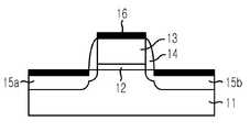
도 1은 종래 기술에 따른 MOS 트랜지스터를 도시한 단면도이다.1 is a cross-sectional view showing a MOS transistor according to the prior art.
도 1을 참조하면, 종래의 MOS 트랜지스터는 기판(11)에 형성된 웰(도시하지 않음)과 웰이 형성된 기판(11) 상에 형성되며 전도막(13)/산화막(12)의 적층 구조와 그 측벽의 스페이서(14)로 이루어진 게이트 전극과, 게이트 전극에 얼라인되어 기판(11)에 불순물 확산 방식으로 형성된 소스/드레인 접합(15a, 15b)을 구비하여 구성된다.Referring to FIG. 1, a conventional MOS transistor is formed on a well (not shown) formed on a
한편, 소스/드레인 접합(15a, 15b) 및 전도막(13) 상에는 저저항화를 위한 금속 실리사이드(16)가 형성되어 있다.On the other hand,
상기한 구조를 갖는 종래의 MOS 트랜지스터는 그 구조상 이온 주입 공정시의 문제점과 게이트 패터닝 시의 문제점 및 소스/드레인이 마주보는 구조로 인한 낮은 항복 전압의 문제점이 있다.
Conventional MOS transistors having the above-described structure have problems in ion implantation, gate patterning, and low breakdown voltage due to source / drain structures.
본 발명은 상기한 종래 기술의 문제점을 해결하기 위해 제안된 것으로, 공정 마진을 확보하면서 항복 전압 감소의 문제점을 개선할 수 있는 MOS 트랜지스터 및 그 제조 방법을 제공하는데 그 목적이 있다.
The present invention has been proposed to solve the above-described problems of the prior art, and an object thereof is to provide a MOS transistor and a method of manufacturing the same, which can improve the problem of reducing the breakdown voltage while securing a process margin.
상기 목적을 달성하기 위한 일 특징적인 본 발명의 MOS 트랜지스터 및 그 제조 방법은 게이트 형성 영역에 홈을 갖는 기판, 상기 홈의 내측을 따라 형성된 게이트 절연막, 상기 홈 내부에 형성된 게이트 전극, 상기 홈의 양측 기판에 형성된 소스/드레인 접합을 포함한다.One aspect of the present invention provides a MOS transistor and a method of manufacturing the same. Source / drain junctions formed in the substrate.
또한, 본 발명의 MOS 트랜지스터 및 그 제조 방법은 기판 내부에 웰을 형성하는 단계, 상기 웰이 형성된 기판에 소스/드레인 접합 형성을 위한 불순물 영역을 형성하는 단계, 상기 불순물 영역이 형성된 상기 기판을 선택적으로 식각하여 게이트 전극 영역을 정의하는 홈을 형성하는 단계, 상기 홈의 내측을 따라 게이트 절연막을 형성하는 단계, 및 상기 홈의 내부에서 상기 게이트 절연막 상에 게이트 전극을 형성하는 단계를 포함한다.
In addition, the MOS transistor of the present invention and a method of manufacturing the same may include forming a well inside a substrate, forming an impurity region for forming a source / drain junction on the substrate on which the well is formed, and selectively selecting the substrate on which the impurity region is formed. Etching to form a groove defining a gate electrode region, forming a gate insulating film along the inner side of the groove, and forming a gate electrode on the gate insulating film inside the groove.
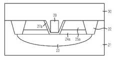
도 3은 본 발명의 실시예에 따른 MOS 트랜지스터의 구조를 나타내는 단면도로서, 게이트 형성 영역에 홈(36)을 갖는 기판(31)에, 홈(31)의 내측을 따라 게이트 절연막(37)을 형성하고, 홈(36) 내부에 형성된 게이트 전극(39)을 형성하고, 홈(36)의 양측 기판(31)에 형성된 소스/드레인 접합(38)을 포함한다.3 is a cross-sectional view illustrating a structure of a MOS transistor according to an exemplary embodiment of the present invention, in which a gate insulating film 37 is formed in a
이 때, 게이트 전극(39)에 전압이 인가되면, 게이트 전극(39) 하부의 웰(33)에 채널을 형성하여 트랜지스터가 동작하게 된다.
At this time, when a voltage is applied to the
이하, 본 발명이 속하는 기술 분야에서 통상의 지식을 가진 자가 본 발명의 기술적 사상을 용이하게 실시할 수 있을 정도로 상세히 설명하기 위하여, 본 발명의 가장 바람직한 실시예를 첨부 도면을 참조하여 설명하기로 한다.DETAILED DESCRIPTION OF THE PREFERRED EMBODIMENTS Hereinafter, preferred embodiments of the present invention will be described in detail with reference to the accompanying drawings in order to facilitate a person skilled in the art to easily carry out the technical idea of the present invention. .
도 3의 구조를 갖는 MOS 트랜지스터를 제조하기 위해 도 2a 내지 도 2i는 본 발명의 일실시예에 따른 NMOS 트랜지스터 제조 방법을 도시한 공정 단면도이다.2A to 2I are cross-sectional views illustrating a method of manufacturing an NMOS transistor according to an embodiment of the present invention to manufacture a MOS transistor having the structure of FIG. 3.
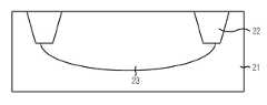
도 2a에 도시된 바와 같이, 반도체 기판(21)에 LOCOS(Local Oxidation of Silicon) 또는 STI(Shallow Trench Isolation) 방식을 이용하여 소자분리막(22)을 형성한다.As shown in FIG. 2A, the
도 2b에 도시된 바와 같이, 이온 주입 및 열확산 공정을 실시하여 소자분리막(22) 사이의 반도체 기판(21) 내부에 P웰(23)을 형성한다.As shown in FIG. 2B, the
P웰(23) 형성용 불순물로는 보론(B) 등을 사용하며, 불순물의 농도는 1.0×10¹² atoms/cm2~1.0×1014 atoms/cm2으로 한다.Boron (B) or the like is used as the impurity for forming the P well 23, and the impurity concentration is 1.0 × 10¹² atoms / cm2 to 1.0 × 10¹⁴ atoms / cm2 .
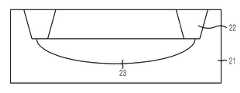
도 2c에 도시된 바와 같이, 선택적 이온 주입 및 열확산 공정을 실시하여 제 1불순물 영역(24)을 형성한다.As shown in FIG. 2C, a selective ion implantation and thermal diffusion process is performed to form the first impurity region 24.
이 때, 불순물은 인(P), 아세닌(As)이 사용되고, 불순물의 농도는 1.0×10¹² atoms/cm2~1.0×1013aatoms/cm2으로 주입한다.At this time, phosphorus (P) and acenin (As) are used as the impurity, and the impurity concentration is injected at 1.0 × 10¹² atoms / cm2 to 1.0 × 10¹³ a atoms / cm2 .
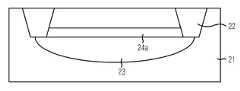
도 2d에 도시된 바와 같이, 선택적으로 이온 주입 및 열확산 공정을 실시하여 제 1불순물 영역(24) 상에 제 2불순물 영역(25)을 형성한다.As shown in FIG. 2D, an ion implantation and thermal diffusion process is optionally performed to form a second impurity region 25 on the first impurity region 24.
이 때, 불순물은 인(P), 아세닌(As)이 사용되고, 불순물의 농도는 1.0×10¹³ atoms/cm2~1.0×1016atoms/cm2으로 주입한다.At this time, phosphorus (P) and acenin (As) are used for the impurity, and the impurity concentration is injected at 1.0 × 10¹³ atoms / cm2 to 1.0 × 10¹⁶ atoms / cm2 .
제 1불순물 주입 공정과 제 2불순물 주입 공정은 소스/드레인을 형성하기 위한 공정이다.The first impurity implantation process and the second impurity implantation process are processes for forming a source / drain.
도 2e에 도시된 바와 같이, 웰(23), 제 1불순물 영역(24), 제 2불순물 영역 (25)이 적층된 구조 상에 트렌치 마스크(도시하지 않음)를 형성하고, 트렌치 마스크를 식각마스크로 사용하여 트렌치(26)를 형성한다.As shown in FIG. 2E, a trench mask (not shown) is formed on a structure in which the
도 2f에 도시된 바와 같이, 트렌치(26)가 형성된 반도체 기판(21)에 일정 두께로 게이트 절연막(27)을 형성한다. 이 때, 게이트 절연막(27)은 고온 열공정 또는 라디컬 산화와 같은 방법을 이용한다.As shown in FIG. 2F, the
도 2g에 도시된 바와 같이, 게이트 절연막(27)을 선택적으로 식각하여 트렌치(26) 내측면에만 0.03μm~0.1μm 두께의 게이트 절연막(27a)을 잔류하도록 한다. 이 때, 선택적 식각은 CMP 또는 전면 식각을 이용한다.As shown in FIG. 2G, the
한편, 반도체 기판(21) 내에서 게이트가 형성될 영역을 사이에 두고 서로 이격되어 소스/드레인(28) 영역이 형성된다. 소스/드레인(28) 영역은 저농도 소스/드레인 이온 주입, 고농도 소스/드레인 이온 주입을 차례로 실시한 것이다.Meanwhile, in the
도 2h에 도시된 바와 같이, 트렌치(24) 중심부에 게이트 전극(29)을 형성한다. 게이트 전극(29)을 선택적으로 식각하여 게이트 전극(29) 높이와 트렌치(24) 깊이가 같도록 한다. 게이트 전극(29)으로는 붕소가 도핑된 폴리실리콘, TiN과 같은 물질을 사용한다.As shown in FIG. 2H, the
이어서 도 2i에 도시된 바와 같이, 트렌치(26) 내부에 게이트 전극(29)이 형성된 결과물의 전면에 절연막(30)을 형성한다.Next, as illustrated in FIG. 2I, an insulating
절연막(30)으로는 BSG(Boro-Silicate-Glass)막, BPSG(Boro-Phospho-Silicate-Glass)막, PSG(Phospho-Silicate-Glass)막, TEOS(Tetra-Ethyl-Ortho-Silicate)막, HDP(High Density Plasma) 산화막, SOG(Spin On Glass)막 또는 APL(Advanced Planarization Layer)막 등을 이용하거나, 산화막 계열 이외에 무기 또는 유기 계열의 저유전율막을 이용한다.As the insulating
이어서, 게이트 전극(29)에 전압이 인가되면, 게이트 전극(29) 하부의 제 1불순물확산영역(23)에 채널을 형성하여 트랜지스터가 동작하게 된다.Subsequently, when a voltage is applied to the
상술한 바와 같이 이루어지는 본 발명은, 게이트 전극을 트렌치 내부에 매립하는 구조를 사용하여 LDD 영역을 생략하였므로, 게이트 전극 식각 공정시 발생하는 파티클에도 영향을 덜 받게 된다. 또한, 이온 주입 패턴의 경우, 크리티컬(critical) 부분에 대한 정의가 어려웠지만, 이온 주입 후 트렌치로 소스/드레인을 형성하여 디파인 문제를 해결하였음을 실시예를 통해 알아보았다.In the present invention as described above, since the LDD region is omitted by using a structure in which the gate electrode is embedded in the trench, particles generated during the gate electrode etching process are less affected. In addition, in the case of the ion implantation pattern, it was difficult to define the critical portion, but it was found through the example that the source / drain was formed by the trench after the ion implantation to solve the problem of fineness.
본 발명의 기술 사상은 상기 바람직한 실시예에 따라 구체적으로 기술되었으나, 상기한 실시예는 그 설명을 위한 것이며 그 제한을 위한 것이 아님을 주의하여야 한다. 또한, 본 발명의 기술 분야의 통상의 전문가라면 본 발명의 기술 사상의 범위 내에서 다양한 실시예가 가능함을 이해할 수 있을 것이다.
Although the technical idea of the present invention has been described in detail according to the above preferred embodiment, it should be noted that the above-described embodiment is for the purpose of description and not of limitation. In addition, it will be understood by those of ordinary skill in the art that various embodiments are possible within the scope of the technical idea of the present invention.
상술한 본 발명은 이온 주입 후 트렌치 내부에 게이트 전극을 구현함으로써 이온 주입 공정 패턴 단순화, LDD 공정 생략으로 공정을 단순화 할 수 있으며 게이트 산화막 식각시 게이트에 파티클 영향을 주지 않으므로 소자의 수율을 향상시킬 수 있다.The present invention described above can simplify the ion implantation process pattern by eliminating the LDD process by implementing the gate electrode inside the trench after the ion implantation, and improve the yield of the device because it does not affect the gate during the gate oxide etching. have.
또한, 소스/드레인이 마주보지 않고 아래를 향하기 때문에 항복 전압을 개선 하는 효과를 얻을 수 있다.
In addition, since the source / drain faces downward without facing, an effect of improving the breakdown voltage can be obtained.
Claims (14)
Translated fromKoreanPriority Applications (1)
| Application Number | Priority Date | Filing Date | Title |
|---|---|---|---|
| KR1020040115871AKR101128683B1 (en) | 2004-12-30 | 2004-12-30 | A mos transistor and method for fabricating the same |
Applications Claiming Priority (1)
| Application Number | Priority Date | Filing Date | Title |
|---|---|---|---|
| KR1020040115871AKR101128683B1 (en) | 2004-12-30 | 2004-12-30 | A mos transistor and method for fabricating the same |
Publications (2)
| Publication Number | Publication Date |
|---|---|
| KR20060077081A KR20060077081A (en) | 2006-07-05 |
| KR101128683B1true KR101128683B1 (en) | 2012-03-26 |
Family
ID=37169202
Family Applications (1)
| Application Number | Title | Priority Date | Filing Date |
|---|---|---|---|
| KR1020040115871AExpired - Fee RelatedKR101128683B1 (en) | 2004-12-30 | 2004-12-30 | A mos transistor and method for fabricating the same |
Country Status (1)
| Country | Link |
|---|---|
| KR (1) | KR101128683B1 (en) |
Citations (1)
| Publication number | Priority date | Publication date | Assignee | Title |
|---|---|---|---|---|
| KR20030022325A (en)* | 2001-05-30 | 2003-03-15 | 소니 가부시끼 가이샤 | Method for manufacturing channel gate type field effect transistor |
- 2004
- 2004-12-30KRKR1020040115871Apatent/KR101128683B1/ennot_activeExpired - Fee Related
Patent Citations (1)
| Publication number | Priority date | Publication date | Assignee | Title |
|---|---|---|---|---|
| KR20030022325A (en)* | 2001-05-30 | 2003-03-15 | 소니 가부시끼 가이샤 | Method for manufacturing channel gate type field effect transistor |
Also Published As
| Publication number | Publication date |
|---|---|
| KR20060077081A (en) | 2006-07-05 |
Similar Documents
| Publication | Publication Date | Title |
|---|---|---|
| KR100363353B1 (en) | Semiconductor device and manufacturing method thereof | |
| KR101201489B1 (en) | Method for fabricating soi device | |
| US7955919B2 (en) | Spacer-less transistor integration scheme for high-K gate dielectrics and small gate-to-gate spaces applicable to Si, SiGe and strained silicon schemes | |
| TWI548086B (en) | Ditch type lateral diffusion metal oxide semiconductor component and manufacturing method thereof | |
| US5777370A (en) | Trench isolation of field effect transistors | |
| KR100764918B1 (en) | Self-Aligned Source and Drain Extensions Made by Inlay Contact and Gate Processes | |
| US8053897B2 (en) | Production of a carrier wafer contact in trench insulated integrated SOI circuits having high-voltage components | |
| CN101447457B (en) | Method for manufacturing double-stress membrane complementary metal oxide semiconductor (CMOS) transistor | |
| US6365525B2 (en) | Method of fabricating a semiconductor insulation layer | |
| TW200908319A (en) | Junction field effect transistors in germanium and silicon-germanium alloys and method for making and using | |
| US6677194B2 (en) | Method of manufacturing a semiconductor integrated circuit device | |
| TWI525823B (en) | Integrated circuit device and method of manufacturing same | |
| US10243073B2 (en) | Vertical channel field-effect transistor (FET) process compatible long channel transistors | |
| CN101197369A (en) | Lateral MOS transistor and its manufacturing method | |
| US20090078998A1 (en) | Semiconductor device having decreased contact resistance | |
| KR100511590B1 (en) | Semiconductor device and method for fabrication thereof | |
| KR101128683B1 (en) | A mos transistor and method for fabricating the same | |
| US20120292688A1 (en) | Highly integrated mos device and the manufacturing method thereof | |
| KR101006519B1 (en) | Semiconductor device and manufacturing method thereof | |
| KR100386452B1 (en) | Method for manufacturing semiconductor device | |
| KR100689672B1 (en) | Manufacturing method of semiconductor device | |
| KR100880838B1 (en) | Method of manufacturing semiconductor device having recess gate | |
| KR100949665B1 (en) | Manufacturing method of semiconductor device | |
| KR100792404B1 (en) | Manufacturing Method of Semiconductor Device | |
| KR20060108304A (en) | Semiconductor device and manufacturing method |
Legal Events
| Date | Code | Title | Description |
|---|---|---|---|
| PA0109 | Patent application | St.27 status event code:A-0-1-A10-A12-nap-PA0109 | |
| PN2301 | Change of applicant | St.27 status event code:A-3-3-R10-R13-asn-PN2301 St.27 status event code:A-3-3-R10-R11-asn-PN2301 | |
| PG1501 | Laying open of application | St.27 status event code:A-1-1-Q10-Q12-nap-PG1501 | |
| A201 | Request for examination | ||
| PA0201 | Request for examination | St.27 status event code:A-1-2-D10-D11-exm-PA0201 | |
| R17-X000 | Change to representative recorded | St.27 status event code:A-3-3-R10-R17-oth-X000 | |
| E902 | Notification of reason for refusal | ||
| PE0902 | Notice of grounds for rejection | St.27 status event code:A-1-2-D10-D21-exm-PE0902 | |
| E13-X000 | Pre-grant limitation requested | St.27 status event code:A-2-3-E10-E13-lim-X000 | |
| P11-X000 | Amendment of application requested | St.27 status event code:A-2-2-P10-P11-nap-X000 | |
| P13-X000 | Application amended | St.27 status event code:A-2-2-P10-P13-nap-X000 | |
| E701 | Decision to grant or registration of patent right | ||
| PE0701 | Decision of registration | St.27 status event code:A-1-2-D10-D22-exm-PE0701 | |
| GRNT | Written decision to grant | ||
| PR0701 | Registration of establishment | St.27 status event code:A-2-4-F10-F11-exm-PR0701 | |
| PR1002 | Payment of registration fee | St.27 status event code:A-2-2-U10-U11-oth-PR1002 Fee payment year number:1 | |
| PG1601 | Publication of registration | St.27 status event code:A-4-4-Q10-Q13-nap-PG1601 | |
| FPAY | Annual fee payment | Payment date:20150223 Year of fee payment:4 | |
| PR1001 | Payment of annual fee | St.27 status event code:A-4-4-U10-U11-oth-PR1001 Fee payment year number:4 | |
| FPAY | Annual fee payment | Payment date:20160219 Year of fee payment:5 | |
| PR1001 | Payment of annual fee | St.27 status event code:A-4-4-U10-U11-oth-PR1001 Fee payment year number:5 | |
| FPAY | Annual fee payment | Payment date:20170216 Year of fee payment:6 | |
| PR1001 | Payment of annual fee | St.27 status event code:A-4-4-U10-U11-oth-PR1001 Fee payment year number:6 | |
| FPAY | Annual fee payment | Payment date:20180221 Year of fee payment:7 | |
| PR1001 | Payment of annual fee | St.27 status event code:A-4-4-U10-U11-oth-PR1001 Fee payment year number:7 | |
| P22-X000 | Classification modified | St.27 status event code:A-4-4-P10-P22-nap-X000 | |
| FPAY | Annual fee payment | Payment date:20190218 Year of fee payment:8 | |
| PR1001 | Payment of annual fee | St.27 status event code:A-4-4-U10-U11-oth-PR1001 Fee payment year number:8 | |
| FPAY | Annual fee payment | Payment date:20200218 Year of fee payment:9 | |
| PR1001 | Payment of annual fee | St.27 status event code:A-4-4-U10-U11-oth-PR1001 Fee payment year number:9 | |
| PN2301 | Change of applicant | St.27 status event code:A-5-5-R10-R11-asn-PN2301 | |
| PN2301 | Change of applicant | St.27 status event code:A-5-5-R10-R14-asn-PN2301 | |
| R18-X000 | Changes to party contact information recorded | St.27 status event code:A-5-5-R10-R18-oth-X000 | |
| PR1001 | Payment of annual fee | St.27 status event code:A-4-4-U10-U11-oth-PR1001 Fee payment year number:10 | |
| PC1903 | Unpaid annual fee | St.27 status event code:A-4-4-U10-U13-oth-PC1903 Not in force date:20220315 Payment event data comment text:Termination Category : DEFAULT_OF_REGISTRATION_FEE | |
| PN2301 | Change of applicant | St.27 status event code:A-5-5-R10-R13-asn-PN2301 St.27 status event code:A-5-5-R10-R11-asn-PN2301 | |
| PC1903 | Unpaid annual fee | St.27 status event code:N-4-6-H10-H13-oth-PC1903 Ip right cessation event data comment text:Termination Category : DEFAULT_OF_REGISTRATION_FEE Not in force date:20220315 | |
| P22-X000 | Classification modified | St.27 status event code:A-4-4-P10-P22-nap-X000 |