KR101128633B1 - Display device - Google Patents
Display deviceDownload PDFInfo
- Publication number
- KR101128633B1 KR101128633B1KR1020117005258AKR20117005258AKR101128633B1KR 101128633 B1KR101128633 B1KR 101128633B1KR 1020117005258 AKR1020117005258 AKR 1020117005258AKR 20117005258 AKR20117005258 AKR 20117005258AKR 101128633 B1KR101128633 B1KR 101128633B1
- Authority
- KR
- South Korea
- Prior art keywords
- fluid
- display device
- color
- layer
- support plate
- Prior art date
- Legal status (The legal status is an assumption and is not a legal conclusion. Google has not performed a legal analysis and makes no representation as to the accuracy of the status listed.)
- Expired - Lifetime
Links
- 239000012530fluidSubstances0.000claimsabstractdescription101
- 239000003086colorantSubstances0.000claimsdescription11
- 230000000694effectsEffects0.000claimsdescription7
- 230000002209hydrophobic effectEffects0.000claimsdescription6
- 238000006073displacement reactionMethods0.000abstractdescription2
- 239000003921oilSubstances0.000description60
- 239000010408filmSubstances0.000description23
- 230000005684electric fieldEffects0.000description14
- 239000000463materialSubstances0.000description9
- XLYOFNOQVPJJNP-UHFFFAOYSA-NwaterSubstancesOXLYOFNOQVPJJNP-UHFFFAOYSA-N0.000description9
- 239000012212insulatorSubstances0.000description5
- 239000006096absorbing agentSubstances0.000description4
- 239000000203mixtureSubstances0.000description4
- 230000003287optical effectEffects0.000description4
- 230000004888barrier functionEffects0.000description3
- 239000000975dyeSubstances0.000description3
- 239000011521glassSubstances0.000description3
- 239000000243solutionSubstances0.000description3
- 239000000758substrateSubstances0.000description3
- LFQSCWFLJHTTHZ-UHFFFAOYSA-NEthanolChemical compoundCCOLFQSCWFLJHTTHZ-UHFFFAOYSA-N0.000description2
- 238000005516engineering processMethods0.000description2
- DCAYPVUWAIABOU-UHFFFAOYSA-NhexadecaneChemical compoundCCCCCCCCCCCCCCCCDCAYPVUWAIABOU-UHFFFAOYSA-N0.000description2
- 239000002245particleSubstances0.000description2
- 239000004033plasticSubstances0.000description2
- 229920003023plasticPolymers0.000description2
- 229920003229poly(methyl methacrylate)Polymers0.000description2
- 239000004926polymethyl methacrylateSubstances0.000description2
- NIPNSKYNPDTRPC-UHFFFAOYSA-NN-[2-oxo-2-(2,4,6,7-tetrahydrotriazolo[4,5-c]pyridin-5-yl)ethyl]-2-[[3-(trifluoromethoxy)phenyl]methylamino]pyrimidine-5-carboxamideChemical compoundO=C(CNC(=O)C=1C=NC(=NC=1)NCC1=CC(=CC=C1)OC(F)(F)F)N1CC2=C(CC1)NN=N2NIPNSKYNPDTRPC-UHFFFAOYSA-N0.000description1
- 241000533901Narcissus papyraceusSpecies0.000description1
- 239000004809TeflonSubstances0.000description1
- 229920006362Teflon®Polymers0.000description1
- 229910010413TiO 2Inorganic materials0.000description1
- 230000002745absorbentEffects0.000description1
- 239000002250absorbentSubstances0.000description1
- 238000010521absorption reactionMethods0.000description1
- 150000001335aliphatic alkanesChemical class0.000description1
- 230000005540biological transmissionEffects0.000description1
- 230000015556catabolic processEffects0.000description1
- 230000021615conjugationEffects0.000description1
- 230000008878couplingEffects0.000description1
- 238000010168coupling processMethods0.000description1
- 238000005859coupling reactionMethods0.000description1
- 230000007423decreaseEffects0.000description1
- 238000006731degradation reactionMethods0.000description1
- 238000009792diffusion processMethods0.000description1
- 235000019441ethanolNutrition0.000description1
- 239000004811fluoropolymerSubstances0.000description1
- 229920002313fluoropolymerPolymers0.000description1
- -1hexadecaneChemical class0.000description1
- AMGQUBHHOARCQH-UHFFFAOYSA-Nindium;oxotinChemical compound[In].[Sn]=OAMGQUBHHOARCQH-UHFFFAOYSA-N0.000description1
- 239000007788liquidSubstances0.000description1
- 238000004519manufacturing processMethods0.000description1
- 230000005693optoelectronicsEffects0.000description1
- 230000000149penetrating effectEffects0.000description1
- 239000000049pigmentSubstances0.000description1
- 229920000052poly(p-xylylene)Polymers0.000description1
- 229920000642polymerPolymers0.000description1
- 230000001681protective effectEffects0.000description1
- 230000002441reversible effectEffects0.000description1
- 239000012266salt solutionSubstances0.000description1
- 230000035945sensitivityEffects0.000description1
- 229920002545silicone oilPolymers0.000description1
- 239000007787solidSubstances0.000description1
- 239000010409thin filmSubstances0.000description1
Images


Classifications
- G—PHYSICS
- G02—OPTICS
- G02F—OPTICAL DEVICES OR ARRANGEMENTS FOR THE CONTROL OF LIGHT BY MODIFICATION OF THE OPTICAL PROPERTIES OF THE MEDIA OF THE ELEMENTS INVOLVED THEREIN; NON-LINEAR OPTICS; FREQUENCY-CHANGING OF LIGHT; OPTICAL LOGIC ELEMENTS; OPTICAL ANALOGUE/DIGITAL CONVERTERS
- G02F1/00—Devices or arrangements for the control of the intensity, colour, phase, polarisation or direction of light arriving from an independent light source, e.g. switching, gating or modulating; Non-linear optics
- G02F1/01—Devices or arrangements for the control of the intensity, colour, phase, polarisation or direction of light arriving from an independent light source, e.g. switching, gating or modulating; Non-linear optics for the control of the intensity, phase, polarisation or colour
- G02F1/165—Devices or arrangements for the control of the intensity, colour, phase, polarisation or direction of light arriving from an independent light source, e.g. switching, gating or modulating; Non-linear optics for the control of the intensity, phase, polarisation or colour based on translational movement of particles in a fluid under the influence of an applied field
- G02F1/166—Devices or arrangements for the control of the intensity, colour, phase, polarisation or direction of light arriving from an independent light source, e.g. switching, gating or modulating; Non-linear optics for the control of the intensity, phase, polarisation or colour based on translational movement of particles in a fluid under the influence of an applied field characterised by the electro-optical or magneto-optical effect
- G02F1/167—Devices or arrangements for the control of the intensity, colour, phase, polarisation or direction of light arriving from an independent light source, e.g. switching, gating or modulating; Non-linear optics for the control of the intensity, phase, polarisation or colour based on translational movement of particles in a fluid under the influence of an applied field characterised by the electro-optical or magneto-optical effect by electrophoresis
- G—PHYSICS
- G02—OPTICS
- G02B—OPTICAL ELEMENTS, SYSTEMS OR APPARATUS
- G02B26/00—Optical devices or arrangements for the control of light using movable or deformable optical elements
- G02B26/004—Optical devices or arrangements for the control of light using movable or deformable optical elements based on a displacement or a deformation of a fluid
- G02B26/005—Optical devices or arrangements for the control of light using movable or deformable optical elements based on a displacement or a deformation of a fluid based on electrowetting
- G—PHYSICS
- G02—OPTICS
- G02F—OPTICAL DEVICES OR ARRANGEMENTS FOR THE CONTROL OF LIGHT BY MODIFICATION OF THE OPTICAL PROPERTIES OF THE MEDIA OF THE ELEMENTS INVOLVED THEREIN; NON-LINEAR OPTICS; FREQUENCY-CHANGING OF LIGHT; OPTICAL LOGIC ELEMENTS; OPTICAL ANALOGUE/DIGITAL CONVERTERS
- G02F1/00—Devices or arrangements for the control of the intensity, colour, phase, polarisation or direction of light arriving from an independent light source, e.g. switching, gating or modulating; Non-linear optics
- G02F1/01—Devices or arrangements for the control of the intensity, colour, phase, polarisation or direction of light arriving from an independent light source, e.g. switching, gating or modulating; Non-linear optics for the control of the intensity, phase, polarisation or colour
- G02F1/17—Devices or arrangements for the control of the intensity, colour, phase, polarisation or direction of light arriving from an independent light source, e.g. switching, gating or modulating; Non-linear optics for the control of the intensity, phase, polarisation or colour based on variable-absorption elements not provided for in groups G02F1/015 - G02F1/169
- G—PHYSICS
- G09—EDUCATION; CRYPTOGRAPHY; DISPLAY; ADVERTISING; SEALS
- G09F—DISPLAYING; ADVERTISING; SIGNS; LABELS OR NAME-PLATES; SEALS
- G09F9/00—Indicating arrangements for variable information in which the information is built-up on a support by selection or combination of individual elements
- G09F9/30—Indicating arrangements for variable information in which the information is built-up on a support by selection or combination of individual elements in which the desired character or characters are formed by combining individual elements
- G09F9/37—Indicating arrangements for variable information in which the information is built-up on a support by selection or combination of individual elements in which the desired character or characters are formed by combining individual elements being movable elements
- G09F9/372—Indicating arrangements for variable information in which the information is built-up on a support by selection or combination of individual elements in which the desired character or characters are formed by combining individual elements being movable elements the positions of the elements being controlled by the application of an electric field
- G—PHYSICS
- G02—OPTICS
- G02B—OPTICAL ELEMENTS, SYSTEMS OR APPARATUS
- G02B2207/00—Coding scheme for general features or characteristics of optical elements and systems of subclass G02B, but not including elements and systems which would be classified in G02B6/00 and subgroups
- G02B2207/115—Electrowetting
- G—PHYSICS
- G02—OPTICS
- G02F—OPTICAL DEVICES OR ARRANGEMENTS FOR THE CONTROL OF LIGHT BY MODIFICATION OF THE OPTICAL PROPERTIES OF THE MEDIA OF THE ELEMENTS INVOLVED THEREIN; NON-LINEAR OPTICS; FREQUENCY-CHANGING OF LIGHT; OPTICAL LOGIC ELEMENTS; OPTICAL ANALOGUE/DIGITAL CONVERTERS
- G02F1/00—Devices or arrangements for the control of the intensity, colour, phase, polarisation or direction of light arriving from an independent light source, e.g. switching, gating or modulating; Non-linear optics
- G02F1/01—Devices or arrangements for the control of the intensity, colour, phase, polarisation or direction of light arriving from an independent light source, e.g. switching, gating or modulating; Non-linear optics for the control of the intensity, phase, polarisation or colour
- G02F1/165—Devices or arrangements for the control of the intensity, colour, phase, polarisation or direction of light arriving from an independent light source, e.g. switching, gating or modulating; Non-linear optics for the control of the intensity, phase, polarisation or colour based on translational movement of particles in a fluid under the influence of an applied field
- G02F1/1675—Constructional details
- G02F2001/1678—Constructional details characterised by the composition or particle type
Landscapes
- Physics & Mathematics (AREA)
- General Physics & Mathematics (AREA)
- Optics & Photonics (AREA)
- Nonlinear Science (AREA)
- Engineering & Computer Science (AREA)
- Theoretical Computer Science (AREA)
- Chemical & Material Sciences (AREA)
- Life Sciences & Earth Sciences (AREA)
- Health & Medical Sciences (AREA)
- Chemical Kinetics & Catalysis (AREA)
- Electrochemistry (AREA)
- Molecular Biology (AREA)
- Electrochromic Elements, Electrophoresis, Or Variable Reflection Or Absorption Elements (AREA)
- Devices For Indicating Variable Information By Combining Individual Elements (AREA)
- Vehicle Body Suspensions (AREA)
- Diaphragms For Electromechanical Transducers (AREA)
- Measuring Pulse, Heart Rate, Blood Pressure Or Blood Flow (AREA)
Abstract
Translated fromKoreanDescription
Translated fromKorean본 발명은 제 1 지지판과 제 2 지지판 사이의 공간 내에 서로 혼합되지 않는 적어도 하나의 제 1 유체와 제 2 유체를 가지는 화상 요소를 포함하는 디스플레이 디바이스로서, 상기 유체 중 하나는 전도성 즉 극성이며, 상기 디바이스는 적어도 2개의 다른 상태를 생성하기 위한 수단을 포함하는, 디스플레이 디바이스에 관한 것이다.A display device comprising an image element having at least one first fluid and a second fluid that do not mix with each other in a space between a first support plate and a second support plate, wherein one of the fluids is conductive or polarized, and The device relates to a display device, comprising means for generating at least two different states.
본 발명은 스위칭 가능한 확산 디바이스에 더 관한 것이다.The invention further relates to a switchable diffusion device.
TFT-LCD와 같은 디스플레이 디바이스는 랩탑 컴퓨터(laptop computer)에서 그리고 오거나이저(organizer)에서 사용되고 있지만 또한 GSM 전화에도 점차 더 널리 응용되고 있다. LCD 대신에, 예를 들어 (폴리머) LED 디스플레이 디바이스 또한 사용되고 있다.Display devices, such as TFT-LCDs, are used in laptop computers and in organizers, but also increasingly in GSM phones. Instead of LCDs, for example (polymer) LED display devices are also used.
지금까지 잘 확립된 이들 디스플레이 효과와는 별도로 페이퍼 화이트 응용(paper white applications)에 적합한 전기영동 디스플레이(electrophoretic displays)와 같이 다른 디스플레이 기술이 개발되고 있다.Apart from these well established display effects to date, other display technologies are being developed, such as electrophoretic displays suitable for paper white applications.
확산 디바이스(diffusing device)는 카메라와 같은 몇몇 디바이스에 사용될 수 있다.Diffusing devices can be used in some devices, such as cameras.
본 발명에 따른 디스플레이 디바이스는 적어도 2개의 다른 상태를 구비하며, 여기서 유체 중 하나는 제 1 상태에서 적어도 제 1 지지판에 인접하며 제 2 상태에서 다른 유체는 이 제 1 지지판에 적어도 부분적으로 인접하여 있다.The display device according to the invention has at least two different states, in which one of the fluids is adjacent to at least the first support plate in the first state and the other fluid is at least partially adjacent to the first support plate in the second state. .
본 발명은 소위 층의 브레이크업(breakup) 그러나 다른 한편 층의 이동(displacement)이 사용될 수 있는 본 발명자에 의해 발견된 원리에 기초를 두고 있다. 본 발명은 이들 원리를 사용하는 새로운 방식을 제공한다.The present invention is based on the principle found by the inventors so-called breakup of layers but on the other hand displacement of layers can be used. The present invention provides a new way of using these principles.
예를 들어, (제 1) 유체가 (컬러) 오일이고 제 2 (다른) 유체가 (계면 장력으로 인해) 물이라면, 오일 층의 위에 물 층을 포함하는 두 개의 층 시스템이 제공된다. 그러나, 두 개의 층 사이에 전압이 인가되는 경우, 오일 층은 정전력 (electrostatic forces)으로 인해 브레이크업(break up)된다. 물 부분이 이제 오일 층을 뚫고 들어가기 때문에 화상 요소는 부분적으로 투명하게 된다.For example, if the (first) fluid is (color) oil and the second (other) fluid is water (due to interface tension), a two layer system is provided that includes a water layer on top of the oil layer. However, when a voltage is applied between the two layers, the oil layer breaks up due to electrostatic forces. The image element is partially transparent because the water portion now penetrates the oil layer.
브레이크업 후에 남아 있는 (제 1) 유체 ((컬러) 오일)의 액적(droplet)에 의해 점유되는 면적 비율(fraction of area)만큼 그 콘트라스트는 제한된다. 일반적으로, 원래 유체 층의 두께에 따라 25-50%의 면적이 실현된다. 이것은 더 높은 전압을 인가함으로써 더 감소될 수 있으나, 이는 소비 전력을 크게 증가시킬 수 있다. 이상적으로, 유체, 이 경우에는 광학적으로 흡수 오일(optically absorbing oil)에 의해 점유되는 나머지 면적을 0%로 접근하게 하는 것이 좋을 것이다.The contrast is limited by the fraction of area occupied by droplets of (first) fluid ((color) oil) remaining after breakup. In general, an area of 25-50% is realized depending on the thickness of the original fluid layer. This can be further reduced by applying a higher voltage, but this can greatly increase the power consumption. Ideally, it would be nice to have the remaining area occupied by the fluid, in this case optically absorbing oil, approach 0%.
브레이크업 시에 그 면적 비율이 순간적으로 약 50%로 줄어드는 다른 제한이 있다. 그리하여 100%에 가까운 면적 비율을 얻는 것이 곤란하다. 그 결과 아날로그 그레이 스케일을 실현하는 것이 곤란하게 될 수 있다.There is another limitation when the area of the breakup is reduced to about 50% instantaneously. Thus, it is difficult to obtain an area ratio close to 100%. As a result, it may be difficult to realize the analog gray scale.
본 발명에 따른 디스플레이 디바이스는, 소수성 층(hydrophobic layer)을 구비하는 제 1 지지판과 제 2 지지판 사이의 공간 내에 서로 혼합되지 않는 적어도 하나의 제 1 유체와, 전기전도성 또는 극성인 제 2 유체를 구비하는 화상 요소를 포함하며, 상기 디바이스의 화상 요소는 인가된 전계가 없는 적어도 제 1 상태와, 인가된 전계가 있는 제 2 상태 사이에서 전기적으로 전환될 수(switchable) 있고, 상기 제 1 상태에서 상기 제 1 유체는 상기 화상 요소 내에서 확산되어 상기 제 1 지지판의 영역에 인접하고, 상기 제 2 상태에서 상기 제 2 유체는 상기 제 1 지지판의 상기 영역에 인접하고, 상기 제 1 유체는 상기 화상 요소의 측면으로 수축되며, 상기 상태들은 상기 영역 위에서 디스플레이 효과를 제공하고, 상기 영역은 상기 소수성 층의 영역이고, 상기 제 1 유체는 상기 제 1 상태와 상기 제 2 상태에서 상기 화상 요소의 공간에 한정된 구성을 갖는다.A display device according to the invention comprises at least one first fluid which does not mix with each other in a space between a first support plate and a second support plate having a hydrophobic layer and a second fluid which is electrically conductive or polarized. A picture element of the device, wherein the picture element of the device is electrically switchable between at least a first state with no applied electric field and a second state with an applied electric field, A first fluid diffuses in the image element and is adjacent to the area of the first support plate, and in the second state the second fluid is adjacent to the area of the first support plate and the first fluid is the image element. Contracted to the side of the states, the states provide a display effect above the region, the region being the region of the hydrophobic layer, and the first fluid It has a configuration limited to the space of the image element in the first state and the second state.
제 1 실시예에서, 화상 요소는 한정된 공간(예를 들어, 거의 밀폐된 공간)에 대응하며 제 2 상태에서 다른 유체는 제 1 지지판에 거의 완전히 인접하여 있다. 본 발명의 다른 측면에 따라 이것은 균일하지 않은 전계(inhomogeneous electric field)를 적용하는 것에 의해 달성된다. 이 경우에, 층의 브레이크업(또는 이동)을 위한 임계 전계(threshold field)는 어떤 특정 위치에서만 초과할 수 있다. 이들 위치에서 오일 필름의 브레이크업(또는 이동)이 개시될 수 있다. 균일하지 않게 인가되는 전계는 여러 가지 방식으로 얻어질 수 있다.In the first embodiment, the image element corresponds to a confined space (e.g. an almost closed space) and in the second state the other fluid is almost completely adjacent to the first support plate. According to another aspect of the invention this is achieved by applying an inhomogeneous electric field. In this case, the threshold field for breakup (or movement) of the floor may exceed only at certain locations. At these positions breakup (or movement) of the oil film can be initiated. An unevenly applied electric field can be obtained in many ways.
이 목적을 위해 본 발명의 선호되는 제 1 실시예에서 제 1 지지판의 일부면과 전극 사이에 있는 유전 층이 두께에 있어 변화한다.For this purpose, in the first preferred embodiment of the invention, the dielectric layer between some surface of the first support plate and the electrode varies in thickness.
다른 실시예에서, 제 1 지지판의 일부면과 전극 사이의 유전 층이 가변적인 유전 상수(dielectric constant)를 가진다.In another embodiment, the dielectric layer between some face of the first support plate and the electrode has a variable dielectric constant.
전계를 증가시키는 것에 의해 오일 필름의 브레이크업(또는 이동)을 위한 임계값이 지지판의 면적에 대해 이동되고 제어될 수 있다. 이것은 그레이 레벨(grey level)의 실현을 가능하게 한다.By increasing the electric field, the threshold for breakup (or movement) of the oil film can be moved and controlled relative to the area of the support plate. This makes it possible to realize gray levels.
다른 한편으로, 오일 필름의 브레이크업(또는 이동)은 제 1 지지판의 일부의 습윤율(wettability) 또는 제 1 유체 층의 두께를 변화시켜서 제어될 수 있다.On the other hand, breakup (or movement) of the oil film can be controlled by varying the wettability of the portion of the first support plate or the thickness of the first fluid layer.
나아가, 전극 에지(edge)에 스트레이 전계 분포(stray field distribution)를 사용하는 것이나 또는 원하는 균일하지 않은 전계 분포를 제공하는 분할된 전극 구조를 심지어 디자인 하는 것도 가능하다.Furthermore, it is possible to use a stray field distribution at the electrode edges or even to design a split electrode structure that provides the desired non-uniform field distribution.
본 발명에 따른 다른 실시예에서, 화상 요소는 한정된 공간에 대응하며 제 1 상태에서 다른 유체 층은 두 지지판에 거의 완전히 인접하여 있다. 사실, 다른 유체 층(오일 층)은 이제 2개의 하위 층으로 분할되며 이 하위 층은 각각 더 얇을 수 있다. 이것은 한편으로 더 낮은 전압을 사용하여 오일 필름 브레이크업(또는 이동)이 일어나게 할 수 있다. 다른 한편으로, 이것은 디스플레이를 착색할 기회를 제공하며 더 많은 다채로운 그레이 값(gray value)의 실현을 가능하게 한다.In another embodiment according to the invention, the image element corresponds to a confined space and in the first state the other fluid layer is almost completely adjacent to the two support plates. In fact, the other fluid layer (oil layer) is now divided into two sublayers, each of which may be thinner. This, on the one hand, can cause oil film breakup (or movement) to occur using lower voltages. On the other hand, this offers the opportunity to color the display and enables the realization of more colorful gray values.
이 목적을 위해 본 발명의 선호되는 실시예에서 화상 요소는 상기 공간을 적어도 2개의 서브 화상 요소로 분할하는 추가적인 벽부를 갖는 한정된 공간에 대응하며 여기서 제 1 상태에서 추가적인 다른 유체 층은 서브 화상 요소 내에 적어도 부분적으로 상기 제 1 지지판에 인접하여 있다. 상기 (추가적인) 다른 유체 층에 다른 컬러를 제공하는 것에 의해 컬러 디스플레이가 얻어진다.For this purpose in a preferred embodiment of the present invention the picture element corresponds to a confined space with an additional wall which divides the space into at least two sub picture elements, wherein in the first state an additional further fluid layer is present in the sub picture element. At least partially adjacent the first support plate. By providing different colors to the (additional) other fluid layers, a color display is obtained.
브레이크업 후에 추가적인 유체에 의해 점유되는 나머지 영역을 얻기 위해 제 2 상태에서 다른 유체 층과 추가적인 다른 유체 층의 적어도 하나는 상기 공간의 벽부에 인접하여 있다. 상기 벽부에 인접한 두 하위 층의 물질이 서로 혼합되는 것을 막기 위해, 상기 디바이스는 다른 유체 층의 일부와 추가적인 다른 유체 층이 제 2 상태에서 상호 혼합되는 것을 방지하기 위한 수단을 바람직하게는 포함한다.At least one of the other fluid layer and the other additional fluid layer in the second state is adjacent to the wall portion of the space in order to obtain the remaining area occupied by the additional fluid after break up. In order to prevent the materials of the two lower layers adjacent to the wall from mixing with each other, the device preferably comprises means for preventing some of the other fluid layer and the further other fluid layer from intermixing in the second state.
본 발명의 이들 측면과 다른 측면은 이하 기술되는 실시예를 참조하여 명백하며 명료하게 기술될 것이다.These and other aspects of the invention will be apparent from and elucidated with reference to the embodiments described below.
도 1 은 본 발명에 따른 디스플레이 디바이스의 일부 단면을 개략적으로 도시하는 도면.
도 2 는 본 발명에 따른 디스플레이 디바이스의 다른 일부 단면을 개략적으로 도시하는 도면.
도 3 은 본 발명에 따른 디스플레이 디바이스의 일부 개략도.
도 4 는 본 발명에 따른 컬러 디스플레이 디바이스의 일부 단면을 도시하는 도면.
도 5, 도 6, 및 도 7 은 본 발명의 추가 실시예를 도시하는 도면.
도 8 은 본 발명에 따른 디스플레이 디바이스의 다른 일부 단면을 개략적으로 도시하는 도면.1 shows schematically a partial cross section of a display device according to the invention;
2 schematically shows another partial cross section of a display device according to the invention;
3 is a partial schematic view of a display device according to the invention.
4 shows a partial cross section of a color display device according to the invention;
5, 6, and 7 illustrate further embodiments of the present invention.
8 schematically shows another partial cross section of a display device according to the invention;
본 도면들은 개략적인 것이며 축척에 맞지 않다. 대응하는 요소는 전체적으로 동일한 참조 부호에 의해 표시되어 있다.The figures are schematic and are not to scale. Corresponding elements are denoted by the same reference numerals throughout.
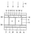
도 1 은 본 발명에 따른 디스플레이 디바이스(1)의 일부 단면을 개략적으로 도시한다. 2개의 투명 기판, 즉 제 1 지지판(3,7,8)과 제 2 지지판(4) 사이에는 서로 혼합되지 않는 제 1 유체(5)와 제 2 유체(6)가 제공된다. 제 1 유체(5)는 예를 들어 헥사데칸 (hexadecane)과 같은 알칸(alkane)이거나 또는 이 예에서와 같이 (실러콘 (silicone) 오일(oil)이다. 제 2 유체(6)는 전도성 즉 극성이며 예를 들어 물 또는 식염 용액(salt solution)(예를 들어, 물과 에틸 알코올을 혼합한 KCL 용액)이다. 제 1 상태에서, 외부 전압이 가해지지 않을 때(도 1a), 유체(5, 6)는 예를 들어 유리 또는 플라스틱 판(3,4)을 포함하는 제 1 지지판(3,7,8)과 제 2 투명 지지판(4)에 인접하여 있다. 유리 또는 플라스틱 판(3) 상에는 투명 전극(7), 예를 들어, 인듐(주석) 산화물이 제공되며 중간 소수성 층(intermediate hydrophobic layer)(8), 이 예에서 비정질 플루오로폴리머 (AF1600)가 제공된다.1 schematically shows a partial cross section of a
본 발명자는 전압이 가해질 때 (전압원(9)) 층(5)이 작은 액적으로 브레이크업(도 1b에서 단편화된 필름)되는 것을 발견하였다. 이 브레이크업(breakup)은, 전기에너지 이득이 곡선면의 생성으로 인해 표면 에너지 손실보다 더 큰 경우 일어난다. 매우 중요한 측면으로서, 연속 필름과 단편화된 필름 사이의 가역적인 스위칭이 전기 스위칭 수단(전압원(9))에 의하여 달성되는 것이 발견되었다.The inventors have found that when voltage is applied (voltage source 9)
이 효과는, 전기광학효과(electro-optical effect), 특히 컬러 오일이 사용되는 경우, 디스플레이 효과에 사용될 수 있다. 이것은 광학적으로 활성 오일 (optically active oil), 예를 들어, 불투명하거나 반사성의 오일에 의해 달성된다. 다른 실시예에서, 광학적으로 활성 입자를 갖는 유체가 사용되거나 또는 염료 물질(dye material)이 오일에 용해된다. 전기 광학 효과는 예를 들어 LCD 기술로부터 알려진 바와 같은 백라이트(back light)를 사용하는 것에 의해 투명 방식으로 또는, 반사체(reflector) 또는 확산 반사체(diffusive reflector)를 사용하는 것에 의해 반사 방식으로 사용될 수 있다.This effect can be used for the electro-optical effect, especially for display effects when color oils are used. This is achieved by optically active oils, for example opaque or reflective oils. In another embodiment, a fluid with optically active particles is used or a dye material is dissolved in oil. The electro-optic effect can be used in a transparent manner, for example by using a back light as known from LCD technology, or in a reflective manner by using a reflector or a diffuse reflector. .
액적의 사이즈는 가해지는 전압에 따라 달라지며, 이는 원리적으로 중간 투과(또는 반사) 상태(그레이 레벨)를 생성할 수 있는 가능성을 제공한다. 그러나, 브레이크업 시에 면적 비율(area fraction)이 실제 순간적으로 약 50%로 줄어든다는 것이 또한 발견되었다. 그리하여 50% 및 100% 사이의 면적 비율을 얻는 것이 곤란하다. 그 결과, 이 특정 범위 내에 임의의 아날로그 그레이 스케일이 실현되는 것이 곤란하게 된다.The size of the droplets depends on the voltage applied, which in principle offers the possibility of creating an intermediate transmission (or reflection) state (gray level). However, it has also been found that in breakup the area fraction is actually reduced to about 50% in real time. Thus, it is difficult to obtain an area ratio between 50% and 100%. As a result, it becomes difficult to realize any analog gray scale within this specific range.
다른 한편, 브레이크업 후에 생기는 액적에 의해 점유되는 면적 비율에 의해 그 콘트라스트가 제한된다. (IC 드라이버에 의해 디스플레이를 구동하는 것을 고려하여) 실제 전압에서는 약 25%의 최소 면적 비율이 관찰되는 것을 본다. 이것은 더 높은 전압을 인가함으로써 더 줄어들 수 있으나, 이는 소비 전력을 크게 증가시킬 수 있고 또한 저 전압 IC 드라이버의 사용을 못하게 할 수도 있다.On the other hand, the contrast is limited by the area ratio occupied by the droplets generated after the breakup. We see that a minimum area ratio of about 25% is observed at the actual voltage (considering driving the display by the IC driver). This can be further reduced by applying a higher voltage, but this can greatly increase power consumption and also prevent the use of low voltage IC drivers.
이를 위해, 도 2의 실시예에서, 중간 소수성 층(8)이 중앙에 최소의 두께를 갖는 곡선 형태를 취하며, 이는 화상 요소(2)의 중앙에서 전계가 최대로 되는 것을 보장해 준다. 이 경우에, 반경 방향으로 (절연체(insulator))의 두께를 변경시키는 것에 의해) 그 전계가 변화된다. 임계 전계는, 절연체가 최소의 두께를 갖는 픽셀의 중앙에서 먼저 초과된다. 전계를 증가시킬 때, 가해지는 전계가 임계 전계와 같아지는 위치가 외부 방향(outward)으로 이동하여, 그리하여 오일을 픽셀의 측면으로 이동시킨다. 도 3의 개략도는 원 대칭이거나 또는 직사각형 형상 중 어느 하나를 갖는 픽셀의 단면을 보여준다. 이 경우에, 오일은 픽셀의 중앙에 있는 단일 지점으로부터 시작하여 링형 형상(ring-like shape)으로 외부 방향(outward)으로 밀릴 수 있다. 직사각형 픽셀에서, 우리는 오일 브레이크업이 라인을 따라 시작할 수 있도록 그리고 오일은 커튼 방식(curtain-like fashion)으로 외부로 밀리도록 실린더 슬라이스(slice of cylinder)와 같은 형상의 절연체를 생각할 수 있다.To this end, in the embodiment of FIG. 2, the intermediate
층(8)의 이 곡선 형태를 도입함으로써, 광학적으로 흡수성 오일 층(5)은 광학적 활성이 더 이상 관련성이 없는 픽셀 내부 위치로 이동되며, 이 경우에는 픽셀의 측면(또는 뒷면)으로 이동된다. 특정 임계 전계(Et) 미만에서는, 브레이크업이 일어나지 않는 반면, Et보다 더 높은 전계에서는 오일 필름이 액적으로 브레이크업된다. 브레이크업은 절연체 두께(0.3-10㎛)의 광범위한 범위에 걸쳐 약 3V/㎛의 전계 강도에서 일어나는 것으로 관측되었다.By introducing this curved form of the
다른 예에서, 전극의 에지(edge)에 스트레이 전계 분포(stray field distribution)가 사용되거나 또는 원하는 균일하지 않은 전계 분포를 제공하는 특수 전극 구조(분할된 구조, 관통 구조)가 사용된다.In another example, a stray field distribution is used at the edge of the electrode, or a special electrode structure (divided structure, penetrating structure) is used that provides the desired non-uniform field distribution.
이 예에서, 오일 브레이크업이 고려되었지만, 유사한 논의가 유체의 이동에 기초하는 디바이스에도 적용된다. 다른 한편, (예를 들어, 불충분한 부피, 두께 변동 또는 접촉각으로 인해) 균일하지 않은 오일 층이 오일의 이동(또는 브레이크업)을 일으킬 수 있다.In this example, oil breakup was considered, but a similar discussion applies to devices based on the movement of the fluid. On the other hand, an uneven oil layer (e.g. due to insufficient volume, thickness variation or contact angle) can cause the oil to move (or break up).
두꺼운 오일 필름(5)에 대해 오일 필름이 브레이크업 되는 경우에 오일 필름의 두께는 더 이상 절연체(8)의 두께에 비해 무시할 수 없으며 더 높은 전압이 오일 필름의 브레이크업을 얻기 위해 필요하다. 그러므로, 이 원리는 (약 300㎚에 이르기까지는) 얇은 필름의 사용으로 제한된다. 그러한 두께의 필름에 대해 충분한 광 흡수율(optical absorption)을 가지는 것이 곤란하며, 이는 온 상태와 오프 상태 사이에 줄어든 광학적 콘트라스트를 생산한다.In the case where the oil film breaks up against the
이동의 경우에 픽셀에 걸쳐 변화하는 표면 장력을 효과적으로 야기하는 균일하지 않은 전계 분포가 사용된다. 이제, 총 시스템은 최저 표면 에너지를 갖는 위치(들)로 오일을 이동시키는 것에 의해 그 에너지를 낮출 수 있으며 우리는 오일 필름을 보이지 않게 이동시킬 수 있다. 이 원리는 얇은 오일 필름 뿐만 아니라 더 두꺼운 오일 필름에 대해서도 비교적 저 전압에서 작동하며 이는 오일 필름의 광학적 흡수성(optical absorptivity)에 대한 요구조건을 완화시킨다. 나아가, 이 원리는 그레이 값을 실현할 수 있게 한다.In the case of movement a non-uniform electric field distribution is used which effectively results in varying surface tensions across the pixels. Now, the total system can lower that energy by moving the oil to the location (s) with the lowest surface energy and we can move the oil film invisibly. This principle operates at relatively low voltages for thicker oil films as well as thinner oil films, which relaxes the requirement for optical absorptivity of the oil film. Furthermore, this principle makes it possible to realize gray values.
다른 실시예가 도 4에 도시되며, 도 4 는 유체(물)(6)의 양 측면에 2개의 별도의 오일 층(5, 5')을 포함한다.Another embodiment is shown in FIG. 4, which comprises two
층(8, 8')의 물질(예를 들어, AF 1600과 같은 테프론)과는 다른 물질 중에서 픽셀 벽부(13)를 제조하거나 또는
위에 제공된 부등성이 적용되는 물질의 일부 예는 파릴렌(parylene), PMMA(폴리메틸메타크릴레이트) 및 유리이다.Some examples of materials to which the inequality provided above are applied are parylene, PMMA (polymethylmethacrylate) and glass.
층(5, 5')에 다른 컬러를 제공하는 것에 의해 예를 들어 염료를 도입하는 것에 의해 컬러 디스플레이가 실현된다. 이것은 그 다음 예에서 설명된다.By providing different colors to the
예 1-3 컬러 디스플레이Example1-3 color display
도 5의 실시예에서, 오일(5)은 컬러 디스플레이를 실현하기 위해 다른 염료를 사용하는 것에 의해 다른 컬러를 가진다. 이 예에서, 예를 들어 3종류의 오일이 사용되는데, 다시 말해, 적색 층(5R), 녹색 층(5G) 및 청색 층(5B)이 도 5에 도시된 구성을 위해 최대 가능한 브라이트니스(brightness)를 얻기 위해 사용된다. 단일 픽셀은 흑색 흡수체(black absorber)(23)(백그라운드)와 2개의 서브 픽셀(A 및 B)을 포함하며, 각 서브픽셀은 도 4에 도시된 것과 유사한 구성을 갖는다. 제 1 상태에서 상부에 있는 오일 층(5B)은 서브 픽셀 각각의 절반을 커버한다. 이것은 층(8')(AF1600)의 표면 에너지를 국부적으로 변경하는 것에 의해 달성될 수 있다. 다른 유체, 이 경우에 물은 전극(12)을 통해 고정 전압, 예를 들어 접지(0V)에 있다고 가정한다.In the embodiment of Fig. 5, the
이 구성에서 적색 컬러 픽셀을 얻기 위해, 적색 오일 층(5R) 아래에 있는 전극(17)은 접지(0V)되어야 하는 반면, 녹색 오일 층(5G) 아래의 전극(18)과 청색 오일 층(5B) 위의 전극(11)은 전압(V)을 인가하는 것에 의해 활성화되어야 한다. 녹색 층과 청색 층은 브레이크업 되거나 측면으로 이동하며 흑색 흡수체(23) 위의 서브 픽셀(B)이 투명하게 된다. 그 결과, 서브픽셀(A)이 적색으로 보이고 서브픽셀 (B)이 흑색으로 보이므로 총 픽셀이 적색으로 보인다. 최대 브라이트니스는 50%로 제한된다. 이 최대 브라이트니스는 최대 브라이트니스가 33%로 제한되어 있는 3개의 평행한 픽셀이 있는 구성에 비해 크게 향상된 것이다.In order to obtain a red color pixel in this configuration, the
유사한 방식으로, 우리는 50%의 최대 브라이트니스를 갖는 녹색 픽셀과 50%의 최대 브라이트니스를 갖는 청색 픽셀을 얻을 수 있다. 전극에 가해지는 전압과 3원색의 컬러, 흑색과 백색 각각에 대한 최대 브라이트니스를 요약한 것이 아래 표 1에 주어져 있다.In a similar manner, we can get a green pixel with 50% maximum brightness and a blue pixel with 50% maximum brightness. A summary of the voltage applied to the electrodes, the maximum brightness for each of the three primary colors, black and white, is given in Table 1 below.
1212
1717
1818
1111
(%)(%)
백색 상태는 모든 컬러 층의 광을 동시에 반사하는 것에 의해 얻어진다. 그러나, 백색 상태의 컬러 분포는, 청색 층(5B)을 위해 선택된 사이즈에 크게 의존한다. 위 예에서, 청색 층은 픽셀의 절반을 차지한다. 그 결과, 녹색과 적색은 백색에 25%를 기여하며, 이것은 왜곡된 것처럼 보일 수 있다. 만일 청색 층이 총 면적의 33%를 커버하면, 백색 상태의 컬러 분포는 33%의 낮은 전체 반사율에도 불구하고 더 우수하게 보인다. 그러나, 이제 청색 상태는 50%가 아닌 33%의 최대 브라이트니스에 이르게 된다.The white state is obtained by reflecting light of all color layers simultaneously. However, the color distribution of the white state largely depends on the size selected for the
도 5에 도시된 바와 같은 구성은 일례로서 선택된다. 상부에 적색이나 녹색이 있는 다른 구성이 또한 사용될 수 있다. 사실, 상부에 최대 반사율을 갖는 컬러를 선택하는 것에 의해, 우리는 눈의 민감도(sensitivity)를 고려하여 및/또는 각 컬러에 의해 점유되는 다른 면적 사이즈에 의해 야기되는 컬러 왜곡을 줄일 수 있다.The configuration as shown in Fig. 5 is selected as an example. Other configurations with red or green on top may also be used. In fact, by selecting the color with the maximum reflectance on top, we can reduce the color distortion caused by the sensitivity of the eye and / or by the different area sizes occupied by each color.
예 2 -3 컬러에 백색을 더한 디스플레이Example 2 -Display with 3 colors plus white
예 1에서 발생하는 백색 상태에서 브라이트니스의 변동은 백색 오일을 사용하는 것에 의해 회피될 수 있다. 백색 오일은 예를 들어 오일 내에 산란 입자를 분산시켜서 얻어진다.The variation in brightness in the white state occurring in Example 1 can be avoided by using white oil. White oil is obtained, for example, by dispersing scattering particles in the oil.
도 6에 도시된 구성은 그러한 백색 오일을 사용한다. 예 1에서와 유사한 방식으로 다른 컬러는, (오일(5R)의 적색 층 아래에 있는) 전극(17), (오일(5G)의 녹색 층 아래에 있는) 전극(18), (오일(5B)의 청색 층 위에 있는) 전극(19) 및 (오일 (5W)의 백색 층 위에 있는) 전극(20)에 전압을 제공하는 것에 의해 얻어진다. 그 결과는 표 2에 제시된다.The configuration shown in FIG. 6 uses such white oil. In a similar manner as in Example 1, the other colors are: electrode 17 (under the red layer of
1212
1717
1818
1919
2020
(%)(%)
위 예에서와 같이, 컬러 순서는 필요한 경우 변경될 수 있다. 또한 예를 들어, 100% 반사하는 높은 브라이트니스의 백색 상태는, 흑색 흡수체(23)가 백색 반사체로 교체되며 서브 픽셀(B)의 상부에 있는 오일 층이 흑색인 경우에 달성될 수 있다. 그러나, 이 구성에서는, 컬러 또는 백색 상태 중 어느 하나에 있는 서브 픽셀(A)의 기여로 인해 만족스러운 흑색 상태가 얻어질 수 없다. 그러나, 이것은 얻어지는 콘트라스트를 감소시킨다.As in the above example, the color order can be changed if necessary. Also, for example, a white state of high brightness that reflects 100% can be achieved when the black absorber 23 is replaced with a white reflector and the oil layer on top of the sub-pixel B is black. However, in this configuration, a satisfactory black state cannot be obtained due to the contribution of the subpixel A in either the color or the white state. However, this reduces the contrast obtained.
예 3 -감산 컬러 디스플레이Example 3 -subtractive color display
대안적으로 도 7에 도시된 바와 같이 감산 컬러(subtractive colors)가 사용될 수 있다. 만일 각 서브 픽셀 내부에 2개의 오일 층(5)이 사용되는 경우 서브 픽셀 당 하나의 원색 컬러가 달성될 수 있다. 만일 고정된 감산 컬러 필터(21)가 상부에 제공되는 경우, 디스플레이 성능에서 큰 향상이 얻어진다. 도 7에 도시된 픽셀은 3개의 서브 픽셀(A, B, 및 C)로 구성된다. 각 서브 픽셀에서, 감산 컬러 순서는 교대하며, 즉 서브픽셀(A)에 대해 M(마젠타), C(시안), Y(옐로우)와, 서브 픽셀(B)에 대해 C(시안), Y(옐로우), M(마젠타)와, 서브 픽셀(C)에 대해 Y(옐로우), M (마젠타), C(시안)로 교대한다.Alternatively, subtractive colors may be used as shown in FIG. If two
이제 서브 픽셀 중 적어도 2개의 원색 컬러 각각을 만드는 것도 가능하다. 예를 들어, 서브픽셀(A)에서, 마젠타 컬러 필터 부분(21M)은 녹색을 흡수하며 (스위칭 가능한) 옐로우 바닥 오일 층(5Y)은 청색을 흡수한다. 적색을 흡수하는 상부 시안 오일 층(5C)이 투명 상태로 스위칭되는 경우, 적색 광은 백색 백그라운드 층(반사체(22))에 의해 반사되며 서브 픽셀(A)은 적색으로 보인다.It is now possible to create each of at least two primary colors of the subpixels. For example, in subpixel A, magenta
유사한 방식으로, 서브 픽셀(C)은 바닥 오일 층(5C)을 투명 상태로 스위칭하는 것에 의해 적색으로 보인다. 서브 픽셀(B)에 대해, 시안 컬러 필터(21C)는 적색을 흡수하며, 서브 픽셀(B) 내에 있는 오일 층(5Y, 5M)의 어느 것도 투명 상태로 스위칭되지 않는 경우, 서브 픽셀(B)은 흑색으로 보인다. 서브 픽셀은 충분히 작기 때문에 사람의 눈은 개개의 응답을 식별하지 못하며 총 픽셀만이 67%의 최대 브라이트니스를 갖는 적색으로 보일 것이다. 다른 컬러도 유사한 방식으로 얻어질 수 있다. 컬러와 대응하는 전압 상태를 요약한 것은 표 3에 제시된다.In a similar manner, the subpixel C appears red by switching the
(%)(%)
본 발명의 보호 범위는 전술된 실시예로 제한되지 않는다. 예를 들어, 층(6)은 (TiO2 용액을 사용하는 것에 의해) 산란하거나 (적절한 안료 용액을 사용하는 것에 의해) 반사하도록 선택될 수 있다. 구동 전압은 전극에 용량적으로 결합될 수도 있으며; 특히 전극(12)에 용량적으로 결합하는 것은 유체(5)의 저하를 방지한다. 하나 이상의 저장소(reservoir)는, 만일 그 저장소 내 유체의 부피가 온도, 압력 또는 다른 원인으로 인해 변동하는 경우, 유체(들)의 오버플로우 또는 공급을 위해 병합될 수 있다.The protection scope of the present invention is not limited to the above-described embodiment. For example,
마지막으로 도 8 은 픽셀 벽부(13)가 전체 픽셀 두께에 걸쳐 연장하여 있지 않는 실시예를 도시한다. 오일 필름(5)은 매우 안정한 것으로 보이며, 이것은 픽셀 사이즈가 감소함에 따라 휠씬 더 향상된다. 그래서 스위칭 동안 오일은, 그 벽부가 오프 상태의 오일 필름의 두께의 높이에 두 배 한 것보다 더 작지 않은 한, 각 면적에 한정되게 유지된다. 이것은, 공통 채널이 유체(6)에 대해 사용될 수 있다는 것을 의미하며 이는 디스플레이 제조 및 구동을 간단하게 한다. 이때 액체에 전기적으로 하나의 접촉만이 외부적으로 만들어질 수 있다. 다른 참조 부호는 도 4에 있는 것과 동일한 의미를 가진다.Finally, FIG. 8 shows an embodiment in which the
본 발명은, 또한 제 1 지지판과 제 2 지지판 사이의 공간으로 한정되는 공간인, 화상 요소의 공간 내에 서로 혼합되지 않는 적어도 하나의 제 1 유체와 제 2 유체를 가지는 화상 요소를 포함하며, 상기 제 2 유체는 전기전도성이거나 극성이고, 상기 디바이스의 화상 요소는 인가된 전압이 없는 적어도 제 1 상태와 인가된 전압이 있는 제 2 상태 사이에서 전기적으로 전환될 수 있고, 제 2 상태에서, 제 2 유체는 제 1 지지판의 영역에 인접하고, 제 1 상태에서 제 1 유체는 제 1 지지판의 상기 영역에 인접하며, 상기 제 1 유체는 제 1 유체층을 형성하고 제 2 유체는 제 1 유체 층 위에 제 2 유체층을 형성하며, 상기 제 1 유체층은 제 2 유체층과 제 1 지지판 사이에 배열되고, 상기 상태들은 상기 영역 위에서 디스플레이 효과를 제공하며, 제 1 유체는 제 1 상태와 제 2 상태에서 상기 화상 요소의 공간에 한정되는 디스플레이 디바이스에 관한 것이다.The invention also includes an image element having at least one first fluid and a second fluid which do not mix with each other in the space of the image element, which is a space defined by the space between the first support plate and the second support plate. The second fluid is electrically conductive or polar, and the picture element of the device can be electrically switched between at least a first state without an applied voltage and a second state with an applied voltage, in a second state, a second fluid Is adjacent to the region of the first support plate, and in a first state the first fluid is adjacent to the region of the first support plate, the first fluid forms a first fluid layer and the second fluid is formed on the first fluid layer. A second fluid layer, wherein the first fluid layer is arranged between the second fluid layer and the first support plate, the states providing a display effect over the region, the first fluid being the first state and the second And a display device confined to the space of the picture element in a state.
화상 요소는 바람직하게는 화상 요소의 공간의 높이보다 더 작은 높이를 갖는 픽셀 벽부들을 구비한다. 제 2 상태에서 제 1 유체는 바람직하게는 제 1 지지판과 이 제 1 지지판의 영역으로 한정되는 제 2 지지판 사이의 공간에는 존재하지 않는다. 상기 디스플레이 디바이스는 바람직하게는 중간 상태들을 얻기 위해 드라이버를 포함한다.The picture element preferably has pixel walls having a height smaller than the height of the space of the picture element. In the second state the first fluid is preferably not present in the space between the first support plate and the second support plate defined by the area of the first support plate. The display device preferably includes a driver to obtain intermediate states.
본 발명은 각 새로운 특징적 특성과 각 특징적 특성의 각 조합에 있다. 청구항에 있는 참조 부호는 그 보호 범위를 한정하지 않는다. "포함하는"이라는 동사와 그 활용형을 사용한다 해도 청구항에 언급된 요소와 다른 요소의 존재를 배제하는 것은 아니다. 요소 앞에 있는 "하나" 또는 "하나의"라는 단어를 사용한다고 해서 그 요소를 복수개 사용하는 것을 배제하는 것은 아니다.The present invention resides in each new characteristic feature and each combination of each characteristic feature. Reference signs in the claims do not limit their protective scope. The use of the verb "comprising" and its conjugations does not exclude the presence of elements other than those mentioned in a claim. The use of the word "one" or "one" in front of an element does not preclude the use of multiple elements.
전술된 바와 같이, 본 발명은, 제 1 지지판과 제 2 지지판 사이의 공간 내에 서로 혼합되지 않는 적어도 하나의 제 1 유체와 제 2 유체를 가지는 화상 요소를 포함하는 디스플레이 디바이스에 이용 가능하다.As described above, the present invention is applicable to a display device including an image element having at least one first fluid and a second fluid that do not mix with each other in the space between the first support plate and the second support plate.
1 : 디스플레이 디바이스 3 : 투명 기판 또는 지지판
4 : 투명 기판 또는 지지판 5 : 제 1 유체
6 : 제 2 유체 7 : 투명 전극
8 : 중간 소수성 층 9 : 전압원
13 : 픽셀 벽부 14 : 장벽 물질
15 : 확산 백색 반사체 21 : 필터
22 : 반사체 23 : 흡수체1
4: transparent substrate or support plate 5: first fluid
6: second fluid 7: transparent electrode
8: intermediate hydrophobic layer 9: voltage source
13: pixel wall portion 14: barrier material
15 diffused
22: reflector 23: absorber
Claims (38)
Translated fromKorean제1 지지판,
제2 지지판,
상기 화상 요소들 사이에 배치된 제1 벽,
상기 복수의 서브픽셀 사이에 배치된 제2 벽, 및
컬러 필터를 포함하고,
상기 서브픽셀은, 제1 지지판과 제2 지지판 사이의 공간 내에서 서로 혼합되지 않는 적어도 하나의 제1 유체와 제2 유체를 포함하며,
상기 제2 유체는 전기전도성 또는 극성이며,
각 서브픽셀은, 적어도 인가된 전압이 없는 제1 상태와 인가된 전압이 있는 제2 상태 사이에서 전기적으로 전환될 수(switchable) 있고,
상기 제2 상태에서는 상기 제2 유체만이 상기 제1 지지판의 영역에 인접하고, 상기 제1 상태에서는 상기 제1 유체만이 상기 제1 지지판의 상기 영역에 인접하며, 상기 제1 유체는 제1 유체층을 형성하고 상기 제2 유체는 상기 제1 유체층 상에 제2 유체층을 형성하며,
상기 상태들은 상기 영역 위에서 디스플레이 효과를 제공하고, 상기 제1 유체는 상기 제1 상태 및 상기 제2 상태에서 상기 화상 요소의 공간에 한정되는(confined),
디스플레이 디바이스.Image elements each having a plurality of subpixels,
First support plate,
Second support plate,
A first wall disposed between the picture elements,
A second wall disposed between the plurality of subpixels, and
Including a color filter,
The subpixel includes at least one first fluid and a second fluid that do not mix with each other in the space between the first support plate and the second support plate,
The second fluid is electrically conductive or polar,
Each subpixel may be electrically switchable between at least a first state with no applied voltage and a second state with an applied voltage,
In the second state, only the second fluid is adjacent to the area of the first support plate, in the first state, only the first fluid is adjacent to the area of the first support plate, and the first fluid is first Forming a fluid layer and the second fluid forms a second fluid layer on the first fluid layer,
The states provide a display effect over the area, the first fluid confined to the space of the picture element in the first state and the second state,
Display device.
Applications Claiming Priority (3)
| Application Number | Priority Date | Filing Date | Title |
|---|---|---|---|
| EP02075676 | 2002-02-19 | ||
| EP02075676.3 | 2002-02-19 | ||
| PCT/IB2003/000196WO2003071346A1 (en) | 2002-02-19 | 2003-01-24 | Display device |
Related Parent Applications (1)
| Application Number | Title | Priority Date | Filing Date |
|---|---|---|---|
| KR1020107004526ADivisionKR101041259B1 (en) | 2002-02-19 | 2003-01-24 | Display device |
Related Child Applications (1)
| Application Number | Title | Priority Date | Filing Date |
|---|---|---|---|
| KR1020117010095ADivisionKR101230710B1 (en) | 2002-02-19 | 2003-01-24 | Display device |
Publications (2)
| Publication Number | Publication Date |
|---|---|
| KR20110038175A KR20110038175A (en) | 2011-04-13 |
| KR101128633B1true KR101128633B1 (en) | 2012-03-26 |
Family
ID=27741170
Family Applications (4)
| Application Number | Title | Priority Date | Filing Date |
|---|---|---|---|
| KR10-2004-7012687ACeasedKR20040089637A (en) | 2002-02-19 | 2003-01-24 | Display device |
| KR1020107004526AExpired - LifetimeKR101041259B1 (en) | 2002-02-19 | 2003-01-24 | Display device |
| KR1020117005258AExpired - LifetimeKR101128633B1 (en) | 2002-02-19 | 2003-01-24 | Display device |
| KR1020117010095AExpired - LifetimeKR101230710B1 (en) | 2002-02-19 | 2003-01-24 | Display device |
Family Applications Before (2)
| Application Number | Title | Priority Date | Filing Date |
|---|---|---|---|
| KR10-2004-7012687ACeasedKR20040089637A (en) | 2002-02-19 | 2003-01-24 | Display device |
| KR1020107004526AExpired - LifetimeKR101041259B1 (en) | 2002-02-19 | 2003-01-24 | Display device |
Family Applications After (1)
| Application Number | Title | Priority Date | Filing Date |
|---|---|---|---|
| KR1020117010095AExpired - LifetimeKR101230710B1 (en) | 2002-02-19 | 2003-01-24 | Display device |
Country Status (10)
| Country | Link |
|---|---|
| US (3) | US7463398B2 (en) |
| EP (1) | EP1478974B1 (en) |
| JP (2) | JP4653398B2 (en) |
| KR (4) | KR20040089637A (en) |
| CN (2) | CN1633622A (en) |
| AT (1) | ATE548678T1 (en) |
| AU (1) | AU2003201141A1 (en) |
| ES (1) | ES2385017T3 (en) |
| TW (1) | TWI288261B (en) |
| WO (1) | WO2003071346A1 (en) |
Families Citing this family (155)
| Publication number | Priority date | Publication date | Assignee | Title |
|---|---|---|---|---|
| CN1633622A (en)* | 2002-02-19 | 2005-06-29 | 皇家飞利浦电子股份有限公司 | display device |
| AU2003260825A1 (en) | 2002-09-19 | 2004-04-08 | Koninklijke Philips Electronics N.V. | Switchable optical element |
| US7417782B2 (en)* | 2005-02-23 | 2008-08-26 | Pixtronix, Incorporated | Methods and apparatus for spatial light modulation |
| KR101100980B1 (en) | 2003-05-22 | 2011-12-29 | 삼성 엘씨디 네덜란드 알앤디 센터 비.브이. | Display devices |
| US8319759B2 (en)* | 2003-10-08 | 2012-11-27 | E Ink Corporation | Electrowetting displays |
| WO2005036517A1 (en)* | 2003-10-08 | 2005-04-21 | Koninklijke Philips Electronics N.V. | Electrowetting display device |
| CN101930118B (en)* | 2003-10-08 | 2013-05-29 | 伊英克公司 | Electro-wetting displays |
| KR101293444B1 (en)* | 2004-04-05 | 2013-08-05 | 리쿠아비스타 비.브이. | Display device based on electrowetting effect |
| CN100524393C (en)* | 2004-04-08 | 2009-08-05 | 利奎阿维斯塔股份有限公司 | Display device |
| US7576478B2 (en)* | 2004-04-15 | 2009-08-18 | Koninklijke Philips Electronics N.V. | Electrically controllable color conversion cell |
| WO2006021912A1 (en)* | 2004-08-26 | 2006-03-02 | Koninklijke Philips Electronics N.V. | Display device based on immiscible fluids |
| US8159428B2 (en) | 2005-02-23 | 2012-04-17 | Pixtronix, Inc. | Display methods and apparatus |
| US7999994B2 (en) | 2005-02-23 | 2011-08-16 | Pixtronix, Inc. | Display apparatus and methods for manufacture thereof |
| US9087486B2 (en) | 2005-02-23 | 2015-07-21 | Pixtronix, Inc. | Circuits for controlling display apparatus |
| US7304786B2 (en) | 2005-02-23 | 2007-12-04 | Pixtronix, Inc. | Methods and apparatus for bi-stable actuation of displays |
| US7746529B2 (en) | 2005-02-23 | 2010-06-29 | Pixtronix, Inc. | MEMS display apparatus |
| US9261694B2 (en) | 2005-02-23 | 2016-02-16 | Pixtronix, Inc. | Display apparatus and methods for manufacture thereof |
| US7742016B2 (en) | 2005-02-23 | 2010-06-22 | Pixtronix, Incorporated | Display methods and apparatus |
| US20070205969A1 (en) | 2005-02-23 | 2007-09-06 | Pixtronix, Incorporated | Direct-view MEMS display devices and methods for generating images thereon |
| US8519945B2 (en) | 2006-01-06 | 2013-08-27 | Pixtronix, Inc. | Circuits for controlling display apparatus |
| US9229222B2 (en) | 2005-02-23 | 2016-01-05 | Pixtronix, Inc. | Alignment methods in fluid-filled MEMS displays |
| US9082353B2 (en)* | 2010-01-05 | 2015-07-14 | Pixtronix, Inc. | Circuits for controlling display apparatus |
| US7405852B2 (en) | 2005-02-23 | 2008-07-29 | Pixtronix, Inc. | Display apparatus and methods for manufacture thereof |
| US7755582B2 (en) | 2005-02-23 | 2010-07-13 | Pixtronix, Incorporated | Display methods and apparatus |
| US8310442B2 (en)* | 2005-02-23 | 2012-11-13 | Pixtronix, Inc. | Circuits for controlling display apparatus |
| US7502159B2 (en)* | 2005-02-23 | 2009-03-10 | Pixtronix, Inc. | Methods and apparatus for actuating displays |
| US7304785B2 (en) | 2005-02-23 | 2007-12-04 | Pixtronix, Inc. | Display methods and apparatus |
| US20080158635A1 (en)* | 2005-02-23 | 2008-07-03 | Pixtronix, Inc. | Display apparatus and methods for manufacture thereof |
| US9158106B2 (en) | 2005-02-23 | 2015-10-13 | Pixtronix, Inc. | Display methods and apparatus |
| US7675665B2 (en) | 2005-02-23 | 2010-03-09 | Pixtronix, Incorporated | Methods and apparatus for actuating displays |
| US8482496B2 (en) | 2006-01-06 | 2013-07-09 | Pixtronix, Inc. | Circuits for controlling MEMS display apparatus on a transparent substrate |
| JP5042865B2 (en) | 2005-02-28 | 2012-10-03 | サムスン エルシーディ ネザーランド アールアンドディ センター ビー ヴィ | Display device |
| WO2007013682A1 (en)* | 2005-07-29 | 2007-02-01 | Dai Nippon Printing Co., Ltd. | Display device, its manufacturing method, and display medium |
| WO2007075832A2 (en) | 2005-12-19 | 2007-07-05 | Pixtronix, Inc. | Direct-view mems display devices and methods for generating images thereon |
| EP2402934A3 (en) | 2005-12-19 | 2012-10-17 | Pixtronix Inc. | A direct-view display |
| US8526096B2 (en) | 2006-02-23 | 2013-09-03 | Pixtronix, Inc. | Mechanical light modulators with stressed beams |
| AU2007219683B2 (en) | 2006-03-03 | 2012-01-12 | Universite Laval | Method and apparatus for spatially modulated electric field generation and electro-optical tuning using liquid crystals |
| JP4913479B2 (en)* | 2006-05-31 | 2012-04-11 | 株式会社 日立ディスプレイズ | Image display device |
| EP2528053A1 (en) | 2006-06-05 | 2012-11-28 | Pixtronix Inc. | Circuits for controlling display apparatus |
| US7876489B2 (en) | 2006-06-05 | 2011-01-25 | Pixtronix, Inc. | Display apparatus with optical cavities |
| GB0611126D0 (en) | 2006-06-06 | 2006-07-19 | Liquavista Bv | Colour display device |
| TWI442086B (en) | 2006-08-31 | 2014-06-21 | Liquavista Bv | Electronic device comprising an array of cells and method for operating the same |
| EP2080045A1 (en) | 2006-10-20 | 2009-07-22 | Pixtronix Inc. | Light guides and backlight systems incorporating light redirectors at varying densities |
| GB0621635D0 (en)* | 2006-10-31 | 2006-12-06 | Eastman Kodak Co | Display elements |
| GB0622899D0 (en) | 2006-11-16 | 2006-12-27 | Liquavista Bv | Driving of electro-optic displays |
| GB0622898D0 (en) | 2006-11-16 | 2006-12-27 | Liquavista Bv | Driving of electrowetting displays |
| GB0622900D0 (en) | 2006-11-16 | 2006-12-27 | Liquavista Bv | Display of electro-optic displays |
| US7852546B2 (en) | 2007-10-19 | 2010-12-14 | Pixtronix, Inc. | Spacers for maintaining display apparatus alignment |
| US9176318B2 (en) | 2007-05-18 | 2015-11-03 | Pixtronix, Inc. | Methods for manufacturing fluid-filled MEMS displays |
| EP2264507A3 (en) | 2007-01-19 | 2011-07-20 | Pixtronix Inc. | A display apparatus |
| WO2008088892A2 (en)* | 2007-01-19 | 2008-07-24 | Pixtronix, Inc. | Sensor-based feedback for display apparatus |
| JP5130726B2 (en)* | 2007-01-26 | 2013-01-30 | 大日本印刷株式会社 | Display device and display medium using the same |
| US7403180B1 (en)* | 2007-01-29 | 2008-07-22 | Qualcomm Mems Technologies, Inc. | Hybrid color synthesis for multistate reflective modulator displays |
| WO2008109884A2 (en)* | 2007-03-08 | 2008-09-12 | Rosser Roy J | Bistable electrowetting picture element |
| GB0706275D0 (en)* | 2007-03-30 | 2007-05-09 | Liquavista Bv | Driving of electrowetting display device |
| GB0709897D0 (en) | 2007-05-23 | 2007-07-04 | Liquavista Bv | Improvements in relation to electrowetting elements and optical display devices |
| GB0709987D0 (en) | 2007-05-24 | 2007-07-04 | Liquavista Bv | Electrowetting element, display device and control system |
| GB0712859D0 (en) | 2007-07-03 | 2007-08-08 | Liquavista Bv | Electrowetting system and method for operating it |
| CN101373266B (en)* | 2007-08-24 | 2012-03-21 | 群康科技(深圳)有限公司 | Touch control type electric moistening display apparatus |
| GB0722812D0 (en)* | 2007-11-21 | 2008-01-02 | Liquavista Bv | Method of making an electrowetting device, apparatus for carrying out the method and electrowetting device |
| GB0723861D0 (en) | 2007-12-06 | 2008-01-23 | Liquavista Bv | Transflective electrowetting display device |
| US20090153942A1 (en)* | 2007-12-17 | 2009-06-18 | Palo Alto Research Center Incorporated | Particle display with jet-printed color filters and surface coatings |
| US8248560B2 (en) | 2008-04-18 | 2012-08-21 | Pixtronix, Inc. | Light guides and backlight systems incorporating prismatic structures and light redirectors |
| GB0807667D0 (en) | 2008-04-28 | 2008-06-04 | Liquavista Bv | Display device |
| WO2009143074A2 (en)* | 2008-05-18 | 2009-11-26 | Roy Rosser | Photo-sensitive, bistable, electrowetting light valve |
| GB0811811D0 (en) | 2008-06-27 | 2008-07-30 | Liquavista Bv | Electrowetting display device |
| GB0814079D0 (en) | 2008-08-01 | 2008-09-10 | Liquavista Bv | Electrowetting system |
| US7920317B2 (en) | 2008-08-04 | 2011-04-05 | Pixtronix, Inc. | Display with controlled formation of bubbles |
| TW201007321A (en)* | 2008-08-08 | 2010-02-16 | Wintek Corp | Electro-wetting display device |
| GB0817175D0 (en) | 2008-09-19 | 2008-10-29 | Liquavista Bv | Improvements in relation to electrowetting elements |
| US8169679B2 (en)* | 2008-10-27 | 2012-05-01 | Pixtronix, Inc. | MEMS anchors |
| TW201033640A (en)* | 2009-03-03 | 2010-09-16 | Ind Tech Res Inst | Electrowetting display devices |
| WO2010126512A1 (en)* | 2009-04-30 | 2010-11-04 | Hewlett-Packard Development Company, L.P. | Reflective colour display device |
| GB0908681D0 (en) | 2009-05-20 | 2009-07-01 | Liquavista Bv | Method of manufacturing an optical display |
| JP5526607B2 (en)* | 2009-05-29 | 2014-06-18 | 株式会社リコー | Display element |
| GB2524419B (en) | 2009-10-23 | 2015-10-28 | Flexenable Ltd | Electronic document reading devices |
| GB0918959D0 (en) | 2009-10-29 | 2009-12-16 | Liquavista Bv | Driving an electrowetting display device |
| GB0919652D0 (en) | 2009-11-10 | 2009-12-23 | Liquavista Bv | Method for making electrowetting display device |
| US20110140996A1 (en)* | 2009-12-15 | 2011-06-16 | Lesley Anne Parry-Jones | Switchable transmissive/reflective electrowetting display |
| GB0922690D0 (en) | 2009-12-30 | 2010-02-17 | Liquavista Bv | Electrowetting display device |
| KR20120132680A (en) | 2010-02-02 | 2012-12-07 | 픽스트로닉스 인코포레이티드 | Methods for manufacturing cold seal fluid-filled display apparatus |
| US9398666B2 (en) | 2010-03-11 | 2016-07-19 | Pixtronix, Inc. | Reflective and transflective operation modes for a display device |
| EP2553403B1 (en)* | 2010-03-30 | 2019-02-20 | Sun Chemical Corporation | Reversible piezochromic system and method of making a reversible piezochromic system |
| WO2011135044A1 (en) | 2010-04-29 | 2011-11-03 | Samsung Lcd Netherlands R & D Center B.V. | Improvements in relation to a manufacturing method for an electrowetting device |
| DE102010021365A1 (en)* | 2010-05-25 | 2011-12-01 | Advanced Display Technology Ag | Device for displaying information |
| GB201010296D0 (en) | 2010-06-18 | 2010-08-04 | Liquavista Bv | An electrowetting element and fluid |
| US20120050205A1 (en)* | 2010-08-27 | 2012-03-01 | Kao Wu-Tung | Touch panel with multilayer structure and display using the same |
| CN103380394B (en) | 2010-12-20 | 2017-03-22 | 追踪有限公司 | Systems and methods for MEMS light modulator arrays with reduced acoustic emission |
| GB201104713D0 (en) | 2011-03-21 | 2011-05-04 | Liquavista Bv | Dispensing method and device for dispensing |
| US8587858B2 (en)* | 2011-05-23 | 2013-11-19 | Nokia Corporation | Apparatus and associated methods |
| WO2012175346A1 (en) | 2011-06-24 | 2012-12-27 | Samsung LCD Netherlands R & D Center B.V | Electrowetting display device |
| JP5919504B2 (en)* | 2011-06-30 | 2016-05-18 | パナソニックIpマネジメント株式会社 | Light emitting device |
| GB201114663D0 (en) | 2011-08-24 | 2011-10-12 | Samsung Lcd Nl R & D Ct Bv | Electrowetting display device |
| GB201116093D0 (en) | 2011-09-16 | 2011-11-02 | Samsung Lcd Nl R & D Ct Bv | Display device |
| GB201117268D0 (en) | 2011-10-06 | 2011-11-16 | Samsung Lcd Nl R & D Ct Bv | Display device |
| US8749538B2 (en) | 2011-10-21 | 2014-06-10 | Qualcomm Mems Technologies, Inc. | Device and method of controlling brightness of a display based on ambient lighting conditions |
| GB201120782D0 (en) | 2011-12-02 | 2012-01-11 | Samsung Lcd Nl R & D Ct Bv | Electrowetting device |
| GB201120777D0 (en) | 2011-12-02 | 2012-01-11 | Samsung Lcd Nl R & D Ct Bv | Electrowetting display device |
| GB201121212D0 (en) | 2011-12-09 | 2012-01-18 | Samsung Lcd Nl R & D Ct Bv | Electrowetting display device |
| GB201121710D0 (en) | 2011-12-16 | 2012-02-01 | Samsung Lcd Nl R & D Ct Bv | Electrowetting device |
| GB201121732D0 (en) | 2011-12-16 | 2012-02-01 | Samsung Lcd Nl R & D Ct Bv | Electrowetting display device |
| GB201121928D0 (en) | 2011-12-20 | 2012-02-01 | Samsung Lcd Nl R & D Ct Bv | Driving of electrowetting display device |
| JP5823373B2 (en) | 2011-12-26 | 2015-11-25 | 富士フイルム株式会社 | Coloring composition and image display structure |
| TWI451127B (en)* | 2012-02-10 | 2014-09-01 | Au Optronics Corp | Electro-wetting display device |
| GB201210345D0 (en) | 2012-06-12 | 2012-07-25 | Samsung Lcd Nl R & D Ct Bv | Electrowetting device |
| BR112015008333B1 (en) | 2012-10-15 | 2021-10-05 | Sun Chemical Corporation | PRINTING INK OR COATING TO IMPROVE THE COLOR PROPERTIES AND STAINING METHODS OF A SUBSTRATE IN CONTACT WITH PRINTING APPLICATIONS |
| GB201220155D0 (en) | 2012-11-08 | 2012-12-26 | Samsung Lcd Nl R & D Ct Bv | Method of manufacture |
| GB201220153D0 (en) | 2012-11-08 | 2012-12-26 | Samsung Lcd Nl R & D Ct Bv | Electrowetting display device |
| TWI467228B (en)* | 2012-11-30 | 2015-01-01 | Nat Univ Chung Hsing | An electric wetting element and its making method |
| KR102047231B1 (en)* | 2012-12-10 | 2019-11-21 | 엘지디스플레이 주식회사 | Electrophoretic display device and method of fabricating thereof |
| GB201223321D0 (en) | 2012-12-21 | 2013-02-06 | Samsung Lcd Nl R & D Ct Bv | Electrowetting apparatus |
| US9183812B2 (en) | 2013-01-29 | 2015-11-10 | Pixtronix, Inc. | Ambient light aware display apparatus |
| US9170421B2 (en) | 2013-02-05 | 2015-10-27 | Pixtronix, Inc. | Display apparatus incorporating multi-level shutters |
| US9134552B2 (en) | 2013-03-13 | 2015-09-15 | Pixtronix, Inc. | Display apparatus with narrow gap electrostatic actuators |
| EP2979133A4 (en) | 2013-03-26 | 2016-11-16 | Clearink Displays Inc | Displaced porous electrode for frustrating tir |
| US9280029B2 (en) | 2013-05-13 | 2016-03-08 | Clearink Displays, Inc. | Registered reflective element for a brightness enhanced TIR display |
| EP2999989A4 (en) | 2013-05-22 | 2017-01-04 | Clearink Displays, Inc. | Method and apparatus for improved color filter saturation |
| TWI489136B (en)* | 2013-06-07 | 2015-06-21 | Au Optronics Corp | Pixel structure |
| EP3019911A4 (en) | 2013-07-08 | 2017-06-28 | Clearink Displays, Inc. | Tir-modulated wide viewing angle display |
| US10705404B2 (en) | 2013-07-08 | 2020-07-07 | Concord (Hk) International Education Limited | TIR-modulated wide viewing angle display |
| JP6233596B2 (en) | 2013-09-09 | 2017-11-22 | パナソニックIpマネジメント株式会社 | Reflective display element |
| US9740075B2 (en)* | 2013-09-10 | 2017-08-22 | Clearink Displays, Inc. | Method and system for perforated reflective film display device |
| US9897890B2 (en) | 2014-10-07 | 2018-02-20 | Clearink Displays, Inc. | Reflective image display with threshold |
| CN107111016B (en) | 2014-10-08 | 2020-08-28 | 协和(香港)国际教育有限公司 | Color filter aligned reflective display |
| US10386691B2 (en) | 2015-06-24 | 2019-08-20 | CLEARink Display, Inc. | Method and apparatus for a dry particle totally internally reflective image display |
| US10261221B2 (en) | 2015-12-06 | 2019-04-16 | Clearink Displays, Inc. | Corner reflector reflective image display |
| US10386547B2 (en) | 2015-12-06 | 2019-08-20 | Clearink Displays, Inc. | Textured high refractive index surface for reflective image displays |
| US10133057B1 (en) | 2015-12-21 | 2018-11-20 | Amazon Technologies, Inc. | Electrowetting element with different dielectric layers |
| US10108004B1 (en) | 2015-12-28 | 2018-10-23 | Amazon Technologies, Inc. | Electrowetting display pixels with quantum dots |
| US10241319B2 (en) | 2015-12-28 | 2019-03-26 | Amazon Technologies, Inc. | Electrowetting display pixels with fluid motion initiator |
| US10258825B2 (en) | 2016-11-03 | 2019-04-16 | Ronald J. Meetin | Information-presentation structure with separate impact-sensitive and color-change components |
| US10258827B2 (en) | 2016-11-03 | 2019-04-16 | Ronald J. Meetin | Information-presentation structure with impact-sensitive color-change and image generation |
| US10252108B2 (en) | 2016-11-03 | 2019-04-09 | Ronald J. Meetin | Information-presentation structure with impact-sensitive color change dependent on object tracking |
| US10004948B2 (en) | 2016-11-03 | 2018-06-26 | Ronald J. Meetin | Information-presentation structure with impact-sensitive color changing incorporated into tennis court |
| US10279215B2 (en) | 2016-11-03 | 2019-05-07 | Ronald J. Meetin | Information-presentation structure with impact-sensitive color change of pre-established deformation-controlled extended color-change duration |
| US10130844B2 (en) | 2016-11-03 | 2018-11-20 | Ronald J. Meetin | Information-presentation structure with impact-sensitive color change to different colors dependent on impact conditions |
| US10258859B2 (en) | 2016-11-03 | 2019-04-16 | Ronald J. Meetin | Information-presentation structure with visible record of color-changed print area at impact location |
| US9855485B1 (en) | 2016-11-03 | 2018-01-02 | Ronald J. Meetin | Information-presentation structure with intelligently controlled impact-sensitive color change |
| US9764216B1 (en) | 2016-11-03 | 2017-09-19 | Ronald J. Meetin | Information-presentation structure with impact-sensitive color change to different colors dependent on location in variable-color region of single normal color |
| US10328306B2 (en) | 2016-11-03 | 2019-06-25 | Ronald J. Meetin | Information-presentation structure with impact-sensitive color change and overlying protection or/and surface color control |
| US10071283B2 (en) | 2016-11-03 | 2018-09-11 | Ronald J. Meetin | Information-presentation structure with impact-sensitive color changing incorporated into sports-playing structure such as basketball or volleyball court |
| US10363474B2 (en) | 2016-11-03 | 2019-07-30 | Ronald J. Meetin | Information-presentation structure with impact-sensitive color change by light emission |
| US10010751B2 (en) | 2016-11-03 | 2018-07-03 | Ronald J. Meetin | Information-presentation structure with impact-sensitive color changing incorporated into football or baseball/softball field |
| US10300336B2 (en) | 2016-11-03 | 2019-05-28 | Ronald J. Meetin | Information-presentation structure with cell arrangement for impact-sensing color change |
| US9789381B1 (en) | 2016-11-03 | 2017-10-17 | Ronald J. Meetin | Information-presentation structure with pressure spreading and pressure-sensitive color change |
| US10112101B2 (en) | 2016-11-03 | 2018-10-30 | Ronald J. Meetin | Information-presentation structure with impact-sensitive color change and sound generation |
| US9925415B1 (en) | 2016-11-03 | 2018-03-27 | Ronald J. Meetin | Information-presentation structure with impact-sensitive color change chosen to accommodate color vision deficiency |
| US9744429B1 (en) | 2016-11-03 | 2017-08-29 | Ronald J. Meetin | Information-presentation structure with impact-sensitive color change and restitution matching |
| US10357703B2 (en) | 2016-11-03 | 2019-07-23 | Ronald J. Meetin | Information-presentation structure having rapid impact-sensitive color change achieved with separate impact-sensing and color-change components |
| US10258826B2 (en) | 2016-11-03 | 2019-04-16 | Ronald J. Meetin | Information-presentation structure with post-impact duration-adjustable impact-sensitive color change |
| US10288500B2 (en) | 2016-11-03 | 2019-05-14 | Ronald J. Meetin | Information-presentation structure using electrode assembly for impact-sensitive color change |
| US10258860B2 (en) | 2016-11-03 | 2019-04-16 | Ronald J. Meetin | Information-presentation structure with compensation to increase size of color-changed print area |
| CN106707500B (en) | 2017-02-16 | 2019-05-31 | 华南师范大学 | A method of it preparing electrowetting and shows support plate |
| US11661951B2 (en)* | 2020-03-13 | 2023-05-30 | Turbonetics Holdings, Inc. | Methods and systems for manufacturing an impeller wheel assembly |
| US11852905B2 (en)* | 2020-12-22 | 2023-12-26 | Meta Platforms Technologies, Llc | Photowetting optical element |
Citations (3)
| Publication number | Priority date | Publication date | Assignee | Title |
|---|---|---|---|---|
| WO1999067680A1 (en)* | 1998-06-25 | 1999-12-29 | Citizen Watch Co., Ltd. | Reflective liquid crystal display |
| JP2000356751A (en)* | 1999-06-16 | 2000-12-26 | Canon Inc | Light switch |
| JP2001056653A (en)* | 1999-06-11 | 2001-02-27 | Ricoh Co Ltd | Display liquid for electrophoretic display, display particles, and display medium, display device, display method, display card, recording sheet, display, reversible display signboard using them |
Family Cites Families (78)
| Publication number | Priority date | Publication date | Assignee | Title |
|---|---|---|---|---|
| US2162897A (en)* | 1937-02-08 | 1939-06-20 | Biolite Inc | Display device |
| US3134674A (en)* | 1960-01-27 | 1964-05-26 | Ncr Co | Data display system |
| US3322482A (en)* | 1965-04-12 | 1967-05-30 | James V Harmon | Panel for controlling light transmission by the selective orientation of free particles |
| US3813265A (en)* | 1970-02-16 | 1974-05-28 | A Marks | Electro-optical dipolar material |
| US3863249A (en)* | 1973-07-30 | 1975-01-28 | Motorola Inc | Magnetic fluid display device |
| US3915555A (en)* | 1974-07-22 | 1975-10-28 | Timex Corp | Liquid crystal display |
| US3972595A (en)* | 1975-01-27 | 1976-08-03 | International Business Machines Corporation | Ferrofluid display device |
| US4079368A (en) | 1976-05-17 | 1978-03-14 | International Business Machines Corporation | Information display through deformation of liquid dielectric media |
| FR2376477A1 (en) | 1977-01-04 | 1978-07-28 | Thomson Csf | ELECTROSTATIC DISPLAY CELL AND DISPLAY DEVICE INCLUDING SUCH A CELL |
| US4203106A (en)* | 1977-11-23 | 1980-05-13 | North American Philips Corporation | X-Y addressable electrophoretic display device with control electrode |
| US4175345A (en)* | 1978-04-14 | 1979-11-27 | Rapid Mounting & Finishing Company | Display device |
| US4663083A (en) | 1978-05-26 | 1987-05-05 | Marks Alvin M | Electro-optical dipole suspension with reflective-absorptive-transmissive characteristics |
| US4442019A (en) | 1978-05-26 | 1984-04-10 | Marks Alvin M | Electroordered dipole suspension |
| US4235522A (en) | 1978-06-16 | 1980-11-25 | Bos-Knox, Ltd. | Light control device |
| US4248501A (en) | 1978-06-16 | 1981-02-03 | Bos-Knox, Ltd. | Light control device |
| US4419663A (en) | 1979-03-14 | 1983-12-06 | Matsushita Electric Industrial Co., Ltd. | Display device |
| US4411495A (en) | 1981-04-15 | 1983-10-25 | Bell Telephone Laboratories, Incorporated | Refractive index switchable display cell |
| FR2524658A1 (en) | 1982-03-30 | 1983-10-07 | Socapex | OPTICAL SWITCH AND SWITCHING MATRIX COMPRISING SUCH SWITCHES |
| US4589730A (en) | 1982-07-28 | 1986-05-20 | Ricoh Company, Ltd. | Light transmission control apparatus using air bubbles |
| FR2543320B1 (en)* | 1983-03-23 | 1986-01-31 | Thomson Csf | INDICATOR DEVICE WITH ELECTRICALLY CONTROLLED MOVEMENT OF A FLUID |
| US4795243A (en) | 1983-06-10 | 1989-01-03 | Canon Kabushiki Kaisha | Granular member moving method and apparatus |
| FR2548431B1 (en) | 1983-06-30 | 1985-10-25 | Thomson Csf | ELECTRICALLY CONTROLLED FLUID MOVEMENT DEVICE |
| US4583824A (en) | 1984-10-10 | 1986-04-22 | University Of Rochester | Electrocapillary devices |
| US4660938A (en) | 1985-03-11 | 1987-04-28 | Xerox Corporation | Optical display device |
| GB2236761B (en)* | 1989-10-09 | 1993-09-15 | Bridgestone Corp | An electrorheological fluid |
| US5165013A (en) | 1990-09-26 | 1992-11-17 | Faris Sadeg M | 3-D stereo pen plotter |
| US5181016A (en) | 1991-01-15 | 1993-01-19 | The United States Of America As Represented By The United States Department Of Energy | Micro-valve pump light valve display |
| US5463491A (en) | 1991-11-01 | 1995-10-31 | Research Frontiers Incorporated | Light valve employing a film comprising an encapsulated liquid suspension, and method of making such film |
| US5354692A (en)* | 1992-09-08 | 1994-10-11 | Pacific Biotech, Inc. | Analyte detection device including a hydrophobic barrier for improved fluid flow |
| JPH0749404A (en) | 1993-08-05 | 1995-02-21 | Nippondenso Co Ltd | Lens with variable focal point |
| JP3071658B2 (en) | 1994-11-02 | 2000-07-31 | シャープ株式会社 | Liquid crystal display device |
| US5745094A (en) | 1994-12-28 | 1998-04-28 | International Business Machines Corporation | Electrophoretic display |
| US6120588A (en) | 1996-07-19 | 2000-09-19 | E Ink Corporation | Electronically addressable microencapsulated ink and display thereof |
| US7259744B2 (en)* | 1995-07-20 | 2007-08-21 | E Ink Corporation | Dielectrophoretic displays |
| US5582700A (en) | 1995-10-16 | 1996-12-10 | Zikon Corporation | Electrophoretic display utilizing phase separation of liquids |
| US5892497A (en) | 1995-12-15 | 1999-04-06 | Xerox Corporation | Additive color transmissive twisting ball display |
| US5956005A (en) | 1995-12-29 | 1999-09-21 | Xerox Corporation | Electrocapillary display sheet which utilizes an applied electric field to move a liquid inside the display sheet |
| US5731792A (en) | 1996-05-06 | 1998-03-24 | Xerox Corporation | Electrocapillary color display sheet |
| US5757345A (en)* | 1996-05-06 | 1998-05-26 | Xerox Corportion | Electrocapillary color display sheet |
| US5659330A (en) | 1996-05-31 | 1997-08-19 | Xerox Corporation | Electrocapillary color display sheet |
| US5808593A (en) | 1996-06-03 | 1998-09-15 | Xerox Corporation | Electrocapillary color display sheet |
| US6721083B2 (en)* | 1996-07-19 | 2004-04-13 | E Ink Corporation | Electrophoretic displays using nanoparticles |
| JP3932570B2 (en)* | 1996-08-22 | 2007-06-20 | セイコーエプソン株式会社 | Electrophoresis device |
| US5815306A (en) | 1996-12-24 | 1998-09-29 | Xerox Corporation | "Eggcrate" substrate for a twisting ball display |
| US5961804A (en) | 1997-03-18 | 1999-10-05 | Massachusetts Institute Of Technology | Microencapsulated electrophoretic display |
| EP0884714A3 (en) | 1997-06-10 | 1999-09-15 | Xerox Corporation | Electric display sheet |
| JP3630990B2 (en) | 1997-09-11 | 2005-03-23 | キヤノン株式会社 | Rotating ball manufacturing method, display medium manufacturing method, and display device manufacturing method |
| FR2769375B1 (en) | 1997-10-08 | 2001-01-19 | Univ Joseph Fourier | VARIABLE FOCAL LENS |
| US6114405A (en) | 1997-10-09 | 2000-09-05 | Research Frontiers Incorporated | Ultraviolet radiation-curable light-modulating film for a light valve, and method of making same |
| US6377249B1 (en) | 1997-11-12 | 2002-04-23 | Excel Tech | Electronic light pen system |
| WO1999059101A2 (en) | 1998-05-12 | 1999-11-18 | E-Ink Corporation | Microencapsulated electrophoretic electrostatically-addressed media for drawing device applications |
| US6482306B1 (en)* | 1998-09-22 | 2002-11-19 | University Of Washington | Meso- and microfluidic continuous flow and stopped flow electroösmotic mixer |
| US6514328B1 (en)* | 1999-02-05 | 2003-02-04 | Ricoh Company, Ltd. | Marking ink composition and display medium using the same |
| US7167156B1 (en) | 1999-02-26 | 2007-01-23 | Micron Technology, Inc. | Electrowetting display |
| US6449081B1 (en) | 1999-06-16 | 2002-09-10 | Canon Kabushiki Kaisha | Optical element and optical device having it |
| JP2000356750A (en)* | 1999-06-16 | 2000-12-26 | Canon Inc | Display element and display device |
| JP3918371B2 (en) | 1999-07-19 | 2007-05-23 | 富士ゼロックス株式会社 | Color filter, display element, display method, and display device |
| JP2001134221A (en) | 1999-09-13 | 2001-05-18 | Asulab Sa | Display assembly including two overlapping display devices |
| US6702483B2 (en) | 2000-02-17 | 2004-03-09 | Canon Kabushiki Kaisha | Optical element |
| US6924792B1 (en) | 2000-03-10 | 2005-08-02 | Richard V. Jessop | Electrowetting and electrostatic screen display systems, colour displays and transmission means |
| US6400885B1 (en)* | 2000-08-18 | 2002-06-04 | Agilent Technologies, Inc. | Controllable optical attenuator |
| CN1268979C (en)* | 2001-06-05 | 2006-08-09 | 皇家菲利浦电子有限公司 | Display device based on frustrated total internal reflection |
| US6700556B2 (en) | 2001-07-26 | 2004-03-02 | Xerox Corporation | Display sheet with stacked electrode structure |
| KR101166245B1 (en)* | 2001-10-11 | 2012-07-18 | 코닌클리케 필립스 일렉트로닉스 엔.브이. | 2d/3d display apparatus |
| JP2003186065A (en)* | 2001-12-21 | 2003-07-03 | Canon Inc | Electrophoretic display device and driving method thereof |
| US6577433B1 (en)* | 2002-01-16 | 2003-06-10 | Xerox Corporation | Electrophoretic displays, display fluids for use therein, and methods of displaying images |
| US6574034B1 (en)* | 2002-01-16 | 2003-06-03 | Xerox Corporation | Electrophoretic displays, display fluids for use therein, and methods of displaying images |
| US6529313B1 (en)* | 2002-01-16 | 2003-03-04 | Xerox Corporation | Electrophoretic displays, display fluids for use therein, and methods of displaying images |
| US6525866B1 (en)* | 2002-01-16 | 2003-02-25 | Xerox Corporation | Electrophoretic displays, display fluids for use therein, and methods of displaying images |
| CN1633622A (en)* | 2002-02-19 | 2005-06-29 | 皇家飞利浦电子股份有限公司 | display device |
| AU2003201752A1 (en)* | 2002-02-20 | 2003-09-09 | Koninklijke Philips Electronics N.V. | Display apparatus |
| US6920000B2 (en) | 2002-09-19 | 2005-07-19 | Hewlett-Packard Development Company, L.P. | Filter for a display system |
| AU2003260825A1 (en)* | 2002-09-19 | 2004-04-08 | Koninklijke Philips Electronics N.V. | Switchable optical element |
| EP1599752A1 (en)* | 2003-02-26 | 2005-11-30 | Koninklijke Philips Electronics N.V. | A passive matrix display with bistable electro-wetting cells |
| JP4402358B2 (en) | 2003-03-05 | 2010-01-20 | キヤノン株式会社 | Color image display panel and driving method thereof |
| US6967763B2 (en) | 2003-03-11 | 2005-11-22 | Fuji Photo Film Co., Ltd. | Display device |
| CN101930118B (en)* | 2003-10-08 | 2013-05-29 | 伊英克公司 | Electro-wetting displays |
| KR101293444B1 (en)* | 2004-04-05 | 2013-08-05 | 리쿠아비스타 비.브이. | Display device based on electrowetting effect |
- 2003
- 2003-01-24CNCNA038041316Apatent/CN1633622A/enactivePending
- 2003-01-24KRKR10-2004-7012687Apatent/KR20040089637A/ennot_activeCeased
- 2003-01-24JPJP2003570180Apatent/JP4653398B2/ennot_activeExpired - Lifetime
- 2003-01-24CNCN2006101628615Apatent/CN1979320B/ennot_activeExpired - Lifetime
- 2003-01-24ATAT03742617Tpatent/ATE548678T1/enactive
- 2003-01-24WOPCT/IB2003/000196patent/WO2003071346A1/enactiveApplication Filing
- 2003-01-24ESES03742617Tpatent/ES2385017T3/ennot_activeExpired - Lifetime
- 2003-01-24KRKR1020107004526Apatent/KR101041259B1/ennot_activeExpired - Lifetime
- 2003-01-24AUAU2003201141Apatent/AU2003201141A1/ennot_activeAbandoned
- 2003-01-24USUS10/504,708patent/US7463398B2/ennot_activeExpired - Lifetime
- 2003-01-24KRKR1020117005258Apatent/KR101128633B1/ennot_activeExpired - Lifetime
- 2003-01-24KRKR1020117010095Apatent/KR101230710B1/ennot_activeExpired - Lifetime
- 2003-01-24EPEP03742617Apatent/EP1478974B1/ennot_activeExpired - Lifetime
- 2003-02-14TWTW092103093Apatent/TWI288261B/ennot_activeIP Right Cessation
- 2008
- 2008-11-10USUS12/292,015patent/US7898718B2/ennot_activeExpired - Lifetime
- 2010
- 2010-08-27JPJP2010191014Apatent/JP5068353B2/ennot_activeExpired - Lifetime
- 2011
- 2011-01-26USUS13/014,292patent/US8213071B2/ennot_activeExpired - Fee Related
Patent Citations (3)
| Publication number | Priority date | Publication date | Assignee | Title |
|---|---|---|---|---|
| WO1999067680A1 (en)* | 1998-06-25 | 1999-12-29 | Citizen Watch Co., Ltd. | Reflective liquid crystal display |
| JP2001056653A (en)* | 1999-06-11 | 2001-02-27 | Ricoh Co Ltd | Display liquid for electrophoretic display, display particles, and display medium, display device, display method, display card, recording sheet, display, reversible display signboard using them |
| JP2000356751A (en)* | 1999-06-16 | 2000-12-26 | Canon Inc | Light switch |
Also Published As
| Publication number | Publication date |
|---|---|
| TWI288261B (en) | 2007-10-11 |
| AU2003201141A1 (en) | 2003-09-09 |
| ES2385017T3 (en) | 2012-07-17 |
| JP5068353B2 (en) | 2012-11-07 |
| CN1979320B (en) | 2010-12-08 |
| KR20100030681A (en) | 2010-03-18 |
| CN1633622A (en) | 2005-06-29 |
| US20110116153A1 (en) | 2011-05-19 |
| KR101230710B1 (en) | 2013-02-07 |
| US7463398B2 (en) | 2008-12-09 |
| WO2003071346A1 (en) | 2003-08-28 |
| KR20110069135A (en) | 2011-06-22 |
| ATE548678T1 (en) | 2012-03-15 |
| EP1478974A1 (en) | 2004-11-24 |
| JP2011053683A (en) | 2011-03-17 |
| KR20040089637A (en) | 2004-10-21 |
| JP2005517993A (en) | 2005-06-16 |
| JP4653398B2 (en) | 2011-03-16 |
| US20050104804A1 (en) | 2005-05-19 |
| US20090141335A1 (en) | 2009-06-04 |
| US7898718B2 (en) | 2011-03-01 |
| US8213071B2 (en) | 2012-07-03 |
| CN1979320A (en) | 2007-06-13 |
| EP1478974B1 (en) | 2012-03-07 |
| KR20110038175A (en) | 2011-04-13 |
| TW200303435A (en) | 2003-09-01 |
| KR101041259B1 (en) | 2011-06-14 |
Similar Documents
| Publication | Publication Date | Title |
|---|---|---|
| KR101128633B1 (en) | Display device | |
| US7274416B2 (en) | Display device | |
| US7872790B2 (en) | Display capable electrowetting light valve | |
| US8723759B2 (en) | Display with light concentrating substrate | |
| US7903317B2 (en) | Transflective electrowetting display device | |
| US20110317246A1 (en) | Display device having an electrode partially covering a picture element | |
| KR20050092786A (en) | Display device | |
| KR20120091442A (en) | Switchable transmissive/reflective electrowetting display, display system and method | |
| US8542163B2 (en) | Bistable electrowetting picture element | |
| WO2007007879A1 (en) | Display element and electronic apparatus using same | |
| EP2774142B1 (en) | Display device | |
| JP2022500708A (en) | 3D display device | |
| HK1107414A (en) | Display device |
Legal Events
| Date | Code | Title | Description |
|---|---|---|---|
| A107 | Divisional application of patent | ||
| A201 | Request for examination | ||
| PA0104 | Divisional application for international application | Comment text:Divisional Application for International Patent Patent event code:PA01041R01D Patent event date:20110304 | |
| PA0201 | Request for examination | ||
| PG1501 | Laying open of application | ||
| A107 | Divisional application of patent | ||
| PA0104 | Divisional application for international application | Comment text:Divisional Application for International Patent Patent event code:PA01041R01D Patent event date:20110502 | |
| E902 | Notification of reason for refusal | ||
| PE0902 | Notice of grounds for rejection | Comment text:Notification of reason for refusal Patent event date:20110513 Patent event code:PE09021S01D | |
| E90F | Notification of reason for final refusal | ||
| PE0902 | Notice of grounds for rejection | Comment text:Final Notice of Reason for Refusal Patent event date:20111025 Patent event code:PE09021S02D | |
| E701 | Decision to grant or registration of patent right | ||
| PE0701 | Decision of registration | Patent event code:PE07011S01D Comment text:Decision to Grant Registration Patent event date:20120102 | |
| GRNT | Written decision to grant | ||
| PR0701 | Registration of establishment | Comment text:Registration of Establishment Patent event date:20120313 Patent event code:PR07011E01D | |
| PR1002 | Payment of registration fee | Payment date:20120313 End annual number:3 Start annual number:1 | |
| PG1601 | Publication of registration | ||
| FPAY | Annual fee payment | Payment date:20150227 Year of fee payment:4 | |
| PR1001 | Payment of annual fee | Payment date:20150227 Start annual number:4 End annual number:4 | |
| FPAY | Annual fee payment | Payment date:20160225 Year of fee payment:5 | |
| PR1001 | Payment of annual fee | Payment date:20160225 Start annual number:5 End annual number:5 | |
| FPAY | Annual fee payment | Payment date:20170308 Year of fee payment:6 | |
| PR1001 | Payment of annual fee | Payment date:20170308 Start annual number:6 End annual number:6 | |
| FPAY | Annual fee payment | Payment date:20190228 Year of fee payment:8 | |
| PR1001 | Payment of annual fee | Payment date:20190228 Start annual number:8 End annual number:8 | |
| FPAY | Annual fee payment | Payment date:20200228 Year of fee payment:9 | |
| PR1001 | Payment of annual fee | Payment date:20200228 Start annual number:9 End annual number:9 | |
| PR1001 | Payment of annual fee | Payment date:20210226 Start annual number:10 End annual number:10 | |
| PC1801 | Expiration of term | Termination date:20230724 Termination category:Expiration of duration |