KR101127836B1 - Method of Fabricating Thin Film Transistor Substrate - Google Patents
Method of Fabricating Thin Film Transistor SubstrateDownload PDFInfo
- Publication number
- KR101127836B1 KR101127836B1KR1020050058058AKR20050058058AKR101127836B1KR 101127836 B1KR101127836 B1KR 101127836B1KR 1020050058058 AKR1020050058058 AKR 1020050058058AKR 20050058058 AKR20050058058 AKR 20050058058AKR 101127836 B1KR101127836 B1KR 101127836B1
- Authority
- KR
- South Korea
- Prior art keywords
- gate
- pattern
- layer
- semiconductor
- gate insulating
- Prior art date
- Legal status (The legal status is an assumption and is not a legal conclusion. Google has not performed a legal analysis and makes no representation as to the accuracy of the status listed.)
- Expired - Lifetime
Links
Images


Classifications
- H—ELECTRICITY
- H05—ELECTRIC TECHNIQUES NOT OTHERWISE PROVIDED FOR
- H05B—ELECTRIC HEATING; ELECTRIC LIGHT SOURCES NOT OTHERWISE PROVIDED FOR; CIRCUIT ARRANGEMENTS FOR ELECTRIC LIGHT SOURCES, IN GENERAL
- H05B33/00—Electroluminescent light sources
- H05B33/10—Apparatus or processes specially adapted to the manufacture of electroluminescent light sources
- H—ELECTRICITY
- H10—SEMICONDUCTOR DEVICES; ELECTRIC SOLID-STATE DEVICES NOT OTHERWISE PROVIDED FOR
- H10D—INORGANIC ELECTRIC SEMICONDUCTOR DEVICES
- H10D86/00—Integrated devices formed in or on insulating or conducting substrates, e.g. formed in silicon-on-insulator [SOI] substrates or on stainless steel or glass substrates
- H10D86/01—Manufacture or treatment
- H10D86/021—Manufacture or treatment of multiple TFTs
- H10D86/0231—Manufacture or treatment of multiple TFTs using masks, e.g. half-tone masks
- H—ELECTRICITY
- H10—SEMICONDUCTOR DEVICES; ELECTRIC SOLID-STATE DEVICES NOT OTHERWISE PROVIDED FOR
- H10D—INORGANIC ELECTRIC SEMICONDUCTOR DEVICES
- H10D86/00—Integrated devices formed in or on insulating or conducting substrates, e.g. formed in silicon-on-insulator [SOI] substrates or on stainless steel or glass substrates
- H10D86/40—Integrated devices formed in or on insulating or conducting substrates, e.g. formed in silicon-on-insulator [SOI] substrates or on stainless steel or glass substrates characterised by multiple TFTs
- H10D86/451—Integrated devices formed in or on insulating or conducting substrates, e.g. formed in silicon-on-insulator [SOI] substrates or on stainless steel or glass substrates characterised by multiple TFTs characterised by the compositions or shapes of the interlayer dielectrics
- H—ELECTRICITY
- H10—SEMICONDUCTOR DEVICES; ELECTRIC SOLID-STATE DEVICES NOT OTHERWISE PROVIDED FOR
- H10D—INORGANIC ELECTRIC SEMICONDUCTOR DEVICES
- H10D86/00—Integrated devices formed in or on insulating or conducting substrates, e.g. formed in silicon-on-insulator [SOI] substrates or on stainless steel or glass substrates
- H10D86/40—Integrated devices formed in or on insulating or conducting substrates, e.g. formed in silicon-on-insulator [SOI] substrates or on stainless steel or glass substrates characterised by multiple TFTs
- H10D86/481—Integrated devices formed in or on insulating or conducting substrates, e.g. formed in silicon-on-insulator [SOI] substrates or on stainless steel or glass substrates characterised by multiple TFTs integrated with passive devices, e.g. auxiliary capacitors
- H—ELECTRICITY
- H10—SEMICONDUCTOR DEVICES; ELECTRIC SOLID-STATE DEVICES NOT OTHERWISE PROVIDED FOR
- H10D—INORGANIC ELECTRIC SEMICONDUCTOR DEVICES
- H10D86/00—Integrated devices formed in or on insulating or conducting substrates, e.g. formed in silicon-on-insulator [SOI] substrates or on stainless steel or glass substrates
- H10D86/40—Integrated devices formed in or on insulating or conducting substrates, e.g. formed in silicon-on-insulator [SOI] substrates or on stainless steel or glass substrates characterised by multiple TFTs
- H10D86/60—Integrated devices formed in or on insulating or conducting substrates, e.g. formed in silicon-on-insulator [SOI] substrates or on stainless steel or glass substrates characterised by multiple TFTs wherein the TFTs are in active matrices
Landscapes
- Liquid Crystal (AREA)
- Engineering & Computer Science (AREA)
- Manufacturing & Machinery (AREA)
- Thin Film Transistor (AREA)
- Devices For Indicating Variable Information By Combining Individual Elements (AREA)
Abstract
Translated fromKoreanDescription
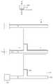
Translated fromKorean도 1은 종래 액정표시패널을 나타내는 사시도이다.1 is a perspective view illustrating a conventional liquid crystal display panel.
도 2는 본 발명의 제1 실시 예에 따른 박막트랜지스터 기판을 나타내는 평면도이다.2 is a plan view illustrating a thin film transistor substrate according to a first exemplary embodiment of the present invention.
도 3은 도 2에 도시된 박막트랜지스터 기판을 선"Ⅰ-Ⅰ'", "Ⅱ-Ⅱ'", "Ⅲ-Ⅲ'"를 따라 절단하여 도시한 단면도이다.3 is a cross-sectional view of the thin film transistor substrate shown in FIG. 2 taken along lines "I-I '", "II-II'", and "III-III '".
도 4a 및 도 4b는 도 2 및 도 3에 도시된 박막트랜지스터 기판의 제1 마스크 공정을 나타내는 평면도 및 단면도이다.4A and 4B are plan views and cross-sectional views illustrating a first mask process of the thin film transistor substrate illustrated in FIGS. 2 and 3.
도 5a 및 도 5b는 도 2 및 도 3에 도시된 박막트랜지스터 기판의 제2 마스크 공정을 나타내는 평면도 및 단면도이다.5A and 5B are plan views and cross-sectional views illustrating a second mask process of the thin film transistor substrate illustrated in FIGS. 2 and 3.
도 6a 및 도 6b는 도 2 및 도 3에 도시된 박막트랜지스터 기판의 제3 마스크 공정을 나타내는 평면도 및 단면도이다.6A and 6B are plan views and cross-sectional views illustrating a third mask process of the thin film transistor substrate illustrated in FIGS. 2 and 3.
도 7a 내지 도 7c는 도 6a 및 도 6b에 도시된 제3 마스크 공정을 상세히 설명하기 위한 단면도이다.7A to 7C are cross-sectional views for describing in detail the third mask process illustrated in FIGS. 6A and 6B.
도 8은 본 발명의 제2 실시 예에 따른 박막트랜지스터 기판을 나타내는 단면 도이다.8 is a cross-sectional view illustrating a thin film transistor substrate according to a second exemplary embodiment of the present invention.
도 9a 내지 도 9d는 도 8에 도시된 박막트랜지스터 기판의 제2 마스크 공정을 상세히 나타내는 단면도이다.9A to 9D are cross-sectional views illustrating in detail a second mask process of the thin film transistor substrate illustrated in FIG. 8.
< 도면의 주요 부분에 대한 부호의 설명 ><Description of Symbols for Main Parts of Drawings>
102 : 게이트 라인104 : 데이터 라인102: gate line 104: data line
106 : 게이트전극108 : 소스전극106: gate electrode 108: source electrode
110 : 드레인전극112 : 게이트절연막110: drain electrode 112: gate insulating film
114 : 활성층116 : 오믹접촉층114: active layer 116: ohmic contact layer
118 : 보호막120 : 반도체 보호막118: protective film 120: semiconductor protective film
122 : 화소전극128 : 스토리지전극122: pixel electrode 128: storage electrode
140 : 스토리지캐패시터150 : 게이트패드140: storage capacitor 150: gate pad
160 : 데이터패드170 : 투명도전막160: data pad 170: transparent conductive film
172 : 게이트금속막172: gate metal film
본 발명은 박막트랜지스터 기판의 제조방법에 관한 것으로, 특히 공정을 단순화시킬 수 있는 박막트랜지스터 기판의 제조 방법에 관한 것이다.The present invention relates to a method for manufacturing a thin film transistor substrate, and more particularly to a method for manufacturing a thin film transistor substrate that can simplify the process.
액정 표시 장치는 전계를 이용하여 액정의 광투과율을 조절함으로써 화상을 표시하게 된다. 이러한 액정 표시 장치는 도 1에 도시된 바와 같이 액정(76)을 사이에 두고 서로 대향하여 합착된 박막 트랜지스터 기판(70) 및 칼러 필터 기판(80)을 구비한다.The liquid crystal display device displays an image by adjusting the light transmittance of the liquid crystal using an electric field. As shown in FIG. 1, the liquid crystal display includes a thin
칼라 필터 기판(80)에는 빛샘 방지를 위한 블랙 매트릭스(68)와, 칼러 구현을 위한 칼러 필터(62), 화소 전극(72)과 수직전계를 이루는 공통전극(64)과, 그들 위에 액정 배향을 위해 도포된 상부 배향막을 포함하는 칼라 필터 어레이가 상부기판(11) 상에 형성된다.The
박막 트랜지스터 기판(70)에는 서로 교차되게 형성된 게이트라인(82) 및 데이터라인(74)과, 그들(82,74)의 교차부에 형성된 박막트랜지스터(58)와, 박막트랜지스터(58)와 접속된 화소 전극(72)과, 그들 위에 액정 배향을 위해 도포된 하부 배향막을 포함하는 박막트랜지스터 어레이가 하부기판(1) 상에 형성된다.The thin
이러한 액정 표시 장치에서 박막 트랜지스터 어레이 기판은 반도체 공정을 포함함과 아울러 다수의 마스크 공정을 필요로 함에 따라 제조 공정이 복잡하여 액정 패널 제조 단가 상승의 중요 원인이 되고 있다. 이는 하나의 마스크 공정이 박막 증착 공정, 세정 공정, 포토리소그래피 공정, 식각 공정, 포토레지스트 박리 공정, 검사 공정 등과 같은 많은 공정을 포함하고 있기 때문이다. 이를 해결하기 위하여, 박막 트랜지스터 어레이 기판은 마스크 공정수를 줄이는 방향으로 발전하고 있다.In such a liquid crystal display device, the thin film transistor array substrate includes a semiconductor process and requires a plurality of mask processes, and thus, the manufacturing process is complicated, which is an important cause of an increase in the manufacturing cost of the liquid crystal panel. This is because one mask process includes many processes such as a thin film deposition process, a cleaning process, a photolithography process, an etching process, a photoresist stripping process, an inspection process, and the like. In order to solve this problem, the thin film transistor array substrate is developing in a direction of reducing the number of mask processes.
따라서, 본 발명의 목적은 마스크 공정 수를 절감할 수 있는 박막트랜지스터 기판의 제조 방법을 제공하는 것이다.Accordingly, it is an object of the present invention to provide a method for manufacturing a thin film transistor substrate which can reduce the number of mask processes.
삭제delete
삭제delete
삭제delete
삭제delete
삭제delete
삭제delete
삭제delete
삭제delete
삭제delete
상기 목적을 달성하기 위하여, 본 발명에 따른 박막트랜지스터 기판의 제조방법은 기판 상에 게이트 금속막과 투명도전막을 적층하는 단계와; 상기 게이트 금속막과 상기 투명 도전막을 패터닝하여 게이트라인, 게이트전극, 상기 게이트 라인과 접속되는 게이트패드 및 데이터패드를 포함하는 게이트패턴들과 화소전극을 제1 마스크 공정으로 형성하는 단계와; 상기 게이트패턴들과 화소전극이 형성된 기판 상에 반도체패턴과 게이트절연패턴을 제2 마스크 공정으로 형성하는 단계와; 상기 게이트 절연 패턴을 마스크로 상기 게이트 패드, 상기 데이터 패드 및 상기 화소 전극의 게이트 금속막을 패터닝하여 상기 게이트 패드, 데이터 패드 및 화소전극의 투명 도전막을 노출시키는 단계와; 상기 반도체패턴 및 게이트절연패턴이 형성된 기판 상에 상기 데이터 패드와 접속되는 데이터라인, 소스전극 및 드레인전극을 포함하는 데이터패턴을 형성하는 제3 마스크 공정으로 형성하는 단계와; 상기 반도체 패턴의 채널 내의 활성층을 산소 또는 질소 플라즈마 중 어느 하나에 노출시킴으로써 상기 반도체 패턴이 노출된 활성층 상에 반도체 보호막을 형성하는 단계를 포함하는 것을 특징으로 한다.In order to achieve the above object, a method of manufacturing a thin film transistor substrate according to the present invention comprises the steps of laminating a gate metal film and a transparent conductive film on the substrate; Patterning the gate metal layer and the transparent conductive layer to form gate patterns including a gate line, a gate electrode, a gate pad and a data pad connected to the gate line, and a pixel electrode in a first mask process; Forming a semiconductor pattern and a gate insulating pattern on a substrate on which the gate patterns and the pixel electrode are formed by a second mask process; Patterning a gate metal film of the gate pad, the data pad, and the pixel electrode using the gate insulating pattern as a mask to expose a transparent conductive film of the gate pad, the data pad, and the pixel electrode; Forming a data pattern including a data line, a source electrode, and a drain electrode connected to the data pad on the substrate on which the semiconductor pattern and the gate insulation pattern are formed; And forming a semiconductor protective film on the active layer to which the semiconductor pattern is exposed by exposing the active layer in the channel of the semiconductor pattern to either oxygen or nitrogen plasma.
상기 화소전극은 상기 게이트 절연 패턴을 사이에 두고 상기 게이트 라인과 상기 데이터 라인이 교차하여 마련된 화소영역에 형성된 상기 투명도전막과, 상기 투명 도전막의 일측 상에 형성되는 상기 게이트 금속막을 포함하는 것을 특징으로 한다.The pixel electrode may include the transparent conductive film formed in a pixel region where the gate line and the data line cross each other with the gate insulating pattern interposed therebetween, and the gate metal film formed on one side of the transparent conductive film. do.
상기 반도체패턴과 게이트절연패턴을 제2 마스크 공정으로 형성하는 단계는 상기 게이트패턴보다 상대적으로 넓은 폭으로 상기 게이트패턴을 따라 상기 반도체패턴과 게이트절연패턴을 형성하는 단계를 포함하는 것을 특징으로 한다.The forming of the semiconductor pattern and the gate insulating pattern by a second mask process may include forming the semiconductor pattern and the gate insulating pattern along the gate pattern with a width wider than that of the gate pattern.
상기 반도체패턴과 게이트절연패턴을 제2 마스크 공정으로 형성하는 단계는 상기 게이트 패턴들과 화소전극이 형성된 기판 상에 게이트 절연막, 제1 및 제2 반도체층을 순차적으로 적층하는 단계와; 상기 게이트 절연막, 제1 및 제2 반도체층을 패터닝하여 동일 패턴의 게이트 절연패턴, 활성층 및 오믹접촉층을 형성하는 단계와; 상기 게이트 절연패턴을 마스크로 이용하여 상기 게이트 금속막을 패터닝하는 단계를 포함하는 것을 특징으로 한다.The forming of the semiconductor pattern and the gate insulating pattern by a second mask process may include sequentially stacking a gate insulating film, first and second semiconductor layers on a substrate on which the gate patterns and the pixel electrode are formed; Patterning the gate insulating layer, the first and second semiconductor layers to form a gate insulating pattern, an active layer, and an ohmic contact layer having the same pattern; Patterning the gate metal layer using the gate insulating pattern as a mask.
상기 반도체패턴과 게이트절연패턴을 제2 마스크 공정으로 형성하는 단계는 상기 게이트 패턴들과 화소전극이 형성된 기판 상에 게이트 절연막, 제1 및 제2 반도체층을 순차적으로 적층하는 단계와; 상기 제2 반도체층 상에 부분 노광 마스크를 이용하여 단차진 포토레지스트 패턴을 형성하는 단계와; 상기 포토레지스트 패턴을 이용하여 상기 게이트 절연막, 제1 및 제2 반도체층을 패터닝하여 게이트 절연패턴, 활성층 및 오믹접촉층을 형성하는 단계와; 상기 포토레지스트 패턴을 에싱하는 단계와; 상기 에싱된 포토레지스트 패턴을 이용하여 박막트랜지스터의 활성층 및 오믹접촉층을 제외한 노출된 활성층 및 오믹접촉층을 제거하는 단계와; 상기 게이트 절연패턴을 마스크로 이용하여 상기 게이트 금속막을 패터닝하는 단계를 포함하는 것을 특징으로 한다.The forming of the semiconductor pattern and the gate insulating pattern by a second mask process may include sequentially stacking a gate insulating film, first and second semiconductor layers on a substrate on which the gate patterns and the pixel electrode are formed; Forming a stepped photoresist pattern on the second semiconductor layer using a partial exposure mask; Patterning the gate insulating layer, the first and the second semiconductor layers using the photoresist pattern to form a gate insulating pattern, an active layer, and an ohmic contact layer; Ashing the photoresist pattern; Removing the exposed active layer and the ohmic contact layer except the active layer and the ohmic contact layer of the thin film transistor using the ashed photoresist pattern; Patterning the gate metal layer using the gate insulating pattern as a mask.
삭제delete
삭제delete
상기 박막트랜지스터 기판의 제조방법은 게이트라인과 게이트 절연패턴을 사이에 두고 중첩되며 상기 화소전극과 접속되어 스토리지캐패시터를 이루는 스토리지 전극을 제3 마스크 공정에서 형성하는 단계를 더 포함하는 것을 특징으로 한다.The method of manufacturing the thin film transistor substrate may further include forming a storage electrode overlapping with the gate line and the gate insulating pattern therebetween and connected to the pixel electrode to form a storage capacitor in a third mask process.
상기 목적 외에 본 발명의 다른 목적 및 이점들은 첨부 도면을 참조한 본 발명의 바람직한 실시 예에 대한 설명을 통하여 명백하게 드러나게 될 것이다.Other objects and advantages of the present invention will become apparent from the following description of preferred embodiments of the present invention with reference to the accompanying drawings.
이하, 본 발명의 바람직한 실시 예들을 도 2 내지 도 9d를 참조하여 상세하게 설명하기로 한다.Hereinafter, exemplary embodiments of the present invention will be described in detail with reference to FIGS. 2 to 9D.
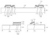
도 2는 본 발명의 제1 실시 예에 따른 액정표시패널의 박막트랜지스터 기판을 나타내는 평면도이고, 도 3은 도 2에서 선Ⅰ-Ⅰ',Ⅱ-Ⅱ', Ⅲ-Ⅲ'를 따라 절취한 박막트랜지스터 기판을 나타내는 단면도이다.FIG. 2 is a plan view illustrating a thin film transistor substrate of a liquid crystal display panel according to a first embodiment of the present invention, and FIG. 3 is a thin film taken along lines I-I ', II-II' and III-III 'of FIG. 2. It is sectional drawing which shows a transistor substrate.
도 2 및 도 3에 도시된 박막트랜지스터 기판은 하부 기판(101) 위에 게이트 절연패턴(112)을 사이에 두고 교차하게 형성된 게이트 라인(102) 및 데이터 라인 (104)과, 그 교차부마다 형성된 박막 트랜지스터(130)와, 그 교차 구조로 마련된 화소 영역(105)에 형성된 화소 전극(122)과, 박막 트랜지스터(130)의 채널을 보호하는 반도체 보호막(120)과, 화소전극(122)과 게이트라인(102)의 중첩부에 형성된 스토리지 캐패시터(140)와, 게이트 라인(102)에서 연장된 게이트 패드(150)와, 데이터 라인(104)에서 연장된 데이터 패드(160)를 구비한다.The thin film transistor substrate shown in FIGS. 2 and 3 includes a
게이트 신호를 공급하는 게이트 라인(102)과 데이터 신호를 공급하는 데이터 라인(104)은 교차 구조로 형성되어 화소 영역(105)을 정의한다.The
박막 트랜지스터(130)는 게이트 라인(102)의 게이트 신호에 응답하여 데이터 라인(104)의 화소 신호가 화소 전극(122)에 충전되어 유지되게 한다. 이를 위하여, 박막 트랜지스터(130)는 게이트 라인(102)에 접속된 게이트 전극(106)과, 데이터 라인(104)에 접속된 소스 전극(108)과, 화소 전극(122)에 접속된 드레인 전극(110)을 구비한다. 또한, 박막 트랜지스터(130)는 게이트 전극(106)과 게이트 절연패턴(112)을 사이에 두고 중첩되면서 소스 전극(108)과 드레인 전극(110) 사이에 채널을 형성하는 반도체패턴(114,116)을 구비한다.The
게이트전극(106)과 게이트라인(102)을 포함하는 게이트패턴은 투명도전막(170)과, 그 투명도전막(170) 상에 게이트금속막(172)이 적층된 구조로 형성된다.The gate pattern including the
반도체패턴은 소스전극(108)과 드레인전극(110) 사이의 채널을 형성하고, 게이트절연패턴(112)을 사이에 두고 게이트패턴과 부분적으로 중첩되게 형성된 활성층(114)을 구비한다. 그리고, 반도체패턴은 활성층(114) 위에 형성되어 스토리지전극(128), 소스전극(108) 및 드레인전극(110)과 오믹접촉을 위한 오믹접촉층(116) 을 추가로 구비한다.The semiconductor pattern includes an
반도체 보호막(120)은 소스 전극(108) 및 드레인 전극(110) 사이에 채널을 형성하는 활성층(114) 상에 산화실리콘(SiOx) 또는 질화실리콘(SiNx)으로 형성된다. 이 반도체 보호막(120)은 소스 전극(108) 및 드레인 전극(110) 사이의 채널을 이루는 활성층(114)이 노출되는 것을 방지한다. 또한, 반도체 보호막(120)은 게이트 절연패턴(112)을 사이에 두고 게이트라인(102)을 따라 형성되는 활성층(114)이 노출되는 것을 방지한다.The
화소 전극(122)은 박막 트랜지스터(130)의 드레인 전극(110)과 직접 접속되어 화소 영역(105)에 형성된다. 화소전극(122)은 화소영역(105)에 형성된 투명도전막(170)과, 반도체 패턴과 중첩되는 영역의 상기 투명도전막(170) 상에 형성되는 게이트금속막(172)으로 형성된다. 화소 전극(122)의 게이트 금속막(172)은 도전율이 상대적으로 높아 투명 도전막(170)의 저항성분을 보상한다.The
이에 따라, 박막 트랜지스터(130)를 통해 화소 신호가 공급된 화소 전극(122)과 기준 전압이 공급된 공통 전극(도시하지 않음) 사이에는 전계가 형성된다. 이러한 전계에 의해 칼라 필터 기판과 박막트랜지스터 기판 사이의 액정 분자들이 유전 이방성에 의해 회전하게 된다. 그리고, 액정 분자들의 회전 정도에 따라 화소 영역(105)을 투과하는 광 투과율이 달라지게 됨으로써 계조를 구현하게 된다.Accordingly, an electric field is formed between the
스토리지 캐패시터(140)는 게이트라인(102)과, 그 게이트라인(102)과 게이트절연패턴(112), 활성층(114) 및 오믹접촉층(116)을 사이에 두고 중첩되며 화소전극(122)과 접속된 스토리지전극(128)으로 구성된다. 이러한 스토리지 캐패시터(140) 는 화소 전극(122)에 충전된 화소 신호가 다음 화소 신호가 충전될 때까지 안정적으로 유지되게 한다.The
게이트패드(150)는 게이트 드라이버(도시하지 않음)와 접속되어 게이트 드라이버에서 생성된 게이트신호를 게이트라인(102)에 공급한다. 이러한 게이트 패드(150)는 게이트라인(102)으로부터 신장된 투명도전막(170)이 노출된 구조로 형성된다.The
데이터패드(160)는 데이터 드라이버(도시하지 않음)와 접속되어 데이터 드라이버에서 생성된 데이터신호를 데이터라인(104)에 공급한다. 이러한 데이터패드(160)는 투명 도전막(170)과, 그 투명 도전막(170) 상에 데이터라인(104)과 중첩되는 영역에 형성되는 게이트 금속막(172)으로 형성된다. 이 데이터 패드(160)의 게이트 금속막(172)은 도전율이 상대적으로 높아 투명 도전막(170)의 저항성분을 보상한다. 이러한 데이터 패드(160)의 게이트 금속막(172)과 데이터라인(104) 사이에는 게이트절연패턴(112), 활성층(114) 및 오믹접촉층(116)이 형성된다.The
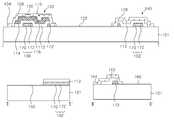
도 4a 및 도 4b는 본 발명의 제1 실시 예에 따른 박막 트랜지스터 어레이 기판의 제조 방법 중 제1 마스크 공정을 설명하기 위한 평면도 및 단면도이다.4A and 4B are plan and cross-sectional views illustrating a first mask process in the method of manufacturing the thin film transistor array substrate according to the first embodiment of the present invention.
도 4a 및 도 4b에 도시된 바와 같이 제1 마스크 공정으로 하부 기판(101) 상에 화소전극(122)과; 2층 구조의 게이트 라인(102), 게이트 전극(106),게이트 패드(150), 데이터패드(160)를 포함하는 게이트패턴이 형성된다.A
이를 위해, 하부기판(101) 상에 스퍼터링 등의 증착방법을 통해 투명도전막(170)과 게이트금속막(172)이 순차적으로 형성된다. 여기서, 투명도전막(170)은 인듐 틴 옥사이드(Indium Tin Oxide : ITO), 틴 옥사이드(Tin Oxide : TO), 인듐 틴 징크 옥사이드(Indium Tin Zinc Oxide : ITZO), 인듐 징크 옥사이드(Indium Zinc Oxide : IZO)등과 같은 투명도전성물질이 이용되고, 게이트금속막(172)은 알루미늄/네오듐(AlNd)을 포함하는 알루미늄(Al)계 금속, 몰리브덴(Mo), 구리(Cu), 크롬(Cr), 탄탈(Ta), 티타늄(Ti) 등과 같은 금속이 이용된다. 이어서, 투명도전막(170)과 게이트 금속층(172)이 제1 마스크를 이용한 포토리소그래피공정과 식각공정에 의해 패터닝됨으로써 2층 구조의 게이트 라인(102) 및 게이트 전극(106)과; 게이트금속막(172)을 포함하는 게이트 패드(150), 데이터패드(160) 및 화소전극(122)이 형성된다.To this end, the transparent
도 5a 및 도 5b는 본 발명의 제1 실시 예에 따른 박막 트랜지스터 어레이 기판의 제조 방법 중 제2 마스크 공정을 설명하기 위한 평면도 및 단면도이다.5A and 5B are plan views and cross-sectional views illustrating a second mask process in the method of manufacturing the thin film transistor array substrate according to the first embodiment of the present invention.
도 5a 및 도 5b에 도시된 바와 같이 제2 마스크공정으로 게이트패턴이 형성된 하부기판(101) 상에 게이트절연패턴(112)과; 활성층(114) 및 오믹접촉층(116)을 포함하는 반도체패턴이 형성된다.A
이를 위해, 게이트패턴이 형성된 하부 기판(101) 상에 PECVD, 스퍼터링 등의 증착 방법을 통해 게이트 절연막과 제1 및 제2 반도체층이 순차적으로 형성된다. 여기서, 게이트 절연막의 재료로는 산화 실리콘(SiOx) 또는 질화 실리콘(SiNx) 등의 무기 절연 물질이 이용되며, 제1 반도체층은 불순물이 도핑되지 않은 비정질실리콘이 이용되며, 제2 반도체층은 N형 또는 P형의 불순물이 도핑된 비정질실리콘이 이용된다. 이어서, 제1 및 제2 반도체층과 게이트절연막이 제2 마스크를 이용한 포토리소그래피공정과 식각공정에 의해 패터닝됨으로써 게이트라인(102) 및 게이트전극(106)과 중첩되는 게이트절연패턴(112)과, 그 게이트절연패턴(112) 상에 활성층(114) 및 오믹접촉층(116)을 포함하는 반도체패턴이 형성된다.To this end, the gate insulating film and the first and second semiconductor layers are sequentially formed on the
그런 다음, 게이트 절연 패턴(112)을 마스크로 이용하여 데이터패드(160), 게이트패드(150) 및 화소전극(122)의 노출된 게이트 금속막(172)이 제거됨으로써 데이터패드(160), 게이트패드(150) 및 화소전극(122)에 포함된 투명도전막(170)이 노출된다.Next, the exposed
도 6a 및 도 6b는 본 발명의 제1 실시 예에 따른 박막 트랜지스터 어레이 기판의 제조 방법 중 제3 마스크 공정을 설명하기 위한 평면도 및 단면도이다.6A and 6B are plan views and cross-sectional views illustrating a third mask process in the method of manufacturing the thin film transistor array substrate according to the first embodiment of the present invention.
도 6a 및 도 6b에 도시된 바와 같이 제3 마스크 공정으로 게이트절연패턴(112)과 반도체패턴이 형성된 하부 기판(101) 상에 데이터라인(104), 소스전극(108), 드레인전극(110), 스토리지전극(128)을 포함하는 데이터패턴과; 소스(108) 및 드레인 전극(110) 사이의 채널을 보호하는 반도체 보호막(120)이 형성된다. 이러한 제3 마스크공정을 도 7a 내지 도 7c를 참조하여 상세히 하면 다음과 같다.6A and 6B, the
도 7a에 도시된 바와 같이 반도체패턴이 형성된 하부기판(101) 상에 스퍼터링 등의 증착 방법을 데이터금속층(109)이 순차적으로 형성된다. 여기서, 데이터금속층(109)은 몰리브덴(Mo), 구리(Cu) 등과 같은 금속으로 이루어진다.As shown in FIG. 7A, the
이 데이터 금속층(109)이 포토리소그래피공정과 식각공정에 의해 패터닝됨으로써 도 7b에 도시된 바와 같이 스토리지전극(128), 데이터 라인(104), 소스전극(108) 및 드레인 전극(110)을 포함하는 데이터패턴이 형성된다.The
그리고, 데이터 패턴을 마스크로 이용한 건식 식각 공정으로 노출된 오믹접촉층(116)이 제거됨으로써 박막트랜지스터(130)의 채널을 이루는 활성층(114)과 게이트라인(102) 상의 활성층(114)이 노출된다.In addition, the
그런 다음, 노출된 활성층(114) 표면은 도 7c에 도시된 바와 같이 Ox(예를 들어, O2) 또는 Nx(예를 들어, N2) 플라즈마에 노출된다. 그러면, 이온 상태의 Ox 또는 Nx는 활성층(114)에 포함된 실리콘(Si)과 반응함으로써 활성층(114) 상에는 SiO2 및 SiNx 중 어느 하나로 이루어진 반도체 보호막(120)이 형성된다. 특히, 반도체 보호막(120)은 후속공정인 세정공정시 이용되는 세정액 등에 노출되는 채널부의 활성층(114)의 손상을 방지하게 된다.The exposed
도 8은 본 발명의 제2 실시 예에 따른 박막트랜지스터 기판을 나타내는 단면도이다.8 is a cross-sectional view illustrating a thin film transistor substrate according to a second exemplary embodiment of the present invention.
도 8을 참조하면, 본 발명의 제2 실시 예에 따른 박막트랜지스터 기판은 도 3에 도시된 박막트랜지스터 기판과 대비하여 게이트라인(102), 데이터 패드(160) 및 스토리지 캐패시터(140)를 제외한 박막트랜지스터(130)에 형성되는 반도체 패턴을 제외하고는 동일한 구성요소를 구비한다. 이에 따라, 동일한 구성요소에 대한 상세한 설명은 생략하기로 한다.Referring to FIG. 8, the thin film transistor substrate according to the second embodiment of the present invention is thin film except for the
스토리지 캐패시터(140)는 게이트라인(102)과, 그 게이트라인(102)과 게이트절연패턴(112)을 사이에 두고 중첩되며 화소전극(122)과 접속된 스토리지전극(128)으로 구성된다. 이러한 스토리지 캐패시터(140)는 화소 전극(122)에 충전된 화소 신호가 다음 화소 신호가 충전될 때까지 안정적으로 유지되게 한다. 도 8에 도시된 스토리지 캐패시터(140)는 도 3에 도시된 스토리지 캐패시터에 비해 스토리지 하부 전극인 게이트라인(102)과 스토리지 상부 전극인 스토리지 전극(128) 간의 거리가 가까워 용량값이 상대적으로 크다.The
데이터패드(160)는 데이터 드라이버(도시하지 않음)와 접속되어 데이터 드라이버에서 생성된 데이터신호를 데이터라인(104)에 공급한다. 이러한 데이터패드(160)는 투명 도전막(170)과, 그 투명 도전막(170) 상에 데이터라인(104)과 중첩되는 영역에 형성되는 게이트 금속막(172)으로 형성된다. 이 데이터 패드(160)의 게이트 금속막(172)은 도전율이 상대적으로 높아 투명 도전막(170)의 저항성분을 보상한다. 이러한 데이터 패드(160)의 게이트 금속막(172)은 게이트 절연패턴을 사이에 두고 데이터라인(104)과 중첩된다.The
이와 같이, 본 발명의 제2 실시 예에 따른 박막트랜지스터 기판은 반도체 패턴이 게이트 전극과 중첩되는 게이트 절연패턴 상에 형성되므로 반도체 보호막도 채널 영역에만 형성된다.As described above, the thin film transistor substrate according to the second embodiment of the present invention is formed on the gate insulating pattern in which the semiconductor pattern overlaps with the gate electrode, and thus the semiconductor passivation layer is also formed only in the channel region.
도 9a 내지 도 9d는 도 8에 도시된 박막트랜지스터 기판의 제2 마스크 공정을 설명하기 위한 단면도이다.9A to 9D are cross-sectional views for describing a second mask process of the thin film transistor substrate illustrated in FIG. 8.
도 9a에 도시된 바와 같이 게이트 패턴이 형성된 하부기판(101) 상에 스퍼터링 등의 증착 방법을 게이트 절연막(220), 제1 및 제2 반도체층(222,226)과 포토레지스트막(228)이 순차적으로 형성된다.As illustrated in FIG. 9A, the
그런 다음, 부분 노광 마스크인 제2 마스크가 하부기판(101) 상부에 정렬된 다. 제2 마스크는 투명한 재질인 마스크 기판과, 마스크 기판의 차단 영역에 형성된 차단부와, 마스크 기판의 부분 노광 영역에 형성된 회절 노광부(또는 반투과부)를 구비한다. 여기서, 마스크 기판이 노출된 영역은 노광 영역이 된다. 이러한 제2 마스크를 이용한 포토레지스트막(228)을 노광한 후 현상함으로써 도 9b에 도시된 바와 같이 제2 마스크의 차단부와 회절 노광부에 대응하여 차단 영역과 부분 노광 영역에서 단차를 갖는 포토레지스트 패턴(230)이 형성된다. 즉, 부분 노광 영역(S3)에 형성된 포토레지스트 패턴(230)은 차단 영역에서 형성된 제1 높이를 갖는 포토레지스트 패턴(230)보다 낮은 제2 높이를 갖게 된다.Then, the second mask, which is the partial exposure mask, is aligned above the
이러한 포토레지스트 패턴(230)을 마스크로 이용한 건식 식각 공정으로 게이트 절연막(220), 제1 및 제2 반도체층(222,226)이 패터닝됨으로써 동일 패턴의 게이트 절연패턴(112), 활성층(114) 및 오믹접촉층(116)이 형성된다.The
이어서, 산소(O2) 플라즈마를 이용한 애싱(Ashing) 공정으로 부분 노광 영역(S3)에 제2 높이를 갖는 포토레지스트 패턴(230)은 도 9c에 도시된 바와 같이 제거되고, 차단 영역(S2)에 제1 높이(h1)를 갖는 포토레지스트 패턴(230)은 높이가 낮아진 상태가 된다. 이러한 포토레지스트 패턴(230)을 이용한 식각 공정으로 부분 노광 영역, 즉 박막 트랜지스터(130)의 채널부를 제외한 나머지 영역 상에 형성된 활성층(114) 및 오믹접촉층(116)이 제거된다.Subsequently, the
그리고, 반도체 패턴 위에 남아 있던 포토레지스트 패턴(230)은 도 9d에 도시된 바와 같이 스트립 공정으로 제거된다.The
상술한 바와 같이, 본 발명에 따른 박막트랜지스터 기판의 제조방법은 제1 마스크공정으로 화소전극과 게이트패턴을 형성하고, 제2 마스크공정으로 반도체패턴을 형성하고, 제3 마스크공정으로 데이터패턴을 형성되어 박막트랜지스터 어레이 기판이 완성된다. 이와 같이 박막트랜지스터 어레이 기판을 리프트 오프 공정 또는 패드 오픈 공정 없이 3마스크공정으로 형성함으로써 구조 및 제조공정이 단순화되고 제조단가를 절감할 수 있음과 아울러 제조수율이 향상된다.As described above, in the method of manufacturing the thin film transistor substrate according to the present invention, the pixel electrode and the gate pattern are formed by the first mask process, the semiconductor pattern is formed by the second mask process, and the data pattern is formed by the third mask process. Thus, the thin film transistor array substrate is completed. Thus, by forming the thin film transistor array substrate in a three mask process without a lift-off process or a pad open process, the structure and manufacturing process can be simplified, manufacturing cost can be reduced, and manufacturing yield can be improved.
또한, 본 발명에 따른 박막트랜지스터 어레이 기판의 제조방법은 박막트랜지스터의 채널과 대응되는 노출된 활성층을 별도의 보호막 없이 반도체 보호막을 이용하여 보호하게 된다. 이에 따라, 종래 보호막을 형성하기 위한 증착장비 또는 코팅장비가 불필요하여 제조비용을 절감할 수 있으며 종래 드레인전극을 노출시키는 콘택홀의 단차부에서 발생되는 화소전극의 오픈을 방지할 수 있다.In addition, the method for manufacturing a thin film transistor array substrate according to the present invention is to protect the exposed active layer corresponding to the channel of the thin film transistor using a semiconductor protective film without a separate protective film. Accordingly, the deposition cost or the coating equipment for forming the conventional passivation layer is unnecessary, thereby reducing the manufacturing cost and preventing the opening of the pixel electrode generated at the step portion of the contact hole exposing the conventional drain electrode.
이상 설명한 내용을 통해 당업자라면 본 발명의 기술사상을 일탈하지 아니하는 범위에서 다양한 변경 및 수정이 가능함을 알 수 있을 것이다. 따라서, 본 발명의 기술적 범위는 명세서의 상세한 설명에 기재된 내용으로 한정되는 것이 아니라 특허 청구의 범위에 의해 정하여져야만 할 것이다.Those skilled in the art will appreciate that various changes and modifications can be made without departing from the technical spirit of the present invention. Therefore, the technical scope of the present invention should not be limited to the contents described in the detailed description of the specification but should be defined by the claims.
Claims (17)
Translated fromKoreanPriority Applications (4)
| Application Number | Priority Date | Filing Date | Title |
|---|---|---|---|
| KR1020050058058AKR101127836B1 (en) | 2005-06-30 | 2005-06-30 | Method of Fabricating Thin Film Transistor Substrate |
| CNB2005100230945ACN100447643C (en) | 2005-06-30 | 2005-12-26 | Thin film transistor substrate and manufacturing method thereof |
| JP2005376179AJP4578402B2 (en) | 2005-06-30 | 2005-12-27 | Thin film transistor substrate and manufacturing method thereof |
| US11/320,510US7504661B2 (en) | 2005-06-30 | 2005-12-28 | Thin film transistor substrate and fabricating method thereof |
Applications Claiming Priority (1)
| Application Number | Priority Date | Filing Date | Title |
|---|---|---|---|
| KR1020050058058AKR101127836B1 (en) | 2005-06-30 | 2005-06-30 | Method of Fabricating Thin Film Transistor Substrate |
Publications (2)
| Publication Number | Publication Date |
|---|---|
| KR20070002497A KR20070002497A (en) | 2007-01-05 |
| KR101127836B1true KR101127836B1 (en) | 2012-03-21 |
Family
ID=37588390
Family Applications (1)
| Application Number | Title | Priority Date | Filing Date |
|---|---|---|---|
| KR1020050058058AExpired - LifetimeKR101127836B1 (en) | 2005-06-30 | 2005-06-30 | Method of Fabricating Thin Film Transistor Substrate |
Country Status (4)
| Country | Link |
|---|---|
| US (1) | US7504661B2 (en) |
| JP (1) | JP4578402B2 (en) |
| KR (1) | KR101127836B1 (en) |
| CN (1) | CN100447643C (en) |
Families Citing this family (10)
| Publication number | Priority date | Publication date | Assignee | Title |
|---|---|---|---|---|
| KR101183361B1 (en)* | 2006-06-29 | 2012-09-14 | 엘지디스플레이 주식회사 | Array substrate for LCD and the fabrication method thereof |
| KR101291318B1 (en)* | 2006-11-21 | 2013-07-30 | 삼성디스플레이 주식회사 | Thin film transistor substrate and method for fabricating the same |
| TWI425639B (en)* | 2007-10-22 | 2014-02-01 | Au Optronics Corp | Thin film transistor and manufacturing method thereof |
| CN101556415B (en)* | 2008-04-10 | 2011-05-11 | 北京京东方光电科技有限公司 | Pixel structure and preparation method thereof |
| JP5771365B2 (en)* | 2009-11-23 | 2015-08-26 | 三星ディスプレイ株式會社Samsung Display Co.,Ltd. | Medium and small liquid crystal display |
| WO2011070901A1 (en)* | 2009-12-11 | 2011-06-16 | Semiconductor Energy Laboratory Co., Ltd. | Semiconductor device and manufacturing method thereof |
| KR101948168B1 (en)* | 2011-12-08 | 2019-04-26 | 엘지디스플레이 주식회사 | Narrow bezel type liquid crystal display device |
| CN102543866B (en)* | 2012-03-06 | 2013-08-28 | 深圳市华星光电技术有限公司 | Manufacturing method of array substrate of penetration type liquid crystal display(LCD) |
| CN103828388A (en)* | 2012-08-17 | 2014-05-28 | 弗莱克斯电子有限责任公司 | Methods and displays for providing intelligent television badges |
| CN104992950A (en)* | 2015-06-05 | 2015-10-21 | 京东方科技集团股份有限公司 | Array substrate and preparation method thereof, and display device |
Citations (4)
| Publication number | Priority date | Publication date | Assignee | Title |
|---|---|---|---|---|
| JPH0219840A (en)* | 1988-07-08 | 1990-01-23 | Hitachi Ltd | Active matrix panel and its manufacturing method |
| JP2002176062A (en)* | 2000-02-04 | 2002-06-21 | Matsushita Electric Ind Co Ltd | Method of manufacturing substrate for display device |
| US20040109101A1 (en)* | 2002-12-04 | 2004-06-10 | Lg. Philips Lcd Co., Ltd. | Liquid crystal display device and manufacturing method thereof |
| US20050078264A1 (en)* | 2003-10-14 | 2005-04-14 | Lg Philips Lcd Co., Ltd. | Thin film transistor array substrate, method of fabricating the same, liquid crystal display panel having the same and fabricating method thereof |
Family Cites Families (17)
| Publication number | Priority date | Publication date | Assignee | Title |
|---|---|---|---|---|
| US5032883A (en)* | 1987-09-09 | 1991-07-16 | Casio Computer Co., Ltd. | Thin film transistor and method of manufacturing the same |
| JPH069246B2 (en)* | 1987-11-02 | 1994-02-02 | 日本電気株式会社 | Method of manufacturing thin film transistor |
| JPH02237161A (en)* | 1989-03-10 | 1990-09-19 | Fujitsu Ltd | Thin-film transistor and its manufacture |
| JPH03116778A (en)* | 1989-09-28 | 1991-05-17 | Matsushita Electric Ind Co Ltd | Manufacture of active matrix substrate and manufacture of display device |
| KR100276442B1 (en)* | 1998-02-20 | 2000-12-15 | 구본준 | Liquid crystal display device and its fabrication method |
| KR100500684B1 (en)* | 1999-12-29 | 2005-07-12 | 비오이 하이디스 테크놀로지 주식회사 | Method for fabricating liquid crystal display using 4-mask process |
| US6476415B1 (en)* | 2000-07-20 | 2002-11-05 | Three-Five Systems, Inc. | Wafer scale processing |
| US20030164908A1 (en)* | 2002-03-01 | 2003-09-04 | Chi Mei Optoelectronics Corp. | Thin film transistor panel |
| CN1333432C (en)* | 2003-08-21 | 2007-08-22 | 广辉电子股份有限公司 | Manufacturing method of thin film transistor array substrate |
| US7220611B2 (en)* | 2003-10-14 | 2007-05-22 | Lg.Philips Lcd Co., Ltd. | Liquid crystal display panel and fabricating method thereof |
| US7760317B2 (en)* | 2003-10-14 | 2010-07-20 | Lg Display Co., Ltd. | Thin film transistor array substrate and fabricating method thereof, liquid crystal display using the same and fabricating method thereof, and method of inspecting liquid crystal display |
| KR100558714B1 (en)* | 2003-10-14 | 2006-03-10 | 엘지.필립스 엘시디 주식회사 | LCD panel and manufacturing method thereof |
| CN100371813C (en)* | 2003-10-14 | 2008-02-27 | Lg.菲利浦Lcd株式会社 | Liquid crystal display panel in in-plane switching liquid crystal display device and manufacturing method thereof |
| KR100583311B1 (en)* | 2003-10-14 | 2006-05-25 | 엘지.필립스 엘시디 주식회사 | LCD panel and manufacturing method thereof |
| KR101107245B1 (en)* | 2004-12-24 | 2012-01-25 | 엘지디스플레이 주식회사 | Horizontal field thin film transistor substrate and its manufacturing method |
| KR101107246B1 (en)* | 2004-12-24 | 2012-01-25 | 엘지디스플레이 주식회사 | Thin film transistor substrate and its manufacturing method |
| CN1313876C (en)* | 2005-01-19 | 2007-05-02 | 广辉电子股份有限公司 | Manufacturing method of pixel structure of thin film transistor liquid crystal display |
- 2005
- 2005-06-30KRKR1020050058058Apatent/KR101127836B1/ennot_activeExpired - Lifetime
- 2005-12-26CNCNB2005100230945Apatent/CN100447643C/ennot_activeExpired - Fee Related
- 2005-12-27JPJP2005376179Apatent/JP4578402B2/ennot_activeExpired - Fee Related
- 2005-12-28USUS11/320,510patent/US7504661B2/enactiveActive
Patent Citations (4)
| Publication number | Priority date | Publication date | Assignee | Title |
|---|---|---|---|---|
| JPH0219840A (en)* | 1988-07-08 | 1990-01-23 | Hitachi Ltd | Active matrix panel and its manufacturing method |
| JP2002176062A (en)* | 2000-02-04 | 2002-06-21 | Matsushita Electric Ind Co Ltd | Method of manufacturing substrate for display device |
| US20040109101A1 (en)* | 2002-12-04 | 2004-06-10 | Lg. Philips Lcd Co., Ltd. | Liquid crystal display device and manufacturing method thereof |
| US20050078264A1 (en)* | 2003-10-14 | 2005-04-14 | Lg Philips Lcd Co., Ltd. | Thin film transistor array substrate, method of fabricating the same, liquid crystal display panel having the same and fabricating method thereof |
Also Published As
| Publication number | Publication date |
|---|---|
| US7504661B2 (en) | 2009-03-17 |
| KR20070002497A (en) | 2007-01-05 |
| JP4578402B2 (en) | 2010-11-10 |
| CN100447643C (en) | 2008-12-31 |
| JP2007013083A (en) | 2007-01-18 |
| US20070001170A1 (en) | 2007-01-04 |
| CN1892373A (en) | 2007-01-10 |
Similar Documents
| Publication | Publication Date | Title |
|---|---|---|
| US7960199B2 (en) | Thin film transistor (TFT) array substrate and fabricating method thereof that protect the TFT and a pixel electrode without a protective film | |
| US9035312B2 (en) | TFT array substrate and fabrication method thereof | |
| KR100456151B1 (en) | Thin film transistor array substrate and method of manufacturing the same | |
| KR100480333B1 (en) | Array substrate for a liquid crystal display device and Method for fabricating of the same | |
| US20060290864A1 (en) | Horizontal electric field switching liquid crystal display device and fabricating method thereof | |
| KR100886241B1 (en) | Manufacturing method of liquid crystal display device | |
| KR20070111029A (en) | Thin film transistor substrate and manufacturing method thereof | |
| KR100558714B1 (en) | LCD panel and manufacturing method thereof | |
| KR101127836B1 (en) | Method of Fabricating Thin Film Transistor Substrate | |
| US6958788B2 (en) | Liquid crystal display device and method of fabricating the same | |
| US20050133787A1 (en) | Thin film transistor array substrate and fabricating method thereof | |
| KR100558717B1 (en) | Horizontal field applied liquid crystal display panel and manufacturing method thereof | |
| KR100637061B1 (en) | Horizontal field applied liquid crystal display panel and manufacturing method thereof | |
| KR101231842B1 (en) | Thin film transistor array substrate and fabricating method thereof | |
| KR20050035645A (en) | Liquid crystal display panel apparatus of horizontal electronic field applying type and fabricating method thereof | |
| KR100625030B1 (en) | Manufacturing method of liquid crystal display device | |
| KR101149939B1 (en) | Thin Film Transistor Substrate And Method Of Fabricating The Same | |
| KR20040061206A (en) | Liquid Crystal Display Panel and Fabricating Method Thereof | |
| KR20080062124A (en) | Thin film transistor substrate and manufacturing method thereof | |
| KR20090108285A (en) | Method of manufacturing thin film transistor substrate | |
| KR20040077313A (en) | Thin Film Transistor Array Substrate And Fabricating Method Thereof |
Legal Events
| Date | Code | Title | Description |
|---|---|---|---|
| PA0109 | Patent application | Patent event code:PA01091R01D Comment text:Patent Application Patent event date:20050630 | |
| PG1501 | Laying open of application | ||
| A201 | Request for examination | ||
| PA0201 | Request for examination | Patent event code:PA02012R01D Patent event date:20100623 Comment text:Request for Examination of Application Patent event code:PA02011R01I Patent event date:20050630 Comment text:Patent Application | |
| PE0902 | Notice of grounds for rejection | Comment text:Notification of reason for refusal Patent event date:20110726 Patent event code:PE09021S01D | |
| E701 | Decision to grant or registration of patent right | ||
| PE0701 | Decision of registration | Patent event code:PE07011S01D Comment text:Decision to Grant Registration Patent event date:20120208 | |
| GRNT | Written decision to grant | ||
| PR0701 | Registration of establishment | Comment text:Registration of Establishment Patent event date:20120312 Patent event code:PR07011E01D | |
| PR1002 | Payment of registration fee | Payment date:20120313 End annual number:3 Start annual number:1 | |
| PG1601 | Publication of registration | ||
| FPAY | Annual fee payment | Payment date:20150227 Year of fee payment:4 | |
| PR1001 | Payment of annual fee | Payment date:20150227 Start annual number:4 End annual number:4 | |
| FPAY | Annual fee payment | Payment date:20160226 Year of fee payment:5 | |
| PR1001 | Payment of annual fee | Payment date:20160226 Start annual number:5 End annual number:5 | |
| PR1001 | Payment of annual fee | Payment date:20170215 Start annual number:6 End annual number:6 | |
| FPAY | Annual fee payment | Payment date:20180213 Year of fee payment:7 | |
| PR1001 | Payment of annual fee | Payment date:20180213 Start annual number:7 End annual number:7 | |
| PR1001 | Payment of annual fee | Payment date:20190215 Start annual number:8 End annual number:8 | |
| FPAY | Annual fee payment | Payment date:20200219 Year of fee payment:9 | |
| PR1001 | Payment of annual fee | Payment date:20200219 Start annual number:9 End annual number:9 | |
| PR1001 | Payment of annual fee | Payment date:20210215 Start annual number:10 End annual number:10 | |
| PR1001 | Payment of annual fee | Payment date:20220210 Start annual number:11 End annual number:11 | |
| PR1001 | Payment of annual fee | Payment date:20230215 Start annual number:12 End annual number:12 | |
| PR1001 | Payment of annual fee | Payment date:20240215 Start annual number:13 End annual number:13 | |
| PR1001 | Payment of annual fee | Payment date:20250218 Start annual number:14 End annual number:14 |