KR101123705B1 - Semiconductor manufacturing apparatus and semiconductor manufacturing method - Google Patents
Semiconductor manufacturing apparatus and semiconductor manufacturing methodDownload PDFInfo
- Publication number
- KR101123705B1 KR101123705B1KR1020090023061AKR20090023061AKR101123705B1KR 101123705 B1KR101123705 B1KR 101123705B1KR 1020090023061 AKR1020090023061 AKR 1020090023061AKR 20090023061 AKR20090023061 AKR 20090023061AKR 101123705 B1KR101123705 B1KR 101123705B1
- Authority
- KR
- South Korea
- Prior art keywords
- substrate
- nozzle
- plating
- liquid
- supply
- Prior art date
- Legal status (The legal status is an assumption and is not a legal conclusion. Google has not performed a legal analysis and makes no representation as to the accuracy of the status listed.)
- Active
Links
- 239000004065semiconductorSubstances0.000titleclaimsabstractdescription51
- 238000004519manufacturing processMethods0.000titleclaimsabstractdescription43
- 239000000758substrateSubstances0.000claimsabstractdescription343
- 239000007788liquidSubstances0.000claimsabstractdescription228
- 238000007747platingMethods0.000claimsabstractdescription228
- 238000000034methodMethods0.000claimsabstractdescription175
- 230000008569processEffects0.000claimsabstractdescription152
- 238000012545processingMethods0.000claimsabstractdescription77
- 230000007246mechanismEffects0.000claimsabstractdescription64
- 238000004140cleaningMethods0.000claimsdescription65
- 230000002093peripheral effectEffects0.000claimsdescription40
- 239000012530fluidSubstances0.000description123
- XLYOFNOQVPJJNP-UHFFFAOYSA-NwaterSubstancesOXLYOFNOQVPJJNP-UHFFFAOYSA-N0.000description63
- 238000007772electroless platingMethods0.000description42
- 238000012546transferMethods0.000description25
- 238000010438heat treatmentMethods0.000description18
- 229910052751metalInorganic materials0.000description18
- 239000002184metalSubstances0.000description18
- 239000010949copperSubstances0.000description17
- 238000006243chemical reactionMethods0.000description14
- 238000001816coolingMethods0.000description14
- 238000001035dryingMethods0.000description12
- 239000000243solutionSubstances0.000description11
- 230000004048modificationEffects0.000description10
- 238000012986modificationMethods0.000description10
- RYGMFSIKBFXOCR-UHFFFAOYSA-NCopperChemical compound[Cu]RYGMFSIKBFXOCR-UHFFFAOYSA-N0.000description9
- 239000006227byproductSubstances0.000description9
- 229910052802copperInorganic materials0.000description9
- 238000010586diagramMethods0.000description9
- 230000006870functionEffects0.000description8
- 239000007789gasSubstances0.000description7
- 238000009825accumulationMethods0.000description6
- 230000000694effectsEffects0.000description5
- KRHYYFGTRYWZRS-UHFFFAOYSA-NFluoraneChemical compoundFKRHYYFGTRYWZRS-UHFFFAOYSA-N0.000description4
- 238000003825pressingMethods0.000description4
- 238000003860storageMethods0.000description4
- 239000000126substanceSubstances0.000description4
- 238000005406washingMethods0.000description4
- 239000000463materialSubstances0.000description3
- 229910052721tungstenInorganic materials0.000description3
- IJGRMHOSHXDMSA-UHFFFAOYSA-NAtomic nitrogenChemical compoundN#NIJGRMHOSHXDMSA-UHFFFAOYSA-N0.000description2
- 230000004888barrier functionEffects0.000description2
- 229910001873dinitrogenInorganic materials0.000description2
- 230000001965increasing effectEffects0.000description2
- 238000012423maintenanceMethods0.000description2
- 238000002156mixingMethods0.000description2
- 238000005192partitionMethods0.000description2
- 238000001556precipitationMethods0.000description2
- 230000001105regulatory effectEffects0.000description2
- 238000006467substitution reactionMethods0.000description2
- 239000002344surface layerSubstances0.000description2
- QPLDLSVMHZLSFG-UHFFFAOYSA-NCopper oxideChemical compound[Cu]=OQPLDLSVMHZLSFG-UHFFFAOYSA-N0.000description1
- 239000005751Copper oxideSubstances0.000description1
- 240000001973Ficus microcarpaSpecies0.000description1
- CPJYFACXEHYLFS-UHFFFAOYSA-N[B].[W].[Co]Chemical compound[B].[W].[Co]CPJYFACXEHYLFS-UHFFFAOYSA-N0.000description1
- FEBFYWHXKVOHDI-UHFFFAOYSA-N[Co].[P][W]Chemical compound[Co].[P][W]FEBFYWHXKVOHDI-UHFFFAOYSA-N0.000description1
- 230000002378acidificating effectEffects0.000description1
- 238000013459approachMethods0.000description1
- 230000015572biosynthetic processEffects0.000description1
- 230000008859changeEffects0.000description1
- 239000011248coating agentSubstances0.000description1
- 238000000576coating methodMethods0.000description1
- 238000004590computer programMethods0.000description1
- 230000001276controlling effectEffects0.000description1
- 229910000431copper oxideInorganic materials0.000description1
- 238000005260corrosionMethods0.000description1
- 230000007797corrosionEffects0.000description1
- 230000007547defectEffects0.000description1
- 238000013461designMethods0.000description1
- 230000003028elevating effectEffects0.000description1
- 238000005530etchingMethods0.000description1
- QOSATHPSBFQAML-UHFFFAOYSA-Nhydrogen peroxide;hydrateChemical compoundO.OOQOSATHPSBFQAML-UHFFFAOYSA-N0.000description1
- 230000002209hydrophobic effectEffects0.000description1
- 230000008676importEffects0.000description1
- 230000006872improvementEffects0.000description1
- 238000002347injectionMethods0.000description1
- 239000007924injectionSubstances0.000description1
- 230000010354integrationEffects0.000description1
- 239000006193liquid solutionSubstances0.000description1
- 239000012528membraneSubstances0.000description1
- 239000000203mixtureSubstances0.000description1
- 230000006911nucleationEffects0.000description1
- 238000010899nucleationMethods0.000description1
- 150000007524organic acidsChemical class0.000description1
- 239000005416organic matterSubstances0.000description1
- 230000000149penetrating effectEffects0.000description1
- 230000000452restraining effectEffects0.000description1
- 229910052709silverInorganic materials0.000description1
- 239000004332silverSubstances0.000description1
- 239000002002slurrySubstances0.000description1
- 238000004381surface treatmentMethods0.000description1
- 230000002195synergetic effectEffects0.000description1
- 230000008719thickeningEffects0.000description1
Images


Classifications
- C—CHEMISTRY; METALLURGY
- C23—COATING METALLIC MATERIAL; COATING MATERIAL WITH METALLIC MATERIAL; CHEMICAL SURFACE TREATMENT; DIFFUSION TREATMENT OF METALLIC MATERIAL; COATING BY VACUUM EVAPORATION, BY SPUTTERING, BY ION IMPLANTATION OR BY CHEMICAL VAPOUR DEPOSITION, IN GENERAL; INHIBITING CORROSION OF METALLIC MATERIAL OR INCRUSTATION IN GENERAL
- C23C—COATING METALLIC MATERIAL; COATING MATERIAL WITH METALLIC MATERIAL; SURFACE TREATMENT OF METALLIC MATERIAL BY DIFFUSION INTO THE SURFACE, BY CHEMICAL CONVERSION OR SUBSTITUTION; COATING BY VACUUM EVAPORATION, BY SPUTTERING, BY ION IMPLANTATION OR BY CHEMICAL VAPOUR DEPOSITION, IN GENERAL
- C23C18/00—Chemical coating by decomposition of either liquid compounds or solutions of the coating forming compounds, without leaving reaction products of surface material in the coating; Contact plating
- C23C18/16—Chemical coating by decomposition of either liquid compounds or solutions of the coating forming compounds, without leaving reaction products of surface material in the coating; Contact plating by reduction or substitution, e.g. electroless plating
- C23C18/1601—Process or apparatus
- C23C18/1633—Process of electroless plating
- C23C18/1635—Composition of the substrate
- C23C18/1639—Substrates other than metallic, e.g. inorganic or organic or non-conductive
- C23C18/1642—Substrates other than metallic, e.g. inorganic or organic or non-conductive semiconductor
- C—CHEMISTRY; METALLURGY
- C23—COATING METALLIC MATERIAL; COATING MATERIAL WITH METALLIC MATERIAL; CHEMICAL SURFACE TREATMENT; DIFFUSION TREATMENT OF METALLIC MATERIAL; COATING BY VACUUM EVAPORATION, BY SPUTTERING, BY ION IMPLANTATION OR BY CHEMICAL VAPOUR DEPOSITION, IN GENERAL; INHIBITING CORROSION OF METALLIC MATERIAL OR INCRUSTATION IN GENERAL
- C23C—COATING METALLIC MATERIAL; COATING MATERIAL WITH METALLIC MATERIAL; SURFACE TREATMENT OF METALLIC MATERIAL BY DIFFUSION INTO THE SURFACE, BY CHEMICAL CONVERSION OR SUBSTITUTION; COATING BY VACUUM EVAPORATION, BY SPUTTERING, BY ION IMPLANTATION OR BY CHEMICAL VAPOUR DEPOSITION, IN GENERAL
- C23C18/00—Chemical coating by decomposition of either liquid compounds or solutions of the coating forming compounds, without leaving reaction products of surface material in the coating; Contact plating
- C23C18/16—Chemical coating by decomposition of either liquid compounds or solutions of the coating forming compounds, without leaving reaction products of surface material in the coating; Contact plating by reduction or substitution, e.g. electroless plating
- C23C18/1601—Process or apparatus
- C23C18/1619—Apparatus for electroless plating
- C23C18/1628—Specific elements or parts of the apparatus
- C23C18/163—Supporting devices for articles to be coated
- H—ELECTRICITY
- H01—ELECTRIC ELEMENTS
- H01L—SEMICONDUCTOR DEVICES NOT COVERED BY CLASS H10
- H01L21/00—Processes or apparatus adapted for the manufacture or treatment of semiconductor or solid state devices or of parts thereof
- H01L21/02—Manufacture or treatment of semiconductor devices or of parts thereof
- H01L21/04—Manufacture or treatment of semiconductor devices or of parts thereof the devices having potential barriers, e.g. a PN junction, depletion layer or carrier concentration layer
- H01L21/18—Manufacture or treatment of semiconductor devices or of parts thereof the devices having potential barriers, e.g. a PN junction, depletion layer or carrier concentration layer the devices having semiconductor bodies comprising elements of Group IV of the Periodic Table or AIIIBV compounds with or without impurities, e.g. doping materials
- H01L21/28—Manufacture of electrodes on semiconductor bodies using processes or apparatus not provided for in groups H01L21/20 - H01L21/268
- H01L21/283—Deposition of conductive or insulating materials for electrodes conducting electric current
- H01L21/288—Deposition of conductive or insulating materials for electrodes conducting electric current from a liquid, e.g. electrolytic deposition
Landscapes
- Chemical & Material Sciences (AREA)
- Engineering & Computer Science (AREA)
- General Chemical & Material Sciences (AREA)
- Chemical Kinetics & Catalysis (AREA)
- Materials Engineering (AREA)
- Mechanical Engineering (AREA)
- Metallurgy (AREA)
- Organic Chemistry (AREA)
- Inorganic Chemistry (AREA)
- Physics & Mathematics (AREA)
- Condensed Matter Physics & Semiconductors (AREA)
- General Physics & Mathematics (AREA)
- Manufacturing & Machinery (AREA)
- Computer Hardware Design (AREA)
- Microelectronics & Electronic Packaging (AREA)
- Power Engineering (AREA)
- Chemically Coating (AREA)
Abstract
Translated fromKoreanDescription
Translated fromKorean본 발명은, 피처리체인 기판 등에 형성된 배선에 캡 메탈을 형성하는 반도체 제조 장치 및 반도체 제조 방법에 관한 것으로, 더욱 자세하게는, 피처리체의 표면에 캡 메탈을 균일한 막 두께로 형성할 수 있는 반도체 제조 장치 및 반도체 제조 방법에 관한 것이다.BACKGROUND OF THE
반도체 디바이스의 설계?제조에서는, 동작 속도의 향상과 한층 더 발전된 고집적화가 지향되고 있다. 한편, 고속 동작 또는 배선의 미세화에 의한 전류 밀도의 증가에 의하여, 일렉트로마이그레이션(EM)이 발생하기 쉬워져, 배선의 단선을 일으키는 것이 지적되고 있다. 이는, 신뢰성의 저하를 가져오는 원인이 된다. 이 때문에, 반도체 디바이스의 기판 상에 형성되는 배선의 재료로서, 비저항이 낮은 Cu(구리) 또는 Ag(은) 등이 이용되도록 되고 있다. 특히 구리의 비저항은 1.8 μΩ?cm으로 낮아 높은 EM 내성이 기대되므로, 반도체 디바이스의 고속화를 위해 유리한 재료로서 기대되고 있다.In the design and manufacture of semiconductor devices, the improvement of the operation speed and the further higher integration are directed. On the other hand, it is pointed out that electromigration EM tends to occur by high speed operation | movement or the increase of the current density by refinement | miniaturization of wiring, and it causes the disconnection of wiring. This causes a decrease in reliability. For this reason, Cu (copper), Ag (silver), etc. with low specific resistance are used as a material of the wiring formed on the board | substrate of a semiconductor device. In particular, copper has a low specific resistance of 1.8 mu OMEGA -cm, which is expected to have high EM resistance, and is therefore expected to be an advantageous material for high speed semiconductor devices.
일반적으로, Cu 배선을 기판 상에 형성하려면, 절연막에 배선을 매립하기 위 한 비아(via) 및 트렌치를 에칭에 의해 형성하고, 이들 안에 Cu 배선을 매립하는 다마신법이 이용되고 있다. 또한, Cu 배선을 가지는 기판의 표면에 CoWB(코발트?텅스텐?붕소) 또는 CoWP(코발트?텅스텐?인) 등을 포함하는 도금액을 공급하여 캡 메탈이라고 하는 금속막을 무전해 도금에 의하여 Cu 배선 상에 피복하고, 반도체 디바이스의 EM 내성의 향상을 도모하는 시도가 이루어지고 있다(예를 들면, 특허 문헌 1).Generally, in order to form Cu wiring on a board | substrate, the damascene method which forms the via and trench for embedding wiring in an insulating film by etching, and embeds Cu wiring in these is used. Further, a plating solution containing CoWB (cobalt tungsten boron) or CoWP (cobalt tungsten phosphorus) or the like is supplied to the surface of the substrate having the Cu wiring, and a metal film called cap metal is deposited on the Cu wiring by electroless plating. An attempt is made to cover and improve the EM resistance of the semiconductor device (for example, Patent Document 1).
캡 메탈은, Cu 배선을 가지는 기판의 표면에 무전해 도금액을 공급함으로써 형성된다. 예를 들면, 회전 지지체에 기판을 고정하고, 회전 지지체를 회전시키면서 무전해 도금액을 공급함으로써, 기판 표면상에 균일한 액 흐름을 형성한다. 이에 의해, 기판 표면 전역에 균일한 캡 메탈을 형성할 수 있다(예를 들면, 특허 문헌 2).The cap metal is formed by supplying an electroless plating solution to the surface of the substrate having the Cu wiring. For example, a uniform liquid flow is formed on the surface of the substrate by fixing the substrate to the rotating support and supplying an electroless plating solution while rotating the rotating support. Thereby, a uniform cap metal can be formed in the whole surface of a board | substrate (for example, patent document 2).
그러나, 무전해 도금은, 도금액의 조성, 온도 등의 반응 조건에 따라 금속의 석출율에 큰 영향을 주는 것으로 알려져 있다. 또, 도금 반응에 의한 부생성물(잔사)이 슬러리 형상으로 발생하여 기판 표면에 체류함으로써, 균일한 도금액 흐름이 저해되어 열화된 무전해 도금액을 새로운 무전해 도금액으로 치환할 수 없다고 하는 문제도 지적되고 있다. 이는, 기판 상에서의 반응 조건이 국소적으로 상이하므로, 기판면 내에서 균일한 막 두께를 가지는 캡 메탈을 형성하는 것을 어렵게 한다. 또한, 캡 메탈을 실시하는 기판 표면은 형성되는 배선의 조밀함 또는 표면 재질의 차이 등에 기인하는 국소적인 친수성 영역 또는 소수성(疎水性) 영역이 발생하여, 기판 전체에서 균일하게 무전해 도금액을 공급할 수 없고, 기판면 내에서 균 일한 막 두께를 가지는 캡 메탈을 형성할 수 없다고 하는 문제가 발생하고 있다.However, it is known that electroless plating has a great influence on the precipitation rate of metal according to reaction conditions, such as composition of a plating liquid, temperature, and the like. In addition, the problem that the by-products (residues) caused by the plating reaction in the form of a slurry and stays on the surface of the substrate inhibits the uniform plating flow and prevents the replacement of the deteriorated electroless plating solution with a new electroless plating solution. have. This makes it difficult to form a cap metal having a uniform film thickness within the substrate surface because the reaction conditions on the substrate are locally different. In addition, the surface of the substrate on which the cap metal is applied has a local hydrophilic region or a hydrophobic region due to the density of the wiring formed or the difference in the surface material, so that the electroless plating solution cannot be uniformly supplied throughout the substrate. There arises a problem that a cap metal having a uniform film thickness cannot be formed in the substrate surface.
특허 문헌 1 : 일본특허공개공보 2006-111938호Patent Document 1: Japanese Patent Laid-Open No. 2006-111938
특허 문헌 2 : 일본특허공개공보 2001-073157호Patent Document 2: Japanese Patent Application Laid-Open No. 2001-073157
이와 같이, 종래의 도금 방법에서는, 기판 전체에 균일하게 무전해 도금액을 공급할 수 없고, 기판면 내에서 균일한 막 두께 형성을 행하는 것이 어렵다고 하는 문제가 있다.As described above, in the conventional plating method, there is a problem that the electroless plating solution cannot be uniformly supplied to the entire substrate, and it is difficult to form a uniform film thickness within the substrate surface.
본 발명은 이러한 과제를 해결하기 위해 이루어진 것으로, 무전해 도금액의 사용량을 감소시킬 수 있고, 또한, 도금 반응에서 발생하는 반응 부생성물의 영향을 억제하여 기판의 면 내에서 균일한 막 두께를 가지는 캡 메탈을 형성할 수 있는 반도체 제조 장치 및 반도체의 제조 방법을 제공하는 것을 목적으로 하고 있다.SUMMARY OF THE INVENTION The present invention has been made to solve this problem, and it is possible to reduce the amount of electroless plating solution used, and also to suppress the influence of reaction by-products generated in the plating reaction and to have a uniform film thickness within the surface of the substrate. It is an object of the present invention to provide a semiconductor manufacturing apparatus capable of forming a metal and a method of manufacturing a semiconductor.
상기한 목적을 달성하기 위하여, 본 발명의 제 1 태양에 따른 반도체 제조 장치는, 기판을 회전 가능하게 유지하는 유지 기구와, 기판 상의 피처리면에 도금 처리를 실시하기 위한 처리액을 공급하는 노즐과, 유지 기구에 유지된 기판을 피처리면에 따른 방향으로 회전시키는 기판 회전 기구와, 유지 기구에 유지된 기판 상의 피처리면과 대향하는 위치에서, 노즐을 피처리면에 따른 방향으로 이동시키는 노즐 이동 기구와, 노즐에 의한 처리액의 공급 및 노즐 이동 기구에 의한 노즐의 이동 동작을 제어하는 제어부를 구비하고 있다. 여기서 제어부는, 노즐을 기판의 중앙부 및 주연부의 사이를 이동시키면서 노즐로부터 처리액을 연속적으로 공급하는 제 1 제어와, 이어서, 노즐을 소정의 위치에 정지시켜 노즐로부터 처리액을 간헐적으로 공급시키는 제 2 제어를 실행해도 좋다.In order to achieve the above object, the semiconductor manufacturing apparatus according to the first aspect of the present invention includes a holding mechanism for rotatably holding a substrate, a nozzle for supplying a processing liquid for performing a plating treatment to the surface to be processed on the substrate; A substrate rotating mechanism for rotating the substrate held by the holding mechanism in the direction along the target surface, a nozzle moving mechanism for moving the nozzle in the direction along the target surface at a position facing the target surface on the substrate held by the holding mechanism; And a control unit for controlling supply of the processing liquid by the nozzle and movement of the nozzle by the nozzle moving mechanism. The control unit includes a first control for continuously supplying the processing liquid from the nozzle while moving the nozzle between the center portion and the peripheral portion of the substrate, and then stopping the nozzle at a predetermined position to intermittently supply the processing liquid from the nozzle. 2 Control may be executed.
본 발명의 다른 태양에 따른 반도체 제조 방법은, 기판의 피처리면을 세정하는 제 1 세정 공정과, 제 1 세정 공정에서 세정된 기판 상의 피처리면의 중앙부에 대향하는 위치와 피처리면의 주연부에 대향하는 위치의 사이에서 노즐을 이동시키면서, 노즐을 통하여 도금액을 피처리면에 연속적으로 공급하는 제 1 도금액 공급 공정과, 제 1 도금액 공급 공정을 거친 기판 상의 피처리면에 대향하는 소정의 위치에 상기 노즐을 정지시킨 상태로, 노즐을 통하여 도금액을 피처리면에 간헐적으로 공급하는 제 2 도금액 공급 공정과, 제 1 및 제 2 도금액 공급 공정을 거친 기판 상의 피처리면을 세정하는 제 2 세정 공정을 가지고 있다.According to another aspect of the present invention, there is provided a semiconductor manufacturing method comprising a first cleaning step of cleaning a surface to be processed of a substrate, a position facing the central portion of the surface to be processed on the substrate cleaned in the first cleaning step, and a peripheral portion of the surface to be processed. The nozzle is stopped at a predetermined position facing the surface to be processed on the substrate which has been subjected to the first plating liquid supplying process and the first plating liquid supplying process through the nozzle while continuously moving the nozzle between the positions. In this state, a second plating liquid supply step of intermittently supplying the plating liquid to the surface to be processed through the nozzle, and a second cleaning process of cleaning the surface to be processed on the substrate which have undergone the first and second plating liquid supply processes are provided.
본 발명에 의하면, 기판면 내에서 균일한 막 두께 형성을 실현할 수 있다.According to the present invention, it is possible to realize uniform film thickness formation within the substrate surface.
일반적인 무전해 도금 프로세스는, 전세정, 도금 처리, 후세정, 이면?단면(端面) 세정, 및 건조의 각 공정을 가지고 있다. 여기서, 전세정은, 피처리 대상인 기판의 친수화 처리 또는 산화막 제거?방청막 제거?절연막 상의 메탈 제거 등의 기판 표면처리를 행하는 공정이다. 도금 처리는, 기판 상에 도금액을 공급하여 도금 처리를 행하는 공정이다. 후세정은, 도금 석출 반응에 의해 생성된 잔사물 등을 제거하는 공정이다. 이면?단면 세정은, 기판의 이면 및 단면에서의 도금 처리에 따른 잔사물을 제거하는 공정이다. 건조는, 기판을 건조시키는 공정이다. 이들 각 공정은, 기판의 회전, 세정액 또는 도금액의 기판 상으로의 공급 등을 조합함으로써 실현되고 있다.The general electroless plating process has each process of pre-cleaning, plating process, post-cleaning, back surface, end surface washing, and drying. Here, pre-cleaning is a process of performing a substrate surface treatment, such as hydrophilization treatment of an object to-be-processed, an oxide film removal, an antirust film removal, and metal removal on an insulating film. Plating process is a process of supplying a plating liquid on a board | substrate and performing a plating process. Post-cleaning is a process of removing the residue etc. which were produced by plating precipitation reaction. Back surface cleaning is a process of removing the residue by the plating process in the back surface and end surface of a board | substrate. Drying is a process of drying a board | substrate. Each of these processes is realized by combining the rotation of the substrate, the supply of the cleaning liquid or the plating liquid onto the substrate, and the like.
그런데, 도금액 등의 처리액을 기판 상에 공급하는 도금 처리 공정에서는, 처리액의 공급 불균일 등에 기인하여, 도금 처리에 의해 생성되는 막(도금 처리막)의 막 두께가 불균일해지는 경우가 있다. 특히, 처리 대상인 기판의 사이즈가 큰 경우에 막 두께의 불균일함이 현저해진다. 본 발명의 실시예에 따른 반도체 제조 장치는, 이러한 무전해 도금 프로세스의 각 공정 중, 특히 도금 처리 공정에서의 막 두께 변화?불균일의 문제를 개선하기 위한 것이다.By the way, in the plating process which supplies process liquids, such as a plating liquid, to a board | substrate, the film thickness of the film | membrane (plating process film) produced | generated by a plating process may become nonuniform because of supply nonuniformity of a process liquid. In particular, the nonuniformity of the film thickness becomes remarkable when the size of the substrate to be processed is large. The semiconductor manufacturing apparatus which concerns on the Example of this invention is for improving the problem of the film thickness change and the nonuniformity in each process of such an electroless plating process, especially in a plating process.
이하, 본 발명의 일실시예를 도면을 참조하여 상세하게 설명한다. 도 1은 본 발명의 일실시예에 따른 반도체 제조 장치의 구성을 도시하는 평면도, 도 2는 이 실시예의 반도체 제조 장치의 무전해 도금 유닛을 도시하는 단면도, 도 3은 마찬가지로 무전해 도금 유닛을 도시하는 평면도, 도 4는 이 실시예의 반도체 제조 장치에서의 유체 공급 장치의 구성을 도시하는 도면이다.Hereinafter, an embodiment of the present invention will be described in detail with reference to the drawings. 1 is a plan view showing the configuration of a semiconductor manufacturing apparatus according to an embodiment of the present invention, FIG. 2 is a sectional view showing an electroless plating unit of the semiconductor manufacturing apparatus of this embodiment, and FIG. 3 similarly shows an electroless plating unit. 4 is a diagram showing the configuration of a fluid supply device in the semiconductor manufacturing device of this embodiment.
도 1에 도시하는 바와 같이, 이 실시예의 반도체 제조 장치는, 반출입부(1)와, 처리부(2)와, 반송부(3)와, 제어 장치(5)를 구비하고 있다.As shown in FIG. 1, the semiconductor manufacturing apparatus of this embodiment includes a carrying in / out
반출입부(1)는, 후프(FOUP:Front Opening Unified Pod)(F)를 통해 복수 매의 기판(W)을 반도체 제조 장치 내외로 반출입하는 기구이다. 도 1에 도시한 바와 같이, 반출입부(1)에는, 장치 정면(도 1의 X 방향의 측면)을 따라 Y 방향으로 배열된 3 개소의 출입구 포트(4)가 형성되어 있다. 출입구 포트(4)는, 각각 후프(F)를 재치하는 재치대(6)를 가지고 있다. 출입구 포트(4)의 배면에는 격벽(7)이 형성된다. 격벽(7)에는, 후프(F)에 대응하는 윈도우(7A)가 재치대(6)의 상방에 각각 형성되어 있다. 윈도우(7A)에는, 각각 후프(F)의 덮개를 개폐하는 오프너(8)가 설치되 어 있고, 오프너(8)를 통해 후프(F)의 덮개가 개폐된다.The carry-in / out
처리부(2)는, 상술한 각 공정을 기판(W)에 1 매씩 실행하는 처리 유닛군이다. 처리부(2)는, 반송부(3)와의 사이에서 기판(W)의 전달을 행하는 전달 유닛(TRS)(10)과, 기판(W)에 무전해 도금 및 그 전후 처리를 실행하는 무전해 도금 유닛(PW)(11)과, 도금 처리 전후에서 기판(W)을 가열하는 가열 유닛(HP)(12)과, 가열 유닛(12)에서 가열된 기판(W)을 냉각하는 냉각 유닛(COL)(13)과, 이들 유닛군에 둘러싸여 처리부(2)의 대략 중앙에 배치되어 각 유닛 간에서 기판(W)을 이동시키는 제 2 기판 반송 기구(14)를 구비하고 있다.The
전달 유닛(10)은, 예를 들면, 상하 2 단으로 형성된 기판 전달부(도시하지 않음)를 가지고 있다. 상하단의 기판 전달부는, 예를 들면, 하단을 출입구 포트(4)로부터 반입된 기판(W)의 일시적인 재치용, 상단을 출입구 포트(4)로 반출하는 기판(W)의 일시적인 재치용과 같이 목적별로 구분하여 사용할 수 있다.The
가열 유닛(12)은 전달 유닛(10)의 Y 방향으로 인접한 위치에 2 대 배치되어 있다. 가열 유닛(12)은, 예를 들면 각각 상하 4 단에 걸쳐 배치된 가열 플레이트를 가지고 있다. 냉각 유닛(13)은, 제 2 기판 반송 기구(14)의 Y 방향으로 인접한 위치에 2 대 배치되어 있다. 냉각 유닛(13)은, 예를 들면 각각 상하 4 단에 걸쳐 형성된 냉각 플레이트를 가지고 있다. 무전해 도금 유닛(11)은, Y 방향으로 인접하는 위치에 배치된 냉각 유닛(13) 및 제 2 기판 반송 기구(14)를 따라 2 대 배치되어 있다.The two
제 2 기판 반송 기구(14)는, 예를 들면 상하로 2 단의 반송 암(14A)을 가지 고 있다. 상하의 반송 암(14A)은, 각각 상하 방향으로 승강이 가능하며, 또한 수평 방향으로 선회가 가능하게 구성되어 있다. 이에 따라, 제 2 기판 반송 기구(14)는, 반송 암(14A)을 통해 전달 유닛(10), 무전해 도금 유닛(11), 가열 유닛(12) 및 냉각 유닛(13)의 사이에서 기판(W)을 반송한다.The 2nd board | substrate conveyance mechanism 14 has 14 A of conveyance arms of 2 steps | pieces, for example, up and down. 14A of upper and lower conveyance arms are each comprised by the up-down direction, and are comprised so that rotation is possible in a horizontal direction. Thereby, the 2nd board | substrate conveyance mechanism 14 carries out the board | substrate (") between the
반송부(3)는, 반출입부(1)와 처리부(2)의 사이에 위치하고, 기판(W)을 1 매씩 반송하는 반송 기구이다. 반송부(3)에는, 기판(W)을 1 매씩 반송하는 제 1 기판 반송 기구(9)가 배치되어 있다. 기판 반송 기구(9)는, 예를 들면, Y 방향으로 이동이 가능한 상하 2 단의 반송 암(9A)을 가지고 있으며, 반출입부(1)와 처리부(2)의 사이에서 기판(W)의 전달을 행한다. 마찬가지로, 반송 암(9A)은, 상하 방향으로 승강이 가능하고, 또한 수평 방향으로 선회가 가능하게 구성되어 있다. 이에 의해, 제 1 기판 반송 기구(9)는, 반송 암(9A)을 통해 임의의 후프(F)와 처리부(2)의 사이에서 기판(W)을 반송한다.The
제어 장치(5)는, 마이크로 프로세서를 가지는 프로세스 컨트롤러(51), 프로세스 컨트롤러(51)에 접속된 유저 인터페이스(52), 및 이 실시예에 따른 반도체 제조 장치의 동작을 규정하는 컴퓨터 프로그램 등을 저장하는 기억부(53)를 구비하여 처리부(2) 또는 반송부(3) 등을 제어한다. 제어 장치(5)는, 도시하지 않은 호스트 컴퓨터와 온라인 접속되고, 호스트 컴퓨터로부터의 지령에 기초하여 반도체 제조 장치를 제어한다. 유저 인터페이스(52)는, 예를 들면 키보드 또는 디스플레이 등을 포함하는 인터페이스이며, 기억부(53)는, 예를 들면 CD-ROM, 하드 디스크, 불휘발성 메모리 등을 포함하고 있다.The
여기서, 이 실시예에 따른 반도체 제조 장치의 동작을 설명한다. 처리 대상인 기판(W)은, 미리 후프(F) 내에 수납되어 있다. 우선, 제 1 기판 반송 기구(9)는, 윈도우(7A)를 통해 후프(F)로부터 기판(W)을 취출하여 전달 유닛(10)으로 반송한다. 기판(W)이 전달 유닛(10)으로 반송되면, 제 2 기판 반송 기구(14)는, 반송 암(14A)을 이용하여 기판(W)을 전달 유닛(10)으로부터 가열 유닛(12)의 핫 플레이트로 반송한다.Here, the operation of the semiconductor manufacturing apparatus according to this embodiment will be described. The substrate W to be processed is stored in the hoop F in advance. First, the 1st board |
가열 유닛(12)은, 기판(W)을 소정의 온도까지 가열(프리베이크)하여 기판(W) 표면에 부착된 유기물을 제거한다. 가열 처리 후, 제 2 기판 반송 기구(14)는, 기판(W)을 가열 유닛(12)으로부터 냉각 유닛(13)으로 반송한다. 냉각 유닛(13)은, 기판(W)을 냉각 처리한다.The
냉각 처리가 종료되면, 제 2 기판 반송 기구(14)는, 반송 암(14A)을 이용하여, 기판(W)을 무전해 도금 유닛(11)으로 반송한다. 무전해 도금 유닛(11)은, 기판(W)의 표면에 형성된 배선 등에 무전해 도금 처리 등을 실시한다.When the cooling process is completed, the second substrate transfer mechanism 14 transfers the substrate W to the
무전해 도금 처리 등이 종료되면, 제 2 기판 반송 기구(14)는, 기판(W)을 무전해 도금 유닛(11)으로부터 가열 유닛(12)의 핫 플레이트로 반송한다. 가열 유닛(12)은, 기판(W)에 포스트 베이크 처리를 실행하여, 무전해 도금에 의한 도금(캡 메탈)에 함유되는 유기물을 제거하고, 또한, 배선 등과 도금의 밀착성을 향상시킨다. 포스트 베이크 처리가 종료되면, 제 2 기판 반송 기구(14)는, 기판(W)을 가열 유닛(12)으로부터 냉각 유닛(13)으로 반송한다. 냉각 유닛(13)은, 기판(W)을 재차 냉각 처리한다.When the electroless plating process or the like is finished, the second substrate transfer mechanism 14 conveys the substrate W from the
냉각 처리가 종료되면, 제 2 기판 반송 기구(14)는, 기판(W)을 전달 유닛(10)으로 반송한다. 그 후, 제 1 기판 반송 기구(9)는, 반송 암(9A)을 이용하여 전달 유닛(10)에 재치된 기판(W)을 후프(F)의 소정의 장소로 되돌린다.When the cooling process is completed, the second substrate transfer mechanism 14 transfers the substrate W to the
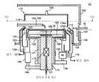
이어서, 도 2 내지 도 4를 참조하여 이 실시예의 반도체 제조 장치에서의 무전해 도금 유닛(11)에 대하여 상세하게 설명한다. 도 2에 도시한 바와 같이, 무전해 도금 유닛(11)(이하, 「도금 유닛(11)」이라고도 함)은, 외부 챔버(110), 내부 챔버(120), 스핀 척(130), 제 1?제 2 유체 공급부(140?150), 가스 공급부(160), 백플레이트(165)를 구비하고 있다.Next, the
외부 챔버(110)는, 하우징(100)의 안에 배설되어 도금 처리를 실행하는 처리 용기이다. 외부 챔버(110)는, 기판(W)의 수납 위치를 둘러싸는 통 형상으로 형성되고, 하우징(100)의 저면에 고정되어 있다. 외부 챔버(110)의 측면에는 기판(W)을 반출입하는 윈도우(115)가 설치되어 셔터 기구(116)에 의하여 개폐 가능하게 되어 있다. 또한, 외부 챔버(110)의 윈도우(115)가 형성된 측과 대향하는 측면에는, 제 1?제 2 유체 공급부(140?150)의 동작을 위한 셔터 기구(119)가 개폐 가능하게 형성되어 있다. 외부 챔버(110)의 상면에는 가스 공급부(160)가 설치되어 있다. 외부 챔버(110)의 하부에는, 가스 또는 처리액 등을 배출하는 드레인 배출기(118)가 구비되어 있다.The
내부 챔버(120)는, 기판(W)으로부터 비산하는 처리액을 받는 용기이며, 외부 챔버(110)의 안에 배설되어 있다. 내부 챔버(120)는 외부 챔버(110)와 기판(W)의 수납 위치의 사이의 위치에 통 형상으로 형성되고, 배기, 배액용의 드레인 배출 기(124)를 구비하고 있다. 내부 챔버(120)는, 예를 들면 가스 실린더 등의 도시하지 않은 승강 기구를 이용하여, 외부 챔버(110)의 내측에서 승강이 가능하게 되어 있고, 상단부(122)의 단부가 기판(W)의 수납 위치보다 조금 높은 위치(처리 위치)와, 해당 처리 위치보다 하방의 위치(퇴피 위치)의 사이에서 승강한다. 여기서 처리 위치란, 기판(W)에 무전해 도금을 실시할 때의 위치이며, 퇴피 위치란, 기판(W)의 반출입시 또는 기판(W)의 세정 등을 행할 때의 위치이다.The
스핀 척(130)은, 기판(W)을 실질적으로 수평하게 유지하는 기판 고정 기구이다. 스핀 척(130)은, 회전 통체(131), 회전 통체(131)의 상단부로부터 수평으로 넓어지는 고리 형상의 회전 플레이트(132), 회전 플레이트(132)의 외주단에 원주 방향으로 등간격을 두고 설치된 기판(W)의 외주부를 지지하는 지지 핀(134a), 마찬가지로 기판(W)의 외주면을 압압하는 복수의 압압 핀(134b)을 가지고 있다. 도 3에 도시한 바와 같이, 지지 핀(134a)과 압압 핀(134b)은, 서로 원주 방향으로 이격되어, 예를 들면 3 개씩 배치되어 있다. 지지 핀(134a)은, 기판(W)을 유지하여 소정의 수용 위치에 고정되는 고정구이며, 압압 핀(134b)은, 기판(W)을 하방으로 압압하는 압압 기구이다. 회전 통체(131)의 측방에는 모터(135)가 설치되어 있고, 모터(135)의 구동축과 회전 통체(131)의 사이에는 무단(無端) 형상의 벨트(136)가 감겨져 있다. 즉, 모터(135)에 의해 회전 통체(131)가 회전하도록 구성된다. 지지 핀(134a) 및 압압 핀(134b)은 수평 방향(기판(W)의 면 방향)으로 회전하고, 이들에 의해 유지되는 기판(W)도 수평 방향으로 회전한다.The
가스 공급부(160)는, 외부 챔버(110)의 안으로 질소 가스 또는 클린 에어를 공급하여 기판(W)을 건조시킨다. 공급된 질소 가스 또는 클린 에어는, 외부 챔버(110)의 하단에 설치된 드레인 배출기(118 또는 124)를 통해 회수된다.The
백플레이트(165)는, 스핀 척(130)이 유지한 기판(W)의 하면에 대향하고, 스핀 척(130)에 의한 기판(W)의 유지 위치와 회전 플레이트(132)의 사이에 배설되어 있다. 백플레이트(165)는, 히터를 내장하고 있으며, 회전 통체(131)의 축심을 관통하는 샤프트(170)와 연결되어 있다. 백플레이트(165)의 안에는, 그 표면의 복수 개소에서 개구하는 유로(166)가 형성되어 있고, 이 유로(166)와 샤프트(170)의 축심을 관통하는 유체 공급로(171)가 연통하고 있다. 유체 공급로(171)에는 열 교환기(175)가 배치되어 있다. 열 교환기(175)는, 순수 또는 건조 가스 등의 처리 유체를 소정의 온도로 조정한다. 즉, 백플레이트(165)는, 온도 조정된 처리 유체를 기판(W)의 하면을 향하여 공급하는 작용을 한다. 샤프트(170)의 하단부에는 연결 부재(180)를 통하여 에어 실린더 등의 승강 기구(185)가 연결되어 있다. 즉, 백플레이트(165)는, 승강 기구(185) 및 샤프트(170)에 의하여, 스핀 척(130)에서 유지된 기판(W)과 회전 플레이트(132)의 사이를 승강하도록 구성되어 있다.The
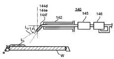
도 3에 도시한 바와 같이, 제 1?제 2 유체 공급부(140?150)는, 스핀 척(130)에 의하여 유지된 기판(W)의 상면에 처리액을 공급한다. 제 1?제 2 유체 공급부(140?150)는, 처리액 등의 유체를 저장하는 유체 공급 장치(200)와, 공급용 노즐을 구동하는 노즐 구동 장치(205)를 구비하고 있다. 제 1?제 2 유체 공급부(140?150)는, 하우징(100)의 안에서 외부 챔버(110)를 개재할 수 있도록 각각 배치되어 있다.As shown in FIG. 3, the first to second
제 1 유체 공급부(140)는, 유체 공급 장치(200)와 접속된 제 1 배관(141)과, 제 1 배관(141)을 지지하는 제 1 암(142)과, 제 1 암(142)의 기부(基部)에 구비되어 스테핑 모터 등을 이용하여 해당 기부를 축으로, 제 1 암(142)을 선회시키는 제 1 선회 구동 기구(143)를 구비하고 있다. 제 1 유체 공급부(140)는, 무전해 도금 처리액 등의 처리 유체를 공급하는 기능을 가진다. 제 1 배관(141)은, 3 종의 유체를 개별적으로 공급하는 배관(141a?141b?141c)을 포함하고, 각각 제 1 암(142)의 선단부에서 노즐(144a?144b?144c)과 접속되어 있다.The first
마찬가지로, 제 2 유체 공급부(150)는, 유체 공급 장치(200)와 접속된 제 2 배관(151)과, 제 2 배관(151)을 지지하는 제 2 암(152)과, 제 2 암(152)의 기부(基部)에 구비되어 제 2 암(152)을 선회시키는 제 2 선회 구동 기구(153)를 구비하고 있다. 제 2 배관(151)은, 제 2 암(152)의 선단부에서 노즐(154)과 접속되어 있다. 제 2 유체 공급부(150)는, 기판(W)의 외주부(주연부)의 처리를 행하는 처리 유체를 공급하는 기능을 가진다. 제 1 및 제 2 암(142 및 152)은, 외부 챔버(110)에 설치된 셔터 기구(119)를 통해 스핀 척(130)에 유지된 기판(W)의 상방을 선회한다.Similarly, the second
여기서, 도 4를 참조하여 유체 공급 장치(200)에 대하여 상세하게 설명한다. 유체 공급 장치(200)는, 제 1?제 2 유체 공급부(140?150)에 처리 유체를 공급한다. 도 4에 도시한 바와 같이, 유체 공급 장치(200)는, 제 1 탱크(210), 제 2 탱크(220), 제 3 탱크(230), 및 제 4 탱크(240)를 가지고 있다.Here, with reference to FIG. 4, the
제 1 탱크(210)는 기판(W)의 무전해 도금 처리의 전처리에 사용되는 전세정 처리액(L1)을 저장한다. 또한, 제 2 탱크(220)는 기판(W)의 무전해 도금 처리의 후처리에 사용되는 후세정 처리액(L2)을 저장한다. 제 1 및 제 2 탱크(210 및 220)는, 각각 처리액(L1?L2)을 소정의 온도로 조정하는 온도 조절 기구(도시하지 않음)를 구비하고 있고, 제 1 배관(141a)과 접속된 배관(211) 및 제 1 배관(141b)과 접속된 배관(221)이 접속되어 있다. 배관(211 및 221)에는, 각각 펌프(212 및 222)와, 밸브(213 및 223)가 구비되어 있고, 소정 온도로 조절된 처리액(L1?L2)이, 각각 제 1 배관(141a)?제 1 배관(141b)으로 공급되도록 구성되어 있다. 즉, 펌프(212 및 222)와 밸브(213 및 223)를 각각 작동시킴으로써, 처리액(L1?L2)이 제 1 배관(141a) 및 제 1 배관(141b)을 통하여 노즐(144a) 및 노즐(144b)로 송출된다.The
제 3 탱크(230)는, 기판(W)을 처리하는 도금액(L3)을 저장한다. 제 3 탱크(230)는, 제 1 배관(141c)과 접속된 배관(231)이 접속되어 있다. 배관(231)에는, 펌프(232), 밸브(233), 및 도금액(L3)을 가열하는 가열기(예를 들면, 열 교환기)(234)가 설치되어 있다. 즉, 도금액(L3)은, 가열기(234)에 의하여 온도 조절되고, 펌프(232) 및 밸브(233)의 협동 동작에 의하여 제 1 배관(141c)을 통하여 노즐(144c)로 송출된다.The
제 4 탱크(240)는, 기판(W)의 외주부의 처리에 이용되는 외주부 처리액(L4)을 저장한다. 제 4 탱크(240)는, 제 2 배관(151)과 접속된 배관(241)이 접속되어 있다. 배관(241)에는, 펌프(242) 및 밸브(243)가 설치되어 있다. 즉, 외주부 처리액(L4)은, 펌프(242) 및 밸브(243)의 협동 동작에 의해 제 2 배관(151)을 통하여 노즐(154)로 송출된다.The
또한, 제 4 탱크(240)에는, 예를 들면 불산을 공급하는 배관, 과산화수소수를 공급하는 배관 및 순수(L0)를 공급하는 배관 등도 접속되어 있다. 즉, 제 4 탱크(240)는, 이들 액을 사전에 설정된 소정의 비율로 혼합하여 조정하는 작용도 하게된다.The
또한, 제 1 배관(141a) 및 제 1 배관(141b)에는, 각각 순수(L0)를 공급하는 배관(265a 및 265b)이 접속되고, 배관(265a)에는 밸브(260a)가 설치되고, 배관(265b)에는 밸브(260b)가 설치되어 있다. 즉, 노즐(144a 및 144b)은 순수(L0)도 공급할 수 있다.Further,
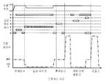
이어서, 도 1 내지 도 7를 참조하여, 이 실시예에서의 도금 유닛(11)의 동작을 설명한다. 도 5는, 이 실시예에 따른 도금 유닛(11)의 동작을 나타낸 순서도, 도 6은, 이 실시예에 따른 도금 유닛(11)의 프로세스의 흐름을 나타낸 도면, 도 7은, 마찬가지로 도금액 처리의 프로세스의 흐름을 나타낸 도면이다. 도 5에 도시한 바와 같이, 이 실시예의 도금 유닛(11)은, 전세정 공정(도 중 「A」), 도금 처리 공정(도 중 「B」), 후세정 공정(도 중 「C」), 이면?단면 세정 공정(도 중 「D」), 및 건조 공정(도 중 「E」)의 5 개의 공정을 실현한다. 또한, 도 6에 도시한 바와 같이, 이 실시예의 도금 유닛(11)은, 기판 이면에 가온된 순수를 공급하는 이 면 순수 공급(a), 기판 단면을 세정하는 단면 세정(b), 기판 이면을 세정하는 이면 세정(c), 도금 처리에 이어서 기판을 세정하는 후세정(d), 도금 처리(e), 도금 처리에 앞서 기판을 세정하는 전세정(f), 및 기판의 친수도를 조정하는 순수 공급(g)의 7 개의 처리액 공급 프로세스를 실행한다.1 to 7, the operation of the
제 1 기판 반송 기구(9)는, 반출입부(1)의 후프(F)로부터 기판(W)을 1 매씩 반출하여, 처리부(2)의 전달 유닛(10)으로 기판(W)을 반입한다. 기판(W)이 반입되면, 제 2 기판 반송 기구(14)는 기판(W)을 가열 유닛(12) 및 냉각 유닛(13)으로 반송하고, 기판(W)은 소정의 열처리가 행해진다. 열처리가 종료되면, 제 2 기판 반송 기구(14)는, 무전해 도금 유닛(11) 내로 기판(W)을 반입한다.The 1st board |
제 2 기판 반송 기구(14)의 반송 암(14A)은, 윈도우(115)를 통해 기판(W)을 스핀 척(130)으로 전달한다. 스핀 척(130)은, 기판(W)을 지지 핀(134a) 및 압압 핀(134b)에 의하여 유지한다. 기판(W)이 반송되면, 셔터 기구(116)가 폐쇄되어 외부 챔버(110)는 처리 대기 상태가 된다.The
우선, 프로세스 컨트롤러(51)는, 전세정 공정(A)을 실행한다. 전세정 공정(A)은, 친수화 처리, 전세정 처리, 순수 처리를 포함하고 있다.First, the
프로세스 컨트롤러(51)는, 모터(135)를 구동하여 스핀 척(130)에 유지된 기판(W)을 회전시킨다(단계 300. 이하, 「S300」이라고 함). 스핀 척(130)은, 예를 들면 100 ~ 500 rpm 정도, 바람직하게는 250 rpm 정도로 회전시킨다.The
스핀 척(130)이 회전하면, 프로세스 컨트롤러(51)는, 노즐 구동 장치(205)에 제 1 유체 공급부(140)의 구동을 지시한다. 노즐 구동 장치(205)는, 제 1 선회 구 동 기구(143)를 작동시켜서 제 1 암(142)을 기판(W) 상의 소정 위치(예를 들면 노즐(144a)이 기판(W)의 중심부가 되는 위치)로 이동시킨다(S301). 또한, 노즐 구동 장치(205)는, 제 2 선회 구동 기구(153)를 작동시켜서 제 2 암(152)을 기판(W) 상의 주연부로 이동시킨다. 각각 소정 위치에 도달하면, 프로세스 컨트롤러(51)는, 유체 공급 장치(200)에 친수화 처리를 지시한다. 유체 공급 장치(200)는, 밸브(260a)를 열어서 소정량의 순수(L0)를 노즐(144a)로 보낸다(도 6 중 공급 프로세스(g)). 이 때, 노즐(144a)은, 예를 들면 기판(W)의 상방 0.1 ~ 20 mm 정도의 위치로 해 둔다(S302). 마찬가지로, 유체 공급 장치(200)는, 밸브(243)를 열어서 처리액(L4)을 노즐(154)로 보낸다. 이 처리에서의 처리액(L4)은, 순수(L0)와의 관계에서 상이한 친수화 효과가 얻어지는 것을 이용한다.When the
이 친수화 처리는, 이어서 전세정액이 기판(W) 표면에서 튀기는 것을 방지하고, 또한, 도금액이 기판(W) 표면으로부터 쉽게 떨어지지 않게하는 작용을 한다. 순수(L0)의 공급 속도는, 기판(W)의 표면의 소수성에 따라 조정되고, 0.5 ~ 2.0 [L / 분]으로 하는 것이 효과적이다. 특히, 소수성이 강한 절연막(예를 들면 SiOCH 등의 유기계의 저유전율막)에서는, 1.5 [L / 분] 정도로 하는 것이 보다 바람직하다. 기판(W)의 회전 속도는, 예를 들면 1000 rpm 이상의 회전수에서는 제대로 친수화를 도모할 수 없으므로, 예를 들면 100 ~ 500 rpm의 회전수로 하는 것이 효과적이다. 이 친수화 처리의 처리 시간은 기판(W)의 종류에 따라 적절히 설정되고, 예를 들면 5 ~ 30 초 동안 정도로 할 수 있다. 제 1 유체 공급부(140)와 제 2 유체 공급부(150)는, 협동적으로 기판(W)의 중심부 부근 및 주연부 부근 각각의 친수도를 조정하여, 기판(W) 전체에서 균일한 도금 처리가 행해지도록 한다. 노즐(144a) 및 노즐(154) 각각의 위치는, 도금 처리의 조건 등에 따라 변경할 수 있고, 기판(W)의 중심부 및 주연부 각각의 친수도의 대소도 임의로 변경할 수 있다.This hydrophilization treatment then prevents the pre-cleaning liquid from splashing on the surface of the substrate W, and also serves to prevent the plating liquid from easily falling off the surface of the substrate W. FIG. The supply rate of the pure water L0 is adjusted according to the hydrophobicity of the surface of the substrate W, and it is effective to set it to 0.5 to 2.0 [L / min]. In particular, an insulating film having a high hydrophobicity (for example, an organic low dielectric constant film such as SiOCH) is more preferably about 1.5 [L / min]. Since the rotation speed of the board | substrate W cannot hydrophilize suitably at the rotation speed of 1000 rpm or more, for example, it is effective to set it as the rotation speed of 100-500 rpm, for example. The processing time of this hydrophilization treatment is appropriately set according to the type of the substrate W, and can be, for example, about 5 to 30 seconds. The first
도 8a 및 도 8b는, 이러한 친수화 처리의 상태를 나타내고 있다. 도 8a는, 제 1 유체 공급부(140) 및 제 2 유체 공급부(150)를 측면에서 본 개념도, 도 8b는, 제 1 유체 공급부(140)가 순수(L0)를 공급하고, 제 2 유체 공급부(150)가 처리액(L4)을 공급하여 친수화 처리를 행하는 상태를 나타낸 도면이다. 도 8a 및 도 8b에 도시한 바와 같이, 제 1 암(142)은 기판(W)의 대략 중앙부, 제 2 암(152)은 기판(W)의 주연부에 배치되고, 순수(L0)가 노즐(144a)로부터, 처리액(L4)이 노즐(154)로부터 기판(W) 표면으로 공급된다. 여기서, 도 8a에 도시한 바와 같이, 제 1 유체 공급부(140) 및 제 2 유체 공급부(150)는, 순수(L0)와 처리액(L4) 등의 온도를 조절하는 온도 조절기(145?155)와, 순수(L0)와 처리액(L4) 등을 노즐(144a?154)로 송출하는 펌프 기구(146?156)를 가지고 있어도 좋다. 펌프 기구(146?156)는, 순수(L0) 및 처리액(L4) 등을 노즐(144a, 154)로 송출할 뿐만 아니라, 반대로, 노즐(144a, 154)로부터 순수(L0) 및 처리액(L4)을 흡입하는 기능도 가지고 있다. 즉, 펌프 기구(146?156)는, 소정량의 순수(L0) 등이 공급된 후, 노즐(144a?154)의 선 단으로부터 순수(L0)?처리액(L4) 등이 떨어지지 않도록, 남은 순수(L0)?처리액(L4) 등을 재흡입하는 작용을 한다. 이 구성을 구비함으로써, 기판(W) 상에 발생하는 유체의 불균일을 방지할 수 있다.8A and 8B show the state of such hydrophilization treatment. FIG. 8A is a conceptual view of the first
이어서, 프로세스 컨트롤러(51)는, 유체 공급 장치(200)에 전세정 처리(도 6 중 공급 프로세스(f)) 및 이면 온순수 공급(도 6 중 공급 프로세스(a))을 지시한다. 유체 공급 장치(200)는, 밸브(260a)를 닫아 순수(L0)의 공급을 멈추고, 또한, 밸브(243)를 닫아 처리액(L4)의 공급을 멈추고, 펌프(212) 및 밸브(213)를 구동시켜 전세정 처리액(L1)을 노즐(144a)로 공급한다(S303). 여기서, 노즐(144a)은 기판(W)의 대략 중앙부로 이동한 상태이므로, 노즐(144a)은, 기판(W)의 대략 중앙부로 전세정 처리액(L1)을 공급하게 된다. 전세정 처리액은 유기산 등을 이용하므로, 갈바닉 부식(galvanic corrosion)을 발생시키지 않고, 구리 배선 상으로부터 산화 구리를 제거하여, 도금 처리 시의 핵 형성 밀도를 상승시킬 수 있다. 전세정 처리액(L1)의 공급 속도는, 기판(W)의 표면에 부착된 순수(L0)를 치환할 필요가 있으므로, 0.5 ~ 2.0 [L / 분]으로 하는 것이 바람직하다. 기판(W)의 회전 속도에 대해서는, 너무 느리면 제거해야 할 금속종을 기판(W)의 표면으로부터 제거할 수 없다. 한편, 기판(W)의 회전 속도가 너무 빠르면 기판(W)의 표면에 건조되는 개소가 발생되므로, 구리 배선의 표면이 산화될 우려가 있다. 이 때문에, 예를 들면 100 ~ 500 rpm 정도의 회전 속도로 하는 것이 바람직하다. 전세정 처리의 처리 시간은, 너무 길게 하면 구리 영역을 과도하게 용해하게 되므로, 예를 들면 10 ~ 60 초 정도가 바람직하다.Subsequently, the
이어서, 유체 공급 장치(200)는, 유체 공급로(171)에 순수를 공급한다. 열 교환기(175)는, 유체 공급로(171)로 보내지는 순수를 온도 조절하고, 백플레이트(165)에 설치된 유로(166)을 통해 온도 조절된 순수를 기판(W)의 하면으로 공급한다(S304). 이에 의해, 기판(W)의 온도가 도금 처리에 적합한 온도로 유지된다. 또한, 유체 공급로(171)로의 순수의 공급은, 상술한 단계 S300와 동시에 개시해도 동일한 효과를 얻을 수 있다.Next, the
전세정 처리가 종료되면, 프로세스 컨트롤러(51)는, 유체 공급 장치(200)로 순수 처리(도 6 중 공급 프로세스(g))를 지시한다(S305). 유체 공급 장치(200)는, 펌프(212) 및 밸브(213)를 작동시켜 전세정 처리액(L1)의 공급을 멈추고, 또한, 밸브(260a)를 열어서 소정량의 순수(L0)를 노즐(144a)로 보낸다. 노즐(144a)로부터의 순수(L0)의 공급에 의해, 전세정 처리액을 순수로 치환하게 된다. 이는, 산성인 전세정 처리액(L1)과 알칼리성인 도금 처리액이 혼합하여 프로세스 불량이 발생하는 것을 방지하는 것이다. 이 순수 처리는, 기판(W) 상의 구리 배선이 산화하지 않도록 기판(W)을 건조시키지 않게 연속적으로 실행하는 것이 바람직하다. 순수 처리는, 순수 공급량을 0.5 ~ 2.0 [L / 분], 기판(W)의 회전 속도를 100 ~ 500 rpm, 처리 시간을 10 ~ 60 초 정도로 하는 것이 바람직하다.When the pre-cleaning process is completed, the
전세정 공정(A)에 이어서, 프로세스 컨트롤러(51)는, 도금 처리 공정(B)을 실행한다. 도금 처리 공정(B)은, 도금액 치환 처리, 도금액 축적 처리, 도금액 처리, 순수 처리를 포함하고 있다. 도 7에서, X로 나타낸 처리가 도금액 치환 처리, Y로 나타낸 처리가 도금액 축적 처리, Z로 나타낸 처리가 도금액 처리에 대응한다.Following the pre-cleaning step (A), the
프로세스 컨트롤러(51)는, 유체 공급 장치(200) 및 노즐 구동 장치(205)에 도금액 치환 처리를 지시한다(도 6 중 공급 프로세스(e)). 유체 공급 장치(200)는, 밸브(260a)를 닫아 순수(L0)의 공급을 멈추고(S310), 또한, 펌프(232)와 밸브(233)를 작동시켜 도금액(L3)을 노즐(144c)로 공급한다(S311). 한편, 노즐 구동 장치(205)는, 제 1 선회 구동 기구(143)를 작동시켜, 노즐(144c)이 기판(W)의 중앙부 ~ 주연부 ~ 중앙부로 이동(스캔)하도록 제 1 암(142)을 선회시킨다(S312). 즉, 도 7에 도시한 바와 같이, 도금액 치환 처리(X)에서는, 도금액 공급 노즐이 중앙부 ~ 주연부 ~ 중앙부를 이동하고, 기판(W)이 비교적 높은 회전수로 회전한다. 이 동작에 의해, 도금액(L3)이 기판(W) 상을 확산하여, 기판(W)의 표면 상의 순수를 신속하게 도금액으로 치환할 수 있다. 여기서, 기판(W)의 회전수는 100 ~ 300 rpm 정도, 제 1 암(142)의 선회 속도는, 노즐(144c)이 150 [mm / 초] 정도로 이동하는 속도로 하는 것이 바람직하다. 이 때, 노즐(144c)이 중앙부로부터 주연부로 이동하는 속도와 주연부로부터 중앙부로 이동하는 속도가 상이해도 좋다. 이 처리는, 기판(W) 상의 순수가 남는 것을 해소할 수 있다. 특히, 제 1 암(142)의 선회(노즐(144c)의 이동)와 도금액(L3)의 공급을 동시에 행함으로써, 기판(W) 상의 도금 액(L3)의 온도 저하를 방지하고, 또한, 기판(W) 전체의 온도 상승 효율을 높이는 것을 가능하게 한다.The
도금액 치환 처리가 종료되면, 프로세스 컨트롤러(51)는, 스핀 척(130)에 유지된 기판(W)의 회전 속도를 감속시키고(S313), 유체 공급 장치(200) 및 노즐 구동 장치(205)에 도금액 축적 처리를 지시한다. 이 시점에서의 기판(W)의 회전 속도는, 50 ~ 100 rpm 정도가 바람직하다. 유체 공급 장치(200)는 계속해서 도금액(L3)을 공급하고, 노즐 구동 장치(205)는 제 1 선회 구동 기구(143)를 작동시키고, 노즐(144c)이 기판(W)의 중앙부로부터 주연부를 향해 서서히 이동시킨다(S314). 도금액 치환 처리된 기판(W)의 표면은, 충분한 양의 도금액(L3)이 축적된다. 즉, 도 7에 도시한 바와 같이, 도금액 축적 처리에서는, 노즐이 중앙으로부터 주연부를 향해 이동하면서 도금액이 연속 공급된다. 이에 따라, 기판(W) 전역에서 균일한 도금 처리가 실현된다.When the plating liquid replacement process is completed, the
또한, 노즐(144c)이 기판(W)의 주연부 근방에 가까워진 단계에서, 프로세스 컨트롤러(51)는 기판(W)의 회전 속도를 더욱 감속시킨다(S315). 이 단계(예를 들어 1 ~ 2 초 동안 정도)에서는, 기판(W)의 회전 속도는, 통상의 도금 처리와 동등한 5 ~ 20 rpm 정도로 하는 것이 바람직하다. 도금 처리를 안정적으로 행하기 위해서이다.In addition, when the
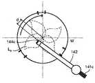
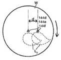
이어서, 프로세스 컨트롤러(51)는, 유체 공급 장치(200) 및 노즐 구동 장치(205)에 도금 처리를 지시한다. 노즐 구동 장치(205)는, 제 1 선회 구동 기 구(143)를 작동시켜, 노즐(144c)이 기판(W)의 중앙부와 주연부의 대략 중간 위치에 위치하도록 제 1 암(142)을 선회시킨다(S316). 노즐(144c)의 위치는, 예를 들어 기판(W)의 중심으로부터 30 ~ 100 mm 정도, 보다 바람직하게는 30 ~ 70 mm 정도, 반경 방향으로 이탈시킨 장소로 하는 것이 바람직하다. 도 9는, 이러한 노즐(144c)의 상태를 나타내고 있다. 도 9는, 제 1 유체 공급부(140)를 상면에서 본 개념도이다. 도 9에 도시한 바와 같이, 제 1 암(142)은, 노즐(144c)이 기판(W)의 중앙부와 주연부의 중간(기판(W)의 중앙으로부터 거리 d 이간한 위치)으로 이동하여, 도금액(L3)이 기판(W) 상으로 간헐적으로 공급된다. 이러한 구성 및 동작에 의해, 도금액이 기판(W)의 전체면으로 골고루 펼쳐진다.Subsequently, the
이어서, 유체 공급 장치(200)는, 펌프(232)와 밸브(233)를 동작시켜 도금액(L3)을 노즐(144c)에 단속(斷續)적?간헐적으로 공급한다(S317). 즉, 도 7에 도시한 바와 같이, 노즐이 소정 위치에 배치되어 도금액이 단속적?간헐적으로 공급된다. 기판(W)은 회전하고 있으므로, 도금(L3)을 단속적(간헐적)으로 공급해도 기판(W)의 전역에 골고루 도금액(L3)을 퍼지게 할 수 있다. 또한, 상기 단계 311 내지 317의 처리는, 반복적으로 행해도 좋다. 도금액(L3)을 공급하고 소정 시간 경과 후, 유체 공급 장치(200)는, 도금액(L3)의 공급을 정지하고, 프로세스 컨트롤러(51)는, 기판(W)의 이면으로의 온순수의 공급을 정지한다(S318). 도금액의 공급량은 기판(W)의 표면에 공급되는 도금액이 마르지 않을 정도이면 되고, 예를 들면 100 ~ 400 [mL / 분] 정도로 하면 된다. 또한, 기판(W)의 회전수는, 가열 불균일 또는 원심력에 의한 건조를 방지하기 위해, 1 ~ 25 rpm 정도로 하는 것이 바람직하다. 도금액(L3)의 공급 시간은, 생성되는 도금막의 두께에 따라 적절히 결정할 수 있다. 도금액 공급의 간헐의 정도(공급 온오프의 비율)는, 공급되는 기간(온)이 길어도 되고, 공급되지 않는 기간(오프)이 길어도 좋다.Next, the
또한, 프로세스 컨트롤러(51)는, 유체 공급 장치(200) 및 노즐 구동 장치(205)에 순수 처리를 지시한다(도 6 중 공급 프로세스(g)). 프로세스 컨트롤러(51)는, 스핀 척(130)에 유지된 기판(W)의 회전 속도를 증속시키고(S319), 노즐 구동 장치(205)는, 제 1 선회 구동 기구(143)를 동작시켜 노즐(144c)이 기판(W)의 중앙부에 위치하도록 제 1 암(142)을 선회시킨다(S320). 그 후, 유체 공급 장치(200)는, 밸브(260a)를 열어서 순수(L0)를 공급한다(S321). 이에 따라, 기판(W) 표면에 남은 도금액을 제거하여 후처리액과 도금액이 섞이는 것을 방지할 수 있다. 이 처리는, 구리 배선이 산화하지 않도록 기판(W)을 건조시키지 않는 상태에서 행할 필요가 있다. 순수의 공급량으로서는, 예를 들면 0.5 ~ 2.0 [L / 분]으로 하는 것이 바람직하고, 기판(W)의 회전수는, 예를 들면 100 ~ 500 rpm 정도가 바람직하다. 또, 처리 시간은, 도금액이 기판(W)의 표면으로부터 제거될 수 있으면 되고, 예를 들면 10 ~ 60 초 정도로 할 수 있다.In addition, the
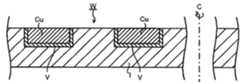
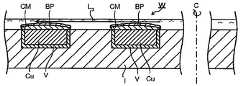
도 10a 내지 도 10d는, 기판(W) 표면의 도금 처리의 상태를 나타낸 도면이다. 도 10a에 도시한 바와 같이, 기판(W)에는, 그 표면에 절연막(I)과, 절연막(I) 의 표층부에 형성된 배리어 메탈(V)과, 배리어 메탈(V)을 통해 절연막(I)의 표층에 형성된 구리(Cu) 배선이 형성되어 있다. 이 실시예의 도금 유닛(11)에서는, 기판(W)을 회전시킴과 동시에, 노즐(144c)을 기판(W)의 중앙부와 주연부의 대략 중간의 위치로 하여 도금액을 공급하므로, 원심력에 의하여 도금액(L3)이 기판(W)의 표면을 흐르도록 공급된다(도 10b). 도금 처리가 진행되면, 구리(Cu) 배선의 표면에 캡 메탈(CM)이 형성된다. 아울러, 기판(W)의 표면에 반응 부생성물(BP)이 생성된다(도 10c). 또한, 이 도금액(L3)의 흐름에 의하여, 기판(W)의 표면에서의 도금 반응에 의한 반응 부생성물(BP)을 포함하는 오래된 도금액(L3)이 기판(W)의 외측으로 연속적으로 배출된다. 이 때문에, 기판(W) 표면에 반응 부생성물(BP)을 머무르게 하지 않고 항상 새로운 도금액(L3)으로 캡 메탈(도금 처리막)을 성장시킬 수 있다(도 10d).10A to 10D are diagrams showing a state of plating treatment on the surface of the substrate W. FIG. As shown in FIG. 10A, the substrate W has an insulating film I formed on its surface, a barrier metal V formed on the surface layer portion of the insulating film I, and a barrier metal V formed thereon. Copper (Cu) wiring formed in the surface layer is formed. In the
도금 처리 공정(B)에 이어서, 프로세스 컨트롤러(51)는 후세정 공정(C)을 실행한다. 후세정 공정(C)은, 후약액 처리 및 순수 처리를 포함하고 있다.Following the plating treatment step (B), the
프로세스 컨트롤러(51)는, 유체 공급 장치(200)에 후약액 처리를 지시한다(도 6 중 공급 프로세스(d)). 유체 공급 장치(200)는, 밸브(260a)를 닫아 순수(L0)의 공급을 정지시키고, 또한, 펌프(222) 및 밸브(223)를 동작시켜 후세정 처리액(L2)을 노즐(144b)로 공급한다(S330). 후세정 처리액(L2)은, 기판(W)의 표면의 잔사물 또는 이상 석출한 도금막을 제거하는 작용을 한다. 후세정 처리액(L2)의 공급 량은, 표면이 마르지 않는 정도의 양이면 되므로, 예를 들면 0.5 ~ 2.0 [L / 분] 정도의 양으로 할 수 있다. 또한, 기판(W)의 회전수는, 기판(W)의 표면을 건조시키지 않고, 또한 후세정 처리액(L2)이 기판(W)의 표면에 충분히 퍼질 필요가 있으므로, 예를 들면 100 ~ 500 rpm 정도로 하는 것이 바람직하다.The
후약액 처리에 이어서, 프로세스 컨트롤러(51)는, 유체 공급 장치(200)에 순수 처리를 지시한다(도 6 중 공급 프로세스(g)). 유체 공급 장치(200)는, 펌프(222) 및 밸브(223)를 작동시켜 후세정 처리액(L2)의 공급을 정지시키고, 또한, 밸브(260b)를 열어서 순수(L0)를 공급한다(S331). 순수의 공급량으로서는, 예를 들면 0.5 ~ 2.0 [L / 분]으로 하는 것이 바람직하고, 기판(W)의 회전수는, 예를 들면 100 ~ 500 rpm 정도가 바람직하다. 또한, 처리 시간은, 도금액이 기판(W)의 표면으로부터 제거될 수 있으면 되고, 예를 들면 10 ~ 60 초 정도로 할 수 있다.Subsequently to the chemical liquid treatment, the
후세정 공정(C)에 이어서, 프로세스 컨트롤러(51)는, 이면?단면 세정 공정(D)을 실행한다. 이면?단면 세정 공정(D)은, 액 제거 처리, 이면 세정 처리, 단면(端面) 세정 처리를 포함하고 있다.Following the post-cleaning step (C), the
프로세스 컨트롤러(51)는, 유체 공급 장치(200)에 액 제거 처리를 지시한다. 유체 공급 장치(200)는, 밸브(260b)를 닫아 순수(L0)의 공급을 정지하고, 프로세스 컨트롤러(51)는, 스핀 척(130)에 유지된 기판(W)의 회전 속도를 증속한다(S340). 이 처리는, 기판(W)의 이면을 건조시켜서 기판(W)의 표면의 액 제거를 목적으로 하고 있다. 기판(W)의 회전 속도는, 예를 들면 800 ~ 1000 rpm 정도로 고속 회전된 다. 처리 시간은, 기판(W)의 표면이 친수성을 가지므로, 10 ~ 30 초 정도로 하는 것이 바람직하다.The
액 제거 처리가 종료되면, 프로세스 컨트롤러(51)는, 유체 공급 장치(200)에 이면 세정 처리를 지시한다. 우선, 프로세스 컨트롤러(51)는, 우선, 스핀 척(130)에 유지된 기판(W)의 회전 속도를 감속시킨다(S341). 이 때의 회전 속도는, 처리액의 되튀김 방지를 위해, 예를 들면 5 ~ 20 rpm 정도의 비교적 낮은 속도로 한다. 이어서, 유체 공급 장치(200)는, 유체 공급로(171)에 순수를 공급한다(도 6 중 공급 프로세스(a)). 열 교환기(175)는, 유체 공급로(171)로 보내지는 순수를 온도 조절하고, 백플레이트(165)에 설치된 유로를 통해 온도 조절된 순수를 기판(W)의 이면으로 공급한다(S342). 순수는, 기판(W)의 이면측을 친수화하는 작용을 한다. 이어서, 유체 공급 장치(200)는, 유체 공급로(171)로의 순수 공급을 정지시키고, 대신에 이면 세정액을 유체 공급로(171)에 공급한다(S343). 이면 세정액은, 도금 처리에서의 기판(W)의 이면측의 잔사물을 세정 제거하는 작용을 한다(도 6 중 공급 공정(c)).When the liquid removal process is completed, the
그 후, 프로세스 컨트롤러(51)는, 유체 공급 장치(200) 및 노즐 구동 장치(205)에 단면 세정 처리를 지시한다. 유체 공급 장치(200)는, 기판(W)의 이면에 이면 세정액의 공급을 정지하고, 대신에 열 교환기(175)에 의하여 온도 조절된 순수를 유체 공급로(171)에 공급한다(S344). 이 때, 기판(W)의 회전수를 비교적 낮은 5 ~ 20 rpm으로 해두고, 되튀김을 방지하는 것이 바람직하다(도 6 중 공급 프로세스(a)).Thereafter, the
이어서, 노즐 구동 장치(205)는, 제 2 선회 구동 기구(153)를 작동시켜 노즐(154)이 기판(W)의 단부(端部)에 위치하도록 제 2 암(152)을 선회시키고, 프로세스 컨트롤러(51)는, 기판(W)의 회전수를 150 ~ 300 rpm 정도로 증속시킨다(S345). 마찬가지로, 노즐 구동 장치(205)는, 제 1 선회 구동 기구(143)를 작동시켜 노즐(144b)이 기판(W)의 중앙부에 위치하도록 제 1 암(142)을 선회시킨다. 유체 공급 장치(200)는, 밸브(260b)를 열어 순수(L0)를 노즐(144b)에 공급하고, 또한, 펌프(242) 및 노즐(243)을 작동시켜 외주부 처리액(L4)을 노즐(154)로 공급한다(도 6 중 공급 프로세스(a?g)). 즉, 이 상태에서는, 기판(W)의 중앙부에 순수(L0), 마찬가지로 단부에 외주부 처리액(L4)이 공급되고, 기판(W)의 이면에 온도 조절된 순수가 공급되게 된다(S346).Subsequently, the
도 11a 및 도 11b는, 이러한 단면 세정 처리의 상태를 도시하고 있다. 도 11a는, 제 1?제 2 유체 공급부(140?150)를 상면에서 본 개념도, 도 11b는, 제 1?제 2 유체 공급부(140?150)가 순수(L0) 및 외주부 처리액(L4)을 공급하여 단면 세정 처리를 행하는 상태를 도시한 도면이다. 도 11a 및 도 11b에 도시한 바와 같이, 제 1 암(142)은 노즐(144b)이 기판(W) 중앙부에 위치하도록 이동하고, 제 2 암(152)은 노즐(154)이 기판(W)의 주연부에 위치하도록 이동한다. 그리고, 순수(L0) 및 외주부 처리액(L4)이 노즐(144b) 및 노즐(154)로부터 기판(W) 표면에 각각 공급된다. 이러한 구성 및 동작에 의하여, 기판(W)의 표면 및 단면에 남은 잔사물을 제 거하는 것이 가능해진다. 이 단면 세정 처리에서의 외주부 처리액(L4)으로서는, 예를 들어 불산 등을 이용할 수 있다.11A and 11B show the state of this end face cleaning process. 11A is a conceptual view of the first to second
이면?단면 세정 공정(D)에 이어서, 프로세스 컨트롤러(51)는, 건조 공정(E)을 실행한다. 건조 공정(E)은 건조 처리를 포함하고 있다.Subsequently, the
프로세스 컨트롤러(51)는, 유체 공급 장치(200) 및 노즐 구동 장치(205)에 건조 처리를 지시한다. 유체 공급 장치(200)는, 모든 처리액 공급을 정지시키고(S350), 노즐 구동 장치(205)는, 제 1 암(142) 및 제 2 암(152)을 기판(W)의 상방으로부터 퇴피시킨다. 또한, 프로세스 컨트롤러(51)는, 기판(W)의 회전 속도를 800 ~ 1000 rpm 정도까지 증속하여 기판(W)을 건조시킨다(S351). 건조를 위한 시간은, 예를 들면 10 ~ 30 초 정도가 바람직하다. 건조 처리가 종료되면, 프로세스 컨트롤러(51)는 기판(W)의 회전을 정지시킨다(S352).The
도금 처리 공정이 종료되면, 제 2 기판 반송 기구(14)의 반송 암(14A)은, 윈도우(115)를 통해 기판(W)을 스핀 척(130)으로부터 취출한다.When the plating treatment step is completed, the
이 실시예의 도금액 유닛(11)에 의하면, 도금 처리 공정(B)에서, 도금액 치환 처리에 의하여 도금액 공급 노즐을, 기판(W) 상을 이동시키면서 도금액을 공급했으므로, 도금액의 온도 저하를 방지하면서 기판(W) 상의 액 불균일을 억제할 수 있다. 또한, 이 실시예의 도금액 유닛(11)에 의하면, 도금액 노즐을 기판(W)의 중앙부와 단부의 사이의 위치로 하여 도금액을 단속 공급(간헐 공급)하였으므로, 도금액 공급량을 억제하면서 기판(W)의 표면에 골고루 도금액을 공급할 수 있다.According to the plating
여기서, 이 실시예의 반도체 제조 장치에서의 노즐(144)의 변형예에 대하여 설명한다. 도 12a 및 도 12b는, 이 실시예의 제 1 유체 공급부(140)의 변형예를 도시한 도면, 도 12c는, 제 1 유체 공급부(140)의 변형예에 의한 도금 처리의 상태를 도시한 도면이다. 도 12a에 도시한 바와 같이, 이 변형예에서는, 제 1 유체 공급부(140)의 노즐(144a/144b/144c)이, 기판(W)의 피처리면의 방향으로부터 노즐 경사각(θ)의 방향을 향한 노즐(144d/144e/144f)로 치환되어 있다. 이 변형예에 의하면, 도금액(L3) 등을 공급하는 노즐을 기판(W)의 처리면에 대해 소정의 노즐 경사각(θ)으로 경사지게 하였으므로, 도금액(L3)의 튐을 억제하고, 또한, 기판(W) 상에 보다 균일하게 도금액(L3)을 공급할 수 있다.Here, a modification of the nozzle 144 in the semiconductor manufacturing apparatus of this embodiment will be described. 12A and 12B show a modification of the first
또한, 제 1 유체 공급부(140)의 노즐(144a/144b/144c)(또는, 노즐(144d/144e/144f))은, 기판(W)의 중심일 필요는 없다. 이 실시예의 반도체 제조 장치에서는, 기판(W)을 회전시키면서 도금액을 기판(W) 상으로 공급한다. 이 때문에, 사용하는 도금액의 절약 또는 도금액 공급에 따른 액의 튐을 억제하는 관점에서, 도 12b에 도시한 바와 같이, 노즐(144)을 기판 중심으로부터 주연부 방향으로 거리 d만큼 이간시키는 것도 가능하다. 즉, 도 12c에 도시한 바와 같이, 기판(W)의 회전과의 상승(相乘) 효과에 의해, 도금액을 기판(W) 상에 보다 골고루 공급하는 것을 기대할 수 있다.In addition, the
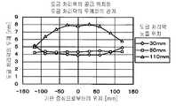
이어서, 도 13 내지 도 15를 참조하여, 이 실시예에 따른 도금액 유닛(11)의 동작예를 설명한다. 도 13은, 상술한 도금 처리 공정(B)에서의 도금 처리액의 토출 간격과 도금 처리막의 두께의 관계를 나타낸 도면, 도 14는, 마찬가지로 노즐(144c)의 노즐 경사각과 도금 처리막의 두께의 관계를 나타낸 도면, 도 15는, 마찬가지로 노즐(144c)에 의한 도금액의 토출 위치와 도금 처리막의 두께의 관계를 나타낸 도면이다.Next, with reference to FIGS. 13-15, the operation example of the plating
도 13에 나타낸 예에서는, 기판(W)으로서 300 mm 반도체 웨이퍼를 이용하고, 노즐(144c)의 경사각을 60 도로 설정했다. 이 때, 노즐(144c)의 위치는 기판(W) 상방에서 기판(W) 중앙부와 주연부의 대략 중간 위치로 했다. 이 상태에서 도금 처리 공정(B)의 도금 처리를 실행하여, 기판(W) 상의 도금 처리막의 두께를 계측했다. 비교를 위해, 노즐(144c)로부터의 도금액(L3)의 토출 간격(공급 간격)을, 도금액 공급 1에 대해 비공급 9(1:9), 마찬가지로 공급 3에 대해 비공급 7(3:7), 마찬가지로 공급 10에 대해 비공급 없음(10:0, 연속 공급)으로 했다.In the example shown in FIG. 13, the inclination angle of the
그 결과, 도 13에 도시한 바와 같이, 도금액의 토출 간격과 도금 처리막의 막 두께의 상관은 인정되지 않았다. 이는, 도금액을 연속 공급하지 않고 간헐 공급했어도 막 두께의 균일성에 문제가 없다는 것을 의미하고 있다. 즉, 도금액을 간헐 공급함으로써, 도금액 공급량을 절약하는 것이 가능해진다.As a result, as shown in Fig. 13, the correlation between the discharge interval of the plating liquid and the film thickness of the plating film was not recognized. This means that even if the plating liquid is intermittently supplied without being continuously supplied, there is no problem in the uniformity of the film thickness. That is, by supplying a plating liquid intermittently, it becomes possible to save the plating liquid supply amount.
또, 도 14에 나타낸 예에서는, 기판(W)으로서 300 mm의 반도체 웨이퍼를 이용하여, 노즐(144c)의 위치를 기판(W) 상방에서 기판(W) 중앙부와 주연부의 대략 중간 위치로 한 채로, 노즐(144c)의 노즐 경사각을 45 도, 60 도, 90 도로 한 3 개의 경우에 대하여, 노즐 경사각과 도금 처리막의 두께와의 관계를 조사했다. 여기 서, 경사각이란, 도 10a에 도시한 바와 같이, 기판(W) 처리면을 기준으로 한 노즐의 경사각(θ)이다.In addition, in the example shown in FIG. 14, using the 300-mm semiconductor wafer as the board | substrate W, the position of the
그 결과, 경사각 90 도 및 45 도인 경우에서 기판(W) 주연부의 막 두께가 두꺼워지는 경향이 인정되었다. 특히, 경사각 90 도(기판(W)에 대해 수직으로 도금액을 공급)인 경우, 기판(W)의 중심으로부터 50 mm까지는 균일한 막 두께가 얻어졌으나, 50 mm를 초과하여 주연부가 되면 막 두께가 급격하게 두꺼워지는 결과가 되었다. 이는, 기판(W) 외주부의 액 축적 효과에 의해 도금액이 기판(W) 상으로부터 원활히 배출되지 않고, 반응 부생성물이 외주부에 쌓인 결과, 해당 부분의 막 두께가 두꺼워진 것이라고 생각된다. 따라서, 노즐 경사각은 기판(W) 처리면에 대해, 어느 일정한 범위의 각도를 가지는 것이 바람직하다. 또한, 경사각 45 도인 경우, 노즐(144c)로부터 공급되는 도금액이 기판(W) 상에서 충분히 확산되지 않아, 기판(W) 외주부의 일부의 막 두께가 두꺼워진 것이라고 생각된다. 이들 경향으로부터, 노즐(144c)의 경사각은 기판에 대해 45 도 이상, 보다 바람직하게는 60 도 전후(오차를 ± 10 도로 하면 50 ~ 70 도 정도)로 하는 것이 바람직하다.As a result, the tendency for the film thickness of the periphery of the board | substrate W to become thick in the case of inclination angle 90 degree and 45 degree was recognized. Particularly, in the case of an inclination angle of 90 degrees (supplying the plating liquid perpendicularly to the substrate W), a uniform film thickness was obtained from the center of the substrate W to 50 mm, but when the peripheral portion exceeded 50 mm, the film thickness was increased. The result is a sharp thickening. This is considered to be because the plating liquid is not discharged smoothly from the substrate W due to the liquid accumulation effect on the outer peripheral portion of the substrate W, and as a result of the reaction by-products accumulating on the outer peripheral portion, the film thickness of the portion becomes thick. Therefore, it is preferable that the nozzle inclination angle has a certain range of angles with respect to the substrate W processing surface. In addition, when the inclination angle is 45 degrees, the plating liquid supplied from the
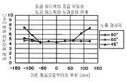
또한, 도 15에 나타낸 예에서는, 기판(W)으로서 300 mm의 반도체 웨이퍼를 이용하여, 노즐(144c)의 경사각을 45 도로 하고, 노즐(144c)의 위치를 기판(W) 중심으로부터 30 mm, 50 mm, 110 mm의 3 개의 경우에 대해, 노즐의 위치와 도금 처리막의 두께와의 관계를 조사하였다. 도금 처리액의 공급 위치, 즉, 노즐의 위치는, 도 12c에 도시한 기판(W)의 중심으로부터의 거리 d의 위치이다. 도금액의 분사는 기판(W)의 회전에 따른 방향으로 행하였다.In the example illustrated in FIG. 15, the inclination angle of the
그 결과, 노즐(144c)의 도금액 토출 위치를 기판(W) 중심으로부터 110 mm 이간한 위치로 한 경우에, 기판(W) 중앙부와 주연부의 사이에서 도금 처리막의 막 두께에 큰 차이(중앙부의 쪽이 막 두께가 두꺼움)가 인정되었다. 이는, 기판(W) 주연부에서의 액 축적 처리의 효과가 저해되어, 기판(W) 내주부로 퍼진 도금액이 건조되었으므로, 내주부의 도금액이 중첩 도포되어 막 두께가 두꺼워진 것으로 생각된다. 또한, 노즐(144c)의 도금액 토출 위치를 기판(W)의 중심으로부터 30 mm 이간한 위치로 한 경우에, 작지만 기판(W) 중앙부와 주연부의 사이에서 막 두께에 차이(주연부의 쪽이 막 두께가 두꺼움)가 인정되었다. 한편, 노즐(144c)의 도금액 토출 위치를 기판(W) 중심으로부터 50 mm 이간한 위치로 한 경우, 대체로 균일한 막 두께를 얻을 수 있었다. 이 점에서, 도금 처리를 행할 때의 노즐(144c)의 위치는, 기판(W) 상의 중앙부에 과도하게 근접하거나, 또는 주연부에 과도하게 근접하면 균일성이 저해되므로, 양자의 대략 중간점으로 하는 것이 바람직하다는 것을 알 수 있다. 구체적으로는, 거리 d가 30 ~ 110 mm, 보다 바람직하게는 거리 d가 50 mm정도(오차 ± 20 mm로서 30 ~ 70 mm 정도)로 하는 것이 바람직하다.As a result, in the case where the plating liquid discharge position of the
여기서 설명한 노즐 경사각은, 기판(W)에 공급되어 실제로 반응에 기여하는 도금액의 온도의 유지와, 기판(W)에 공급되는 도금액의 신선도에 영향을 준다. 도금 처리 프로세스에서는, 도금액이 노즐로부터 공급되어 기판(W)의 표면에 도달하여 반응할 때에 소정의 조건의 온도로 되는 것이 바람직하고, 이 온도를 유지하는 것이 큰 과제가 된다. 이 실시예에서의 노즐의 경사는, 기판(W) 상에 도금액을 체류시키는 것을 방지하므로, 기판(W)의 표면에서의 도금액 온도를 적절한 온도로 유 지하는 것이 가능해진다. 또, 기판(W)의 표면 상에 도금액이 체류되는 것을 억제함으로써, 기판(W) 상에서 반응에 기여를 마친 오래된 도금액이 쌓여있는 것을 방지하고, 항상 새로운 도금액이 기판(W) 상에서 도금 처리에 기여하는 것이 가능해진다.The nozzle inclination angle described here affects the maintenance of the temperature of the plating liquid supplied to the substrate W and actually contributed to the reaction, and the freshness of the plating liquid supplied to the substrate W. In the plating treatment process, when the plating liquid is supplied from the nozzle to reach the surface of the substrate W and reacts, it is preferable that the plating liquid be at a temperature of a predetermined condition, and maintaining this temperature is a major problem. Since the inclination of the nozzle in this embodiment prevents the plating liquid from staying on the substrate W, it is possible to maintain the plating liquid temperature on the surface of the substrate W at an appropriate temperature. In addition, by suppressing the plating liquid from remaining on the surface of the substrate W, the old plating liquid which has contributed to the reaction on the substrate W is prevented from being accumulated, and a new plating liquid always contributes to the plating treatment on the substrate W. It becomes possible.
마찬가지로, 도금액 공급의 간헐 비율에 대해서도, 기판(W)에 공급되어 실제로 반응에 기여하는 도금액의 온도의 유지와, 기판(W)에 공급되는 도금액의 신선도에 영향을 준다. 노즐 경사각의 도금 처리 프로세스에 대한 작용과 마찬가지로, 도금액을 연속 공급하는 경우에 비해, 간헐 공급으로 함으로써 기판(W)의 표면 상에 도금액이 체류되는 것을 방지할 수 있게 되고, 도금액 온도의 유지와 도금액의 리프레쉬에 효과를 기대할 수 있다.Similarly, the intermittent ratio of the plating liquid supply also affects the maintenance of the temperature of the plating liquid supplied to the substrate W and actually contributed to the reaction, and the freshness of the plating liquid supplied to the substrate W. Similarly to the operation of the plating process of the nozzle inclination angle, compared with the case of continuously supplying the plating liquid, the intermittent supply makes it possible to prevent the plating liquid from remaining on the surface of the substrate W, and to maintain the plating liquid temperature and the plating liquid. The effect can be expected to refresh.
이어서, 도 16a 내지 도 16c를 참조하여, 본 발명의 다른 실시예에 따른 반도체 제조 장치에 대하여 설명한다. 도 16a는, 이 실시예에 따른 반도체 제조 장치의 무전해 도금 유닛의 단면도, 도 16b 및 도 16c는, 이 실시예에 따른 무전해 도금 유닛에 의한 도금 처리의 상태를 도시한 도면이다. 이 실시예에 따른 반도체 제조 장치는, 도 1 내지 도 3에 도시한 실시예에 따른 반도체 제조 장치와 동일한 구성을 가지고 있고, 도금액(L3)이 제 1 유체 공급부(140)가 아니라, 샤프트(170)에 설치된 유체 공급로(171)를 통하여 공급되는 점이 상이하다. 여기서, 도 1 내지 도 3에 도시한 실시예와 공통되는 구성에 대하여 동일한 부호를 붙여서 나타내고, 중복되는 설명을 생략한다. 이 실시예는, 기판(W)의 하면에 도금 처리를 실시하는, 이른바 페이스 다운 방식을 적용한 예이다.Next, a semiconductor manufacturing apparatus according to another embodiment of the present invention will be described with reference to FIGS. 16A to 16C. 16A is a cross-sectional view of the electroless plating unit of the semiconductor manufacturing apparatus according to this embodiment, and FIGS. 16B and 16C are views showing the state of plating treatment by the electroless plating unit according to this embodiment. The semiconductor manufacturing apparatus according to this embodiment has the same configuration as the semiconductor manufacturing apparatus according to the embodiments shown in FIGS. 1 to 3, and the plating liquid L3 is not the first
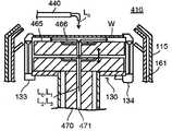
도 16a에 도시한 바와 같이, 이 실시예의 무전해 도금 유닛(410)은, 제 1 유체 공급부(440)와, 백플레이트(465)를 구비하고 있다. 제 1 유체 공급부(440)는, 스핀 척(130)에 의해 유지된 기판(W)의 상면에 처리액 또는 순수 등을 공급한다. 백플레이트(465)는, 스핀 척(130)이 유지하는 기판(W)의 하면에 대향하고, 스핀 척(130)에 의한 기판(W)의 유지 위치와 회전 플레이트(132)의 사이에 배설되어 있다. 이 실시예에서는, 스핀 척(130)은, 기판(W)의 피처리면을 백플레이트(465)에 대향시켜 기판(W)을 유지한다.As shown in FIG. 16A, the
백플레이트(465)의 안에는, 그 표면의 복수 개소에서 개구하는 유로(466)가 형성되어 있고, 이 유로(466)와 샤프트(470)의 축심을 관통하는 유체 공급로(471)가 연통하고 있다. 유체 공급로(471)에는 도시하지 않은 열 교환기가 배치되어 있고, 도금액 등의 처리 유체를 소정의 온도로 조정한다. 즉, 백플레이트(165)는, 온도 조정된 처리 유체를 기판(W)의 하면을 향하여 공급하는 작용을 한다. 도금 처리시에, 유체 공급 장치(200)는, 전처리액(L1), 후처리액(L2), 도금액(L3)을 유체 공급로(471)를 통해 기판(W)의 피처리면(하면)으로 공급한다. 한편, 기판(W)의 온도를 조절하는 순수(L0)는, 제 1 유체 공급부(440)에 의하여 기판(W)의 상면에 공급된다.In the
이 실시예에서의 도금 처리 공정에서는, 유체 공급로(471)가 순수(L0), 전세정 처리액(L1), 후세정 처리액(L2), 도금액(L3)을 기판(W)의 하면으로 공급하고, 제 1 유체 공급부(440)가 온도 조절된 순수(L0)를 기판(W)의 상면으로 공급하는 점을 제외하고, 도 5에 나타낸 제 1 실시예의 공정과 거의 공통된다. 즉, 도금 처리의 대상이 기판(W)의 하면인 점만 상이하다. 백플레이트(465)는, 전세정 처리액(L1), 후세정 처리액(L2), 도금액(L3)을 기판(W)의 하면으로 공급할 때에 상승하여 기판(W)과 접근한 상태로 한다. 즉, 이들 처리 유체는, 기판(W)과 백플레이트(465)의 사이의 간극을 기판(W)의 주연부를 향하여 흐르게 된다. 이 실시예의 반도체 제조 장치에 의하면, 도금액 등의 처리액을 기판(W)에 접근시킨 백플레이트(465)와 기판(W)과의 사이를 흐르게함으로써 기판(W)을 처리하므로, 도금액 등의 사용량을 절약할 수 있다.In the plating treatment step in this embodiment, the
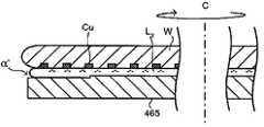
여기서, 이 실시예의 무전해 도금 유닛(410)의 백플레이트(465)에 대하여 상세하게 설명한다. 도 16b 및 도 16c에 도시한 바와 같이, 이 실시예의 백플레이트(465)는, 그 표면의 도금액 등 처리 유체에 대한 젖음성이 중앙부와 주연부에서 상이하도록 설계되어 있다. 즉, 백플레이트(465)의 주연부(α)는, 중앙부(β)보다 처리 유체에 대한 젖음성이 낮아지도록 구성되어 있다.Here, the
일반적으로, 백플레이트(465)와 같은 플레이트의 표면의 처리 유체에 대한젖음성이 낮은 경우는, 해당 플레이트 표면 상에서의 처리 유체의 표면 장력이 강하게 작용하는 경향이 있고, 젖음성이 높을 경우는, 처리 유체가 해당 플레이트 표면을 퍼지게 흐르기 쉬워지는 성질이 있음이 알려져 있다. 이 실시예의 백플레이트(465)에서는, 플레이트의 주연부에 대하여 처리 유체에 대한 젖음성을 중앙부보 다 낮게 하였으므로, 플레이트 주연부에서는, 처리 유체의 표면 장력에 의하여 처리 유체가 플레이트 중앙부를 향하여 갇히는 방향으로 힘이 작용한다. 또한, 플레이트 중앙부에서는 플레이트 표면 상을 확산하는 방향으로 힘이 작용한다. 즉, 도 16b 및 도 16c에 도시한 화살표의 방향으로 힘이 작용하므로, 처리 유체가 백플레이(465)의 면 내에서 골고루 퍼져, 기판(W)의 표면 전면을 균일하게 적시는 것이 가능해진다. 이에 따라, 기판(W) 상의 도금 처리를 보다 균일하게 할 수 있다.In general, when the wettability of the surface of the plate, such as the
또한, 본 발명은 상기 실시예 그대로 한정되지 않고, 실시 단계에서는 그 요지를 일탈하지 않는 범위에서 구성 요소를 변형하여 구체화할 수 있다. 또한, 상기 실시예에 개시되어 있는 복수의 구성 요소의 적절한 조합에 의해, 다양한 발명을 형성할 수 있다. 예를 들면, 실시예에 도시된 전체 구성 요소로부터 몇 개의 구성 요소를 삭제해도 좋다. 또한, 상이한 실시예에 걸친 구성 요소를 적절히 조합해도 좋다.In addition, this invention is not limited to the said Example as it is, In an implementation step, it can embody by changing a component in the range which does not deviate from the summary. Moreover, various inventions can be formed by appropriate combination of the some component disclosed by the said Example. For example, some components may be deleted from all the components shown in the embodiments. Moreover, you may combine suitably the components over different embodiments.
예를 들어, 백플레이트 표면의 젖음성을 중심부와 주연부에서 상이한 것으로 하는 수단으로서, 백플레이트에 단차를 두어 백플레이트 표면이 처리 유체에 주는 힘을 조절할 수도 있다. 도 17a 및 도 17b는, 이러한 백플레이트의 예를 도시한 도면이다. 도 17a 및 도 17b에 도시한 바와 같이, 단차 α'또는 단차 β'를 백플레이트 표면에 설치하고, 백플레이트 표면의 중심부 및 주연부 각각의 처리 유체에 대한 저항, 즉, 젖음성을 조절해도 좋다.For example, as a means of making the wettability of the backplate surface different at the center and the periphery, the backplate may be stepped to regulate the force exerted on the processing fluid by the backplate surface. 17A and 17B show an example of such a back plate. As shown in Figs. 17A and 17B, the step α 'or step β' may be provided on the back plate surface, and the resistance, i.e., the wettability, to the treatment fluid of each of the center and the periphery of the back plate surface may be adjusted.
마찬가지로, 도 16b 및 도 16c에 도시한 백플레이트 표면의 젖음성을 중심부와 주연부에서 상이한 것으로 하는 기술적 사상은, 도 1 내지 도 3에 도시한 실시 예에도 적용할 수 있다. 상술한 바와 같이, 전세정 공정(A)에서, 제 1 유체 공급부(140)의 노즐(144a)을 기판(W)의 중앙으로 이동시키고, 제 2 유체 공급부(150)의 노즐(154)를 기판(W)의 주연부로 이동시켜, 각각 순수(L0)와 외주부 처리액(L4)을 공급한다. 이 때, 외주부 처리액(L4)을 적절히 조정함으로써, 기판(W)의 중앙부와 주연부에서 젖음성을 상이한 것으로 할 수 있게 된다. 이러한 처리에 의해, 전세정 공정(A)에 이어지는 도금 처리 공정(B)에서, 도금액이 기판(W) 상에 균일하게 쌓이게 할 수 있다.Similarly, the technical idea that the wettability of the surface of the back plate shown in FIGS. 16B and 16C is different at the center and the periphery may be applied to the embodiments shown in FIGS. 1 to 3. As described above, in the pre-cleaning step (A), the
본 발명은, 반도체 제조업에 적용할 수 있다.The present invention can be applied to a semiconductor manufacturing industry.
도 1은 본 발명에 따른 일실시예의 반도체 제조 장치의 구성을 도시한 평면도이다.1 is a plan view showing the configuration of a semiconductor manufacturing apparatus of one embodiment according to the present invention.
도 2는 이 실시예의 반도체 제조 장치에서의 무전해 도금 유닛을 도시한 단면도이다.2 is a cross-sectional view showing an electroless plating unit in the semiconductor manufacturing apparatus of this embodiment.
도 3은 이 실시예의 반도체 제조 장치에서의 무전해 도금 유닛을 도시한 평면도이다.3 is a plan view showing an electroless plating unit in the semiconductor manufacturing apparatus of this embodiment.
도 4는 이 실시예의 반도체 장치에서의 유체 공급 장치의 구성을 도시한 도면이다.4 is a diagram showing the configuration of a fluid supply device in the semiconductor device of this embodiment.
도 5는 이 실시예의 도금 유닛의 동작을 나타낸 순서도이다.5 is a flowchart showing the operation of the plating unit of this embodiment.
도 6은 이 실시예에 따른 도금 유닛의 공정의 흐름을 나타낸 도면이다.6 is a view showing a flow of a process of a plating unit according to this embodiment.
도 7은 이 실시예에 따른 도금 유닛의 도금액 처리의 프로세스의 흐름을 나타낸 도면이다.7 is a view showing a flow of a process of plating liquid treatment of a plating unit according to this embodiment.
도 8a는 제 1 유체 공급부를 측면에서 본 개념도이다.8A is a conceptual view of the first fluid supply viewed from the side.
도 8b는 제 1 유체 공급부가 순수를 공급하여 친수화 처리를 행하는 상태를 도시한 도면이다.8B is a view showing a state in which the first fluid supply unit supplies pure water to perform a hydrophilization treatment.
도 9는 제 1 유체 공급부를 상면에서 본 개념도이다.9 is a conceptual view of the first fluid supply unit viewed from above.
도 10a는 기판 표면의 도금 처리의 상태를 도시한 도면이다.It is a figure which shows the state of the plating process of the board | substrate surface.
도 10b는 기판 표면의 도금 처리의 상태를 도시한 도면이다.It is a figure which shows the state of the plating process of the board | substrate surface.
도 10c는 기판 표면의 도금 처리의 상태를 도시한 도면이다.It is a figure which shows the state of the plating process of the board | substrate surface.
도 10d는 기판 표면의 도금 처리의 상태를 도시한 도면이다.It is a figure which shows the state of the plating process of the substrate surface.
도 11a는 제 1?제 2 유체 공급부를 상면에서 본 개념도이다.11A is a conceptual view of a first fluid supply part viewed from an upper surface thereof.
도 11b는 제 1?제 2 유체 공급부를 측면에서 본 개념도이다.11B is a conceptual view of the first fluid supply part and the second fluid supply device.
도 12a는 제 1 유체 공급부의 변형예를 도시한 도면이다.12A is a view showing a modification of the first fluid supply part.
도 12b는 제 1 유체 공급부의 변형예를 도시한 도면이다.12B is a view showing a modification of the first fluid supply part.
도 12c는 제 1 유체 공급부의 변형예에 의한 도금 처리의 상태를 도시한 도면이다.It is a figure which shows the state of the plating process by the modification of a 1st fluid supply part.
도 13은 도금 처리 공정에서의 도금 처리액의 토출 간격과 도금 처리막의 두께의 관계를 나타낸 도면이다.It is a figure which shows the relationship between the discharge interval of the plating process liquid and the thickness of a plating process film in a plating process.
도 14는 노즐의 경사각과 도금 처리막의 두께의 관계를 나타낸 도면이다.14 is a diagram showing a relationship between the inclination angle of the nozzle and the thickness of the plating film.
도 15는 노즐에 의한 도금액의 토출 위치와 도금 처리막의 두께의 관계를 나타낸 도면이다.15 is a diagram showing a relationship between the discharge position of the plating liquid by the nozzle and the thickness of the plating film.
도 16a는 다른 실시예의 반도체 장치의 무전해 도금 유닛의 구성을 도시한 단면도이다.16A is a cross-sectional view illustrating a configuration of an electroless plating unit of a semiconductor device of another embodiment.
도 16b은 이 실시예의 무전해 도금 유닛에 의한 도금 처리의 상태를 도시한 도면이다.Fig. 16B is a diagram showing the state of plating treatment by the electroless plating unit of this embodiment.
도 16c는 이 실시예의 무전해 도금 유닛에 의한 도금 처리의 상태를 도시한 도면이다.FIG. 16C is a diagram showing a state of plating treatment by the electroless plating unit of this embodiment.
도 17a은 이 실시예의 무전해 도금 유닛에서의 백플레이트의 변형예를 도시한 도면이다.17A is a view showing a modification of the back plate in the electroless plating unit of this embodiment.
도 17b는 이 실시예의 무전해 도금 유닛에서의 백플레이트의 변형예를 도시한 도면이다.17B is a view showing a modification of the back plate in the electroless plating unit of this embodiment.
* 도면의 주요 부분에 대한 부호의 설명 *Explanation of symbols on the main parts of the drawings
1 : 반출입부1: Import / Export
2 : 처리부2: processing unit
3 : 반송부3: conveying part
5 : 제어 장치5: control device
11 : 무전해 도금 유닛11: electroless plating unit
51 : 프로세스 컨트롤러51: process controller
110 : 외부 챔버110: outer chamber
120 : 내부 챔버120: inner chamber
130 : 스핀 척130: spin chuck
132 : 회전 플레이트132: rotating plate
134a : 지지 핀134a: support pin
134b : 압압 핀134b: pressing pin
140 : 제 1 유체 공급부140: first fluid supply
142 : 제 1 암142: first arm
143 : 제 1 선회 구동 기구143: first turning drive mechanism
144a?144b?144c : 노즐144a? 144b? 144c: Nozzle
150 : 제 2 유체 공급부150: second fluid supply portion
152 : 제 2 암152: second arm
153 : 제 2 선회 구동 기구153: second swing drive mechanism
154 : 노즐154: nozzle
160 : 가스 공급부160: gas supply unit
165 : 백플레이트165: backplate
166 : 유로166: Euro
170 : 샤프트170: shaft
171 : 유체 공급로171: fluid supply passage
175 : 열 교환기175: heat exchanger
200 : 유체 공급 장치200: fluid supply device
205 : 노즐 구동 장치205: nozzle driving device
Claims (22)
Translated fromKoreanPriority Applications (1)
| Application Number | Priority Date | Filing Date | Title |
|---|---|---|---|
| KR1020090023061AKR101123705B1 (en) | 2008-04-04 | 2009-03-18 | Semiconductor manufacturing apparatus and semiconductor manufacturing method |
Applications Claiming Priority (2)
| Application Number | Priority Date | Filing Date | Title |
|---|---|---|---|
| JPJP-P-2008-098367 | 2008-04-04 | ||
| KR1020090023061AKR101123705B1 (en) | 2008-04-04 | 2009-03-18 | Semiconductor manufacturing apparatus and semiconductor manufacturing method |
Publications (2)
| Publication Number | Publication Date |
|---|---|
| KR20090106339A KR20090106339A (en) | 2009-10-08 |
| KR101123705B1true KR101123705B1 (en) | 2012-03-15 |
Family
ID=41535960
Family Applications (1)
| Application Number | Title | Priority Date | Filing Date |
|---|---|---|---|
| KR1020090023061AActiveKR101123705B1 (en) | 2008-04-04 | 2009-03-18 | Semiconductor manufacturing apparatus and semiconductor manufacturing method |
Country Status (1)
| Country | Link |
|---|---|
| KR (1) | KR101123705B1 (en) |
Cited By (2)
| Publication number | Priority date | Publication date | Assignee | Title |
|---|---|---|---|---|
| KR20150024795A (en)* | 2013-08-27 | 2015-03-09 | 도쿄엘렉트론가부시키가이샤 | Substrate processing method, substrate processing apparatus and storage medium |
| US10835908B2 (en) | 2013-08-27 | 2020-11-17 | Tokyo Electron Limited | Substrate processing method |
Families Citing this family (3)
| Publication number | Priority date | Publication date | Assignee | Title |
|---|---|---|---|---|
| KR101147305B1 (en)* | 2010-10-12 | 2012-05-18 | 나노씨엠에스(주) | Silver thin-film spread apparatus by means of deposition of nano metallic silver |
| JP5788349B2 (en)* | 2012-03-19 | 2015-09-30 | 東京エレクトロン株式会社 | Plating processing apparatus, plating processing method, and storage medium |
| US11352711B2 (en) | 2019-07-16 | 2022-06-07 | Applied Materials, Inc. | Fluid recovery in semiconductor processing |
Citations (2)
| Publication number | Priority date | Publication date | Assignee | Title |
|---|---|---|---|---|
| JP2005029820A (en)* | 2003-07-09 | 2005-02-03 | Toshiba Corp | Plating method, semiconductor device manufacturing method, and plating apparatus |
| KR20070058310A (en)* | 2005-12-02 | 2007-06-08 | 도쿄 엘렉트론 가부시키가이샤 | Electroless Plating Apparatus and Electroless Plating Method |
- 2009
- 2009-03-18KRKR1020090023061Apatent/KR101123705B1/enactiveActive
Patent Citations (2)
| Publication number | Priority date | Publication date | Assignee | Title |
|---|---|---|---|---|
| JP2005029820A (en)* | 2003-07-09 | 2005-02-03 | Toshiba Corp | Plating method, semiconductor device manufacturing method, and plating apparatus |
| KR20070058310A (en)* | 2005-12-02 | 2007-06-08 | 도쿄 엘렉트론 가부시키가이샤 | Electroless Plating Apparatus and Electroless Plating Method |
Cited By (3)
| Publication number | Priority date | Publication date | Assignee | Title |
|---|---|---|---|---|
| KR20150024795A (en)* | 2013-08-27 | 2015-03-09 | 도쿄엘렉트론가부시키가이샤 | Substrate processing method, substrate processing apparatus and storage medium |
| US10835908B2 (en) | 2013-08-27 | 2020-11-17 | Tokyo Electron Limited | Substrate processing method |
| KR102233590B1 (en)* | 2013-08-27 | 2021-03-30 | 도쿄엘렉트론가부시키가이샤 | Substrate processing method, substrate processing apparatus and storage medium |
Also Published As
| Publication number | Publication date |
|---|---|
| KR20090106339A (en) | 2009-10-08 |
Similar Documents
| Publication | Publication Date | Title |
|---|---|---|
| JP4547016B2 (en) | Semiconductor manufacturing apparatus and semiconductor manufacturing method | |
| KR101123704B1 (en) | Cap metal forming method | |
| KR100958557B1 (en) | Substrate processing method and substrate processing apparatus | |
| KR101123705B1 (en) | Semiconductor manufacturing apparatus and semiconductor manufacturing method | |
| KR101178868B1 (en) | Supply apparatus, semiconductor manufacturing apparatus, and semiconductor manufacturing method | |
| WO2013080778A1 (en) | Plating apparatus, plating method and storage medium | |
| JP3485561B1 (en) | Electroless plating method and electroless plating apparatus | |
| JP5631815B2 (en) | Plating treatment method, plating treatment apparatus, and storage medium | |
| KR101123703B1 (en) | Cap metal forming method | |
| JP5095786B2 (en) | Semiconductor manufacturing method | |
| JP5331096B2 (en) | Plating equipment | |
| TW202036758A (en) | Substrate liquid processing apparatus and substrate liquid processing method | |
| TW202133297A (en) | Substrate liquid processing method and substrate liquid processing device | |
| WO2013080779A1 (en) | Plating apparatus, plating method and storage medium | |
| KR20140031329A (en) | Plating processing device, plating processing method, and recording medium | |
| TW202106925A (en) | Substrate processing method and substrate processing apparatus |
Legal Events
| Date | Code | Title | Description |
|---|---|---|---|
| A201 | Request for examination | ||
| PA0109 | Patent application | Patent event code:PA01091R01D Comment text:Patent Application Patent event date:20090318 | |
| PA0201 | Request for examination | ||
| PG1501 | Laying open of application | ||
| E902 | Notification of reason for refusal | ||
| PE0902 | Notice of grounds for rejection | Comment text:Notification of reason for refusal Patent event date:20110314 Patent event code:PE09021S01D | |
| E701 | Decision to grant or registration of patent right | ||
| PE0701 | Decision of registration | Patent event code:PE07011S01D Comment text:Decision to Grant Registration Patent event date:20111130 | |
| GRNT | Written decision to grant | ||
| PR0701 | Registration of establishment | Comment text:Registration of Establishment Patent event date:20120228 Patent event code:PR07011E01D | |
| PR1002 | Payment of registration fee | Payment date:20120229 End annual number:3 Start annual number:1 | |
| PG1601 | Publication of registration | ||
| FPAY | Annual fee payment | Payment date:20150130 Year of fee payment:4 | |
| PR1001 | Payment of annual fee | Payment date:20150130 Start annual number:4 End annual number:4 | |
| FPAY | Annual fee payment | Payment date:20160127 Year of fee payment:5 | |
| PR1001 | Payment of annual fee | Payment date:20160127 Start annual number:5 End annual number:5 | |
| FPAY | Annual fee payment | Payment date:20170202 Year of fee payment:6 | |
| PR1001 | Payment of annual fee | Payment date:20170202 Start annual number:6 End annual number:6 | |
| FPAY | Annual fee payment | Payment date:20180219 Year of fee payment:7 | |
| PR1001 | Payment of annual fee | Payment date:20180219 Start annual number:7 End annual number:7 | |
| FPAY | Annual fee payment | Payment date:20190218 Year of fee payment:8 | |
| PR1001 | Payment of annual fee | Payment date:20190218 Start annual number:8 End annual number:8 | |
| FPAY | Annual fee payment | Payment date:20200218 Year of fee payment:9 | |
| PR1001 | Payment of annual fee | Payment date:20200218 Start annual number:9 End annual number:9 | |
| PR1001 | Payment of annual fee | Payment date:20210218 Start annual number:10 End annual number:10 | |
| PR1001 | Payment of annual fee | Payment date:20230131 Start annual number:12 End annual number:12 | |
| PR1001 | Payment of annual fee | Payment date:20240119 Start annual number:13 End annual number:13 | |
| PR1001 | Payment of annual fee | Payment date:20250108 Start annual number:14 End annual number:14 |