KR101123542B1 - Single-layer touch-sensitive display - Google Patents
Single-layer touch-sensitive displayDownload PDFInfo
- Publication number
- KR101123542B1 KR101123542B1KR1020107009798AKR20107009798AKR101123542B1KR 101123542 B1KR101123542 B1KR 101123542B1KR 1020107009798 AKR1020107009798 AKR 1020107009798AKR 20107009798 AKR20107009798 AKR 20107009798AKR 101123542 B1KR101123542 B1KR 101123542B1
- Authority
- KR
- South Korea
- Prior art keywords
- columns
- patches
- touch sensor
- substrate
- sensor panel
- Prior art date
- Legal status (The legal status is an assumption and is not a legal conclusion. Google has not performed a legal analysis and makes no representation as to the accuracy of the status listed.)
- Expired - Fee Related
Links
Images


Classifications
- G—PHYSICS
- G06—COMPUTING OR CALCULATING; COUNTING
- G06F—ELECTRIC DIGITAL DATA PROCESSING
- G06F3/00—Input arrangements for transferring data to be processed into a form capable of being handled by the computer; Output arrangements for transferring data from processing unit to output unit, e.g. interface arrangements
- G06F3/01—Input arrangements or combined input and output arrangements for interaction between user and computer
- G06F3/03—Arrangements for converting the position or the displacement of a member into a coded form
- G06F3/041—Digitisers, e.g. for touch screens or touch pads, characterised by the transducing means
- G06F3/0416—Control or interface arrangements specially adapted for digitisers
- G—PHYSICS
- G06—COMPUTING OR CALCULATING; COUNTING
- G06F—ELECTRIC DIGITAL DATA PROCESSING
- G06F3/00—Input arrangements for transferring data to be processed into a form capable of being handled by the computer; Output arrangements for transferring data from processing unit to output unit, e.g. interface arrangements
- G06F3/01—Input arrangements or combined input and output arrangements for interaction between user and computer
- G06F3/03—Arrangements for converting the position or the displacement of a member into a coded form
- G06F3/033—Pointing devices displaced or positioned by the user, e.g. mice, trackballs, pens or joysticks; Accessories therefor
- G06F3/0354—Pointing devices displaced or positioned by the user, e.g. mice, trackballs, pens or joysticks; Accessories therefor with detection of 2D relative movements between the device, or an operating part thereof, and a plane or surface, e.g. 2D mice, trackballs, pens or pucks
- G—PHYSICS
- G06—COMPUTING OR CALCULATING; COUNTING
- G06F—ELECTRIC DIGITAL DATA PROCESSING
- G06F3/00—Input arrangements for transferring data to be processed into a form capable of being handled by the computer; Output arrangements for transferring data from processing unit to output unit, e.g. interface arrangements
- G06F3/01—Input arrangements or combined input and output arrangements for interaction between user and computer
- G06F3/03—Arrangements for converting the position or the displacement of a member into a coded form
- G06F3/041—Digitisers, e.g. for touch screens or touch pads, characterised by the transducing means
- G06F3/0416—Control or interface arrangements specially adapted for digitisers
- G06F3/04164—Connections between sensors and controllers, e.g. routing lines between electrodes and connection pads
- G—PHYSICS
- G06—COMPUTING OR CALCULATING; COUNTING
- G06F—ELECTRIC DIGITAL DATA PROCESSING
- G06F3/00—Input arrangements for transferring data to be processed into a form capable of being handled by the computer; Output arrangements for transferring data from processing unit to output unit, e.g. interface arrangements
- G06F3/01—Input arrangements or combined input and output arrangements for interaction between user and computer
- G06F3/03—Arrangements for converting the position or the displacement of a member into a coded form
- G06F3/041—Digitisers, e.g. for touch screens or touch pads, characterised by the transducing means
- G06F3/0416—Control or interface arrangements specially adapted for digitisers
- G06F3/04166—Details of scanning methods, e.g. sampling time, grouping of sub areas or time sharing with display driving
- G—PHYSICS
- G06—COMPUTING OR CALCULATING; COUNTING
- G06F—ELECTRIC DIGITAL DATA PROCESSING
- G06F3/00—Input arrangements for transferring data to be processed into a form capable of being handled by the computer; Output arrangements for transferring data from processing unit to output unit, e.g. interface arrangements
- G06F3/01—Input arrangements or combined input and output arrangements for interaction between user and computer
- G06F3/03—Arrangements for converting the position or the displacement of a member into a coded form
- G06F3/041—Digitisers, e.g. for touch screens or touch pads, characterised by the transducing means
- G06F3/044—Digitisers, e.g. for touch screens or touch pads, characterised by the transducing means by capacitive means
- G06F3/0443—Digitisers, e.g. for touch screens or touch pads, characterised by the transducing means by capacitive means using a single layer of sensing electrodes
- G—PHYSICS
- G06—COMPUTING OR CALCULATING; COUNTING
- G06F—ELECTRIC DIGITAL DATA PROCESSING
- G06F3/00—Input arrangements for transferring data to be processed into a form capable of being handled by the computer; Output arrangements for transferring data from processing unit to output unit, e.g. interface arrangements
- G06F3/01—Input arrangements or combined input and output arrangements for interaction between user and computer
- G06F3/03—Arrangements for converting the position or the displacement of a member into a coded form
- G06F3/041—Digitisers, e.g. for touch screens or touch pads, characterised by the transducing means
- G06F3/044—Digitisers, e.g. for touch screens or touch pads, characterised by the transducing means by capacitive means
- G06F3/0446—Digitisers, e.g. for touch screens or touch pads, characterised by the transducing means by capacitive means using a grid-like structure of electrodes in at least two directions, e.g. using row and column electrodes
- H—ELECTRICITY
- H03—ELECTRONIC CIRCUITRY
- H03K—PULSE TECHNIQUE
- H03K17/00—Electronic switching or gating, i.e. not by contact-making and –breaking
- H03K17/94—Electronic switching or gating, i.e. not by contact-making and –breaking characterised by the way in which the control signals are generated
- H03K17/96—Touch switches
- H03K17/962—Capacitive touch switches
- H03K17/9622—Capacitive touch switches using a plurality of detectors, e.g. keyboard
- G—PHYSICS
- G06—COMPUTING OR CALCULATING; COUNTING
- G06F—ELECTRIC DIGITAL DATA PROCESSING
- G06F2203/00—Indexing scheme relating to G06F3/00 - G06F3/048
- G06F2203/041—Indexing scheme relating to G06F3/041 - G06F3/045
- G06F2203/04103—Manufacturing, i.e. details related to manufacturing processes specially suited for touch sensitive devices
- G—PHYSICS
- G06—COMPUTING OR CALCULATING; COUNTING
- G06F—ELECTRIC DIGITAL DATA PROCESSING
- G06F2203/00—Indexing scheme relating to G06F3/00 - G06F3/048
- G06F2203/041—Indexing scheme relating to G06F3/041 - G06F3/045
- G06F2203/04104—Multi-touch detection in digitiser, i.e. details about the simultaneous detection of a plurality of touching locations, e.g. multiple fingers or pen and finger
- Y—GENERAL TAGGING OF NEW TECHNOLOGICAL DEVELOPMENTS; GENERAL TAGGING OF CROSS-SECTIONAL TECHNOLOGIES SPANNING OVER SEVERAL SECTIONS OF THE IPC; TECHNICAL SUBJECTS COVERED BY FORMER USPC CROSS-REFERENCE ART COLLECTIONS [XRACs] AND DIGESTS
- Y10—TECHNICAL SUBJECTS COVERED BY FORMER USPC
- Y10T—TECHNICAL SUBJECTS COVERED BY FORMER US CLASSIFICATION
- Y10T29/00—Metal working
- Y10T29/43—Electric condenser making
Landscapes
- Engineering & Computer Science (AREA)
- General Engineering & Computer Science (AREA)
- Theoretical Computer Science (AREA)
- Human Computer Interaction (AREA)
- Physics & Mathematics (AREA)
- General Physics & Mathematics (AREA)
- Computer Networks & Wireless Communication (AREA)
- Position Input By Displaying (AREA)
- Devices For Indicating Variable Information By Combining Individual Elements (AREA)
Abstract
Translated fromKoreanDescription
Translated fromKorean[관련 출원의 상호 참조][Cross reference of related application]
이 출원은 2007년 10월 4일에 출원된 미국 가출원 일련 번호 60/977,621 및 2008년 2월 27일에 출원된 미국 일련 번호 12/038,760의 우선권을 주장한다. 상기 2건의 출원은 모두 "Single-Layer Touch-Sensitive Display"라는 표제가 붙어 있고, 그 내용은 본 명세서에 참고로 통합된다.This application claims the priority of US Provisional Serial No. 60 / 977,621, filed October 4, 2007, and US Serial No. 12 / 038,760, filed February 27, 2008. Both applications are entitled "Single-Layer Touch-Sensitive Display", the contents of which are incorporated herein by reference.
이것은 일반적으로 컴퓨팅 시스템을 위한 입력 장치들에 관한 것이고, 더 상세하게는, 기판의 단일 측면 상에 제조될 수 있는 상호 정전용량 멀티-터치 센서 패널에 관한 것이다.This generally relates to input devices for a computing system, and more particularly to a mutual capacitive multi-touch sensor panel that can be fabricated on a single side of a substrate.
현재 컴퓨팅 시스템에서 조작을 수행하기 위해, 버튼 또는 키, 마우스, 트랙볼, 터치 센서 패널, 조이스틱, 터치 스크린 등과 같은, 많은 종류의 입력 장치들이 이용 가능하다. 특히, 터치 스크린은 그의 하락하는 가격뿐만 아니라 그의 조작의 용이함 및 융통성 때문에 점점 더 널리 보급되고 있다. 터치 스크린은 터치-감지 표면을 갖는 투명한 패널일 수 있는 터치 센서 패널을 포함할 수 있다. 터치 센서 패널은 터치-감지 표면이 디스플레이 화면의 볼 수 있는 영역을 덮도록 디스플레이 화면의 앞에 배치될 수 있다. 터치 스크린은 사용자가 단순히 손가락 또는 스타일러스를 통해 디스플레이 화면을 터치하는 것에 의해 선택을 하고 커서를 이동시키게 할 수 있다. 일반적으로, 터치 스크린은 디스플레이 화면 상의 터치 및 터치의 위치를 인지할 수 있고, 컴퓨팅 시스템은 터치를 해석하고 그 후 터치 이벤트에 기초하여 액션을 수행할 수 있다.Many types of input devices are available, such as buttons or keys, mice, trackballs, touch sensor panels, joysticks, touch screens, etc. to perform operations in current computing systems. In particular, touch screens are becoming more and more widespread not only because of their falling price but also because of their ease of operation and flexibility. The touch screen can include a touch sensor panel, which can be a transparent panel with a touch-sensitive surface. The touch sensor panel may be disposed in front of the display screen such that the touch-sensitive surface covers the viewable area of the display screen. The touch screen may allow the user to make selections and move the cursor by simply touching the display screen with a finger or stylus. In general, the touch screen can recognize the touch and the location of the touch on the display screen, and the computing system can interpret the touch and then perform an action based on the touch event.
터치 센서 패널은 다수의 센스 라인들(예를 들면, 칼럼(column)들) 위에 교차하는 다수의 드라이브 라인들(예를 들면, 로우(row)들)에 의해 형성된 픽셀들의 어레이로서 구현될 수 있고, 드라이브 및 센스 라인들은 유전체 재료에 의해 분리된다. 그러한 터치 센서 패널은 2007년 1월 3일에 출원된, "Double-Sided Touch Sensitive Panel and Flex Circuit Bonding"이라는 표제가 붙은, 출원인의 공동 계류중인 미국 출원 번호 11/650,049에 기술되어 있고, 그 출원의 내용은 본 명세서에 참고로 통합된다. 그러나, 단일 기판의 하부 및 상부 표면들에 형성된 드라이브 및 센스 라인들을 갖는 터치 센서 패널은 제조하는 데 비용이 많이 들 수 있다. 이 추가적인 비용에 대한 하나의 이유는 글라스 기판의 양쪽 측면들에서 박막 처리 공정들이 수행되어야 하고, 다른 측면이 처리되고 있는 동안에 처리된 측면에 대한 보호 수단이 요구된다는 것이다. 다른 이유는 기판의 양쪽 측면들에 연결하기 위해 요구되는 플렉스 회로 제조 및 접합의 비용이다.The touch sensor panel may be implemented as an array of pixels formed by a plurality of drive lines (eg rows) that intersect over a number of sense lines (eg columns) and The drive and sense lines are separated by a dielectric material. Such touch sensor panels are described in Applicant's co-pending US application no. 11 / 650,049, entitled “Double-Sided Touch Sensitive Panel and Flex Circuit Bonding,” filed Jan. 3, 2007, and that application The contents of are incorporated herein by reference. However, touch sensor panels with drive and sense lines formed on the lower and upper surfaces of a single substrate can be expensive to manufacture. One reason for this additional cost is that thin film processing processes must be carried out on both sides of the glass substrate and protection means for the treated side are required while the other side is being processed. Another reason is the cost of flex circuit fabrication and bonding required to connect to both sides of the substrate.
[발명의 개요]SUMMARY OF THE INVENTION [
이것은 싱글 또는 멀티-터치 이벤트들(하나 또는 다수의 손가락 또는 다른 물체가 터치-감지 표면 상에서 거의 동시에 별개의 위치들에서 터치하는 것)을 검출하기 위해 기판의 단일 측면 상에 제조된 동일 평면상의 단일 층 터치 센서들을 갖는 실질적으로 투명한 터치 센서 패널에 관한 것이다. 동일한 기판의 반대편 측면들 상에 실질적으로 투명한 드라이브 및 센스 라인들을 제조해야 하는 것을 피하기 위해, 본 발명의 실시예들은 기판의 동일한 측면 상에 동일 평면상의 단일 층 상에 드라이브 및 센스 라인들을 형성할 수 있다. 그 드라이브 및 센스 라인들은 제1 방위의 칼럼 같은 패턴들(column-like patterns) 및 제2 방위의 패치들(patches)로서 제조될 수 있고, 상기 제1 방위의 각각의 칼럼 같은 패턴은 터치 센서 패널의 경계 영역 내의 개별 금속 트레이스들에 연결되고, 제2 방위의 다수의 로우들 각각의 모든 패치들은 터치 센서 패널의 경계 영역 내의 개별 금속 트레이스(또는 다른 전도성 재료)를 이용하여 함께 연결된다. 경계 영역들 내의 금속 트레이스들은 패치들 및 칼럼들과 동일한 기판의 측면 상에 형성될 수 있지만, 유전체 층에 의해 상기 패치들 및 칼럼 같은 패턴들로부터 분리된다. 상기 금속 트레이스들은, 작은 플렉스 회로가 기판의 단지 하나의 측면 상의 작은 영역에 접합될 수 있도록, 상기 패치들 및 칼럼 같은 패턴들 양쪽 모두가 기판의 동일한 짧은 에지에 라우팅되게 할 수 있다.This is a single, coplanar, fabricated on a single side of the substrate to detect single or multi-touch events (where one or multiple fingers or other objects touch at separate locations almost simultaneously on the touch-sensitive surface). A substantially transparent touch sensor panel with layer touch sensors. In order to avoid having to manufacture substantially transparent drive and sense lines on opposite sides of the same substrate, embodiments of the present invention may form drive and sense lines on a single layer on the same plane on the same side of the substrate. have. The drive and sense lines can be manufactured as column-like patterns of the first orientation and patches of the second orientation, each column-like pattern of the first orientation being a touch sensor panel. And individual patches of each of the plurality of rows of the second orientation are connected together using individual metal traces (or other conductive material) within the boundary region of the touch sensor panel. Metal traces in the boundary regions may be formed on the side of the same substrate as the patches and columns, but are separated from the patterns such as the patches and columns by a dielectric layer. The metal traces can cause both the patches and column-like patterns to be routed to the same short edge of the substrate so that a small flex circuit can be bonded to a small area on only one side of the substrate.
도 1a는 이 발명의 하나의 실시예에 따른 기판의 단일 측면 상에 제조된 동일 평면상의 단일 층 터치 센서들을 갖는 예시적인 실질적으로 투명한 터치 센서 패널의 부분도를 도시한다.
도 1b는 이 발명의 하나의 실시예에 따른 터치 센서 패널의 경계 영역들에서 연장하는 금속 트레이스들을 포함하는 예시적인 실질적으로 투명한 터치 센서 패널의 부분도를 도시한다.
도 1c는 이 발명의 하나의 실시예에 따른 터치 센서 패널의 경계 영역 내의 금속 트레이스들로의 칼럼들 및 로우 패치들의 예시적인 연결을 도시한다.
도 2a는 이 발명의 하나의 실시예에 따른 유전체 재료 내의 비아를 통하여 연결된 SITO 트레이스들 및 금속 트레이스들을 나타내는 터치 센서 패널의 예시적인 단면을 도시한다.
도 2b는 이 발명의 하나의 실시예에 따른 도 2a에 도시된 예시적인 단면의 근접도이다.
도 3은 이 발명의 하나의 실시예에 따른 예시적인 칼럼 및 인접한 로우 패치들의 상면도를 도시한다.
도 4a는 넓은 간격들을 갖는 단일 로우 내의 2개의 인접한 픽셀들 a-5 및 b-5에 대한 픽셀에서 관찰되는 손가락 터치의 x-좌표 대 상호 정전용량의 플롯이다.
도 4b는 이 발명의 하나의 실시예에 따른 공간 보간(spatial interpolation)이 제공된 넓은 간격들을 갖는 단일 로우 내의 2개의 인접한 픽셀들 a-5 및 b-5에 대한 픽셀에서 관찰되는 손가락 터치의 x-좌표 대 상호 정전용량의 플롯이다.
도 4c는 이 발명의 하나의 실시예에 따른 보다 큰 픽셀 간격들에 대하여 유용한 예시적인 칼럼 및 인접한 로우 패치 패턴의 상면도를 도시한다.
도 5는 이 발명의 하나의 실시예에 따른 커버 글라스에 접합된 터치 센서 패널 기판 상의 SITO의 예시적인 스택업(stackup)을 도시한다.
도 6은 이 발명의 하나의 실시예에 따른 터치 센서 패널과 함께 동작 가능한 예시적인 컴퓨팅 시스템을 도시한다.
도 7a는 이 발명의 하나의 실시예에 따른 터치 센서 패널 및 컴퓨팅 시스템을 포함할 수 있는 예시적인 이동 전화기를 도시한다.
도 7b는 이 발명의 하나의 실시예에 따른 터치 센서 패널 및 컴퓨팅 시스템을 포함할 수 있는 예시적인 디지털 오디오/비디오 플레이어를 도시한다.1A shows a partial view of an exemplary substantially transparent touch sensor panel with coplanar single layer touch sensors fabricated on a single side of a substrate in accordance with one embodiment of the present invention.
FIG. 1B shows a partial view of an exemplary substantially transparent touch sensor panel including metal traces extending at boundary regions of the touch sensor panel according to one embodiment of the present invention.
FIG. 1C shows an exemplary connection of columns and row patches to metal traces within a boundary area of a touch sensor panel according to one embodiment of the invention.
2A shows an exemplary cross-section of a touch sensor panel showing metal traces and SITO traces connected through vias in a dielectric material in accordance with one embodiment of the present invention.
2B is a close-up view of the exemplary cross-section shown in FIG. 2A in accordance with one embodiment of this invention.
3 shows a top view of an exemplary column and adjacent row patches according to one embodiment of this invention.
4A is a plot of the x-coordinate versus mutual capacitance of a finger touch observed in a pixel for two adjacent pixels a-5 and b-5 in a single row with wide spacings.
4b is the x− of the finger touch observed in the pixel for two adjacent pixels a-5 and b-5 in a single row with wide spacings provided with spatial interpolation according to one embodiment of the invention. It is a plot of coordinates versus mutual capacitance.
4C shows a top view of an exemplary column and adjacent low patch pattern useful for larger pixel intervals in accordance with one embodiment of this invention.
FIG. 5 illustrates an exemplary stackup of SITO on a touch sensor panel substrate bonded to a cover glass according to one embodiment of this invention.
6 illustrates an example computing system operable with a touch sensor panel in accordance with one embodiment of the present invention.
7A illustrates an exemplary mobile telephone that may include a touch sensor panel and a computing system in accordance with one embodiment of the present invention.
FIG. 7B illustrates an exemplary digital audio / video player that may include a touch sensor panel and a computing system in accordance with one embodiment of the present invention.
바람직한 실시예들에 대한 다음의 설명에서는, 본 명세서의 일부를 형성하고, 발명이 실시될 수 있는 특정한 실시예들이 예시로서 도시되어 있는 첨부 도면들이 참조된다. 이 발명의 실시예들의 범위에서 일탈하지 않고 다른 실시예들이 이용될 수 있고 구조적 변경들이 이루어질 수 있다는 것을 이해해야 한다.In the following description of the preferred embodiments, reference is made to the accompanying drawings, which form a part hereof, and in which is shown by way of illustration specific embodiments in which the invention may be practiced. It is to be understood that other embodiments may be utilized and structural changes may be made without departing from the scope of the embodiments of the present invention.
이것은 싱글 또는 멀티-터치 이벤트들(하나 또는 다수의 손가락 또는 다른 물체가 터치-감지 표면 상에서 거의 동시에 별개의 위치들에서 터치하는 것)을 검출하기 위해 기판의 단일 측면 상에 제조된 동일 평면상의 단일 층 터치 센서들을 갖는 실질적으로 투명한 터치 센서 패널에 관한 것이다. 동일한 기판의 반대편 측면들 상에 실질적으로 투명한 드라이브 및 센스 라인들을 제조해야 하는 것을 피하기 위해, 본 발명의 실시예들은 기판의 동일한 측면 상에 동일 평면상의 단일 층 상에 드라이브 및 센스 라인들을 형성할 수 있다. 그 드라이브 및 센스 라인들은 제1 방위의 칼럼 같은 패턴들(column-like patterns) 및 제2 방위의 패치들(patches)로서 제조될 수 있고, 상기 제1 방위의 각각의 칼럼 같은 패턴은 터치 센서 패널의 경계 영역 내의 개별 금속 트레이스들에 연결되고, 제2 방위의 다수의 로우들 각각의 모든 패치들은 터치 센서 패널의 경계 영역 내의 개별 금속 트레이스(또는 다른 전도성 재료)를 이용하여 함께 연결된다. 경계 영역들 내의 금속 트레이스들은 패치들 및 칼럼들과 동일한 기판의 측면 상에 형성될 수 있지만, 유전체 층에 의해 상기 패치들 및 칼럼 같은 패턴들로부터 분리된다. 상기 금속 트레이스들은, 작은 플렉스 회로가 기판의 단지 하나의 측면 상의 작은 영역에 접합될 수 있도록, 상기 패치들 및 칼럼 같은 패턴들 양쪽 모두가 기판의 동일한 짧은 에지에 라우팅되게 할 수 있다.This is a single, coplanar, fabricated on a single side of the substrate to detect single or multi-touch events (where one or multiple fingers or other objects touch at separate locations almost simultaneously on the touch-sensitive surface). A substantially transparent touch sensor panel with layer touch sensors. In order to avoid having to manufacture substantially transparent drive and sense lines on opposite sides of the same substrate, embodiments of the present invention may form drive and sense lines on a single layer on the same plane on the same side of the substrate. have. The drive and sense lines can be manufactured as column-like patterns of the first orientation and patches of the second orientation, each column-like pattern of the first orientation being a touch sensor panel. And individual patches of each of the plurality of rows of the second orientation are connected together using individual metal traces (or other conductive material) within the boundary region of the touch sensor panel. Metal traces in the boundary regions may be formed on the side of the same substrate as the patches and columns, but are separated from the patterns such as the patches and columns by a dielectric layer. The metal traces can cause both the patches and column-like patterns to be routed to the same short edge of the substrate so that a small flex circuit can be bonded to a small area on only one side of the substrate.
비록 이 발명의 일부 실시예들은 여기에서는 상호 정전용량 멀티-터치 센서 패널들에 관하여 설명될 수 있지만, 이 발명의 실시예들은 그렇게 제한되지 않고, 추가적으로 자기 정전용량(self-capacitance) 센서 패널들 및 싱글-터치 센서 패널들에 적용될 수 있다는 것을 이해해야 한다. 또한, 비록 센서 패널 내의 터치 센서들은 여기에서는 로우들 및 칼럼들을 갖는 터치 센서들의 직교 어레이에 관하여 설명될 수 있지만, 이 발명의 실시예들은 직교 어레이들에 제한되지 않고, 일반적으로 대각선, 동심원, 3차원 및 임의의 방위들을 포함하는, 임의의 수의 차원들 및 방위들로 배열된 터치 센서들에 적용될 수 있다.Although some embodiments of this invention may be described herein with respect to mutual capacitive multi-touch sensor panels, embodiments of the present invention are not so limited, and additionally self-capacitance sensor panels and It should be understood that it can be applied to single-touch sensor panels. Further, although touch sensors in the sensor panel can be described herein with respect to an orthogonal array of touch sensors having rows and columns, embodiments of the present invention are not limited to orthogonal arrays, and are generally diagonal, concentric, three It can be applied to touch sensors arranged in any number of dimensions and orientations, including the dimension and any orientations.
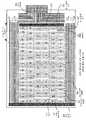
도 1a는 본 발명의 실시예들에 따른 기판의 단일 측면 상에 제조된 동일 평면상의 단일 층 터치 센서들을 갖는 예시적인 실질적으로 투명한 터치 센서 패널(100)의 부분도를 도시한다. 도 1a의 예에서는, (a 내지 h로 표기된) 8개의 칼럼 및 (1 내지 6으로 표기된) 6개의 로우를 갖는 터치 센서 패널(100)이 도시되어 있지만, 임의의 수의 칼럼 및 로우가 채용될 수 있다는 것을 이해해야 한다. 칼럼 a 내지 h는 일반적으로 모양이 칼럼 모양일 수 있지만, 도 1a의 예에서는, 각 칼럼의 하나의 측면이 각 칼럼에서 개별 섹션들을 생성하도록 설계된 갈지자형으로 된 에지들(staggered edges) 및 노치들(notches)을 포함한다. 로우 1 내지 6의 각각은 복수의 별개의 패치들 또는 패드들로부터 형성될 수 있고, 각 패치는 특정한 로우 내의 모든 패치들이 경계 영역들에서 연장하는 (도 1a에는 도시되지 않은) 금속 트레이스들을 통하여 함께 연결될 수 있게 하기 위해 터치 센서 패널(100)의 경계 영역에 라우팅되는 패치와 동일한 재료의 트레이스를 포함한다. 이 금속 트레이스들은 터치 센서 패널(100)의 하나의 측면 상의 작은 영역에 라우팅되고 플렉스 회로(102)에 연결된다. 도 1a의 예에서 도시된 바와 같이, 로우들을 형성하는 패치들은 일반적으로 파라미드 모양의 구성으로 배열될 수 있다. 도 1a에서, 예를 들면, 칼럼 a와 b 사이의 로우 1-3에 대한 패치들은 거꾸로 된 피라미드 구성으로 배열되어 있는 반면, 칼럼 a와 b 사이의 로우 4-6에 대한 패치들은 똑바로 선 파라미드 구성으로 배열되어 있다.1A shows a partial view of an exemplary substantially transparent touch sensor panel 100 having coplanar single layer touch sensors fabricated on a single side of a substrate in accordance with embodiments of the present invention. In the example of FIG. 1A, a touch sensor panel 100 is shown having eight columns (denoted a through h) and six rows (denoted 1 through 6), although any number of columns and rows may be employed. You must understand that you can. Columns a to h may generally be columnar in shape, but in the example of FIG. 1A, one side of each column has staggered edges and notches (designed to create individual sections in each column). notches). Each of
도 1a의 칼럼들 및 패치들은 전도성 재료의 동일 평면상의 단일 층에 형성될 수 있다. 터치 스크린 실시예들에서, 전도성 재료는 SITO(Single-layer Indium Tin Oxide)와 같은 실질적으로 투명한 재료일 수 있지만, 다른 재료들이 이용될 수도 있다. SITO 층은 커버 글라스의 뒷면에 또는 개별 기판의 상부에 형성될 수 있다. 비록 여기에서는 본 명세를 단순화하기 위하여 SITO가 참조될 수 있지만, 본 발명의 실시예들에 따라 다른 전도성 재료들이 이용될 수도 있다는 것을 이해해야 한다.The columns and patches of FIG. 1A may be formed in a single layer on the same plane of the conductive material. In touch screen embodiments, the conductive material may be a substantially transparent material such as Single-layer Indium Tin Oxide (SITO), although other materials may be used. The SITO layer can be formed on the back side of the cover glass or on top of the individual substrates. Although SITO may be referenced herein to simplify the present disclosure, it should be understood that other conductive materials may be used in accordance with embodiments of the present invention.
도 1b는 본 발명의 실시예들에 따른 터치 센서 패널의 경계 영역들에서 연장하는 금속 트레이스들(104 및 106)을 포함하는 예시적인 실질적으로 투명한 터치 센서 패널(100)의 부분도를 도시한다. 도 1b의 경계 영역들은 명료함을 위해 확대되어 있다는 것에 주목한다. 각 칼럼 a-h는 그 칼럼이 (도 1b에는 도시되지 않은) 비아를 통하여 금속 트레이스들에 연결되게 하는 SITO 트레이스(108)를 포함할 수 있다. 각 칼럼의 하나의 측면은 각 칼럼에서 개별 섹션들을 생성하도록 설계된 갈지자형으로 된 에지들(114) 및 노치들(116)을 포함한다. 각 로우 패치(1-6)는 그 패치가 (도 1b에는 도시되지 않은) 비아를 통하여 금속 트레이스에 연결되게 하는 SITO 트레이스(110)를 포함할 수 있다. SITO 트레이스들(110)은 특정한 로우의 각 패치가 서로에 자기 연결(self-connect)되게 할 수 있다. 모든 금속 트레이스들(104 및 106)은 동일한 층에 형성되기 때문에, 그것들은 모두 동일한 플렉스 회로(102)에 라우팅될 수 있다.FIG. 1B shows a partial view of an exemplary substantially transparent touch sensor panel 100 that includes metal traces 104 and 106 extending at boundary regions of a touch sensor panel in accordance with embodiments of the present invention. Note that the boundary regions of FIG. 1B are enlarged for clarity. Each column a-h may include a
만약 터치 센서 패널(100)이 상호 정전용량 터치 센서 패널로서 작동된다면, 칼럼 a-h 또는 로우 1-6은 하나 이상의 자극 신호들에 의해 구동될 수 있고, 인접한 칼럼 영역들 및 로우 패치들 사이에 프린징 전계 라인들(fringing electric lines)이 형성될 수 있다. 도 1b에서는, 비록 칼럼 a와 로우 패치 1(a-1) 사이의 전계 라인들(112)만이 예시를 위하여 도시되어 있지만, 어떤 칼럼들 또는 로우들이 자극되고 있는지에 따라서 다른 인접한 칼럼 및 로우 패치들(예를 들면, a-2, b-4, g-5 등) 사이에 전계 라인들이 형성될 수 있다는 것을 이해해야 한다. 따라서, 각 칼럼-로우 패치 쌍(예를 들면, a-1, a-2, b-4, g-5 등)은 2-전극 픽셀 또는 센서를 나타낼 수 있고 그곳에서 드라이브 전극으로부터 센스 전극으로 전하가 결합될 수 있다. 손가락이 이 픽셀들 중 하나 위에 착지(touch down)할 때, 터치 센서 패널의 커버를 넘어서 연장하는 프린징 전계 라인들 중 일부가 그 손가락에 의해 차단되어, 센스 전극에 결합되는 전하의 양이 감소된다. 이러한 전하의 양의 감소는 터치의 결과의 "이미지"를 결정하는 것의 일부로서 검출될 수 있다. 도 1b에 도시된 것과 같은 상호 정전용량 터치 센서 패널 디자인들에서는, 개별 기준 접지가 요구되지 않으므로, 기판의 뒷면 상에, 또는 개별 기판 상에 제2의 층이 요구되지 않는다는 것에 주목해야 한다.If the touch sensor panel 100 is operated as a mutual capacitive touch sensor panel, column ah or rows 1-6 can be driven by one or more stimulus signals, fringing between adjacent column regions and row patches. Frequing electric lines can be formed. In FIG. 1B, although only
터치 센서 패널(100)은 또한 자기 정전용량 터치 센서 패널로서 작동될 수 있다. 그러한 실시예에서는, 기판의 뒷면 상에, 또는 패치들 및 칼럼들과 동일한 측면 상에 있지만 유전체에 의해 그 패치들 및 칼럼들로부터 분리되어, 또는 개별 기판 상에 기준 접지면(reference ground plane)이 형성될 수 있다. 자기 정전용량 터치 센서 패널에서, 각 픽셀 또는 센서는 손가락의 존재로 인해 변경될 수 있는 기준 접지에 대한 자기 정전용량을 갖는다. 자기 정전용량 실시예들에서, 칼럼 a-h의 자기 정전용량은 독립적으로 감지될 수 있고, 로우 1-6의 자기 정전용량도 독립적으로 감지될 수 있다.The touch sensor panel 100 can also be operated as a magnetic capacitive touch sensor panel. In such an embodiment, on the back side of the substrate or on the same side as the patches and columns but separated from the patches and columns by a dielectric, or on a separate substrate a reference ground plane Can be formed. In a self-capacitance touch sensor panel, each pixel or sensor has a magnetic capacitance with respect to reference ground that can change due to the presence of a finger. In self capacitance embodiments, the magnetic capacitance of columns a-h can be sensed independently, and the self capacitances of rows 1-6 can also be sensed independently.
도 1c는 본 발명의 실시예들에 따른 터치 센서 패널의 경계 영역 내의 금속 트레이스들로의 칼럼들 및 로우 패치들의 예시적인 연결을 도시한다. 도 1c는 도 1b에 도시된 "상세 A"를 나타내고, SITO 트레이스들(108 및 110)을 통하여 금속 트레이스들(118)에 연결된 칼럼 "a" 및 로우 패치들 4-6을 나타낸다. SITO 트레이스들(108 및 110)은 유전체 재료에 의해 금속 트레이스들(118)과 분리되기 때문에, 유전체 재료 내의 비아들(120)은 SITO 트레이스들이 금속 트레이스들에 연결되게 한다.1C illustrates an exemplary connection of columns and row patches to metal traces within a boundary area of a touch sensor panel in accordance with embodiments of the present invention. FIG. 1C shows “Detail A” shown in FIG. 1B, and shows column “a” and row patches 4-6 connected to metal traces 118 via SITO traces 108 and 110. Since the SITO traces 108 and 110 are separated from the metal traces 118 by the dielectric material, the
도 2a는 본 발명의 실시예들에 따른 유전체 재료(222) 내의 비아(220)를 통하여 연결된 SITO 트레이스들(208) 및 금속 트레이스들(218)을 나타내는 터치 센서 패널(200)의 예시적인 단면을 도시한다. 도 2a는 도 1c에 도시된 뷰(view) B-B를 나타낸다.2A illustrates an exemplary cross-section of a
도 2b는 본 발명의 실시예들에 따른 도 2a에 도시된 예시적인 단면의 근접도이다. 도 2b는 SITO 트레이스(208)가 최대 스퀘어(square)당 약 155 옴(155Ω/□ max)의 저항률을 갖는 하나의 예시적인 실시예를 나타낸다. 하나의 실시예에서, 유전체(222)는 약 1500 옹스트롬의 무기 SiO2일 수 있고, 그것은 보다 높은 온도에서 처리될 수 있고 따라서 SITO 층이 보다 높은 품질로 스퍼터링되게 한다. 다른 실시예에서, 유전체(222)는 약 3.0 미크론의 유기 중합체일 수 있다. 1500 옹스트롬의 무기 SiO2는 (SITO 트레이스(208)와 금속 트레이스들(218) 사이의) 교차 정전용량(crossover capacitance)가 문제가 되지 않도록 충분히 작은 터치 센서 패널들을 위하여 이용될 수 있다.FIG. 2B is a close-up view of the exemplary cross section shown in FIG. 2A in accordance with embodiments of the present invention. FIG. 2B illustrates one exemplary embodiment where the
(약 3.5" 이상의 대각선 치수를 갖는) 보다 큰 터치 센서 패널들에 대해서는, 교차 정전용량이 문제가 되어, 부분적으로만 보상될 수 있는 오류 신호를 생성할 수 있다. 따라서, 보다 큰 터치 센서 패널들에 대해서는, 교차 정전용량을 낮추기 위해 약 3.0 미크론의 유기 중합체와 같은 보다 낮은 유전율을 갖는 보다 두꺼운 유전체 층(222)이 이용될 수 있다. 그러나, 보다 두꺼운 유전체 층의 이용은 SITO 층이 보다 낮은 온도에서 스퍼터링되도록 강제하여, 보다 낮은 광학 품질 및 보다 높은 저항률을 초래할 수 있다.For larger touch sensor panels (with a diagonal dimension of greater than about 3.5 "), cross capacitance is a problem, which can produce an error signal that can only be partially compensated. Therefore, larger touch sensor panels For lowering dielectric constants, thicker
다시 도 1c의 예를 참조하면, 칼럼 에지들(114) 및 로우 패치 4-6은 로우 패치 4 및 5를 연결하는 SITO 트레이스들(110)을 위하여 공간이 만들어져야 하기 때문에 갈지자형으로 될 수 있다. (도 1c의 예에서 로우 패치 4는 실제로는 함께 달라붙은 2개의 패치들이라는 것을 이해해야 한다.) 최저의 터치 감도를 획득하기 위하여, 픽셀들 a-6, a-5 및 a-4 내의 전극들의 면적의 균형을 맞추는 것이 바람직할 수 있다. 그러나, 만약 칼럼 "a"가 선형으로 유지된다면, 로우 패치 6은 로우 패치 5 또는 6보다 가늘어질 수 있고, 픽셀 a-6의 전극들 사이에 불균형이 생성될 수 있을 것이다.Referring back to the example of FIG. 1C, the column edges 114 and row patches 4-6 may be ragged because space must be made for the SITO traces 110 connecting
도 3은 본 발명의 실시예들에 따른 예시적인 칼럼 및 인접한 로우 패치들의 상면도를 도시한다. 일반적으로 터치 감지 회로의 범위 내에 머무르는 비교적 균일한 z-방향 터치 감도를 생성하기 위해 픽셀들 a-4, a-5 및 a-6의 상호 정전용량 특성들을 비교적 일정하게 만드는 것이 바람직할 수 있다. 따라서, 칼럼 영역들 a4, a5 및 a6는 로우 패치 영역들 4, 5 및 6과 거의 동일해야 한다. 이것을 달성하기 위해, 칼럼 세그먼트 a4의 면적이 칼럼 세그먼트들 a5 및 a6의 면적과 대등하도록 칼럼 섹션 a4 및 a5, 및 로우 패치 4 및 5는 컬럼 섹션 a6 및 로우 패치 6과 비교하여 y-방향으로 축소되어야 한다. 바꾸어 말하면, 픽셀 a4-4는 픽셀 a6-6보다 더 폭이 넓지만 더 짧을 것이고, 픽셀 a6-6은 더 폭이 좁지만 더 길 것이다.3 shows a top view of an exemplary column and adjacent row patches in accordance with embodiments of the present invention. It may be desirable to make the mutual capacitance characteristics of pixels a-4, a-5, and a-6 relatively constant to produce a relatively uniform z-direction touch sensitivity that generally remains within the range of the touch sensing circuit. Thus, column regions a4 , a5 and a6 should be nearly identical to row
전술한 도면들로부터 원시의 공간 감도는 다소 왜곡될 수 있다는 것이 명백할 것이다. 바꾸어 말하면, 픽셀들 또는 센서들은 x-방향으로 약간 빗나가게 되거나(skewed) 오정렬될(misaligned) 수 있기 때문에, 픽셀 a-6 상의 최대화된 터치 이벤트(예를 들면, 픽셀 a-6 바로 위에 놓인 손가락)의 x-좌표는, 예를 들면, 픽셀 a-4 상의 최대화된 터치 이벤트의 x-좌표와 약간 다를 수 있다. 따라서, 본 발명의 실시예들에서 이러한 오정렬은 픽셀들을 다시 매핑하고(re-map) 왜곡을 제거하기 위해 소프트웨어 알고리즘에서 디웝(de-warp)될 수 있다.It will be apparent from the above drawings that the original spatial sensitivity may be somewhat distorted. In other words, since the pixels or sensors may be slightly skewed or misaligned in the x-direction, a maximized touch event on pixel a-6 (eg, a finger directly above pixel a-6). The x-coordinate of may be slightly different from the x-coordinate of the maximized touch event on pixel a-4, for example. Thus, in embodiments of the present invention such misalignment may be de-warp in a software algorithm to re-map pixels and remove distortion.
비록 일반적인 터치 패널 그리드 치수는 5.0 mm 중심들에 배열된 픽셀들을 가질 수 있지만, 터치 센서 패널에서의 전기 연결들의 전체 수를 감소시키기 위해, 예를 들면, 약 6.0 mm 중심들을 갖는 더 많이 펼쳐진 그리드(more spread-out grid)가 바람직할 수 있다. 그러나, 센서 패턴을 펼치는 것은 잘못된 터치 판독들을 야기시킬 수 있다.Although typical touch panel grid dimensions may have pixels arranged at 5.0 mm centers, a more expanded grid (eg, about 6.0 mm centers) may be used to reduce the overall number of electrical connections in the touch sensor panel. more spread-out grids may be desirable. However, unfolding the sensor pattern can cause false touch readings.
도 4a는 넓은 간격들을 갖는 단일 로우 내의 2개의 인접한 픽셀들 a-5 및 b-5에 대한 픽셀에서 관찰되는 손가락 터치의 x-좌표 대 상호 정전용량의 플롯이다. 도 4a에서, 플롯(400)은 손가락 터치가 왼쪽에서 오른쪽으로 연속적으로 이동할 때 픽셀 a-5에서 관찰되는 상호 정전용량을 나타내고, 플롯(402)은 손가락 터치가 왼쪽에서 오른쪽으로 연속적으로 이동할 때 픽셀 b-5에서 관찰되는 상호 정전용량을 나타낸다. 예상되는 바와 같이, 손가락 터치가 픽셀 a-5의 바로 위에 지나갈 때 픽셀 a-5에서 상호 정전용량의 하락(404)이 관찰되고, 손가락 터치가 픽셀 b-5의 바로 위에 지나갈 때 픽셀 b-5에서 상호 정전용량의 유사한 하락(406)이 관찰된다. 만약 라인(408)이 터치 이벤트를 검출하기 위한 임계치를 나타낸다면, 도 4a는 손가락이 터치 센서 패널의 표면으로부터 결코 들어올려지지 않더라도, 410에서 손가락이 순간적으로 표면에서 들어올려진 것같이 잘못 보일 수 있다. 이 위치(410)는 2개의 펼쳐진 픽셀들 사이의 약 중간 지점을 나타낼 수 있다.4A is a plot of the x-coordinate versus mutual capacitance of a finger touch observed in a pixel for two adjacent pixels a-5 and b-5 in a single row with wide spacings. In FIG. 4A,
도 4b는 본 발명의 실시예들에 따른 공간 보간(spatial interpolation)이 제공된 넓은 간격들을 갖는 단일 로우 내의 2개의 인접한 픽셀들 a-5 및 b-5에 대한 픽셀에서 관찰되는 손가락 터치의 x-좌표 대 상호 정전용량의 플롯이다. 예상되는 바와 같이, 손가락 터치가 픽셀 a-5의 바로 위에 지나갈 때 픽셀 a-5에서 상호 정전용량의 하락(404)이 관찰되고, 손가락 터치가 픽셀 b-5의 바로 위에 지나갈 때 픽셀 b-5에서 상호 정전용량의 유사한 하락(406)이 관찰된다. 그러나, 상호 정전용량의 상승 및 하락은 도 4a에서보다 더 점진적으로 일어난다는 것에 주목한다. 만약 라인(408)이 터치 이벤트를 검출하기 위한 임계치를 나타낸다면, 도 4b는 손가락이 왼쪽에서 오른쪽으로 픽셀 a-5 및 b-5 위로 이동할 때, 픽셀 a-5 또는 b-5의 어느 쪽에서든 항상 터치 이벤트가 검출된다. 바꾸어 말하면, 터치 이벤트들의 이 "블러링"(blurring)은 그릇된 논-터치 판독들(false non-touch readings)이 나타나는 것을 방지하는 데 도움이 된다.4b is the x-coordinate of the finger touch observed in the pixel for two adjacent pixels a-5 and b-5 in a single row with wide spacings provided with spatial interpolation according to embodiments of the present invention. Plot of mutual capacitance. As expected, a drop in
본 발명의 하나의 실시예에서, 터치 센서 패널을 위한 커버 글라스의 두께는 도 4b에 도시된 공간 블러링 또는 필터링의 일부 또는 전부를 생성하기 위해 증가될 수 있다.In one embodiment of the invention, the thickness of the cover glass for the touch sensor panel can be increased to produce some or all of the spatial blurring or filtering shown in FIG. 4B.
도 4c는 본 발명의 실시예들에 따른 보다 큰 픽셀 간격들에 대하여 유용한 예시적인 칼럼 및 인접한 로우 패치 패턴의 상면도를 도시한다. 도 4c는 x-방향으로 연장(elongate)된 픽셀 내에서 톱니 전극 에지들(412)이 채용되는 예시적인 실시예를 도시한다. 톱니 전극 에지들은 x-방향으로 보다 큰 거리에 걸쳐서 동일한 픽셀에 의해 터치 이벤트가 검출될 수 있도록 x-방향으로 보다 큰 영역에 걸쳐서 필터링 전계 라인들(414)이 존재하게 할 수 있다. 도 4c의 톱니 구성은 단지 예시적인 것이고, 뱀 모양의 에지 등과 같은 다른 구성들도 이용될 수 있다는 것을 이해해야 한다. 이러한 구성들은 터치 패턴들을 더욱 부드럽게 하고 도 4b에 도시된 바와 같이 인접한 픽셀들 사이에 추가적인 공간 필터링 및 보간을 생성할 수 있다.4C shows a top view of an exemplary column and adjacent low patch pattern useful for larger pixel intervals in accordance with embodiments of the present invention. 4C shows an example embodiment in which the sawtooth electrode edges 412 are employed in a pixel elongated in the x-direction. The sawtooth electrode edges may cause the
도 5는 본 발명의 실시예들에 따른 커버 글라스에 접합된 터치 센서 패널 기판 상의 SITO의 예시적인 스택업(stackup)을 도시한다. 스택업은 글라스로 형성될 수 있는 터치 센서 패널 기판(500)을 포함할 수 있고, 그 위에 하나의 측면 상에는 AR(anti-reflective) 막(510)이 형성될 수 있고 다른 측면 상에는 경계 영역들 내의 버스 라인들을 형성하도록 금속(502)이 증착될 수 있다. 금속(502)은 최대 스퀘어당 0.8 옴(0.8Ω/□ max)의 저항률을 가질 수 있다. 그 후 기판(500) 및 금속(502) 위에 절연층(504)이 증착될 수 있다. 절연층은, 예를 들면, 1500 옹스트롬의 두께를 갖는 SiO2, 또는 3 미크론의 유기 중합체일 수 있다. 절연체(504) 내에 비아(506)들을 형성하기 위해 포토리소그래피가 이용될 수 있고, 그 후 절연체 및 금속(502)의 위에 전도성 재료(508)가 증착되고 패터닝될 수 있다. 최대 스퀘어당 155 옴의 저항률을 갖는 ITO와 같은 투명한 전도성 재료로부터 형성될 수 있는 전도성 재료(508)의 단일 층은 다중 층 디자인들보다 더 투명할 수 있고, 제조하기가 더 용이할 수 있다. ACF(anisotropic conductive film)와 같은 접착제(514)를 이용하여 전도성 재료(508) 및 금속(502)에 플렉스 회로(512)가 접합될 수 있다. 그 후 전체 서브어셈블리는 PSA(pressure sensitive adhesive)와 같은 접착제(518)를 이용하여 커버 글라스(516) 및 블랙마스크(520)에 접합될 수 있다.5 illustrates an exemplary stackup of SITO on a touch sensor panel substrate bonded to a cover glass in accordance with embodiments of the present invention. The stackup may include a touch
대안 실시예에서, 전술한 금속, 절연체, 전도성 재료는 커버 글라스의 뒷면 상에 형성될 수 있다.In alternative embodiments, the metals, insulators, and conductive materials described above may be formed on the back side of the cover glass.
도 6은 이 발명의 실시예들에 따른 전술한 터치 센서 패널과 함께 동작 가능한 예시적인 컴퓨팅 시스템(600)을 도시한다. 터치 센서 패널(624) 및 디스플레이 장치(640)(예를 들면, LCD 모듈)를 포함할 수 있는 터치스크린(642)은 센서 패널 상에 일체로 형성된 커넥터들을 통하여, 또는 플렉스 회로들을 이용하여 컴퓨팅 시스템(600) 내의 다른 컴포넌트들에 연결될 수 있다. 컴퓨팅 시스템(600)은 하나 이상의 패널 프로세서(602) 및 주변 장치들(peripherals)(604), 및 패널 서브시스템(606)을 포함할 수 있다. 하나 이상의 프로세서(602)는, 예를 들면, ARM968 프로세서 또는 유사한 기능 및 성능을 갖는 다른 프로세서를 포함할 수 있다. 그러나, 다른 실시예들에서, 패널 프로세서 기능은 대신에 상태 기계와 같은 전용 로직에 의해 구현될 수 있다. 주변 장치들(604)은 RAM(random access memory) 또는 다른 종류의 메모리 또는 저장 장치, 감시 타이머(watchdog timer) 등을 포함할 수 있지만, 이에 제한되지는 않는다.6 illustrates an
패널 서브시스템(606)은, 하나 이상의 아날로그 채널(608), 채널 스캔 로직(610) 및 드라이버 로직(614)을 포함할 수 있지만, 이에 제한되지는 않는다. 채널 스캔 로직(610)은 RAM(612)에 액세스하고, 아날로그 채널들로부터 자율적으로 데이터를 판독하고 아날로그 채널들에 대한 제어를 제공할 수 있다. 이 제어는 터치 센서 패널(624)의 센스 라인들을 아날로그 채널들(608)에 멀티플렉싱하는 것 또는 다른 방법으로 연결하는 것을 포함할 수 있다. 또한, 채널 스캔 로직(610)은 터치 센서 패널(624)의 드라이브 라인들에 선택적으로 인가되는 드라이버 로직 및 자극 신호들을 제어할 수 있다. 일부 실시예들에서, 패널 서브시스템(606), 패널 프로세서(602) 및 주변 장치들(604)은 하나의 ASIC(application specific integrated circuit) 내에 통합될 수 있다.
드라이버 로직(614)은 다수의 패널 서브시스템 출력들(616)을 제공할 수 있고 고전압 드라이버(618)를 구동하는 독점 인터페이스(proprietary interface)를 제공할 수 있다. 고전압 드라이버(618)는 저전압 레벨(예를 들면, CMOS(complementary metal oxide semiconductor) 레벨들)로부터, 잡음 감소를 위한 보다 나은 S/N(signal-to-noise) 비를 제공하는, 보다 높은 전압 레벨로 시프팅하는 레벨을 제공할 수 있다. 패널 서브시스템 출력들(616)은 디코더(620) 및 레벨 시프터/드라이버(638)에 보내질 수 있고, 레벨 시프터/드라이버(638)는 하나 이상의 고전압 드라이버 출력들을 독점 인터페이스를 통하여 하나 이상의 패널 로우 또는 드라이브 라인 입력들(622)에 선택적으로 연결하고 고전압 드라이버(618)에서 보다 적은 수의 고전압 드라이버 회로들의 이용을 가능하게 할 수 있다. 각 패널 로우 입력(622)은 터치 센서 패널(624) 내의 하나 이상의 드라이브 라인을 구동할 수 있다. 일부 실시예들에서, 고전압 드라이버(618) 및 디코더(620)는 하나의 ASIC 내에 통합될 수 있다. 그러나, 다른 실시예들에서 고전압 드라이버(618) 및 디코더(620)는 드라이버 로직(614) 내에 통합될 수 있고, 또 다른 실시예들에서 고전압 드라이버(618) 및 디코더(620)는 완전히 제거될 수 있다.Driver logic 614 may provide a number of panel subsystem outputs 616 and may provide a proprietary interface for driving
컴퓨팅 시스템(600)은 또한 패널 프로세서(602)로부터의 출력들을 수신하고 그 출력에 기초하여 액션들을 수행하기 위한 호스트 프로세서(628)를 포함할 수 있고, 그 액션들은, 커서 또는 포인터와 같은 개체를 움직이는 것, 스크롤링하는 것 또는 패닝하는 것(panning), 제어 설정을 조정하는 것, 파일 또는 문서를 여는 것, 메뉴를 보는 것, 선택을 하는 것, 명령을 실행하는 것, 호스트 장치에 연결된 주변 장치를 조작하는 것, 전화 통화를 받는 것, 전화 통화를 거는 것, 전화 통화를 종료하는 것, 볼륨 또는 오디오 설정을 변경하는 것, 주소들, 자주 다이얼링되는 번호들, 수신 통화들, 받지 못한 통화들과 같은 전화 통신과 관련된 정보를 저장하는 것, 컴퓨터 또는 컴퓨터 네트워크에 로그온하는 것, 허가된 개인들에게 컴퓨터 또는 컴퓨터 네트워크의 제한된 영역들에의 액세스를 허용하는 것, 컴퓨터 데스크톱의 사용자의 선호 배열과 관련된 사용자 프로파일을 로딩하는 것, 웹 콘텐트에의 액세스를 허용하는 것, 특정 프로그램을 시작하는 것, 메시지를 암호화하거나 해독하는 것 등을 포함할 수 있지만, 이에 제한되지는 않는다. 호스트 프로세서(628)는 또한 패널 처리에 관련되지 않을 수 있는 추가적인 기능들을 수행할 수 있고, 장치의 사용자에게 사용자 인터페이스(UI)를 제공하기 위해 LCD와 같은 디스플레이 장치(640) 및 프로그램 저장 장치(632)에 연결될 수 있다.
전술한 터치 센서 패널은 비용이 더 낮고, 제조가 더 용이하고, 기존의 기계 제어 아우트라인에 적합한 공간 효율적인 터치 센서 패널 및 UI를 제공하기 위해 도 6의 시스템에서 유리하게 이용될 수 있다.The aforementioned touch sensor panel can be advantageously used in the system of FIG. 6 to provide a lower cost, easier to manufacture, and a space efficient touch sensor panel and UI suitable for existing machine control outlines.
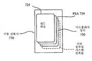
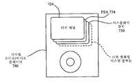
도 7a는 본 발명의 실시예들에 따른 (옵션으로 PSA(734)를 이용하여 함께 접합된) 터치 센서 패널(724) 및 디스플레이 장치(730) 스택업들 및 전술한 컴퓨팅 시스템을 포함할 수 있는 예시적인 이동 전화기(736)를 도시한다. 도 7b는 본 발명의 실시예들에 따른 (옵션으로 PSA(734)를 이용하여 함께 접합된) 터치 센서 패널(724) 및 디스플레이 장치(730) 스택업들 및 전술한 컴퓨팅 시스템을 포함할 수 있는 예시적인 디지털 오디오/비디오 플레이어(740)를 도시한다. 도 7a 및 7b의 이동 전화기 및 디지털 오디오/비디오 플레이어는 전술한 터치 센서 패널들로부터 유리하게 이익을 얻을 수 있는데, 그 이유는 그 터치 센서 패널은 이들 장치들이 더 작고 비용이 적게 들게 할 수 있고, 이것은 소비자 호감 및 상업적 성공에 상당한 영향을 미칠 수 있는 중요한 소비자 요인들이기 때문이다.FIG. 7A may include a
비록 이 발명의 실시예들은 첨부 도면들에 관련하여 충분히 설명되었지만, 이 기술 분야의 숙련자들에게는 다양한 변경들 및 수정들이 명백할 것이라는 점에 주목해야 한다. 그러한 변경들 및 수정들은 첨부된 청구항들에 의해 한정되는 이 발명의 실시예들의 범위 내에 포함되는 것으로 이해되어야 한다.Although embodiments of this invention have been described fully with reference to the accompanying drawings, it should be noted that various changes and modifications will be apparent to those skilled in the art. Such changes and modifications are to be understood as being included within the scope of embodiments of the invention as defined by the appended claims.
Claims (33)
Translated fromKorean단일 층 상에 형성되고 기판의 한 측면 상에 지지되는 전도성 재료의 복수의 칼럼들(columns); 및
상기 복수의 칼럼들과 동일한 상기 기판의 측면 상에 지지되는 상기 전도성 재료의 복수의 패치들(patches) ? 상기 복수의 패치들은 상기 복수의 칼럼들에 인접하여 상기 복수의 칼럼들과 동일한 층 상에 형성되고 복수의 로우들(rows)에 배열되고, 특정한 로우 내의 각 패치는 상기 복수의 칼럼들 및 패치들과 동일한 층 상에 형성된 연결 트레이스들(connecting traces)에 의해 함께 연결됨 ?
을 포함하고,
상기 복수의 패치들의 각 패치와 상기 복수의 칼럼들의 각 칼럼은 정전용량 센서(capacitive sensor)의 일부를 형성하는 터치 센서 패널.As a touch sensor panel,
A plurality of columns of conductive material formed on a single layer and supported on one side of the substrate; And
A plurality of patches of conductive material supported on the same side of the substrate as the plurality of columns; The plurality of patches are formed on the same layer as the plurality of columns adjacent to the plurality of columns and arranged in a plurality of rows, each patch in a particular row being the plurality of columns and patches. Connected together by connecting traces formed on the same layer as
Including,
Wherein each patch of the plurality of patches and each column of the plurality of columns form part of a capacitive sensor.
로우에 배열된 각 복수의 패치들은 상기 접지면과 함께 자기 정전용량 센서(self-capacitance sensor)를 형성하고, 상기 복수의 칼럼들의 각 칼럼은 상기 접지면과 함께 자기 정전용량 센서를 형성하는 터치 센서 패널.The method of claim 1, further comprising a ground plane supported on the substrate,
Each of the plurality of patches arranged in a row forms a self-capacitance sensor with the ground plane, and each column of the plurality of columns forms a self-capacitance sensor with the ground plane. panel.
The touch sensor panel of claim 1, wherein the touch sensor panel is integrated into a mobile computing system.
기판의 한 측면 상의 단일 층 상에 전도성 재료의 복수의 칼럼들(columns)을 형성하는 단계;
상기 복수의 칼럼들과 동일한 상기 기판의 측면 상에 상기 복수의 칼럼들에 인접하여 상기 복수의 칼럼들과 동일한 층 상에 복수의 로우들(rows)에 배열된 상기 전도성 재료의 복수의 패치들(patches)을 형성하는 단계;
특정한 로우 내의 각 패치를 상기 복수의 칼럼들 및 패치들과 동일한 층 상에 형성된 연결 트레이스들(connecting traces)에 의해 함께 연결하는 단계; 및
상기 복수의 패치들의 각 패치와 상기 복수의 칼럼들의 각 칼럼으로부터 정전용량 센서(capacitive sensor)의 일부를 형성하는 단계
를 포함하는 방법.As a method of forming a touch sensor panel,
Forming a plurality of columns of conductive material on a single layer on one side of the substrate;
A plurality of patches of conductive material arranged in a plurality of rows on the same layer as the plurality of columns adjacent to the plurality of columns on the side of the substrate that are identical to the plurality of columns ( forming patches);
Connecting each patch in a particular row together by connecting traces formed on the same layer as the plurality of columns and patches; And
Forming a portion of a capacitive sensor from each patch of the plurality of patches and each column of the plurality of columns
How to include.
상기 기판 상에 접지면을 형성하는 단계; 및
상기 접지면과 함께 로우에 배열된 각 복수의 패치들로부터, 및 상기 접지면과 함께 상기 복수의 칼럼들의 각 칼럼으로부터 자기 정전용량 센서(self-capacitance sensor)를 형성하는 단계를 더 포함하는 방법.The method of claim 18,
Forming a ground plane on the substrate; And
Forming a self-capacitance sensor from each of the plurality of patches arranged in a row with the ground plane, and from each column of the plurality of columns with the ground plane.
Applications Claiming Priority (5)
| Application Number | Priority Date | Filing Date | Title |
|---|---|---|---|
| US97762107P | 2007-10-04 | 2007-10-04 | |
| US60/977,621 | 2007-10-04 | ||
| US12/038,760US8633915B2 (en) | 2007-10-04 | 2008-02-27 | Single-layer touch-sensitive display |
| US12/038,760 | 2008-02-27 | ||
| PCT/US2008/078836WO2009046363A1 (en) | 2007-10-04 | 2008-10-03 | Single-layer touch-sensitive display |
Related Child Applications (1)
| Application Number | Title | Priority Date | Filing Date |
|---|---|---|---|
| KR1020117029375ADivisionKR101354390B1 (en) | 2007-10-04 | 2008-10-03 | Single-layer touch-sensitive display |
Publications (2)
| Publication Number | Publication Date |
|---|---|
| KR20100091173A KR20100091173A (en) | 2010-08-18 |
| KR101123542B1true KR101123542B1 (en) | 2012-03-14 |
Family
ID=39951922
Family Applications (5)
| Application Number | Title | Priority Date | Filing Date |
|---|---|---|---|
| KR1020107009798AExpired - Fee RelatedKR101123542B1 (en) | 2007-10-04 | 2008-10-03 | Single-layer touch-sensitive display |
| KR1020117029375AExpired - Fee RelatedKR101354390B1 (en) | 2007-10-04 | 2008-10-03 | Single-layer touch-sensitive display |
| KR1020147037073AExpired - Fee RelatedKR101597483B1 (en) | 2007-10-04 | 2008-10-03 | Single-layer touch-sensitive display |
| KR1020157017451AActiveKR101733902B1 (en) | 2007-10-04 | 2008-10-03 | Single-layer touch-sensitive display |
| KR1020127033882AActiveKR101530767B1 (en) | 2007-10-04 | 2008-10-03 | Single-layer touch-sensitive display |
Family Applications After (4)
| Application Number | Title | Priority Date | Filing Date |
|---|---|---|---|
| KR1020117029375AExpired - Fee RelatedKR101354390B1 (en) | 2007-10-04 | 2008-10-03 | Single-layer touch-sensitive display |
| KR1020147037073AExpired - Fee RelatedKR101597483B1 (en) | 2007-10-04 | 2008-10-03 | Single-layer touch-sensitive display |
| KR1020157017451AActiveKR101733902B1 (en) | 2007-10-04 | 2008-10-03 | Single-layer touch-sensitive display |
| KR1020127033882AActiveKR101530767B1 (en) | 2007-10-04 | 2008-10-03 | Single-layer touch-sensitive display |
Country Status (14)
| Country | Link |
|---|---|
| US (5) | US8633915B2 (en) |
| EP (1) | EP2045698B1 (en) |
| JP (3) | JP2010541109A (en) |
| KR (5) | KR101123542B1 (en) |
| CN (4) | CN103019450B (en) |
| AT (1) | ATE463784T1 (en) |
| AU (1) | AU2008308465B2 (en) |
| CA (1) | CA2700909C (en) |
| DE (2) | DE602008000960D1 (en) |
| ES (1) | ES2344487T3 (en) |
| GB (1) | GB2453418B (en) |
| IL (1) | IL204859A (en) |
| TW (2) | TWI484398B (en) |
| WO (1) | WO2009046363A1 (en) |
Cited By (1)
| Publication number | Priority date | Publication date | Assignee | Title |
|---|---|---|---|---|
| US12386471B2 (en) | 2023-07-10 | 2025-08-12 | Samsung Display Co., Ltd. | Touch panel and display device including the same |
Families Citing this family (229)
| Publication number | Priority date | Publication date | Assignee | Title |
|---|---|---|---|---|
| US7663607B2 (en) | 2004-05-06 | 2010-02-16 | Apple Inc. | Multipoint touchscreen |
| CN102981678B (en)* | 2006-06-09 | 2015-07-22 | 苹果公司 | Touch screen liquid crystal display |
| US8633915B2 (en) | 2007-10-04 | 2014-01-21 | Apple Inc. | Single-layer touch-sensitive display |
| TWI374379B (en) | 2007-12-24 | 2012-10-11 | Wintek Corp | Transparent capacitive touch panel and manufacturing method thereof |
| US20090174676A1 (en) | 2008-01-04 | 2009-07-09 | Apple Inc. | Motion component dominance factors for motion locking of touch sensor data |
| TWM348999U (en)* | 2008-02-18 | 2009-01-11 | Tpk Touch Solutions Inc | Capacitive touch panel |
| US9007310B1 (en)* | 2008-02-29 | 2015-04-14 | Cypress Semiconductor Corporation | Single layer touch sensor with improved sensitivity and accuracy |
| JP4816668B2 (en)* | 2008-03-28 | 2011-11-16 | ソニー株式会社 | Display device with touch sensor |
| US8487898B2 (en) | 2008-04-25 | 2013-07-16 | Apple Inc. | Ground guard for capacitive sensing |
| US8576193B2 (en)* | 2008-04-25 | 2013-11-05 | Apple Inc. | Brick layout and stackup for a touch screen |
| US9069418B2 (en) | 2008-06-06 | 2015-06-30 | Apple Inc. | High resistivity metal fan out |
| US8673163B2 (en)* | 2008-06-27 | 2014-03-18 | Apple Inc. | Method for fabricating thin sheets of glass |
| US8120371B2 (en)* | 2008-06-27 | 2012-02-21 | Synaptics, Inc. | Object position sensing apparatus |
| US7810355B2 (en) | 2008-06-30 | 2010-10-12 | Apple Inc. | Full perimeter chemical strengthening of substrates |
| US20100059294A1 (en)* | 2008-09-08 | 2010-03-11 | Apple Inc. | Bandwidth enhancement for a touch sensor panel |
| US8624845B2 (en)* | 2008-09-26 | 2014-01-07 | Cypress Semiconductor Corporation | Capacitance touch screen |
| US8368657B2 (en)* | 2008-12-01 | 2013-02-05 | Freescale Semiconductor, Inc. | Touch sensor panel using regional and local electrodes to increase number of sense locations |
| US8319747B2 (en) | 2008-12-11 | 2012-11-27 | Apple Inc. | Single layer touch panel with segmented drive and sense electrodes |
| TW201025108A (en)* | 2008-12-31 | 2010-07-01 | Acrosense Technology Co Ltd | Capacitive touch panel |
| US7918019B2 (en)* | 2009-01-09 | 2011-04-05 | Apple Inc. | Method for fabricating thin touch sensor panels |
| US9063605B2 (en) | 2009-01-09 | 2015-06-23 | Apple Inc. | Thin glass processing using a carrier |
| US8922521B2 (en) | 2009-02-02 | 2014-12-30 | Apple Inc. | Switching circuitry for touch sensitive display |
| US9261997B2 (en)* | 2009-02-02 | 2016-02-16 | Apple Inc. | Touch regions in diamond configuration |
| US20100214247A1 (en)* | 2009-02-20 | 2010-08-26 | Acrosense Technology Co., Ltd. | Capacitive Touch Panel |
| US20110019354A1 (en)* | 2009-03-02 | 2011-01-27 | Christopher Prest | Techniques for Strengthening Glass Covers for Portable Electronic Devices |
| CN102388003B (en) | 2009-03-02 | 2014-11-19 | 苹果公司 | Technology for Strengthening Glass Covers for Portable Electronic Devices |
| JP5493739B2 (en)* | 2009-03-19 | 2014-05-14 | ソニー株式会社 | Sensor device and information processing device |
| US8982051B2 (en)* | 2009-03-30 | 2015-03-17 | Microsoft Technology Licensing, Llc | Detecting touch on a surface |
| US9317140B2 (en)* | 2009-03-30 | 2016-04-19 | Microsoft Technology Licensing, Llc | Method of making a multi-touch input device for detecting touch on a curved surface |
| US8593410B2 (en) | 2009-04-10 | 2013-11-26 | Apple Inc. | Touch sensor panel design |
| US8624849B2 (en)* | 2009-04-20 | 2014-01-07 | Apple Inc. | Touch actuated sensor configuration integrated with an OLED structure |
| US20100265187A1 (en)* | 2009-04-20 | 2010-10-21 | Shih Chang Chang | Signal routing in an oled structure that includes a touch actuated sensor configuration |
| US8599565B2 (en) | 2009-04-21 | 2013-12-03 | Fujitsu Component Limited | Touchscreen panel, electronic apparatus and method of fabricating touchscreen panel |
| US8911653B2 (en) | 2009-05-21 | 2014-12-16 | Semiconductor Energy Laboratory Co., Ltd. | Method for manufacturing light-emitting device |
| US8279194B2 (en) | 2009-05-22 | 2012-10-02 | Elo Touch Solutions, Inc. | Electrode configurations for projected capacitive touch screen |
| US9075484B2 (en)* | 2009-06-02 | 2015-07-07 | Pixart Imaging Inc. | Sensor patterns for mutual capacitance touchscreens |
| US9372536B2 (en)* | 2009-06-05 | 2016-06-21 | Empire Technology Development Llc | Touch screen with tactile feedback |
| US8576161B2 (en)* | 2009-06-18 | 2013-11-05 | Apple Inc. | Driving an OLED display structure integrated with a touch sensor configuration |
| US8711108B2 (en)* | 2009-06-19 | 2014-04-29 | Apple Inc. | Direct connect single layer touch panel |
| US8957874B2 (en) | 2009-06-29 | 2015-02-17 | Apple Inc. | Touch sensor panel design |
| US20110005662A1 (en)* | 2009-07-10 | 2011-01-13 | Kuo-Hua Sung | Method for Fabricating Multilayer Panels |
| US20110018829A1 (en)* | 2009-07-24 | 2011-01-27 | Cypress Semiconductor Corporation | Mutual capacitance sensing array |
| US9753597B2 (en) | 2009-07-24 | 2017-09-05 | Cypress Semiconductor Corporation | Mutual capacitance sensing array |
| US8477106B2 (en) | 2009-07-29 | 2013-07-02 | Elo Touch Solutions, Inc. | System and method for a projected capacitive touchscreen having weight based coordinate determination |
| US8415958B2 (en) | 2009-09-11 | 2013-04-09 | Synaptics Incorporated | Single layer capacitive image sensing |
| JP2013504819A (en)* | 2009-09-11 | 2013-02-07 | シナプティクス インコーポレイテッド | Input device based on voltage gradient |
| TWI408580B (en)* | 2009-10-30 | 2013-09-11 | Hannstar Display Corp | Projective capacitive touch sensor |
| JP5371712B2 (en)* | 2009-11-26 | 2013-12-18 | 京セラ株式会社 | Key input device and portable terminal |
| CN102081484B (en)* | 2009-11-30 | 2013-01-09 | 上海天马微电子有限公司 | Capacitive touch sensing device, forming method thereof and touch display device |
| US20110134050A1 (en)* | 2009-12-07 | 2011-06-09 | Harley Jonah A | Fabrication of touch sensor panel using laser ablation |
| US9298303B2 (en)* | 2009-12-31 | 2016-03-29 | Google Technology Holdings LLC | Duty cycle modulation of periodic time-synchronous receivers for noise reduction |
| US9778685B2 (en) | 2011-05-04 | 2017-10-03 | Apple Inc. | Housing for portable electronic device with reduced border region |
| CN102141865B (en)* | 2010-02-02 | 2012-11-28 | 展触光电科技股份有限公司 | Single-layer projected capacitive touch panel and manufacturing method thereof |
| CN102915168B (en)* | 2010-02-02 | 2016-03-23 | 宸鸿光电科技股份有限公司 | single-layer projected capacitive touch panel |
| DE102010014796A1 (en) | 2010-02-03 | 2011-08-04 | Emerging Display Technologies Corp. | Screen unit with a touch screen |
| CN102193700B (en)* | 2010-03-15 | 2015-07-08 | 上海天马微电子有限公司 | Touch screen |
| TWI615743B (en)* | 2010-03-25 | 2018-02-21 | Winsky Tech Limited | Touch panel and method of manufacturing same |
| TWI412970B (en)* | 2010-03-30 | 2013-10-21 | Chunghwa Picture Tubes Ltd | Touch input device |
| US9203489B2 (en) | 2010-05-05 | 2015-12-01 | Google Technology Holdings LLC | Method and precoder information feedback in multi-antenna wireless communication systems |
| US8975536B2 (en)* | 2010-05-14 | 2015-03-10 | Sharp Kabushiki Kaisha | Wiring structure, display panel, and display device |
| JP2013526746A (en)* | 2010-05-14 | 2013-06-24 | イーロ・タッチ・ソリューションズ・インコーポレイテッド | System and method for detecting the position of a touch on a touch sensor |
| US9727175B2 (en) | 2010-05-14 | 2017-08-08 | Elo Touch Solutions, Inc. | System and method for detecting locations of touches on a projected capacitive touch sensor |
| US9213451B2 (en) | 2010-06-04 | 2015-12-15 | Apple Inc. | Thin glass for touch panel sensors and methods therefor |
| KR20110121661A (en)* | 2010-07-02 | 2011-11-08 | 삼성전기주식회사 | Touch panel |
| US9652088B2 (en) | 2010-07-30 | 2017-05-16 | Apple Inc. | Fabrication of touch sensor panel using laser ablation |
| US10189743B2 (en) | 2010-08-18 | 2019-01-29 | Apple Inc. | Enhanced strengthening of glass |
| JP5260607B2 (en)* | 2010-09-01 | 2013-08-14 | 双葉電子工業株式会社 | Touch sensor and fluorescent display tube |
| US8824140B2 (en) | 2010-09-17 | 2014-09-02 | Apple Inc. | Glass enclosure |
| US8950215B2 (en) | 2010-10-06 | 2015-02-10 | Apple Inc. | Non-contact polishing techniques for reducing roughness on glass surfaces |
| US9454268B2 (en) | 2010-10-12 | 2016-09-27 | Parade Technologies, Ltd. | Force sensing capacitive hybrid touch sensor |
| US9459736B2 (en)* | 2010-10-12 | 2016-10-04 | Parade Technologies, Ltd. | Flexible capacitive sensor array |
| US9491852B2 (en) | 2010-10-15 | 2016-11-08 | Apple Inc. | Trace border routing |
| JP5445438B2 (en)* | 2010-12-15 | 2014-03-19 | Smk株式会社 | Capacitive touch panel |
| KR101715858B1 (en)* | 2010-12-31 | 2017-03-13 | 엘지디스플레이 주식회사 | Apparatus for driving touch sensor |
| US10781135B2 (en) | 2011-03-16 | 2020-09-22 | Apple Inc. | Strengthening variable thickness glass |
| US9725359B2 (en) | 2011-03-16 | 2017-08-08 | Apple Inc. | Electronic device having selectively strengthened glass |
| TW201241711A (en)* | 2011-04-11 | 2012-10-16 | xiang-yu Li | Touch panel device with single-layer radial electrode layout |
| US9128666B2 (en) | 2011-05-04 | 2015-09-08 | Apple Inc. | Housing for portable electronic device with reduced border region |
| WO2012176966A1 (en)* | 2011-06-20 | 2012-12-27 | Melfas, Inc. | Touch sensor panel |
| EP2538313B1 (en) | 2011-06-20 | 2015-05-20 | Melfas, Inc. | Touch sensor panel |
| US8886480B2 (en) | 2011-06-27 | 2014-11-11 | Synaptics Incorporated | System and method for signaling in gradient sensor devices |
| KR101363361B1 (en)* | 2011-07-06 | 2014-02-14 | (주)멜파스 | Panel for sensing touch input |
| CN103733168B (en)* | 2011-07-22 | 2016-11-23 | 波利Ic有限及两合公司 | Capacitive Touch Area Device |
| DE102011108153A1 (en)* | 2011-07-22 | 2013-01-24 | Polyic Gmbh & Co. Kg | Multi-layer body |
| CN102902394A (en)* | 2011-07-28 | 2013-01-30 | 宸鸿科技(厦门)有限公司 | Touch panel and detecting method thereof |
| DE102011108803B4 (en) | 2011-07-29 | 2017-06-29 | Polyic Gmbh & Co. Kg | A plastic film touch sensor, use of the plastic film and method of making a multimodal input device |
| US9052782B2 (en) | 2011-07-29 | 2015-06-09 | Synaptics Incorporated | Systems and methods for voltage gradient sensor devices |
| US9944554B2 (en) | 2011-09-15 | 2018-04-17 | Apple Inc. | Perforated mother sheet for partial edge chemical strengthening and method therefor |
| US9516149B2 (en) | 2011-09-29 | 2016-12-06 | Apple Inc. | Multi-layer transparent structures for electronic device housings |
| WO2013049816A1 (en)* | 2011-09-30 | 2013-04-04 | Sensitronics, LLC | Hybrid capacitive force sensors |
| US20130100038A1 (en)* | 2011-10-20 | 2013-04-25 | Atmel Technologies U.K. Limited | Single-Layer Touch Sensor |
| KR101984161B1 (en) | 2011-11-08 | 2019-05-31 | 삼성전자 주식회사 | Touch screen panel and portable device |
| US10144669B2 (en) | 2011-11-21 | 2018-12-04 | Apple Inc. | Self-optimizing chemical strengthening bath for glass |
| US20130155002A1 (en)* | 2011-12-20 | 2013-06-20 | Kai-Ti Yang | Mutual capacitance touch panel |
| DE102011122110B4 (en)* | 2011-12-22 | 2023-05-25 | Polyic Gmbh & Co. Kg | Operating device with display device and touch panel device, and multi-layer body for providing a touch panel functionality |
| US9134827B2 (en) | 2011-12-28 | 2015-09-15 | Synaptics Incorporated | System and method for mathematically independent signaling in gradient sensor devices |
| TWI457813B (en) | 2012-01-08 | 2014-10-21 | Htc Corp | Touch panel |
| US10133156B2 (en) | 2012-01-10 | 2018-11-20 | Apple Inc. | Fused opaque and clear glass for camera or display window |
| JP6052914B2 (en) | 2012-01-12 | 2016-12-27 | シナプティクス インコーポレイテッド | Single-layer capacitive imaging sensor |
| US8773848B2 (en) | 2012-01-25 | 2014-07-08 | Apple Inc. | Fused glass device housings |
| KR101283657B1 (en)* | 2012-01-27 | 2013-07-08 | 주식회사 애트랩 | A single layer capacitive touch screen panel |
| CN202720612U (en)* | 2012-03-07 | 2013-02-06 | 深圳市汇顶科技有限公司 | Single-layer two-dimensional touch sensor and touch control terminal |
| US9342195B2 (en)* | 2012-03-12 | 2016-05-17 | Microchip Technology Incorporated | System and method to share electrodes between capacitive touch controller and gesture detection device |
| US8952925B2 (en) | 2012-03-22 | 2015-02-10 | Synaptics Incorporated | System and method for determining resistance in an input device |
| US9188675B2 (en) | 2012-03-23 | 2015-11-17 | Synaptics Incorporated | System and method for sensing multiple input objects with gradient sensor devices |
| TWI463369B (en)* | 2012-03-27 | 2014-12-01 | Chunghwa Picture Tubes Ltd | Signal noise ratio control system and method thereof |
| CN103365503B (en)* | 2012-04-05 | 2016-05-18 | 嘉善凯诺电子有限公司 | Phase mutual capacitance type contactor control device and its method of operating |
| JPWO2013154034A1 (en)* | 2012-04-10 | 2015-12-17 | 旭硝子株式会社 | Tempered glass article and touch sensor integrated cover glass |
| US9329723B2 (en) | 2012-04-16 | 2016-05-03 | Apple Inc. | Reconstruction of original touch image from differential touch image |
| FR2990020B1 (en)* | 2012-04-25 | 2014-05-16 | Fogale Nanotech | CAPACITIVE DETECTION DEVICE WITH ARRANGEMENT OF CONNECTION TRACKS, AND METHOD USING SUCH A DEVICE. |
| US8946985B2 (en) | 2012-05-07 | 2015-02-03 | Samsung Display Co., Ltd. | Flexible touch screen panel and flexible display device with the same |
| TW201351245A (en)* | 2012-06-04 | 2013-12-16 | Wintek Corp | Touch-sensing electrode structure and touch-sensitive device |
| TWI488096B (en)* | 2012-06-05 | 2015-06-11 | Acer Inc | Touch panel driving method and touch device thereof |
| US20140009429A1 (en)* | 2012-07-03 | 2014-01-09 | Chimei Innolux Corporation | Method of producing capacitive coplanar touch panel devices with laser ablation |
| TWI470518B (en)* | 2012-07-05 | 2015-01-21 | Mstar Semiconductor Inc | Mutual-capacitive touch panel and touch-control system |
| US9575599B1 (en) | 2012-07-17 | 2017-02-21 | Parade Technologies, Ltd. | Multi-touch ghost discrimination |
| US20140022199A1 (en)* | 2012-07-19 | 2014-01-23 | Texas Instruments Incorporated | Capacitive touch panel having improved response characteristics |
| TW201407436A (en)* | 2012-08-10 | 2014-02-16 | Wintek Corp | Touch-sensing structure and touch-sensitive device |
| KR101429445B1 (en)* | 2012-09-12 | 2014-08-13 | 주식회사 리딩유아이 | Touch-display panel, touch-display device having the same and driving method thereof |
| KR101412634B1 (en)* | 2012-09-12 | 2014-06-27 | 한상현 | Multi-touch panel, multi-touch sensing device having the same and method of sensing multi-touch using the same |
| KR101416268B1 (en)* | 2012-09-12 | 2014-07-08 | 한상현 | Multi-touch panel, multi-touch sensing device having the same and method of sensing multi-touch using the same |
| US8816232B2 (en) | 2012-09-19 | 2014-08-26 | Htc Corporation | Touch panel |
| US9946302B2 (en) | 2012-09-19 | 2018-04-17 | Apple Inc. | Exposed glass article with inner recessed area for portable electronic device housing |
| KR101463052B1 (en)* | 2012-09-26 | 2014-11-18 | 주식회사 지니틱스 | Conductor pattern, touch panel module, and electric device |
| CN102929462A (en)* | 2012-10-29 | 2013-02-13 | 烟台正海科技有限公司 | Capacitive touch panel |
| CN103793089B (en)* | 2012-10-30 | 2017-05-17 | 宸鸿科技(厦门)有限公司 | Touch panel |
| US9813262B2 (en) | 2012-12-03 | 2017-11-07 | Google Technology Holdings LLC | Method and apparatus for selectively transmitting data using spatial diversity |
| US9591508B2 (en) | 2012-12-20 | 2017-03-07 | Google Technology Holdings LLC | Methods and apparatus for transmitting data between different peer-to-peer communication groups |
| KR102008739B1 (en)* | 2012-12-21 | 2019-08-09 | 엘지이노텍 주식회사 | Touch panel |
| US9979531B2 (en) | 2013-01-03 | 2018-05-22 | Google Technology Holdings LLC | Method and apparatus for tuning a communication device for multi band operation |
| WO2014113983A1 (en) | 2013-01-28 | 2014-07-31 | Texas Instruments Incorporated | Capacitive single layer multi-touch panel having improved response characteristics |
| US9217678B2 (en)* | 2013-02-06 | 2015-12-22 | Nanchang O-Film Tech Co., Ltd. | Touch sensor panel with conductive wires and color traces |
| US9195354B2 (en) | 2013-03-12 | 2015-11-24 | Synaptics Incorporated | Device and method for localized force and proximity sensing |
| US10229697B2 (en) | 2013-03-12 | 2019-03-12 | Google Technology Holdings LLC | Apparatus and method for beamforming to obtain voice and noise signals |
| KR101474349B1 (en)* | 2013-04-30 | 2014-12-24 | 주식회사 리딩유아이 | Capacitive touch sensing pannel and capacitive touch sensing apparatus having the same |
| DE102013104644B4 (en)* | 2013-05-06 | 2020-06-04 | Polylc Gmbh & Co. Kg | Layer electrode for touch screens |
| CN103294267A (en)* | 2013-05-24 | 2013-09-11 | 苏州欧菲光科技有限公司 | Conduction structure for single-layer multi-point touch panels and single-layer multi-point touch panel |
| TW201445621A (en) | 2013-05-24 | 2014-12-01 | Wintek Corp | Touch-sensing electrode structure and touch-sensitive device |
| CN104182104A (en)* | 2013-05-27 | 2014-12-03 | 胜华科技股份有限公司 | Touch control panel |
| KR102089607B1 (en) | 2013-05-28 | 2020-03-17 | 삼성디스플레이 주식회사 | Display device |
| US9459661B2 (en) | 2013-06-19 | 2016-10-04 | Apple Inc. | Camouflaged openings in electronic device housings |
| US9201468B2 (en) | 2013-06-28 | 2015-12-01 | Synaptics Incorporated | Device and method for proximity sensing with force imaging |
| US9639214B2 (en) | 2013-07-22 | 2017-05-02 | Synaptics Incorporated | Utilizing chip-on-glass technology to jumper routing traces |
| US9552089B2 (en) | 2013-08-07 | 2017-01-24 | Synaptics Incorporated | Capacitive sensing using a matrix electrode pattern |
| US9886141B2 (en) | 2013-08-16 | 2018-02-06 | Apple Inc. | Mutual and self capacitance touch measurements in touch panel |
| US9506967B2 (en)* | 2013-09-16 | 2016-11-29 | Intel Corporation | Multi-dimensional electrodes for capacitive sensing |
| KR102116549B1 (en)* | 2013-09-17 | 2020-05-28 | 엘지디스플레이 주식회사 | Touch screen panel |
| US9386542B2 (en) | 2013-09-19 | 2016-07-05 | Google Technology Holdings, LLC | Method and apparatus for estimating transmit power of a wireless device |
| US20150091842A1 (en) | 2013-09-30 | 2015-04-02 | Synaptics Incorporated | Matrix sensor for image touch sensing |
| US10042489B2 (en) | 2013-09-30 | 2018-08-07 | Synaptics Incorporated | Matrix sensor for image touch sensing |
| US9298325B2 (en) | 2013-09-30 | 2016-03-29 | Synaptics Incorporated | Processing system for a capacitive sensing device |
| US9459367B2 (en) | 2013-10-02 | 2016-10-04 | Synaptics Incorporated | Capacitive sensor driving technique that enables hybrid sensing or equalization |
| US9274662B2 (en) | 2013-10-18 | 2016-03-01 | Synaptics Incorporated | Sensor matrix pad for performing multiple capacitive sensing techniques |
| US9081457B2 (en)* | 2013-10-30 | 2015-07-14 | Synaptics Incorporated | Single-layer muti-touch capacitive imaging sensor |
| JP2015106240A (en) | 2013-11-29 | 2015-06-08 | 富士フイルム株式会社 | Conductive film and touch panel |
| US9549290B2 (en) | 2013-12-19 | 2017-01-17 | Google Technology Holdings LLC | Method and apparatus for determining direction information for a wireless device |
| US9785279B2 (en) | 2014-01-31 | 2017-10-10 | Hewlett-Packard Development Company, L.P. | Touch distance based on a column weighted sensor value |
| US9798429B2 (en) | 2014-02-28 | 2017-10-24 | Synaptics Incorporated | Guard electrodes in a sensing stack |
| US9886062B2 (en) | 2014-02-28 | 2018-02-06 | Apple Inc. | Exposed glass article with enhanced stiffness for portable electronic device housing |
| KR102216554B1 (en) | 2014-03-14 | 2021-02-17 | 삼성디스플레이 주식회사 | Touch panel and display device comprising the same |
| US10133421B2 (en) | 2014-04-02 | 2018-11-20 | Synaptics Incorporated | Display stackups for matrix sensor |
| US9927832B2 (en) | 2014-04-25 | 2018-03-27 | Synaptics Incorporated | Input device having a reduced border region |
| US9491007B2 (en) | 2014-04-28 | 2016-11-08 | Google Technology Holdings LLC | Apparatus and method for antenna matching |
| JP6249873B2 (en)* | 2014-04-30 | 2017-12-20 | アルプス電気株式会社 | Input device |
| KR102237859B1 (en)* | 2014-05-14 | 2021-04-09 | 엘지이노텍 주식회사 | Touch panel and touch device with the same |
| US9690397B2 (en) | 2014-05-20 | 2017-06-27 | Synaptics Incorporated | System and method for detecting an active pen with a matrix sensor |
| WO2015178920A1 (en) | 2014-05-22 | 2015-11-26 | Onamp Research Llc | Panel bootstrapping architectures for in-cell self-capacitance |
| US9478847B2 (en) | 2014-06-02 | 2016-10-25 | Google Technology Holdings LLC | Antenna system and method of assembly for a wearable electronic device |
| US9841850B2 (en) | 2014-06-16 | 2017-12-12 | Synaptics Incorporated | Device and method for proximity sensing with force imaging |
| US10289251B2 (en) | 2014-06-27 | 2019-05-14 | Apple Inc. | Reducing floating ground effects in pixelated self-capacitance touch screens |
| US10775913B2 (en)* | 2014-06-30 | 2020-09-15 | Lg Display Co., Ltd. | Touch sensor integrated display device and method of manufacturing the same |
| US9411458B2 (en) | 2014-06-30 | 2016-08-09 | Synaptics Incorporated | System and method for determining input object information from proximity and force measurements |
| US9658726B2 (en) | 2014-07-10 | 2017-05-23 | Cypress Semiconductor Corporation | Single layer sensor pattern |
| US9280251B2 (en) | 2014-07-11 | 2016-03-08 | Apple Inc. | Funneled touch sensor routing |
| KR101585917B1 (en)* | 2014-08-19 | 2016-01-18 | 크루셜텍 (주) | Hybrid scan type touch detecting method and apparatus in flexible touch screen panel |
| US9880655B2 (en) | 2014-09-02 | 2018-01-30 | Apple Inc. | Method of disambiguating water from a finger touch on a touch sensor panel |
| US9632638B2 (en) | 2014-09-10 | 2017-04-25 | Synaptics Incorporated | Device and method for force and proximity sensing employing an intermediate shield electrode layer |
| US10185427B2 (en) | 2014-09-11 | 2019-01-22 | Synaptics Incorporated | Device and method for localized force sensing |
| WO2016048269A1 (en) | 2014-09-22 | 2016-03-31 | Onamp Research Llc | Ungrounded user signal compensation for pixelated self-capacitance touch sensor panel |
| EP3213173A4 (en) | 2014-10-27 | 2018-06-06 | Apple Inc. | Pixelated self-capacitance water rejection |
| KR101621864B1 (en)* | 2014-12-10 | 2016-05-17 | 주식회사 지2터치 | Touch detection sensor structure of capacitive type touch screen panel |
| US10175827B2 (en) | 2014-12-23 | 2019-01-08 | Synaptics Incorporated | Detecting an active pen using a capacitive sensing device |
| TW201624217A (en)* | 2014-12-26 | 2016-07-01 | 中華映管股份有限公司 | Touch panel |
| US10795471B2 (en) | 2015-01-05 | 2020-10-06 | Synaptics Incorporated | Modulating a reference voltage to perform capacitive sensing |
| KR102291564B1 (en) | 2015-01-06 | 2021-08-19 | 삼성디스플레이 주식회사 | Touch panel comprising touch sensor and diriving method thereof |
| US10296147B2 (en) | 2015-02-02 | 2019-05-21 | Samsung Display Co., Ltd. | Touch screen and display device including the same |
| US10795488B2 (en) | 2015-02-02 | 2020-10-06 | Apple Inc. | Flexible self-capacitance and mutual capacitance touch sensing system architecture |
| KR102381121B1 (en) | 2015-02-02 | 2022-04-01 | 삼성디스플레이 주식회사 | Touch panel and display apparatus having the same |
| US10488992B2 (en) | 2015-03-10 | 2019-11-26 | Apple Inc. | Multi-chip touch architecture for scalability |
| US9939972B2 (en) | 2015-04-06 | 2018-04-10 | Synaptics Incorporated | Matrix sensor with via routing |
| US9671913B2 (en) | 2015-05-11 | 2017-06-06 | Microsoft Technology Licensing, Llc | Capacitive display device |
| US9715304B2 (en) | 2015-06-30 | 2017-07-25 | Synaptics Incorporated | Regular via pattern for sensor-based input device |
| US9720541B2 (en) | 2015-06-30 | 2017-08-01 | Synaptics Incorporated | Arrangement of sensor pads and display driver pads for input device |
| US10095948B2 (en) | 2015-06-30 | 2018-10-09 | Synaptics Incorporated | Modulation scheme for fingerprint sensing |
| TWI554934B (en)* | 2015-08-07 | 2016-10-21 | 晨星半導體股份有限公司 | Touch panel |
| CN205028263U (en) | 2015-09-07 | 2016-02-10 | 辛纳普蒂克斯公司 | Capacitance sensor |
| US10534481B2 (en) | 2015-09-30 | 2020-01-14 | Apple Inc. | High aspect ratio capacitive sensor panel |
| US10037112B2 (en) | 2015-09-30 | 2018-07-31 | Synaptics Incorporated | Sensing an active device'S transmission using timing interleaved with display updates |
| WO2017058413A1 (en)* | 2015-09-30 | 2017-04-06 | Apple Inc. | High aspect ratio capacitive sensor panel |
| US10365773B2 (en) | 2015-09-30 | 2019-07-30 | Apple Inc. | Flexible scan plan using coarse mutual capacitance and fully-guarded measurements |
| US10067587B2 (en) | 2015-12-29 | 2018-09-04 | Synaptics Incorporated | Routing conductors in an integrated display device and sensing device |
| CN106933400B (en)* | 2015-12-31 | 2021-10-29 | 辛纳普蒂克斯公司 | Single-layer sensor pattern and sensing method |
| KR101760063B1 (en) | 2016-03-21 | 2017-07-31 | 주식회사 지2터치 | Extended touch panel and touch detection method |
| US10466839B2 (en) | 2016-03-30 | 2019-11-05 | Synaptics Incorporated | Dynamic differential algorithm for side touch signals |
| EP3438713A4 (en) | 2016-03-30 | 2019-11-20 | Zeon Corporation | OPTICALLY ANISOTROPIC LAMINATE, CIRCULAR POLARIZATION BLADE, AND IMAGE DISPLAY DEVICE |
| US10078406B2 (en) | 2016-03-31 | 2018-09-18 | Synaptics Incorporated | Capacitive side position extrapolation |
| CN105930572B (en)* | 2016-04-15 | 2018-10-19 | 清华大学 | A kind of pre- depicting method of multimedium towards the emulation of touch screen capacitance |
| US10521062B2 (en) | 2016-04-27 | 2019-12-31 | Zeon Corporation | Film sensor member and method for manufacturing same, circularly polarizing plate and method for manufacturing same, and image display device |
| KR102533076B1 (en)* | 2016-05-26 | 2023-05-18 | 삼성디스플레이 주식회사 | Touch sensor |
| US10528172B2 (en) | 2016-06-17 | 2020-01-07 | Microsoft Technology Licensing, Llc | Pressure sensor for display devices |
| AU2017208277B2 (en) | 2016-09-06 | 2018-12-20 | Apple Inc. | Back of cover touch sensors |
| DE102016220361A1 (en) | 2016-10-18 | 2018-04-19 | Audi Ag | Operating device for a motor vehicle and motor vehicle |
| WO2018101250A1 (en) | 2016-11-30 | 2018-06-07 | 日本ゼオン株式会社 | Optical laminate, circularly polarizing plate, touch panel, and image display device |
| CN106681559B (en)* | 2017-01-03 | 2020-12-08 | 京东方科技集团股份有限公司 | Touch panel, manufacturing method thereof, and touch display device |
| JP2020057823A (en) | 2017-02-01 | 2020-04-09 | シャープ株式会社 | Base station device, terminal device, communication method, and integrated circuit |
| KR102205762B1 (en)* | 2017-04-11 | 2021-01-21 | 주식회사 지2터치 | Touch screen |
| US10642418B2 (en) | 2017-04-20 | 2020-05-05 | Apple Inc. | Finger tracking in wet environment |
| US10444907B2 (en) | 2017-05-16 | 2019-10-15 | Honeywell International Inc. | Devices and methods for using an infrared-projected capacitive (IR-PCAP) touchscreen |
| JP6941813B2 (en)* | 2017-10-26 | 2021-09-29 | パナソニックIpマネジメント株式会社 | Touch sensor and its controller |
| CN108628498B (en)* | 2018-05-11 | 2020-04-07 | 广州国显科技有限公司 | Touch panel, touch display screen and touch display equipment |
| KR102528266B1 (en) | 2018-11-16 | 2023-05-04 | 삼성디스플레이 주식회사 | Electronic apparatus |
| KR102562807B1 (en) | 2018-11-23 | 2023-08-03 | 삼성디스플레이 주식회사 | Electronic apparatus |
| US11157109B1 (en) | 2019-09-06 | 2021-10-26 | Apple Inc. | Touch sensing with water rejection |
| JP2021072030A (en)* | 2019-11-01 | 2021-05-06 | 双葉電子工業株式会社 | Touch panel device |
| CN111427475B (en)* | 2020-03-26 | 2022-09-02 | 京东方科技集团股份有限公司 | Touch module, touch display screen and manufacturing method of touch display screen |
| US11662867B1 (en) | 2020-05-30 | 2023-05-30 | Apple Inc. | Hover detection on a touch sensor panel |
| CN113268176A (en)* | 2021-05-20 | 2021-08-17 | 武汉华星光电技术有限公司 | Self-contained touch display panel and display device |
| US11762515B1 (en) | 2022-05-27 | 2023-09-19 | Samsung Electronics Co., Ltd. | Touch and hover sensing on single-layer segmented sheets |
| KR20230167775A (en) | 2022-06-02 | 2023-12-12 | 삼성디스플레이 주식회사 | Display device |
Citations (2)
| Publication number | Priority date | Publication date | Assignee | Title |
|---|---|---|---|---|
| US6188391B1 (en) | 1998-07-09 | 2001-02-13 | Synaptics, Inc. | Two-layer capacitive touchpad and method of making same |
| US20060097991A1 (en) | 2004-05-06 | 2006-05-11 | Apple Computer, Inc. | Multipoint touchscreen |
Family Cites Families (274)
| Publication number | Priority date | Publication date | Assignee | Title |
|---|---|---|---|---|
| US4090092A (en) | 1976-07-16 | 1978-05-16 | General Electric Company | Shielding arrangement for a capacitive touch switch device |
| US4087625A (en) | 1976-12-29 | 1978-05-02 | International Business Machines Corporation | Capacitive two dimensional tablet with single conductive layer |
| US4304976A (en) | 1978-03-16 | 1981-12-08 | Texas Instruments Incorporated | Capacitive touch switch panel |
| JPS5755143U (en)* | 1980-09-17 | 1982-03-31 | ||
| JPS5894052U (en)* | 1981-12-16 | 1983-06-25 | ぺんてる株式会社 | capacitive coupling tablet |
| US4475235A (en) | 1982-01-04 | 1984-10-02 | Rolm Corporation | Signature verification sensor |
| JPS59191640A (en)* | 1983-04-15 | 1984-10-30 | Fujitsu Ltd | Coordinate input panel |
| IT1194351B (en) | 1983-07-28 | 1988-09-22 | Snam Progetti | PROCEDURE FOR THE RECOVERY OF BUTENE-1 DEGREE POLYMERIZATION |
| US4550221A (en) | 1983-10-07 | 1985-10-29 | Scott Mabusth | Touch sensitive control device |
| US4659874A (en) | 1985-09-23 | 1987-04-21 | Sanders Associates, Inc. | X-Y position sensor |
| US5459463A (en) | 1990-05-25 | 1995-10-17 | Sextant Avionique | Device for locating an object situated close to a detection area and a transparent keyboard using said device |
| GB2245708A (en) | 1990-06-29 | 1992-01-08 | Philips Electronic Associated | Touch sensor array systems |
| US5483261A (en)* | 1992-02-14 | 1996-01-09 | Itu Research, Inc. | Graphical input controller and method with rear screen image detection |
| US5488204A (en) | 1992-06-08 | 1996-01-30 | Synaptics, Incorporated | Paintbrush stylus for capacitive touch sensor pad |
| US5543590A (en) | 1992-06-08 | 1996-08-06 | Synaptics, Incorporated | Object position detector with edge motion feature |
| US5914465A (en) | 1992-06-08 | 1999-06-22 | Synaptics, Inc. | Object position detector |
| US5880411A (en) | 1992-06-08 | 1999-03-09 | Synaptics, Incorporated | Object position detector with edge motion feature and gesture recognition |
| DE69324067T2 (en) | 1992-06-08 | 1999-07-15 | Synaptics Inc | Object position detector |
| US5317919A (en) | 1992-06-16 | 1994-06-07 | Teledyne Industries, Inc. | A precision capacitor sensor |
| JPH07152487A (en)* | 1993-11-29 | 1995-06-16 | Optrex Corp | Touch panel and display element with the same |
| GB9406702D0 (en) | 1994-04-05 | 1994-05-25 | Binstead Ronald P | Multiple input proximity detector and touchpad system |
| US5591945A (en) | 1995-04-19 | 1997-01-07 | Elo Touchsystems, Inc. | Acoustic touch position sensor using higher order horizontally polarized shear wave propagation |
| US5825352A (en)* | 1996-01-04 | 1998-10-20 | Logitech, Inc. | Multiple fingers contact sensing method for emulating mouse buttons and mouse operations on a touch sensor pad |
| US5835079A (en)* | 1996-06-13 | 1998-11-10 | International Business Machines Corporation | Virtual pointing device for touchscreens |
| US6288707B1 (en)* | 1996-07-29 | 2001-09-11 | Harald Philipp | Capacitive position sensor |
| US7629969B2 (en) | 1996-08-12 | 2009-12-08 | Tyco Electronics Corporation | Acoustic condition sensor employing a plurality of mutually non-orthogonal waves |
| GB2321108A (en) | 1997-01-08 | 1998-07-15 | David Alan Woodfield | Input device for inputting positional information |
| JP3134925B2 (en) | 1997-04-04 | 2001-02-13 | サンケン電気株式会社 | Method and apparatus for fixing plate-like body such as circuit board |
| US5973623A (en)* | 1997-10-21 | 1999-10-26 | Stmicroelectronics, Inc. | Solid state capacitive switch |
| US6310610B1 (en)* | 1997-12-04 | 2001-10-30 | Nortel Networks Limited | Intelligent touch display |
| US6163313A (en) | 1997-12-12 | 2000-12-19 | Aroyan; James L. | Touch sensitive screen and method |
| AU2211799A (en) | 1998-01-06 | 1999-07-26 | Video Mouse Group, The | Human motion following computer mouse and game controller |
| EP2256606B1 (en) | 1998-01-26 | 2017-08-09 | Apple Inc. | Method and apparatus for integrating manual input |
| KR100595922B1 (en) | 1998-01-26 | 2006-07-05 | 웨인 웨스터만 | Method and apparatus for integrating manual input |
| US8479122B2 (en) | 2004-07-30 | 2013-07-02 | Apple Inc. | Gestures for touch sensitive input devices |
| US20070177804A1 (en) | 2006-01-30 | 2007-08-02 | Apple Computer, Inc. | Multi-touch gesture dictionary |
| US6057903A (en) | 1998-08-18 | 2000-05-02 | International Business Machines Corporation | Liquid crystal display device employing a guard plane between a layer for measuring touch position and common electrode layer |
| US7002542B2 (en) | 1998-09-19 | 2006-02-21 | Lg.Philips Lcd Co., Ltd. | Active matrix liquid crystal display |
| JP4542637B2 (en) | 1998-11-25 | 2010-09-15 | セイコーエプソン株式会社 | Portable information device and information storage medium |
| US6452514B1 (en)* | 1999-01-26 | 2002-09-17 | Harald Philipp | Capacitive sensor and array |
| US6297811B1 (en) | 1999-06-02 | 2001-10-02 | Elo Touchsystems, Inc. | Projective capacitive touchscreen |
| US6730863B1 (en) | 1999-06-22 | 2004-05-04 | Cirque Corporation | Touchpad having increased noise rejection, decreased moisture sensitivity, and improved tracking |
| US7030860B1 (en) | 1999-10-08 | 2006-04-18 | Synaptics Incorporated | Flexible transparent touch sensing system for electronic devices |
| JP2003516539A (en)* | 1999-12-08 | 2003-05-13 | ゼンジリオン アクチエンゲゼルシャフト | Capacitive sensor |
| US6456952B1 (en) | 2000-03-29 | 2002-09-24 | Ncr Coporation | System and method for touch screen environmental calibration |
| GB0014074D0 (en) | 2000-06-10 | 2000-08-02 | Koninkl Philips Electronics Nv | Active matrix array devices |
| US6803906B1 (en) | 2000-07-05 | 2004-10-12 | Smart Technologies, Inc. | Passive touch system and method of detecting user input |
| WO2002080637A1 (en) | 2001-04-02 | 2002-10-10 | Nashua Corporation | Circuit elements having an embedded conductive trace and methods of manufacture |
| JP3800984B2 (en) | 2001-05-21 | 2006-07-26 | ソニー株式会社 | User input device |
| JP2003066417A (en) | 2001-08-22 | 2003-03-05 | Sharp Corp | Touch sensor integrated display |
| JP2003173237A (en)* | 2001-09-28 | 2003-06-20 | Ricoh Co Ltd | Information input / output system, program and storage medium |
| US6788301B2 (en) | 2001-10-18 | 2004-09-07 | Hewlett-Packard Development Company, L.P. | Active pixel determination for line generation in regionalized rasterizer displays |
| US6977646B1 (en) | 2001-11-30 | 2005-12-20 | 3M Innovative Properties Co. | Touch screen calibration system and method |
| US6690387B2 (en)* | 2001-12-28 | 2004-02-10 | Koninklijke Philips Electronics N.V. | Touch-screen image scrolling system and method |
| US7532202B2 (en) | 2002-05-08 | 2009-05-12 | 3M Innovative Properties Company | Baselining techniques in force-based touch panel systems |
| US11275405B2 (en) | 2005-03-04 | 2022-03-15 | Apple Inc. | Multi-functional hand-held device |
| US20040017362A1 (en) | 2002-07-23 | 2004-01-29 | Mulligan Roger C. | Thin face capacitive touch screen |
| AU2003258027A1 (en) | 2002-08-02 | 2004-02-23 | Cirque Corporation | Single-layer touchpad having touch zones |
| US20040090429A1 (en) | 2002-11-12 | 2004-05-13 | Geaghan Bernard O. | Touch sensor and method of making |
| US6970160B2 (en) | 2002-12-19 | 2005-11-29 | 3M Innovative Properties Company | Lattice touch-sensing system |
| GB2398916A (en) | 2003-02-28 | 2004-09-01 | Sharp Kk | Display and sensor apparatus |
| US7129935B2 (en) | 2003-06-02 | 2006-10-31 | Synaptics Incorporated | Sensor patterns for a capacitive sensing apparatus |
| US7580030B2 (en) | 2003-06-13 | 2009-08-25 | Semtech Corporation | Sensor for capacitive touch pad pointing device |
| GB0313808D0 (en) | 2003-06-14 | 2003-07-23 | Binstead Ronald P | Improvements in touch technology |
| JP2007522534A (en) | 2003-06-20 | 2007-08-09 | サーク・コーポレーション | Single layer touchpad and method of use |
| JP2005030901A (en)* | 2003-07-11 | 2005-02-03 | Alps Electric Co Ltd | Capacitive sensor |
| JP4496738B2 (en) | 2003-09-04 | 2010-07-07 | ソニー株式会社 | Image display device |
| US20050069718A1 (en) | 2003-09-30 | 2005-03-31 | Voss-Kehl Jessica L. | Printable insulating compositions and printable articles |
| US20050073507A1 (en) | 2003-10-06 | 2005-04-07 | Richter Paul J. | Touch input sensing device |
| US8068186B2 (en) | 2003-10-15 | 2011-11-29 | 3M Innovative Properties Company | Patterned conductor touch screen having improved optics |
| US7339579B2 (en) | 2003-12-15 | 2008-03-04 | 3M Innovative Properties Company | Wiring harness and touch sensor incorporating same |
| US7307624B2 (en) | 2003-12-30 | 2007-12-11 | 3M Innovative Properties Company | Touch sensor with linearized response |
| JP4274027B2 (en) | 2004-04-06 | 2009-06-03 | ソニー株式会社 | Image display device and driving method of image display device |
| JP2005304855A (en) | 2004-04-22 | 2005-11-04 | Aruze Corp | Game machine |
| US7382139B2 (en) | 2004-06-03 | 2008-06-03 | Synaptics Incorporated | One layer capacitive sensing apparatus having varying width sensing elements |
| KR101133753B1 (en) | 2004-07-26 | 2012-04-09 | 삼성전자주식회사 | Liquid crystal display including sensing element |
| KR101128572B1 (en) | 2004-07-30 | 2012-04-23 | 애플 인크. | Gestures for touch sensitive input devices |
| US7719523B2 (en) | 2004-08-06 | 2010-05-18 | Touchtable, Inc. | Bounding box gesture recognition on a touch detecting interactive display |
| US7737953B2 (en) | 2004-08-19 | 2010-06-15 | Synaptics Incorporated | Capacitive sensing apparatus having varying depth sensing elements |
| KR20060062164A (en) | 2004-12-03 | 2006-06-12 | 삼성전자주식회사 | Display device with built-in light sensor |
| KR100651559B1 (en) | 2004-12-30 | 2006-11-29 | 삼성전기주식회사 | High frequency signal transmission line with improved noise characteristics |
| US20060227114A1 (en) | 2005-03-30 | 2006-10-12 | Geaghan Bernard O | Touch location determination with error correction for sensor movement |
| US7567240B2 (en) | 2005-05-31 | 2009-07-28 | 3M Innovative Properties Company | Detection of and compensation for stray capacitance in capacitive touch sensors |
| US7138686B1 (en) | 2005-05-31 | 2006-11-21 | Freescale Semiconductor, Inc. | Integrated circuit with improved signal noise isolation and method for improving signal noise isolation |
| US9019209B2 (en) | 2005-06-08 | 2015-04-28 | 3M Innovative Properties Company | Touch location determination involving multiple touch location processes |
| US7337085B2 (en) | 2005-06-10 | 2008-02-26 | Qsi Corporation | Sensor baseline compensation in a force-based touch device |
| JP2007018226A (en)* | 2005-07-07 | 2007-01-25 | Three M Innovative Properties Co | Touch panel sensor |
| GB2428306B (en) | 2005-07-08 | 2007-09-26 | Harald Philipp | Two-dimensional capacitive position sensor |
| WO2007012899A1 (en) | 2005-07-25 | 2007-02-01 | Plastic Logic Limited | Flexible touch screen display |
| JP4810918B2 (en) | 2005-08-01 | 2011-11-09 | 富士ゼロックス株式会社 | Code pattern image generating apparatus and method, code pattern image reading apparatus and method, and code pattern image medium |
| KR101230303B1 (en) | 2005-08-29 | 2013-02-06 | 삼성디스플레이 주식회사 | Touch sensible display device |
| US7932898B2 (en) | 2005-09-20 | 2011-04-26 | Atmel Corporation | Touch sensitive screen |
| JP2007086990A (en) | 2005-09-21 | 2007-04-05 | Smk Corp | Touch panel |
| US7864160B2 (en) | 2005-10-05 | 2011-01-04 | 3M Innovative Properties Company | Interleaved electrodes for touch sensing |
| CN1963736B (en) | 2005-11-12 | 2010-05-05 | 智点科技(深圳)有限公司 | Digifax touch panel display |
| JP2007152487A (en) | 2005-12-05 | 2007-06-21 | Hitachi Koki Co Ltd | Electric tool |
| WO2007066488A1 (en) | 2005-12-09 | 2007-06-14 | Pioneer Corporation | Display device and touch panel operation/control method |
| JP2007200177A (en)* | 2006-01-30 | 2007-08-09 | Optrex Corp | Electronic device |
| US7218124B1 (en) | 2006-01-30 | 2007-05-15 | Synaptics Incorporated | Capacitive sensing apparatus designs |
| US8144125B2 (en) | 2006-03-30 | 2012-03-27 | Cypress Semiconductor Corporation | Apparatus and method for reducing average scan rate to detect a conductive object on a sensing device |
| US7538760B2 (en) | 2006-03-30 | 2009-05-26 | Apple Inc. | Force imaging input device and system |
| US8264466B2 (en) | 2006-03-31 | 2012-09-11 | 3M Innovative Properties Company | Touch screen having reduced visibility transparent conductor pattern |
| US20070229470A1 (en) | 2006-03-31 | 2007-10-04 | Warren Snyder | Capacitive touch sense device having polygonal shaped sensor elements |
| DE202007005237U1 (en) | 2006-04-25 | 2007-07-05 | Philipp, Harald, Southampton | Touch-sensitive position sensor for use in control panel, has bus bars arranged at distance to substrate, and detection region with units that are arranged at distance by non-conductive openings such that current flows into region |
| GB2437827B (en) | 2006-05-05 | 2008-03-26 | Harald Philipp | Touch screen element |
| JP4654211B2 (en) | 2006-05-09 | 2011-03-16 | アップル インコーポレイテッド | Force / position sensing display |
| US20070262963A1 (en) | 2006-05-11 | 2007-11-15 | Cypress Semiconductor Corporation | Apparatus and method for recognizing a button operation on a sensing device |
| US8619054B2 (en) | 2006-05-31 | 2013-12-31 | Atmel Corporation | Two dimensional position sensor |
| US20070283832A1 (en) | 2006-06-09 | 2007-12-13 | Apple Computer, Inc. | Imprint circuit patterning |
| US8259078B2 (en) | 2006-06-09 | 2012-09-04 | Apple Inc. | Touch screen liquid crystal display |
| CN102981678B (en) | 2006-06-09 | 2015-07-22 | 苹果公司 | Touch screen liquid crystal display |
| KR101246830B1 (en) | 2006-06-09 | 2013-03-28 | 삼성디스플레이 주식회사 | Display device and method of driving the same |
| KR101251999B1 (en) | 2006-06-13 | 2013-04-08 | 삼성디스플레이 주식회사 | Liquid crystal display device, and driving method thereof |
| US20080006454A1 (en) | 2006-07-10 | 2008-01-10 | Apple Computer, Inc. | Mutual capacitance touch sensing device |
| GB0613983D0 (en) | 2006-07-13 | 2006-08-23 | Synaptics Uk Ltd | Digitising System |
| US8599144B2 (en) | 2006-07-31 | 2013-12-03 | Cypress Semiconductor Corporation | Grounded button for capacitive sensor |
| US7825908B2 (en) | 2006-08-08 | 2010-11-02 | Carrier Corporation | Method for resetting configuration on a touchscreen interface |
| KR101274034B1 (en) | 2006-08-25 | 2013-06-12 | 삼성디스플레이 주식회사 | Touch screen display device and method of manufacturing the same |
| US20080047764A1 (en) | 2006-08-28 | 2008-02-28 | Cypress Semiconductor Corporation | Temperature compensation method for capacitive sensors |
| US20080074398A1 (en)* | 2006-09-26 | 2008-03-27 | David Gordon Wright | Single-layer capacitive sensing device |
| KR100837738B1 (en) | 2006-10-16 | 2008-06-13 | 주식회사 애트랩 | Electronic device and touch panel placement method |
| EP1918803A1 (en) | 2006-11-03 | 2008-05-07 | Research In Motion Limited | Switch assembly and associated handheld electronic device |
| US8045783B2 (en) | 2006-11-09 | 2011-10-25 | Drvision Technologies Llc | Method for moving cell detection from temporal image sequence model estimation |
| TWI344127B (en) | 2006-12-05 | 2011-06-21 | Hannstar Display Corp | Liquid crystal display panel having a touch panel function |
| US8902172B2 (en) | 2006-12-07 | 2014-12-02 | Cypress Semiconductor Corporation | Preventing unintentional activation of a touch-sensor button caused by a presence of conductive liquid on the touch-sensor button |
| US8125312B2 (en) | 2006-12-08 | 2012-02-28 | Research In Motion Limited | System and method for locking and unlocking access to an electronic device |
| US20080136787A1 (en) | 2006-12-11 | 2008-06-12 | I-Hau Yeh | Touchpad having Single Layer Layout |
| US7948477B2 (en) | 2006-12-15 | 2011-05-24 | Apple Inc. | PET-based touchpad |
| US7973771B2 (en)* | 2007-04-12 | 2011-07-05 | 3M Innovative Properties Company | Touch sensor with electrode array |
| US8125456B2 (en) | 2007-01-03 | 2012-02-28 | Apple Inc. | Multi-touch auto scanning |
| US8026903B2 (en) | 2007-01-03 | 2011-09-27 | Apple Inc. | Double-sided touch sensitive panel and flex circuit bonding |
| US8269727B2 (en) | 2007-01-03 | 2012-09-18 | Apple Inc. | Irregular input identification |
| US8970501B2 (en) | 2007-01-03 | 2015-03-03 | Apple Inc. | Proximity and multi-touch sensor detection and demodulation |
| US8054296B2 (en) | 2007-01-03 | 2011-11-08 | Apple Inc. | Storing baseline information in EEPROM |
| US7812827B2 (en) | 2007-01-03 | 2010-10-12 | Apple Inc. | Simultaneous sensing arrangement |
| US8026904B2 (en) | 2007-01-03 | 2011-09-27 | Apple Inc. | Periodic sensor panel baseline adjustment |
| US8130203B2 (en) | 2007-01-03 | 2012-03-06 | Apple Inc. | Multi-touch input discrimination |
| US7639234B2 (en) | 2007-01-04 | 2009-12-29 | Avago Technologies Ecbu Ip (Singapore) Pte. Ltd. | Capacitive sensing and absolute position mapping in displacement type pointing devices |
| US9176318B2 (en) | 2007-05-18 | 2015-11-03 | Pixtronix, Inc. | Methods for manufacturing fluid-filled MEMS displays |
| KR20080073872A (en) | 2007-02-07 | 2008-08-12 | 엘지전자 주식회사 | Mobile communication terminal with touch screen and information input method using same |
| KR100885730B1 (en) | 2007-03-05 | 2009-02-26 | (주)멜파스 | Touch location sensing pannel having a simple layer structure |
| JP4897525B2 (en) | 2007-03-16 | 2012-03-14 | 株式会社 日立ディスプレイズ | Image display device |
| GB2447983A (en) | 2007-03-30 | 2008-10-01 | Seiko Epson Corp | Electrochromic display apparatus and method for operating said display apparatus |
| CN201078769Y (en) | 2007-04-27 | 2008-06-25 | 宸鸿光电科技股份有限公司 | Touch pattern structure of capacitive touch pad |
| TW200842681A (en)* | 2007-04-27 | 2008-11-01 | Tpk Touch Solutions Inc | Touch pattern structure of a capacitive touch panel |
| WO2008135713A1 (en) | 2007-05-07 | 2008-11-13 | Qrg Limited | Two-dimensional position sensor |
| TW200844827A (en) | 2007-05-11 | 2008-11-16 | Sense Pad Tech Co Ltd | Transparent touch panel device |
| US8202344B2 (en) | 2007-05-21 | 2012-06-19 | Kennametal Inc. | Cemented carbide with ultra-low thermal conductivity |
| JP2008306080A (en) | 2007-06-11 | 2008-12-18 | Hitachi Ltd | OPTICAL SENSOR ELEMENT, OPTICAL SENSOR DEVICE USING THE SAME, AND IMAGE DISPLAY DEVICE |
| KR20080108830A (en) | 2007-06-11 | 2008-12-16 | 삼성전자주식회사 | Display substrate and liquid crystal display including the same |
| US8681104B2 (en) | 2007-06-13 | 2014-03-25 | Apple Inc. | Pinch-throw and translation gestures |
| US8040326B2 (en) | 2007-06-13 | 2011-10-18 | Apple Inc. | Integrated in-plane switching display and touch sensor |
| US9740386B2 (en) | 2007-06-13 | 2017-08-22 | Apple Inc. | Speed/positional mode translations |
| US20080309633A1 (en) | 2007-06-13 | 2008-12-18 | Apple Inc. | Touch-sensitive display |
| JP4506785B2 (en) | 2007-06-14 | 2010-07-21 | エプソンイメージングデバイス株式会社 | Capacitive input device |
| EP2160673A1 (en) | 2007-06-25 | 2010-03-10 | Nokia Corporation | Improvements in or relating to user interfaces and associated apparatus and methods |
| TW200901014A (en) | 2007-06-28 | 2009-01-01 | Sense Pad Tech Co Ltd | Touch panel device |
| US8258986B2 (en) | 2007-07-03 | 2012-09-04 | Cypress Semiconductor Corporation | Capacitive-matrix keyboard with multiple touch detection |
| KR100902051B1 (en) | 2007-07-12 | 2009-06-15 | 주식회사 하이닉스반도체 | Error checking code generator and method |
| US9654104B2 (en) | 2007-07-17 | 2017-05-16 | Apple Inc. | Resistive force sensor with capacitive discrimination |
| US8610690B2 (en) | 2007-07-27 | 2013-12-17 | Tpk Touch Solutions Inc. | Capacitive sensor and method for manufacturing same |
| US20090054107A1 (en) | 2007-08-20 | 2009-02-26 | Synaptics Incorporated | Handheld communication device and method for conference call initiation |
| KR20090027948A (en) | 2007-09-13 | 2009-03-18 | 삼성전자주식회사 | Display panel and display device having this display panel |
| US8587559B2 (en) | 2007-09-28 | 2013-11-19 | Samsung Electronics Co., Ltd. | Multipoint nanostructure-film touch screen |
| US8633915B2 (en) | 2007-10-04 | 2014-01-21 | Apple Inc. | Single-layer touch-sensitive display |
| CN101419516A (en) | 2007-10-24 | 2009-04-29 | 英华达股份有限公司 | Multifunctional electronic whiteboard and application method thereof |
| US8395589B2 (en) | 2007-11-02 | 2013-03-12 | Cypress Semiconductor Corporation | Press on power-up detection for a touch-sensor device |
| US20090182189A1 (en) | 2007-11-06 | 2009-07-16 | President And Fellows Of Harvard College | Architectural Strategies to obtain light characteristics appropriate for human circadian stimulation |
| WO2009060454A2 (en) | 2007-11-07 | 2009-05-14 | N-Trig Ltd. | Multi-point detection on a single-point detection digitizer |
| US20090135157A1 (en) | 2007-11-27 | 2009-05-28 | Avago Technologies Ecbu Ip (Singapore) Pte. Ltd. | Capacitive Sensing Input Device with Reduced Sensitivity to Humidity and Condensation |
| US9075483B2 (en) | 2007-12-21 | 2015-07-07 | Apple Inc. | Negative pixel compensation |
| TWM344544U (en) | 2007-12-25 | 2008-11-11 | Cando Corp | Sensory structure of touch panel |
| JP5094376B2 (en) | 2007-12-28 | 2012-12-12 | 株式会社ワコム | Position detection device |
| US20090174676A1 (en) | 2008-01-04 | 2009-07-09 | Apple Inc. | Motion component dominance factors for motion locking of touch sensor data |
| US9372576B2 (en) | 2008-01-04 | 2016-06-21 | Apple Inc. | Image jaggedness filter for determining whether to perform baseline calculations |
| US8405622B2 (en) | 2008-01-23 | 2013-03-26 | Cypress Semiconductor Corporation | Capacitance sensor, sense method, and manufacturing method |
| US20090194344A1 (en) | 2008-01-31 | 2009-08-06 | Avago Technologies Ecbu Ip (Singapore) Pte. Ltd. | Single Layer Mutual Capacitance Sensing Systems, Device, Components and Methods |
| GB2457720A (en) | 2008-02-23 | 2009-08-26 | Philip Thomas Rumsby | Method for laser processing on the opposite sides of thin transparent substrates |
| TWM344522U (en) | 2008-03-18 | 2008-11-11 | Cando Corp | Sensory structure of capacitive touch panel and capacitive touch panel having the same |
| TWI361996B (en) | 2008-03-21 | 2012-04-11 | Elan Microelectronics Corp | Touch panel device |
| TWI389020B (en) | 2008-03-25 | 2013-03-11 | Elan Microelectronics | Touch panel device |
| TWI469017B (en) | 2008-04-02 | 2015-01-11 | Elan Microelectronics Corp | Capacitive touch device and its method for saving power consumption |
| KR100955339B1 (en) | 2008-04-22 | 2010-04-29 | 주식회사 애트랩 | Display panels and display devices capable of detecting touch and access and methods of detecting touch and access using the panel |
| US8576193B2 (en) | 2008-04-25 | 2013-11-05 | Apple Inc. | Brick layout and stackup for a touch screen |
| US8487898B2 (en) | 2008-04-25 | 2013-07-16 | Apple Inc. | Ground guard for capacitive sensing |
| US20090273577A1 (en) | 2008-04-30 | 2009-11-05 | Apple Inc. | Moire-Free Touch Screen with Tilted or Curved ITO Pattern |
| TW200947289A (en) | 2008-05-12 | 2009-11-16 | Tpk Touch Solutions Inc | Layout method of touch circuit pattern |
| US9069418B2 (en) | 2008-06-06 | 2015-06-30 | Apple Inc. | High resistivity metal fan out |
| US20090309850A1 (en) | 2008-06-16 | 2009-12-17 | Kai-Ti Yang | Capacitive touch panel |
| JP4720857B2 (en) | 2008-06-18 | 2011-07-13 | ソニー株式会社 | Capacitance type input device and display device with input function |
| TWI393924B (en) | 2008-06-25 | 2013-04-21 | Au Optronics Corp | Touch display panel, color filter of and fabricating method thereof |
| US8120371B2 (en) | 2008-06-27 | 2012-02-21 | Synaptics, Inc. | Object position sensing apparatus |
| US8508495B2 (en) | 2008-07-03 | 2013-08-13 | Apple Inc. | Display with dual-function capacitive elements |
| US8629842B2 (en) | 2008-07-11 | 2014-01-14 | Samsung Display Co., Ltd. | Organic light emitting display device |
| US20100006350A1 (en) | 2008-07-11 | 2010-01-14 | Elias John G | Stylus Adapted For Low Resolution Touch Sensor Panels |
| US20100059294A1 (en) | 2008-09-08 | 2010-03-11 | Apple Inc. | Bandwidth enhancement for a touch sensor panel |
| US8624845B2 (en) | 2008-09-26 | 2014-01-07 | Cypress Semiconductor Corporation | Capacitance touch screen |
| US9927924B2 (en) | 2008-09-26 | 2018-03-27 | Apple Inc. | Differential sensing for a touch panel |
| US8373667B2 (en) | 2008-11-05 | 2013-02-12 | Massachusetts Institute Of Technology | Flat panel display with capacitance sensing touch screen |
| CA2742985A1 (en) | 2008-11-06 | 2010-05-14 | Uico, Inc. | Capacitive touch screen and strategic geometry isolation patterning method for making touch screens |
| SE533704C2 (en) | 2008-12-05 | 2010-12-07 | Flatfrog Lab Ab | Touch sensitive apparatus and method for operating the same |
| US8187795B2 (en) | 2008-12-09 | 2012-05-29 | The Board Of Trustees Of The University Of Illinois | Patterning methods for stretchable structures |
| US8319747B2 (en) | 2008-12-11 | 2012-11-27 | Apple Inc. | Single layer touch panel with segmented drive and sense electrodes |
| US9261997B2 (en) | 2009-02-02 | 2016-02-16 | Apple Inc. | Touch regions in diamond configuration |
| US8922521B2 (en) | 2009-02-02 | 2014-12-30 | Apple Inc. | Switching circuitry for touch sensitive display |
| US8760412B2 (en) | 2009-02-02 | 2014-06-24 | Apple Inc. | Dual configuration for display data lines |
| US8537126B2 (en) | 2009-04-06 | 2013-09-17 | Apple Inc. | Integrated touch sensitive display gate driver |
| US8593410B2 (en) | 2009-04-10 | 2013-11-26 | Apple Inc. | Touch sensor panel design |
| WO2010117882A2 (en) | 2009-04-10 | 2010-10-14 | Apple Inc. | Improved touch sensor panel design |
| US20100328248A1 (en) | 2009-06-24 | 2010-12-30 | Ocular Lcd Inc. | Capacitive touch screen with reduced electrode trace resistance |
| US8957874B2 (en) | 2009-06-29 | 2015-02-17 | Apple Inc. | Touch sensor panel design |
| US8723825B2 (en) | 2009-07-28 | 2014-05-13 | Cypress Semiconductor Corporation | Predictive touch surface scanning |
| TWI494828B (en) | 2009-07-29 | 2015-08-01 | Cando Corp | Capacitive touch panel with reduced visibility for sensor structure |
| US9916045B2 (en) | 2009-10-26 | 2018-03-13 | Amtel Corporation | Sense electrode design |
| US20110134050A1 (en) | 2009-12-07 | 2011-06-09 | Harley Jonah A | Fabrication of touch sensor panel using laser ablation |
| TWI408451B (en) | 2010-01-21 | 2013-09-11 | Wintek Corp | Touch display panel |
| JP2011170617A (en) | 2010-02-18 | 2011-09-01 | On Semiconductor Trading Ltd | Electrostatic capacity type touch sensor |
| US8339286B2 (en) | 2010-03-31 | 2012-12-25 | 3M Innovative Properties Company | Baseline update procedure for touch sensitive device |
| US9285909B2 (en) | 2010-04-09 | 2016-03-15 | Apple Inc. | Equalizing parasitic capacitance effects in touch screens |
| US8599167B2 (en) | 2010-04-22 | 2013-12-03 | Maxim Integrated Products, Inc. | Method and apparatus for improving dynamic range of a touchscreen controller |
| US8493356B2 (en) | 2010-04-22 | 2013-07-23 | Maxim Integrated Products, Inc. | Noise cancellation technique for capacitive touchscreen controller using differential sensing |
| US8933907B2 (en) | 2010-04-30 | 2015-01-13 | Microchip Technology Incorporated | Capacitive touch system using both self and mutual capacitance |
| US8810543B1 (en) | 2010-05-14 | 2014-08-19 | Cypress Semiconductor Corporation | All points addressable touch sensing surface |
| US20110282606A1 (en) | 2010-05-14 | 2011-11-17 | Jameel Abdul Ahed | Scalable capacitive touch system and method |
| US9335870B2 (en) | 2010-06-07 | 2016-05-10 | Apple Inc. | Touch-display crosstalk |
| US9652088B2 (en) | 2010-07-30 | 2017-05-16 | Apple Inc. | Fabrication of touch sensor panel using laser ablation |
| CN102576276B (en) | 2010-08-23 | 2017-05-10 | 谱瑞科技股份有限公司 | Capacitive Scan Proximity Detection |
| WO2012027754A2 (en) | 2010-08-27 | 2012-03-01 | Uico, Inc. | Capacitive touch screen having dynamic capacitance control and improved touch-sensing |
| KR101685902B1 (en) | 2010-09-15 | 2016-12-13 | 삼성전자주식회사 | Touch sensing appratus and method for sensing approach |
| TWI428612B (en) | 2010-12-10 | 2014-03-01 | Elan Microelectronics Corp | A circuit for sensing a capacitance to be measured and a method thereof |
| TWM422118U (en) | 2010-12-30 | 2012-02-01 | Egalax Empia Technology Inc | Capacitive touch screen |
| US9310916B2 (en) | 2011-01-14 | 2016-04-12 | Apple Inc. | Display to touch crosstalk compensation |
| US8866491B2 (en) | 2011-02-24 | 2014-10-21 | Cypress Semiconductor Corporation | Tail effect correction for SLIM pattern touch panels |
| US9952737B2 (en) | 2011-02-24 | 2018-04-24 | Parade Technologies, Ltd. | Single layer touch sensor |
| US20140210784A1 (en) | 2011-02-24 | 2014-07-31 | Cypress Semiconductor Corporation | Touch sensor device |
| TW201241681A (en) | 2011-04-01 | 2012-10-16 | Novatek Microelectronics Corp | Touch-sensing apparatus |
| JP5925896B2 (en) | 2011-09-07 | 2016-05-25 | シナプティクス インコーポレイテッド | Capacitive detection during hidden update time |
| KR20130031563A (en) | 2011-09-21 | 2013-03-29 | 삼성전자주식회사 | Display apparatus, touch sensing apparatus and method for sensing of touch |
| US9760195B2 (en) | 2011-09-23 | 2017-09-12 | Apple Inc. | Power management for integrated touch screens |
| US20130100038A1 (en) | 2011-10-20 | 2013-04-25 | Atmel Technologies U.K. Limited | Single-Layer Touch Sensor |
| DE102011089693A1 (en) | 2011-12-22 | 2013-06-27 | Continental Automotive Gmbh | operating device |
| KR101898979B1 (en) | 2012-02-16 | 2018-09-17 | 삼성디스플레이 주식회사 | Method of operating a touch panel, touch panel and display device |
| US8943682B2 (en) | 2012-02-28 | 2015-02-03 | Eastman Kodak Company | Making micro-wires with different heights |
| JP2013229010A (en) | 2012-03-30 | 2013-11-07 | Semiconductor Energy Lab Co Ltd | Touch panel and method for driving the same, and touch panel module |
| CN103365500A (en) | 2012-04-06 | 2013-10-23 | 奇景光电股份有限公司 | Touch unit applied to capacitive touch panel and capacitive touch panel |
| US9329723B2 (en) | 2012-04-16 | 2016-05-03 | Apple Inc. | Reconstruction of original touch image from differential touch image |
| KR101374018B1 (en) | 2012-04-24 | 2014-03-12 | 엘지디스플레이 주식회사 | Apparatus and method for driving touch screen |
| US20140111707A1 (en) | 2012-05-16 | 2014-04-24 | Joon SONG | Touch Screen Panel |
| JP2013242699A (en) | 2012-05-21 | 2013-12-05 | Renesas Electronics Corp | Semiconductor device |
| KR101416003B1 (en) | 2012-06-20 | 2014-07-08 | 엘지디스플레이 주식회사 | Display device with integrated touch screen and method for driving the same |
| KR101966861B1 (en) | 2012-07-23 | 2019-04-09 | 삼성디스플레이 주식회사 | Touch screen panel, touch sensing apparatus having the same and driving method thereof |
| KR102114212B1 (en) | 2012-08-10 | 2020-05-22 | 가부시키가이샤 한도오따이 에네루기 켄큐쇼 | Display device |
| CN103293735B (en) | 2012-08-27 | 2015-11-25 | 上海天马微电子有限公司 | Touch control type liquid crystal display device |
| US8976151B2 (en) | 2012-09-14 | 2015-03-10 | Stmicroelectronics Asia Pacific Pte Ltd | Configurable analog front-end for mutual capacitance sensing and self capacitance sensing |
| GB2506676B (en) | 2012-10-08 | 2015-03-25 | Touchnetix Ltd | Touch sensors and touch sensing methods |
| TWI471782B (en) | 2012-11-14 | 2015-02-01 | Orise Technology Co Ltd | In-cell multi-touch display panel system |
| US9829523B1 (en) | 2012-12-27 | 2017-11-28 | Cypress Semiconductor Corporation | Offset sensor pattern |
| TW201430635A (en) | 2013-01-18 | 2014-08-01 | Wintek Corp | Touch panel |
| CN103186304B (en) | 2013-01-21 | 2016-01-27 | 敦泰科技有限公司 | Single-layer self-capacitance touch screen for realizing multi-touch recognition and data processing method thereof |
| US9195354B2 (en) | 2013-03-12 | 2015-11-24 | Synaptics Incorporated | Device and method for localized force and proximity sensing |
| US10459546B2 (en) | 2013-03-14 | 2019-10-29 | Apple Inc. | Channel aggregation for optimal stylus detection |
| US20140347574A1 (en) | 2013-05-21 | 2014-11-27 | Apple Inc. | Method of plastic touch sensor process |
| US9557361B2 (en) | 2013-05-29 | 2017-01-31 | Atmel Corporation | Edgeless single-layer touch sensor |
| CN103294321A (en) | 2013-06-06 | 2013-09-11 | 敦泰科技有限公司 | Touch control display device |
| US9405379B2 (en) | 2013-06-13 | 2016-08-02 | Microsoft Technology Licensing, Llc | Classification of user input |
| KR102114488B1 (en) | 2013-11-05 | 2020-05-25 | 엘지디스플레이 주식회사 | Touch sensing system and display device |
| JP6220067B2 (en) | 2013-11-12 | 2017-10-25 | セントロン インコーポレイテッド | Touch input sensing method and apparatus for reducing parasitic capacitance effects |
| WO2015178920A1 (en) | 2014-05-22 | 2015-11-26 | Onamp Research Llc | Panel bootstrapping architectures for in-cell self-capacitance |
| US10289251B2 (en) | 2014-06-27 | 2019-05-14 | Apple Inc. | Reducing floating ground effects in pixelated self-capacitance touch screens |
| US9280251B2 (en) | 2014-07-11 | 2016-03-08 | Apple Inc. | Funneled touch sensor routing |
| US10126885B2 (en) | 2015-01-05 | 2018-11-13 | Hycon Technology Corp. | Capacitive touch panel and touch position calculation method thereof |
| CN104765499A (en) | 2015-04-15 | 2015-07-08 | 合肥京东方光电科技有限公司 | Touch screen and touch device |
| WO2017058413A1 (en) | 2015-09-30 | 2017-04-06 | Apple Inc. | High aspect ratio capacitive sensor panel |
| US10534481B2 (en) | 2015-09-30 | 2020-01-14 | Apple Inc. | High aspect ratio capacitive sensor panel |
- 2008
- 2008-02-27USUS12/038,760patent/US8633915B2/enactiveActive
- 2008-09-22GBGB0817242Apatent/GB2453418B/ennot_activeExpired - Fee Related
- 2008-09-27CNCN201210568674.2Apatent/CN103019450B/enactiveActive
- 2008-09-27CNCN2008101681207Apatent/CN101515215B/enactiveActive
- 2008-09-27CNCN201210568535.XApatent/CN103092443B/enactiveActive
- 2008-09-27CNCN2008201338142Upatent/CN201489505U/ennot_activeExpired - Lifetime
- 2008-10-01TWTW102148280Apatent/TWI484398B/enactive
- 2008-10-01TWTW097137815Apatent/TWI483161B/enactive
- 2008-10-02EPEP08017396Apatent/EP2045698B1/enactiveActive
- 2008-10-02ATAT08017396Tpatent/ATE463784T1/ennot_activeIP Right Cessation
- 2008-10-02DEDE602008000960Tpatent/DE602008000960D1/enactiveActive
- 2008-10-02DEDE102008050216.2Apatent/DE102008050216B4/ennot_activeExpired - Fee Related
- 2008-10-02ESES08017396Tpatent/ES2344487T3/enactiveActive
- 2008-10-03CACA2700909Apatent/CA2700909C/enactiveActive
- 2008-10-03KRKR1020107009798Apatent/KR101123542B1/ennot_activeExpired - Fee Related
- 2008-10-03JPJP2010528186Apatent/JP2010541109A/enactivePending
- 2008-10-03KRKR1020117029375Apatent/KR101354390B1/ennot_activeExpired - Fee Related
- 2008-10-03KRKR1020147037073Apatent/KR101597483B1/ennot_activeExpired - Fee Related
- 2008-10-03KRKR1020157017451Apatent/KR101733902B1/enactiveActive
- 2008-10-03KRKR1020127033882Apatent/KR101530767B1/enactiveActive
- 2008-10-03AUAU2008308465Apatent/AU2008308465B2/ennot_activeCeased
- 2008-10-03WOPCT/US2008/078836patent/WO2009046363A1/enactiveApplication Filing
- 2010
- 2010-03-28ILIL204859Apatent/IL204859A/enactiveIP Right Grant
- 2014
- 2014-01-17USUS14/157,737patent/US9317165B2/enactiveActive
- 2014-04-25JPJP2014091697Apatent/JP2014209344A/enactivePending
- 2016
- 2016-04-04USUS15/090,555patent/US10331278B2/enactiveActive
- 2016-09-23JPJP2016186274Apatent/JP6561027B2/ennot_activeExpired - Fee Related
- 2019
- 2019-06-20USUS16/447,811patent/US11269467B2/enactiveActive
- 2022
- 2022-03-02USUS17/653,231patent/US11983371B2/enactiveActive
Patent Citations (2)
| Publication number | Priority date | Publication date | Assignee | Title |
|---|---|---|---|---|
| US6188391B1 (en) | 1998-07-09 | 2001-02-13 | Synaptics, Inc. | Two-layer capacitive touchpad and method of making same |
| US20060097991A1 (en) | 2004-05-06 | 2006-05-11 | Apple Computer, Inc. | Multipoint touchscreen |
Cited By (1)
| Publication number | Priority date | Publication date | Assignee | Title |
|---|---|---|---|---|
| US12386471B2 (en) | 2023-07-10 | 2025-08-12 | Samsung Display Co., Ltd. | Touch panel and display device including the same |
Also Published As
Similar Documents
| Publication | Publication Date | Title |
|---|---|---|
| US11983371B2 (en) | Single-layer touch-sensitive display | |
| NL2001672C2 (en) | Touch sensitive display. | |
| US8576193B2 (en) | Brick layout and stackup for a touch screen | |
| US8487898B2 (en) | Ground guard for capacitive sensing | |
| US9098159B2 (en) | Direct connect single layer touch panel | |
| HK1130921B (en) | Single-layer touch-sensitive display | |
| HK1156413A (en) | Ground guard for capacitive sensing | |
| HK1156413B (en) | Ground guard for capacitive sensing |
Legal Events
| Date | Code | Title | Description |
|---|---|---|---|
| PA0105 | International application | St.27 status event code:A-0-1-A10-A15-nap-PA0105 | |
| A201 | Request for examination | ||
| E13-X000 | Pre-grant limitation requested | St.27 status event code:A-2-3-E10-E13-lim-X000 | |
| P11-X000 | Amendment of application requested | St.27 status event code:A-2-2-P10-P11-nap-X000 | |
| P13-X000 | Application amended | St.27 status event code:A-2-2-P10-P13-nap-X000 | |
| PA0201 | Request for examination | St.27 status event code:A-1-2-D10-D11-exm-PA0201 | |
| PG1501 | Laying open of application | St.27 status event code:A-1-1-Q10-Q12-nap-PG1501 | |
| E902 | Notification of reason for refusal | ||
| PE0902 | Notice of grounds for rejection | St.27 status event code:A-1-2-D10-D21-exm-PE0902 | |
| T11-X000 | Administrative time limit extension requested | St.27 status event code:U-3-3-T10-T11-oth-X000 | |
| E14-X000 | Pre-grant third party observation filed | St.27 status event code:A-2-3-E10-E14-opp-X000 | |
| P11-X000 | Amendment of application requested | St.27 status event code:A-2-2-P10-P11-nap-X000 | |
| P13-X000 | Application amended | St.27 status event code:A-2-2-P10-P13-nap-X000 | |
| T11-X000 | Administrative time limit extension requested | St.27 status event code:U-3-3-T10-T11-oth-X000 | |
| A107 | Divisional application of patent | ||
| P11-X000 | Amendment of application requested | St.27 status event code:A-2-2-P10-P11-nap-X000 | |
| P13-X000 | Application amended | St.27 status event code:A-2-2-P10-P13-nap-X000 | |
| PA0104 | Divisional application for international application | St.27 status event code:A-0-1-A10-A16-div-PA0104 St.27 status event code:A-0-1-A10-A18-div-PA0104 | |
| P11-X000 | Amendment of application requested | St.27 status event code:A-2-2-P10-P11-nap-X000 | |
| P13-X000 | Application amended | St.27 status event code:A-2-2-P10-P13-nap-X000 | |
| R15-X000 | Change to inventor requested | St.27 status event code:A-3-3-R10-R15-oth-X000 | |
| R16-X000 | Change to inventor recorded | St.27 status event code:A-3-3-R10-R16-oth-X000 | |
| E701 | Decision to grant or registration of patent right | ||
| PE0701 | Decision of registration | St.27 status event code:A-1-2-D10-D22-exm-PE0701 | |
| GRNT | Written decision to grant | ||
| PR0701 | Registration of establishment | St.27 status event code:A-2-4-F10-F11-exm-PR0701 | |
| PR1002 | Payment of registration fee | Fee payment year number:1 St.27 status event code:A-2-2-U10-U12-oth-PR1002 | |
| PG1601 | Publication of registration | St.27 status event code:A-4-4-Q10-Q13-nap-PG1601 | |
| R18-X000 | Changes to party contact information recorded | St.27 status event code:A-5-5-R10-R18-oth-X000 | |
| J204 | Request for invalidation trial [patent] | ||
| PJ0204 | Invalidation trial for patent | St.27 status event code:A-5-5-V10-V11-apl-PJ0204 | |
| R18-X000 | Changes to party contact information recorded | St.27 status event code:A-5-5-R10-R18-oth-X000 | |
| J301 | Trial decision | Free format text:TRIAL DECISION FOR INVALIDATION REQUESTED 20120614 Effective date:20130620 | |
| PJ1301 | Trial decision | Decision date:20130620 Appeal event data comment text:Appeal Kind Category : Invalidation, Appeal Ground Text : 1123542 Appeal request date:20120614 Appellate body name:Patent Examination Board Decision authority category:Office appeal board Decision identifier:2012100001631 St.27 status event code:A-5-5-V10-V15-crt-PJ1301 | |
| L13-X000 | Limitation or reissue of ip right requested | St.27 status event code:A-2-3-L10-L13-lim-X000 | |
| PG1701 | Publication of correction | Patent document republication publication date:20131217 Republication note text:Request for Public Notice of Correction Statement Gazette number:1011235420000 Gazette reference publication date:20120314 St.27 status event code:A-5-5-P10-P19-oth-PG1701 | |
| PN2301 | Change of applicant | St.27 status event code:A-5-5-R10-R11-asn-PN2301 St.27 status event code:A-5-5-R10-R13-asn-PN2301 | |
| R18-X000 | Changes to party contact information recorded | St.27 status event code:A-5-5-R10-R18-oth-X000 | |
| FPAY | Annual fee payment | Payment date:20150130 Year of fee payment:4 | |
| PR1001 | Payment of annual fee | Fee payment year number:4 St.27 status event code:A-4-4-U10-U11-oth-PR1001 | |
| FPAY | Annual fee payment | Payment date:20160127 Year of fee payment:5 | |
| PR1001 | Payment of annual fee | Fee payment year number:5 St.27 status event code:A-4-4-U10-U11-oth-PR1001 | |
| FPAY | Annual fee payment | Payment date:20170201 Year of fee payment:6 | |
| PR1001 | Payment of annual fee | Fee payment year number:6 St.27 status event code:A-4-4-U10-U11-oth-PR1001 | |
| FPAY | Annual fee payment | Payment date:20180201 Year of fee payment:7 | |
| PR1001 | Payment of annual fee | Fee payment year number:7 St.27 status event code:A-4-4-U10-U11-oth-PR1001 | |
| R18-X000 | Changes to party contact information recorded | St.27 status event code:A-5-5-R10-R18-oth-X000 | |
| FPAY | Annual fee payment | Payment date:20190129 Year of fee payment:8 | |
| PR1001 | Payment of annual fee | Fee payment year number:8 St.27 status event code:A-4-4-U10-U11-oth-PR1001 | |
| PR1001 | Payment of annual fee | Fee payment year number:9 St.27 status event code:A-4-4-U10-U11-oth-PR1001 | |
| PN2301 | Change of applicant | St.27 status event code:A-5-5-R10-R11-asn-PN2301 St.27 status event code:A-5-5-R10-R13-asn-PN2301 | |
| R18-X000 | Changes to party contact information recorded | St.27 status event code:A-5-5-R10-R18-oth-X000 | |
| PR1001 | Payment of annual fee | Fee payment year number:10 St.27 status event code:A-4-4-U10-U11-oth-PR1001 | |
| P22-X000 | Classification modified | St.27 status event code:A-4-4-P10-P22-nap-X000 | |
| PR1001 | Payment of annual fee | Fee payment year number:11 St.27 status event code:A-4-4-U10-U11-oth-PR1001 | |
| PR1001 | Payment of annual fee | Fee payment year number:12 St.27 status event code:A-4-4-U10-U11-oth-PR1001 | |
| PC1903 | Unpaid annual fee | Not in force date:20240228 Payment event data comment text:Termination Category : DEFAULT_OF_REGISTRATION_FEE St.27 status event code:A-4-4-U10-U13-oth-PC1903 | |
| PC1903 | Unpaid annual fee | Ip right cessation event data comment text:Termination Category : DEFAULT_OF_REGISTRATION_FEE Not in force date:20240228 St.27 status event code:N-4-6-H10-H13-oth-PC1903 | |
| R18-X000 | Changes to party contact information recorded | St.27 status event code:A-5-5-R10-R18-oth-X000 | |
| R18-X000 | Changes to party contact information recorded | St.27 status event code:A-5-5-R10-R18-oth-X000 |