KR101121300B1 - Circuit regulator and synchronous timing pulse generation circuit thereof - Google Patents
Circuit regulator and synchronous timing pulse generation circuit thereofDownload PDFInfo
- Publication number
- KR101121300B1 KR101121300B1KR1020100133814AKR20100133814AKR101121300B1KR 101121300 B1KR101121300 B1KR 101121300B1KR 1020100133814 AKR1020100133814 AKR 1020100133814AKR 20100133814 AKR20100133814 AKR 20100133814AKR 101121300 B1KR101121300 B1KR 101121300B1
- Authority
- KR
- South Korea
- Prior art keywords
- signal
- pulse
- timing pulse
- circuit
- synchronous
- Prior art date
- Legal status (The legal status is an assumption and is not a legal conclusion. Google has not performed a legal analysis and makes no representation as to the accuracy of the status listed.)
- Active
Links
- 230000001360synchronised effectEffects0.000titleclaimsabstractdescription75
- 230000000630rising effectEffects0.000claimsdescription20
- 239000003990capacitorSubstances0.000claimsdescription14
- 238000000034methodMethods0.000claimsdescription12
- 238000007599dischargingMethods0.000claimsdescription3
- 238000010586diagramMethods0.000description28
- 238000001514detection methodMethods0.000description6
- 238000004804windingMethods0.000description4
- 238000002955isolationMethods0.000description3
- 230000003111delayed effectEffects0.000description2
- 230000007274generation of a signal involved in cell-cell signalingEffects0.000description2
- 230000001960triggered effectEffects0.000description2
- 238000009825accumulationMethods0.000description1
- 238000006243chemical reactionMethods0.000description1
- 230000000593degrading effectEffects0.000description1
- 230000001934delayEffects0.000description1
- 238000002407reformingMethods0.000description1
- 230000007704transitionEffects0.000description1
Images


Classifications
- H—ELECTRICITY
- H02—GENERATION; CONVERSION OR DISTRIBUTION OF ELECTRIC POWER
- H02M—APPARATUS FOR CONVERSION BETWEEN AC AND AC, BETWEEN AC AND DC, OR BETWEEN DC AND DC, AND FOR USE WITH MAINS OR SIMILAR POWER SUPPLY SYSTEMS; CONVERSION OF DC OR AC INPUT POWER INTO SURGE OUTPUT POWER; CONTROL OR REGULATION THEREOF
- H02M1/00—Details of apparatus for conversion
- H02M1/08—Circuits specially adapted for the generation of control voltages for semiconductor devices incorporated in static converters
- H—ELECTRICITY
- H02—GENERATION; CONVERSION OR DISTRIBUTION OF ELECTRIC POWER
- H02M—APPARATUS FOR CONVERSION BETWEEN AC AND AC, BETWEEN AC AND DC, OR BETWEEN DC AND DC, AND FOR USE WITH MAINS OR SIMILAR POWER SUPPLY SYSTEMS; CONVERSION OF DC OR AC INPUT POWER INTO SURGE OUTPUT POWER; CONTROL OR REGULATION THEREOF
- H02M3/00—Conversion of DC power input into DC power output
- H02M3/22—Conversion of DC power input into DC power output with intermediate conversion into AC
- H02M3/24—Conversion of DC power input into DC power output with intermediate conversion into AC by static converters
- H02M3/28—Conversion of DC power input into DC power output with intermediate conversion into AC by static converters using discharge tubes with control electrode or semiconductor devices with control electrode to produce the intermediate AC
- H02M3/325—Conversion of DC power input into DC power output with intermediate conversion into AC by static converters using discharge tubes with control electrode or semiconductor devices with control electrode to produce the intermediate AC using devices of a triode or a transistor type requiring continuous application of a control signal
- H02M3/335—Conversion of DC power input into DC power output with intermediate conversion into AC by static converters using discharge tubes with control electrode or semiconductor devices with control electrode to produce the intermediate AC using devices of a triode or a transistor type requiring continuous application of a control signal using semiconductor devices only
- H02M3/33507—Conversion of DC power input into DC power output with intermediate conversion into AC by static converters using discharge tubes with control electrode or semiconductor devices with control electrode to produce the intermediate AC using devices of a triode or a transistor type requiring continuous application of a control signal using semiconductor devices only with automatic control of the output voltage or current, e.g. flyback converters
- H02M3/33523—Conversion of DC power input into DC power output with intermediate conversion into AC by static converters using discharge tubes with control electrode or semiconductor devices with control electrode to produce the intermediate AC using devices of a triode or a transistor type requiring continuous application of a control signal using semiconductor devices only with automatic control of the output voltage or current, e.g. flyback converters with galvanic isolation between input and output of both the power stage and the feedback loop
Landscapes
- Engineering & Computer Science (AREA)
- Power Engineering (AREA)
- Dc-Dc Converters (AREA)
Abstract
Translated fromKoreanDescription
Translated fromKorean본 발명은 회로 조정기(circuit regulator) 및 그의 동기 타이밍 펄스 발생 회로(synchronous timing pulse generation circuit)에 관한 것으로, 특히, 펄스 폭 변조 신호(pulse-width-modulation signal)의 펄스 시작 시간을 동기적으로 제어할 수 있고, 인덕터 전류가 CCM(Continuous Conduction Mode)에 들어가지 못하도록 할 수 있는 회로 조정기 및 그의 동기 타이밍 펄스 발생 회로에 관한 것이다.BACKGROUND OF THE
이제, 파워 공급은 다양한 전자 장치들에게 안정한 출력 전압 및 출력 전류를 제공하기 위해 필요할 뿐만 아니라, 안전 조정에 관한 전자 장치들의 요건을 만족시키기 위해서도 필요하다. 설계 기법에 따라서, 파워 공급은 선형 파워 공급 및 스위칭 파워 공급으로 분류될 수 있다. 그러나, 선형 파워 공급은 크고 무거운 절연 변압기들(isolation transformers)을 필요로 하고, 또한 조정용 대용량 캐패시터들도 필요로 하지만, 이는 보다 큰 부피 및 보다 중량인 무게에 대한 문제점을 초래한다. 더 열악한 단점은 선형 파워 공급이 엄청나게 낮은 전환 효율을 가진다는 점이다. 따라서, 실제적인 적용 레벨에서, 보다 작은 파워 전자 스위치들, 보다 경량인 절연 변압기, 보다 작은 캐패시터 및 다이오드에 의해 형성된 스위칭 파워 공급은, 선형 파워 공급에 비해, 산업적으로 더 응용가능하고, 더 많이 사용된다.Now, power supply is not only necessary to provide stable output voltage and output current for various electronic devices, but also to satisfy the requirements of electronic devices for safety adjustment. Depending on the design technique, the power supply can be classified into a linear power supply and a switching power supply. However, linear power supply requires large and heavy isolation transformers, and also requires large capacity capacitors for adjustment, but this leads to problems with greater volume and heavier weight. A further disadvantage is that the linear power supply has an incredibly low conversion efficiency. Thus, at practical application levels, the switching power supply formed by smaller power electronic switches, lighter isolation transformers, smaller capacitors and diodes is more industrially applicable and more used than linear power supplies. do.
일반적으로, 스위칭 파워 공급의 작동 주파수는 20 KHz 내지 100 KHz이다. ZVS(Zero Voltage Switching)와 연동하여 사용되는 경우, 스위칭 주파수는 200 KHz보다 크게 더 증가될 수 있어서, 보다 높은 파워 전달 효율 및 심지어 AC/DC 적용물에 있어 고역율(high power factor)도 가진, 보다 작고 보다 경량으로 설계를 할 수 있다.In general, the operating frequency of the switching power supply is between 20 KHz and 100 KHz. When used in conjunction with Zero Voltage Switching (ZVS), the switching frequency can be increased significantly above 200 KHz, with higher power transfer efficiency and even high power factor for AC / DC applications. It is possible to design smaller and lighter.
그러나, 스위칭 파워 공급은 보다 복잡한 동작 모드들을 가진다. 예기치 못한 동작이 일어나면서, 회로는 예기치 못한 동작 모드로 들어가고, 컨버터가 출력 전류를 일정하게 내지 못하도록 할 수 있다. 예를 들면, 도 1은 종래의 스위칭 파워 공급의 간략한 회로 구조물의 도면이다. 스위칭 파워 공급이 자성 인덕터(L)를 통하여 절연 변압기의 자성 코어(magnetic core)의 충전 및 방전 처리를 실행함으로써, 상기 파워를 1 차측에서 2 차측으로 전달할 시에, 상기 스위칭 파워 공급은 변압기의 2 개의 측면에서 각각 1 차측 스위칭 전류(Ip) 및 2 차측 스위칭 전류(Is)를 발생시킨다. 1 차측 스위칭 전류(Ip)가 부적당한 제어 하에 인덕터(L) 상의 CCM에 들어갈 시에, 변압기의 충전 및 방전의 인덕터 전류의 연속적인 축적을 일으키는 것은 매우 쉬워서, 자성 코어 포화의 문제점을 일으킨다. 이 상태에서, 코어 파워 손실은 증가될 것이다. 이는 또한 높은 스위칭 전류, 및 스위칭 트랜지스터 및 다이오드들의 보다 높은 스위칭 손실을 일으킬 수 있다. 결과적으로, 스위칭 파워 공급의 추가적인 파워 소비는 비용이 상승될 것이다. 특히, CCM에 있을 시에, 컨버터가 1 차측 제어를 사용하여 정확하고 안정한 일정 출력 전류를 얻는 것은 더 어렵다.However, switching power supplies have more complex operating modes. As unexpected operation occurs, the circuit can enter an unexpected mode of operation and prevent the converter from delivering a constant output current. For example, FIG. 1 is a diagram of a simplified circuit structure of a conventional switching power supply. When the switching power supply performs charging and discharging processing of the magnetic core of the isolation transformer through the magnetic inductor L, the switching power supply is transferred from the primary side to the secondary side. Each of the two sides generates a primary switching current Ip and a secondary switching current Is , respectively. When the primary side switching current Ip enters the CCM on the inductor L under inadequate control, it is very easy to cause continuous accumulation of inductor currents in the charge and discharge of the transformer, causing the problem of magnetic core saturation. In this state, core power loss will be increased. This can also cause high switching currents and higher switching losses of the switching transistors and diodes. As a result, the additional power consumption of the switching power supply will be expensive. In particular, when in the CCM, it is more difficult for the converter to obtain accurate and stable constant output current using primary side control.
본 발명은 회로 조정기 및 그의 동기 타이밍 펄스 발생 회로를 제공하는 것에 있다.An object of the present invention is to provide a circuit regulator and a synchronous timing pulse generation circuit thereof.
상기의 관점에서, 본 발명은 컨버터의 성능을 개선시키기 위해 스위칭 파워 공급에 적용가능한 다목적용 동기 타이밍 펄스 발생 회로이다. 상기 동기 타이밍 펄스 발생 회로는 시간 지연, 타이밍 펄스 조정을 포함하는 특정 신호 처리를 실행한 후의 펄스 폭 변조 신호의 펄스 시작 시간을 제어하고, 2 차측의 방전 시간 신호 및 타이밍 펄스 신호 모두에 의해 트리거되는 펄스 폭 변조 신호 동기 제어를 제어한다. 이외에, 회로 조정기 및 그의 동기 타이밍 펄스 발생 회로를 통하여, 스위칭 파워 공급의 인덕터 전류가 CCM에 들어가는 것이 효과적으로 방지된다.In view of the above, the present invention is a multipurpose synchronous timing pulse generation circuit applicable to a switching power supply to improve the performance of a converter. The synchronous timing pulse generation circuit controls the pulse start time of the pulse width modulated signal after executing specific signal processing including time delay and timing pulse adjustment, and is triggered by both the discharge time signal and the timing pulse signal on the secondary side. Controls pulse width modulated signal synchronization control. In addition, through the circuit regulator and its synchronous timing pulse generation circuit, the inductor current of the switching power supply is effectively prevented from entering the CCM.
본 발명은 파워 스위치의 처리 시간을 판별하기 위해 펄스 폭 변조 신호를 사용하는 스위칭 파워 공급에 적용가능한 동기 타이밍 펄스 발생 회로를 제공한다. 상기와 같은 적용에 있어서, 상기 스위칭 파워 공급은 1 차측 및 2 차측을 가지고, 상기 스위칭 파워 공급은 펄스 폭 변조 신호를 통하여 상기 1 차측에 파워가 선택적으로 입력될 수 있거나 또는 입력될 수 없도록 한다. 상기 동기 타이밍 펄스 발생 회로는 펄스 폭 변조 신호의 시작 펄스를 발생시키기 위해 사용되고, 상기 동기 타이밍 펄스 발생 회로는 시간 지연 유닛, 타이밍 펄스 조정 유닛 및 동기 제어 유닛을 포함한다.The present invention provides a synchronous timing pulse generation circuit applicable to a switching power supply that uses a pulse width modulated signal to determine a processing time of a power switch. In such an application, the switching power supply has a primary side and a secondary side, wherein the switching power supply enables or may not be selectively input to the primary side via a pulse width modulated signal. The synchronous timing pulse generation circuit is used to generate a start pulse of a pulse width modulated signal, the synchronous timing pulse generation circuit including a time delay unit, a timing pulse adjustment unit and a synchronous control unit.
상기 시간 지연 유닛은 상기 시작 펄스를 소정의 시간 동안 지연시킨 후에 제어 신호를 출력한다. 상기 타이밍 펄스 조정 유닛은 일정한 전류원이 상기 제어 신호에 따라서 타이밍 펄스 조정 유닛을 선택적으로 충전시킬 수 있도록 하고, 이에 따라서 타이밍 펄스 신호를 출력한다. 상기 동기 제어 유닛은 상기 2 차측의 방전 시간 신호 및 상기 타이밍 펄스 신호에 따라서 상기 시작 펄스를 출력한다. 상기 타이밍 펄스 신호의 상승 에지 및 상기 방전 시간 신호의 하강 에지를 검출함으로써, 상기 시작 펄스의 트리거링 시간(triggering time)은, 동일한 구간에서, 상기 타이밍 펄스 신호의 상승 에지(rising edge) 및 상기 방전 시간 신호의 하강 에지 중 나중에 일어나는 에지로 동기화되고, 상기 시작 펄스는 상기 펄스 폭 변조 신호의 펄스 시작 시간을 판별하기 위해 사용된다.The time delay unit outputs a control signal after delaying the start pulse for a predetermined time. The timing pulse adjustment unit enables a constant current source to selectively charge the timing pulse adjustment unit in accordance with the control signal, and accordingly outputs a timing pulse signal. The synchronous control unit outputs the start pulse in accordance with the discharge time signal on the secondary side and the timing pulse signal. By detecting the rising edge of the timing pulse signal and the falling edge of the discharge time signal, the triggering time of the start pulse is equal to the rising edge and the discharge time of the timing pulse signal. Synchronized to the later occurring edge of the signal, the start pulse is used to determine the pulse start time of the pulse width modulated signal.
회로 조정기는 스위칭 파워 공급에 적용가능하고, 상기 스위칭 파워 공급은 1 차측 및 2 차측을 가지고, 상기 스위칭 파워 공급은 펄스 폭 변조 신호를 통하여 상기 1 차측에 파워가 선택적으로 입력될 수 있거나 또는 입력될 수 없도록 한다. 상기 회로 조정기는 펄스 폭 변조 신호 발생 회로 및 동기 타이밍 펄스 발생 회로를 포함한다.The circuit regulator is applicable to a switching power supply, the switching power supply having a primary side and a secondary side, wherein the switching power supply may or may not be selectively inputted to the primary side via a pulse width modulated signal. Do not let it. The circuit regulator includes a pulse width modulated signal generating circuit and a synchronous timing pulse generating circuit.
상기 펄스 폭 변조 신호 발생 회로는 상기 1 차측의 1 차측 스위칭 전류 신호 및 상기 2 차측의 방전 시간 신호에 따라서 펄스 폭 변조 신호를 출력한다. 상기 펄스 폭 변조 신호는 시작 펄스를 가진다. 상기 동기 타이밍 펄스 발생 회로는 시간 지연, 타이밍 펄스 조정 및 동기 제어의 신호 처리를 상기 펄스 폭 변조 신호 및 상기 방전 시간 신호에 관해 실행한 후에, 상기 시작 펄스를 출력한다. 상기 시작 펄스는 상기 펄스 폭 변조 신호의 펄스 시작 시간을 판별하기 위해 사용된다.The pulse width modulation signal generation circuit outputs a pulse width modulation signal in accordance with the primary side switching current signal on the primary side and the discharge time signal on the secondary side. The pulse width modulated signal has a start pulse. The synchronous timing pulse generation circuit outputs the start pulse after performing signal processing of time delay, timing pulse adjustment, and synchronous control on the pulse width modulation signal and the discharge time signal. The start pulse is used to determine the pulse start time of the pulse width modulated signal.
이로써, 본 발명에 따라서, 회로 조정기 및 그의 동기 타이밍 펄스 발생 회로가 스위칭 파워 공급에 적용됨으로써, 상기 펄스 폭 변조 신호의 펄스 시작 시간은 상기 2 차측의 방전 시간 신호 및 상기 타이밍 펄스 신호 모두에 의해 판별된다. 본 발명에 따른 회로 조정기 및 그의 동기 타이밍 펄스 발생 회로를 통하여, 스위칭 파워 공급의 인덕터 전류는 CCM에 들어가지 못한다.Thus, according to the present invention, the circuit regulator and its synchronous timing pulse generating circuit are applied to the switching power supply, whereby the pulse start time of the pulse width modulation signal is determined by both the discharge time signal on the secondary side and the timing pulse signal. do. Through the circuit regulator and its synchronous timing pulse generation circuit according to the present invention, the inductor current of the switching power supply does not enter the CCM.
본 발명은 아래에서 본원에 단지 예시로 제공되어 그에 따라 본 발명을 한정하는 것이 아닌 상세한 설명으로부터 보다 충분히 이해될 것이며:
도 1은 종래의 스위칭 파워 공급의 간략한 회로 구조도;
도 2a는 본 발명의 일 실시예에 따라서, 1 차측 조정기(PSR)에 적용된 동기 타이밍 펄스 발생 회로의 적용 구조물의 개략도;
도 2b는 본 발명의 일 실시예에 따라서, 일정한 전압 제어 하에서 2 차측 조정기(SSR)에 적용된 동기 타이밍 펄스 발생 회로의 적용 구조물의 개략도;
도 2c는 본 발명의 일 실시예에 따라서, 일정한 전류 제어 하에서 2 차측 조정기(SSR)에 적용된 동기 타이밍 펄스 발생 회로의 적용 구조물의 개략도;
도 3a는 본 발명의 일 실시예에 따른 PSR의 회로 블럭도;
도 3b는 본 발명의 일 실시예에 따라서, 시작 펄스, 조정 신호 및 펄스 폭 변조 신호의 상대적인 타이밍 다이어그램;
도 3c는 본 발명의 또 다른 실시예에 따른 PSR의 회로 블럭도;
도 4는 본 발명의 일 실시예에 따른 타이밍 펄스 조정 유닛의 내부 회로 배치도;
도 5a 내지 5g는 본 발명의 일 실시예에 따른 동기 타이밍 펄스 발생 회로의 각 단자의 상대적인 타이밍 파형도;
도 6a는 본 발명의 일 실시예에 따른 동기 제어 유닛의 내부 회로 배치도;
도 6b는 본 발명의 제 2 실시예에 따른 동기 제어 유닛의 내부 회로 배치도;
도 7은 본 발명의 제 3 실시예에 따른 동기 타이밍 펄스 발생 회로의 회로 블럭도;
도 8a는 본 발명의 제 4 실시예에 따른 동기 타이밍 펄스 발생 회로를 포함한 전압 모드 제어(PSR)의 적용 구조물의 회로 블럭도;
도 8b는 본 발명의 제 5 실시예에 따른 동기 타이밍 펄스 발생 회로를 포함한 전압 모드(SSR)의 적용 구조물의 회로 블럭도; 및
도 8c는 본 발명의 제 6 실시예에 따른 동기 타이밍 펄스 발생 회로를 포함한 전류 모드(SSR)의 적용 구조물의 회로 블럭도이다.The invention will be more fully understood from the following detailed description, which is provided herein by way of illustration only and not thereby limiting the invention:
1 is a schematic circuit diagram of a conventional switching power supply;
2A is a schematic diagram of an application structure of a synchronous timing pulse generation circuit applied to a primary side regulator (PSR), in accordance with an embodiment of the present invention;
2B is a schematic diagram of an application structure of a synchronous timing pulse generation circuit applied to a secondary side regulator (SSR) under constant voltage control, in accordance with an embodiment of the present invention;
2C is a schematic diagram of an application structure of a synchronous timing pulse generation circuit applied to a secondary side regulator (SSR) under constant current control, in accordance with an embodiment of the present invention;
3A is a circuit block diagram of a PSR in accordance with one embodiment of the present invention;
3B is a relative timing diagram of a start pulse, an adjustment signal and a pulse width modulated signal, in accordance with an embodiment of the present invention;
3C is a circuit block diagram of a PSR according to another embodiment of the present invention;
4 is an internal circuit diagram of a timing pulse adjustment unit according to an embodiment of the present invention;
5A-5G are relative timing waveform diagrams of respective terminals of a synchronous timing pulse generation circuit according to an embodiment of the present invention;
6A is an internal circuit diagram of a synchronous control unit according to an embodiment of the present invention;
6B is an internal circuit diagram of a synchronous control unit according to a second embodiment of the present invention;
7 is a circuit block diagram of a synchronous timing pulse generation circuit according to a third embodiment of the present invention;
8A is a circuit block diagram of a structure to which voltage mode control (PSR) is applied including a synchronous timing pulse generation circuit according to a fourth embodiment of the present invention;
8B is a circuit block diagram of an application structure of a voltage mode (SSR) including a synchronous timing pulse generation circuit according to a fifth embodiment of the present invention; And
8C is a circuit block diagram of an application structure of the current mode SSR including the synchronous timing pulse generation circuit according to the sixth embodiment of the present invention.
도 2a 내지 2c 각각은 본 발명의 일 실시예에 따른 동기 타이밍 펄스 발생 회로의 적용 구조물의 개략적인 도면이다. 본 발명의 일 실시예에 따른 동기 타이밍 펄스 발생 회로는 스위칭 파워 공급(1000)의 1 차측(11) 또는 2 차측(22)에 적용될 수 있다. 도 2a에서, 동기 타이밍 펄스 발생 회로는 1 차측 조정기(PSR)(10)에 적용된다. 도 2b 및 2c에서, 동기 타이밍 펄스 발생 회로 각각은 일정한 전압 제어 하의 2 차측 조정기(SSR)(20) 및 일정한 전류 제어 하의 SSR(20a)에 적용된다.2A to 2C are schematic diagrams of an application structure of a synchronous timing pulse generation circuit according to an embodiment of the present invention. The synchronous timing pulse generation circuit according to an embodiment of the present invention may be applied to the
스위칭 파워 공급(1000)은 플라이백 컨버터(flyback converter), 포워드 컨버터(forward converter), 할프-브릿지 컨버터(half-bridge converter), 풀-브릿지 컨버터(full-bridge converter) 또는 푸시-풀 컨버터(push-pull converter)를 포함할 수 있지만, 이에 한정되지 않는다.The switching
다음의 구현 방식으로, PSR(10)에 적용된 동기 타이밍 펄스 발생 회로는 일 실시예에 대한 제시로 사용되지만, 본 발명의 권리 범위를 한정하기 위해 사용되지는 않는다.In the following implementation manner, the synchronous timing pulse generation circuit applied to the
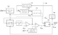
PSR(10)은 스위칭 파워 공급(1000)의 1 차측(11)에 배치되고, 스위칭 파워 공급(1000)은 출력 전압(Vo), 출력 전류(Io) 및 입력 전압(Vin)을 가진다.The
변압기(100)는 보조 권취(NA), 1 차측 권취(NP) 및 2 차측 권취(NS)를 포함함한다. 1 차측(11)은 입력 전압(Vin)의 접지 단자에서 공통적으로 접지되면서, 2 차측(22)은 출력 전압(Vo)의 접지 단자에서 공통적으로 접지된다.
PSR(10)은 전원 공급 단자(VDD), 접지 단자(GND), 출력 단자(VOUT), 방전 시간 검출 단자(VDET) 및 스위칭 전류 감지 단자(VS)를 가진다. PSR(10)은 방전 시간 검출 단자(VDET)를 통한 반사 전압(reflected voltage)(VW), 스위칭 전류 감지 단자(VS)를 통한, 1 차측 스위칭 전류(Ip)에 대응하는 1 차측 스위칭 전류 신호(Vcs)를 검출할 수 있고, 이에 따라서, 펄스 폭 변조 신호(VPWM)를 출력한다.The
펄스 폭 변조 신호(VPWM)는 출력 단자(VOUT)를 통하여 트랜지스터(SW)의 게이트에 연결된다. 따라서, PSR(10)은 펄스 폭 변조 신호(VPWM)를 통하여 트랜지스터(SW)를 스위칭할 수 있어서, 파워를 1 차측(11)에 입력하거나 또는 입력하지 않도록 제어할 수 있다. 1 차측 스위칭 전류 신호(VCS)는 자화 전류 신호(magnetizing current signal)일 수 있다. 반사 전압(VW)은 정류기(DDD)를 통하여 캐패시터(CDD)를 충전할 수 있고, 에너지를 PSR(10)에 제공한다.The pulse width modulation signal VPWM is connected to the gate of the transistor SW through the output terminal VOUT. Accordingly, the
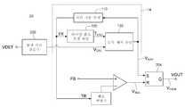
도 3a는 본 발명의 일 실시예에 따른 PSR의 회로 블럭도이다. PSR(10)은 펄스 폭 변조 신호 발생 회로(12) 및 동기 타이밍 펄스 발생 회로(14)를 포함한다. 펄스 폭 변조 신호 발생 회로(12)의 2 개의 입력 단자들은 방전 시간 검출 단자(VDET) 및 PSR(10)의 스위칭 전류 감지 단자(VS) 각각에 연결된다. 도 2a 및 3a를 참조하면, 반사 전압(VW)은 방전 시간 검출 단자(VDET)를 통하여 검출될 수 있고, 반사 전압(VW)은 2 차측 스위칭 전류(Is)에 응답한다. 반사 전압(VW)은, 2 차측 스위칭 전류(Is)가 0으로 떨어질 시에 급격하게 떨어질 것이다. 이로써, 펄스 폭 변조 신호 발생 회로(12)는 방전 시간 검출 단자(VDET)에 연결된 방전 시간 검출기(202)를 통하여 반사 전압(VW)을 검출할 수 있고, 이에 따라서, 2 차측 스위칭 전류(Is)에 대응하는 방전 시간 신호(VDSC)를 출력할 수 있다.3A is a circuit block diagram of a PSR according to an embodiment of the present invention. The
변압기(100)에 저장된 에너지가 2 차측(22)으로 방출될 시에, 방전 시간 신호(VDSC)는 하이 레벨(high level)에 있게 된다. 변압기(100)에 저장된 에너지의 방출이 달성되면(즉, 2 차측 스위칭 전류(Is)가 0으로 떨어짐), 방전 시간 신호(VDSC)는 로우 레벨에 있게 된다.When the energy stored in the
도 3a에 도시된 바와 같이, 펄스 폭 변조 신호 발생 회로(12)는, 출력 파형 재형성 회로, 필터, 증폭기 및 비교기의 신호 처리를 방전 시간 신호(VDSC), 1 차측 스위칭 전류 신호(VCS) 및 임계 전압(Vref2)에 관해 실행된 후에, 우선적으로 조정 신호(VMod)를 출력한다. 그 후, 또한 동기 타이밍 펄스 발생 회로(14)로부터의 시작 펄스(Vsync)에 따라서, 펄스 폭 변조 신호(VPWM)는 SR 플립-플롭(flip-flop)(204)을 통하여 출력된다. 예로서, 도 3b를 보면, 시작 펄스(Vsync)는, 펄스 폭 변조 신호(VPWM)가 하이 레벨로 스위칭될 시를 판별하기 위해 사용되면서, 조정 신호(VMod)는, 펄스 폭 변조 신호(VPWM)가 로우 레벨로 스위칭 될 시를 판별하기 위해 사용된다.As shown in FIG. 3A, the pulse width modulation
동기 타이밍 펄스 발생 회로(14)는 펄스 폭 변조 신호(VPWM)의 시작 펄스(Vsync)를 출력하기 위해 사용되고, 동기 타이밍 펄스 발생 회로(14)는 시간 지연 유닛(110), 타이밍 펄스 조정 유닛(120) 및 동기 제어 유닛(130)을 포함한다. 시간 지연 유닛(110)은 시작 펄스(Vsync)를 수신하고, 소정의 시간 동안 시작 펄스(Vsync)를 지연시킨 후에 제어 신호(TR)를 출력한다. 소정의 시간 구간은 특정 회로 사양에 따라 설계될 수 있다. 예를 들면, 소정의 시간은 50 ns 내지 100 ns일 수 있거나, 또는 SR 플립-플롭(204)의 유지 시간(hold time)보다 크도록 설정될 수 있다.The synchronous timing
타이밍 펄스 조정 유닛(120)은 제어 신호(TR)에 따른 타이밍 펄스 신호(TEND)를 출력한다. 도 4는 본 발명의 실시예에 따른 타이밍 펄스 조정 유닛의 내부 회로 배치도이다. 타이밍 펄스 조정 유닛(120)은 충전 및 방전 회로(300) 및 비교기(310)를 포함한다. 충전 및 방전 회로(300)는 캐패시터(302), 스위치 소자(304), 레벨 제한 회로(306) 및 일정한 전류원(320)을 포함한다.The timing
제어 신호(TR)는 스위치 소자(304)의 ON 또는 OFF를 제어하기 위해 사용될 수 있다. 예를 들면, 제어 신호(TR)가 로우 레벨에 있고, 스위치 소자(304)를 턴 오프하면, 회로(300)는 전원(VCC)에 연결된 일정한 전류원(320)을 통하여 캐패시터(302)를 충전할 수 있다. 제어 신호(TR)가 하이 레벨에 있는 반면(스위치 소자(304)는 ON), 캐패시터(302)는 접지에 연결된 스위치 소자(304)를 통하여 방전될 수 있다. 레벨 제한 회로(306)는, 충전 처리를 한 후의 하이 레벨 전압 값(VH)으로 전압 신호를, 방전 처리를 한 후의 로우 레벨 전압 값(VL)으로 전압 신호를, 각각 제한할 수 있고(즉, 전압 신호의 레벨 값은 최고 전압 값(VH)과 최저 전압 값(VL) 사이에서 제한된다), 이에 따라서 표시 신호(Vtri)를 출력할 수 있다. 표시 신호(Vtri)의 타이밍 파형도는 도 5a로서 도시되고, 레벨 제한 회로(306)는 도 4에 도시된 것으로 제한되지 않고, 이때, 도 4에서는 하이 레벨 전압값(VH) 및 로우 레벨 전압값(VL)이 연속적으로(back-to-back) 연결된 2 개의 다이오드들에 의해 제한된다.The control signal TR can be used to control the ON or OFF of the
표시 신호(Vtri)를 수신한 후에, 비교기(310)는 표시 신호(Vtri)를 기준 전압(reference voltage)(Vref1)과 비교하고, 이에 따라서, 타이밍 펄스 신호(TEND)를 출력한다. 하이 레벨 전압값(VH), 로우 레벨 전압값(VL) 및 기준 전압(Vref1)은 실제적인 회로 사양에 따라서 자가 작동 방식으로(self actuated way) 설계될 수도 있다. 도 5a 및 5b는 표시 신호(Vtri) 및 타이밍 펄스 신호(TEND)의 상대적인 타이밍 파형도이고, 여기서는 하이 레벨 전압값(VH)이 기준 전압(Vref1)보다 큰 실시예의 동작을 도시한다. 그러나, 기준 전압(Vref1) 및 하이 레벨 전압값(VH)은 사용자의 프리셋팅(presetting)에 따라서 동일할 수도 있고, 이는 본 발명의 권리 범위를 한정하기 위해 사용되지는 않는다.After receiving the display signal Vtri , the
도 6a는 본 발명의 실시예에 따른 동기 제어 유닛의 기능 블럭도이다. 동기 제어 유닛(130)은 인버터(502) 및 AND 논리 게이트(504)를 포함한다. 인버터(502)는 방전 시간 신호(VDSC)를 수신하고, 방전 시간 신호(VDSC)를 인버팅한 후에 역 방전 시간 신호(V'DSC)를 출력한다. AND 논리 게이트(504)의 2 개의 입력 단자들은 역 방전 시간 신호(V'DSC) 및 타이밍 펄스 신호(TEND)를 각각 수신하고, 이에 따라서, 시작 펄스(Vsync)를 출력한다. 방전 시간 신호(VDSC), 역 방전 시간 신호(V'DSC), 타이밍 펄스 신호(TEND) 및 시작 펄스(Vsync)의 상대적인 타이밍 파형도는 도 5b 내지 5e에서 도시된다.6A is a functional block diagram of a synchronous control unit according to an embodiment of the present invention. The
따라서, 다른 말로 하면, 역 방전 시간 신호(V'DSC) 및 타이밍 펄스 신호(TEND) 모두가 하이 레벨에 있게 될 시에만, AND 논리 게이트(504)는 시작 펄스(Vsync)를 하이 레벨로 인에이블시킬 수 있다(enable). 따라서, 시작 펄스(Vsync)의 트리거링 시간은 타이밍 펄스 신호(TEND) 또는 역 방전 시간 신호(V'DSC)로 동기화될 수 있다.Thus, in other words, the AND
특히, 예로서, 제 1 구간(T1)을 보면, 타이밍 펄스 신호(TEND)의 상승 에지(RT1)가 역 방전 시간 신호(V'DSC)의 상승 에지(RV1)보다 늦게 일어나면, 시작 펄스(Vsync)의 트리거링 시간은 타이밍 펄스 신호(TEND)의 상승 에지(RT1)로 동기화된다(즉, 나중의 에지). 제 2 구간(T2)에 대해, 타이밍 펄스 신호(TEND)의 상승 에지(RT2)가 역 방전 시간 신호(V'DSC)의 상승 에지(RV2)보다 일찍 일어날 시에도, 시작 펄스(Vsync)의 트리거링 시간은 역 방전 시간 신호(V'DSC)의 상승 에지(RV2)로 동기화된다(즉, 이 역시 나중의 에지). 상기에서 알 수 있는 바와 같이, 본 발명의 일 실시예에 따른 동기 제어 유닛(130)에서, 시작 펄스(Vsync)의 트리거링 시간은, 동일한 구간에서, 타이밍 펄스 신호(TEND)의 상승 에지 및 역 방전 시간 신호(V'DSC)의 상승 에지(즉, 방전 시간 신호(VDSC)의 하강 에지) 중 나중에 일어나는 상승 에지로 선택적으로 동기화될 수 있다.In particular, as an example, looking at the first section T1 , if the rising edge RT1 of the timing pulse signal TEND occurs later than the rising edge RV1 of the reverse discharge time signal V ′DSC , The triggering time of the start pulse Vsync is synchronized to the rising edge RT1 of the timing pulse signal TEND (ie, the later edge). For the second section T2 , even when the rising edge RT2 of the timing pulse signal TEND occurs earlier than the rising edge RV2 of the reverse discharge time signal V ′DSC , the start pulse ( The triggering time of Vsync is synchronized to the rising edge RV2 of the reverse discharge time signal V ′DSC (ie, this also a later edge). As can be seen above, in the
상기에서 보면, 시작 펄스(Vsync)는 펄스 폭 변조 신호(VPWM)의 펄스 시작 시간을 판별하기 위해 사용되어서(즉, 펄스 폭 변조 신호(VPWM)가 하이 레벨로 스위치되는 시간), 도 5f에 도시된 바와 같이, 펄스 폭 변조 신호(VPWM)의 펄스 시작 시간도, 동일한 구간에서, 타이밍 펄스 신호(TEND)의 상승 에지 및 역 방전 시간 신호(V'DSC)의 상승 에지 중 나중에 일어나는 상승 에지로 동기화될 수 있고, 이로 인해, 펄스 폭 변조 신호(VPWM)의 펄스 시작 시간을 조정하는 목적은 달성된다.From the above, a start pulse (Vsync) pulse width be used to determine the pulse start time of the modulated signal (VPWM) (i.e., time the pulse width modulated signal (VPWM), which switches to the high level), Fig. As shown in 5f, the pulse start time of the pulse width modulation signal VPWM is also equal to the later of the rising edge of the timing pulse signal TEND and the rising edge of the reverse discharge time signal V 'DSC in the same section. It can be synchronized to the rising edge which occurs, whereby the object of adjusting the pulse start time of the pulse width modulated signal VPWM is achieved.
도 2a를 참조하면, 펄스 폭 변조 신호(VPWM)의 하이 레벨 및 로우 레벨은 트랜지스터(SW)를 스위치하기 위해 사용되어, 파워를 1 차측(11)으로 입력하거나, 또는 입력하지 않도록 제어된다(즉, 1 차측 스위칭 전류(Ip)를 발생시키거나 발생시키지 않음). 따라서, 도 5c, 5f 및 5g를 참조하면, 제 1 구간(T1) 동안, 방전 시간 신호(VDSC)가 로우 레벨로 되돌아 갈 경우에도(즉, 2 차측 스위칭 전류(Is)가 0 지점으로 되돌아 감), 1 차측 스위칭 전류(Ip)는, 펄스 폭 변조 신호(VPWM)가 트리거되기 바로 전까지 형성되지 않아서, 1 차측 스위칭 전류(Ip)의 DCM(Discontinuous Conduction Mode)은 형성된다.Referring to FIG. 2A, the high level and low level of the pulse width modulated signal VPWM are used to switch the transistor SW so that the power is inputted to the
다음으로, 본 발명의 실시예에 따라서, 도 5a 내지 5g를 참조하면, 제 2 구간(T2) 후에, 펄스 폭 변조 신호(VPWM)의 펄스 시작 시간(즉, 시작 펄스(Vsync)의 트리거링 지점)은 방전 시간 신호(VDSC)의 하강 에지(즉, 역 방전 시간 신호(V'DSC)의 상승 에지)로 동기화되도록 조정된다. 따라서, 2 차측에서의 방전이 이루어진 후에, 스위칭 파워 공급은 (1 차측 스위칭 전류(Ip)를 형성하기 위해) 1 차측에서 충전되도록 효과적으로, 그리고 즉각적으로 다시 스위치되어, BCM(Boundary Conduction Mode)을 형성하고, 1 차측 권취(NP)를 통하여 나가는 인덕터 전류가 CCM에 들어가지 못하도록 할 수 있다.Next, according to an embodiment of the present invention, referring to FIGS. 5A to 5G, after the second interval T2 , the pulse start time (that is, the start pulse Vsync ) of the pulse width modulation signal VPWM is determined. The triggering point) is adjusted to synchronize to the falling edge of the discharge time signal VDSC (ie, the rising edge of the reverse discharge time signal V ′DSC ). Therefore, after the discharge on the secondary side has been made, the switching power supply is effectively and immediately switched back to charge on the primary side (to form the primary side switching current Ip), thereby forming a boundary conduction mode (BCM). In addition, it is possible to prevent the inductor current exiting through the primary winding NP from entering the CCM.
다음으로, 도 2a 및 3c를 참조하면, 도 3c는 본 발명의 또 다른 실시예에 따른 PSR의 회로 블럭도이다. 방전 시간 검출 단자(VDET)는 또한 밸리 검출기(valley detector)(206)에 연결될 수 있고, 밸리 검출기(206)는 방전 시간 검출 단자(VDET)를 통하여 반사 전압(VW)을 검출할 수 있고, 이에 따라서, 밸리 신호(VVLY)를 출력할 수 있어서, 트랜지스터(SW)의 간격을 턴-오프하는 동안 공진(resonance)의 최저점을 판별할 수 있다. 그러므로, 동기 타이밍 펄스 발생 회로(14)는 밸리 신호(VVLY) 및 시작 펄스(Vsync)에 따른 시간 지연, 타이밍 펄스 조정 및 동기 제어의 신호 처리를 실행할 수 있어서, 펄스 폭 변조 신호(VPWM)의 펄스 시작 시간(즉, 시작 펄스(Vsync))을 조정할 수 있다. 밸리 검출기(206)는 본 발명의 실시예에 따라서, 동기 타이밍 펄스 발생 회로(14)에 적용되어서, 시작 펄스(Vsync)를 조정하는 목적을 달성할 뿐만 아니라, 트랜지스터(SW)의 스위칭 손실도 줄이고(즉, 트랜지스터(SW)는 그의 밸리에서만 처리되도록 제한되고, 이로 인해, 그의 최고 주파수도 제한됨), 컨버터의 EMI(electromagnetic interference)를 줄일 수 있다.Next, referring to FIGS. 2A and 3C, FIG. 3C is a circuit block diagram of a PSR according to another embodiment of the present invention. The discharge time detection terminal VDET may also be connected to a
도 6b는 본 발명의 제 2 실시예에 따라서, 동기 제어 유닛의 내부 회로 배치도이다. 인버터(502) 및 AND 논리 게이트(504) 이외에, 동기 제어 유닛(130a)은 원 샷 회로(one shot circuit)(506), SR 플립-플롭(508) 및 시간 지연 유닛(510)을 더 포함할 수 있다.6B is an internal circuit layout diagram of a synchronous control unit, according to the second embodiment of the present invention. In addition to the
원 샷 회로(506)는 타이밍 펄스 신호(TEND)를 수신하고, 이에 따라서, 원 샷 타이밍 펄스 신호(VOS)를 얻기 위해 상기 수신된 타이밍 펄스 신호(TEND)를 전환한다. SR 플립-플롭(508)의 2 개의 입력 단자들은 원 샷 회로(506)의 출력 단자 및 시간 지연 유닛(510) 각각에 연결된다. 시간 지연 유닛(510)은 소정의 시간 동안 시작 펄스(Vsync)를 지연시키고, 그 후에, 상기 지연된 신호를 SR 플립-플롭(508)으로 출력한다. 따라서, SR 플립-플롭(508)은 원 샷 타이밍 펄스 신호(VOS) 및 소정의 시간 동안 지연된 후의 시작 펄스(Vsync)를 수신하고, 이에 따라서, 타이밍 펄스 신호(TEND)를 발생시켜서, 그 후에 AND 논리 게이트(504)가 시작 펄스(Vsync)를 출력하도록 한다.A one-
다음으로, 도 7은 본 발명의 제 3 실시예에 따른 동기 타이밍 펄스 발생 회로의 회로 블럭도이다. 동기 타이밍 펄스 발생 회로(14a)의 시간 지연 유닛(110)에 의해 수신된 시작 펄스(Vsync)는 원 샷 회로(140)에 의해 처리된 펄스 폭 변조 신호(VPWM) 후에 발생될 수도 있다. 즉, 시간 지연 유닛(110)이 전기적으로 다른 외부 회로들에 연결되는 실제적인 연결 방식은 본 발명의 권리 범위를 한정시키기 위해 사용되지는 않는다. 본 발명의 실시예에 따른 경우들에서, 시간 지연 유닛(110)은 타이밍 펄스 조정 유닛(120) 및 동기 제어 유닛(130)이 다음 신호 처리를 실행하도록 펄스 폭 변조 신호(VPWM)의 시작 펄스(Vsync)를 수신하여, 본 발명의 일반성을 저하시킴 없이, 동일한 구간에서, 시작 펄스(Vsync)가 타이밍 펄스 신호(TEND) 또는 역 방전 시간 신호(V'DSC) 중 나중에 일어나는 상승 에지로 동기화되도록 할 수 있다.Next, Fig. 7 is a circuit block diagram of a synchronous timing pulse generation circuit according to the third embodiment of the present invention. The start pulse Vsync received by the
도 8a는 본 발명의 제 4 실시예에 따라서, 동기 타이밍 펄스 발생 회로(14)를 포함하는 전압 모드 제어(PSR)의 적용 구조물의 회로 블럭도이다. 도 8b 및 8c는 본 발명의 제 5 실시예 및 제 6 실시예에 따라서 동기 타이밍 펄스 발생 회로(14)를 각각 포함하는 전압 모드 제어(SSR) 및 전류 모드 제어(SSR)의 회로 블럭도이다. 이로써, 본 발명의 실시예에 따른 동기 타이밍 펄스 발생 회로는 일정한 전압 모드 또는 일정한 전류 모드에 한정됨 없이, PSR 또는 SSR에 선택적으로 배치될 수 있다.8A is a circuit block diagram of an application structure of voltage mode control (PSR) including a synchronous timing
다음으로, 본 발명의 실시예에 따른 동기 타이밍 펄스 발생 회로는, 조정될 수 있는 펄스 시작 시간을 가진 펄스 폭 변조 신호를 더 제어하고 출력하기 위해서, 스위칭 파워 공급의 회로 조정기에 적용되고, 이로 인해, 스위칭 파워 공급의 인덕터 전류는 CCM에 들어가지 못한다.Next, a synchronous timing pulse generation circuit according to an embodiment of the present invention is applied to a circuit regulator of switching power supply, in order to further control and output a pulse width modulated signal having an adjustable pulse start time. The inductor current of the switching power supply does not enter the CCM.
Claims (11)
Translated fromKorean상기 스위칭 파워 공급은 1 차측 및 2 차측을 가지고,
상기 스위칭 파워 공급은 펄스 폭 변조 신호를 통하여 상기 1 차측에 파워가 선택적으로 입력될 수 있거나 또는 입력될 수 없도록 하고,
상기 동기 타이밍 펄스 발생 회로는 상기 펄스 폭 변조 신호의 시작 펄스를 발생시키기 위해 사용되고,
상기 동기 타이밍 펄스 발생 회로는, 상기 시작 펄스를 소정의 시간 동안 지연시킨 후에 제어 신호를 출력하는 시간 지연 유닛; 일정한 전류원이 상기 제어 신호에 따라서 타이밍 펄스 조정 유닛을 선택적으로 충전시킬 수 있도록 하고, 이에 따라서 타이밍 펄스 신호를 출력하는 타이밍 펄스 조정 유닛; 및 상기 2 차측의 방전 시간 신호 및 상기 타이밍 펄스 신호에 따라서 상기 시작 펄스를 출력하는 동기 제어 유닛을 포함하고,
상기 타이밍 펄스 신호는 상승 에지를 가지고, 상기 방전 시간 신호는 하강 에지를 가지고,
상기 시작 펄스의 트리거링 시간은, 동일한 구간에서, 상기 타이밍 펄스 신호의 상승 에지 및 상기 방전 시간 신호의 하강 에지 중 나중에 일어나는 에지로 동기화되고,
상기 시작 펄스는 상기 펄스 폭 변조 신호의 펄스 시작 시간을 판별하기 위해 사용되는 것을 특징으로 하는 동기 타이밍 펄스 발생 회로.A synchronous timing pulse generation circuit applicable to a switching power supply,
The switching power supply has a primary side and a secondary side,
The switching power supply may or may not be selectively input to the primary side via a pulse width modulated signal,
The synchronous timing pulse generation circuit is used to generate a start pulse of the pulse width modulated signal,
The synchronous timing pulse generating circuit includes: a time delay unit for outputting a control signal after delaying the start pulse for a predetermined time; A timing pulse adjustment unit which enables a constant current source to selectively charge the timing pulse adjustment unit in accordance with the control signal, and outputs a timing pulse signal accordingly; And a synchronous control unit for outputting the start pulse in accordance with the discharge time signal on the secondary side and the timing pulse signal,
The timing pulse signal has a rising edge, the discharge time signal has a falling edge,
The triggering time of the start pulse is synchronized to an edge which occurs later of the rising edge of the timing pulse signal and the falling edge of the discharge time signal in the same interval,
The start pulse is used to determine a pulse start time of the pulse width modulated signal.
상기 타이밍 펄스 조정 유닛은:
상기 제어 신호 및 상기 일정한 전류원에 따라서 표시 신호를 출력하는 충전 및 방전 회로; 및
상기 표시 신호를 기준 전압과 비교하고, 이에 따라서 상기 타이밍 펄스 신호를 출력하는 비교기를 포함하는 것을 특징으로 하는 동기 타이밍 펄스 발생 회로.The method of claim 1,
The timing pulse adjustment unit is:
A charging and discharging circuit outputting a display signal in accordance with the control signal and the constant current source; And
And a comparator for comparing the display signal with a reference voltage and outputting the timing pulse signal accordingly.
상기 충전 및 방전 회로는:
상기 일정한 전류원과 접지 사이에 연결된 캐패시터;
상기 캐패시터와 상기 접지 사이에 전기적으로 연결된 스위치 소자(상기 스위치 소자의 ON 또는 OFF는 상기 제어 신호에 의해 제어되어, 상기 일정한 전류원이 상기 캐패시터를 충전할지를 제어함); 및
상기 표시 신호를 출력하기 위해, 상기 캐패시터에 의해 출력된 신호의 레벨을 제한하는 레벨 제한 회로를 포함하는 것을 특징으로 하는 동기 타이밍 펄스 발생 회로.The method of claim 2,
The charge and discharge circuit is:
A capacitor coupled between the constant current source and ground;
A switch element electrically connected between the capacitor and the ground (ON or OFF of the switch element is controlled by the control signal to control whether the constant current source charges the capacitor); And
And a level limiting circuit for limiting the level of the signal output by the capacitor to output the display signal.
상기 동기 제어 유닛은:
상기 방전 시간 신호를 수신하고, 역 방전 시간 신호를 출력하는 인버터; 및
상기 타이밍 펄스 신호 및 상기 역 방전 시간 신호를 수신하고, 이에 따라서 상기 시작 펄스를 출력하는 AND 논리 게이트를 포함하는 것을 특징으로 하는 동기 타이밍 펄스 발생 회로.The method of claim 1,
The synchronous control unit is:
An inverter configured to receive the discharge time signal and output a reverse discharge time signal; And
And an AND logic gate which receives the timing pulse signal and the reverse discharge time signal and accordingly outputs the start pulse.
상기 동기 제어 유닛은:
상기 타이밍 펄스 신호를 수신하고, 원 샷 타이밍 펄스 신호를 출력하는 원 샷 회로;
상기 시작 펄스를 소정의 시간 동안 지연시킨 후에 상기 제어 신호를 출력하는 시간 지연 유닛; 및
상기 원 샷 타이밍 펄스 신호 및 상기 제어 신호를 수신하고, 이에 따라서 상기 타이밍 펄스 신호를 출력하는 플립-플롭을 더 포함하는 것을 특징으로 하는 동기 타이밍 펄스 발생 회로.The method of claim 4, wherein
The synchronous control unit is:
A one shot circuit which receives the timing pulse signal and outputs a one shot timing pulse signal;
A time delay unit for outputting the control signal after delaying the start pulse for a predetermined time; And
And a flip-flop which receives the one shot timing pulse signal and the control signal and accordingly outputs the timing pulse signal.
상기 스위칭 파워 공급은 1 차측 및 2 차측을 가지고,
상기 스위칭 파워 공급은 펄스 폭 변조 신호를 통하여 상기 1 차측에 파워가 선택적으로 입력될 수 있거나 또는 입력될 수 없도록 하고,
상기 회로 조정기는: 상기 1 차측의 1 차측 스위칭 전류 신호 및 상기 2 차측의 방전 시간 신호에 따라서, 시작 펄스를 가진 펄스 폭 변조 신호를 출력하는 펄스 폭 변조 신호 발생 회로; 및 시간 지연, 타이밍 펄스 조정 및 동기 제어의 신호 처리를 상기 펄스 폭 변조 신호 및 상기 방전 시간 신호에 관해 실행한 후에, 상기 시작 펄스를 출력하는 동기 타이밍 펄스 발생 회로를 포함하고, 이때, 상기 시작 펄스는 상기 펄스 폭 변조 신호의 펄스 시작 시간을 판별하기 위해 사용되는 것을 특징으로 하는 회로 조정기.In a circuit regulator applicable to a switching power supply,
The switching power supply has a primary side and a secondary side,
The switching power supply may or may not be selectively input to the primary side via a pulse width modulated signal,
The circuit regulator comprises: a pulse width modulated signal generating circuit for outputting a pulse width modulated signal having a start pulse in accordance with the primary side switching current signal on the primary side and the discharge time signal on the secondary side; And a synchronous timing pulse generating circuit for outputting the start pulse after performing signal processing of time delay, timing pulse adjustment, and synchronous control on the pulse width modulation signal and the discharge time signal, wherein the start pulse Is used to determine a pulse start time of the pulse width modulated signal.
상기 동기 타이밍 펄스 발생 회로는:
상기 시작 펄스를 수신하고, 상기 시작 펄스를 소정의 시간 동안 지연시킨 후에 제어 신호를 출력하는 시간 지연 유닛;
일정한 전류원이 상기 제어 신호에 따라서 타이밍 펄스 조정 유닛을 선택적으로 충전시킬 수 있도록 하고, 이에 따라서 타이밍 펄스 신호를 출력하는 타이밍 펄스 조정 유닛; 및
상기 방전 시간 신호 및 상기 타이밍 펄스 신호에 따라서 상기 시작 펄스를 출력하는 동기 제어 유닛
을 포함하고,
상기 타이밍 펄스 신호는 상승 에지를 가지고, 상기 방전 시간 신호는 하강 에지를 가지고, 상기 시작 펄스의 트리거링 시간은, 동일한 구간에서, 상기 타이밍 펄스 신호의 상승 에지 및 상기 방전 시간 신호의 하강 에지 중 나중에 일어나는 에지로 동기화되는 것을 특징으로 하는 회로 조정기.The method according to claim 6,
The synchronous timing pulse generation circuit is:
A time delay unit for receiving the start pulse and outputting a control signal after delaying the start pulse for a predetermined time;
A timing pulse adjustment unit which enables a constant current source to selectively charge the timing pulse adjustment unit in accordance with the control signal, and outputs a timing pulse signal accordingly; And
A synchronous control unit for outputting the start pulse in accordance with the discharge time signal and the timing pulse signal
Including,
The timing pulse signal has a rising edge, the discharge time signal has a falling edge, and the triggering time of the start pulse occurs in the same interval, one of a rising edge of the timing pulse signal and a falling edge of the discharge time signal later. Circuit regulator, characterized in that the edge is synchronized.
상기 타이밍 펄스 조정 유닛은:
상기 제어 신호 및 상기 일정한 전류원에 따라서 표시 신호를 출력하는 충전 및 방전 회로; 및
상기 표시 신호를 기준 전압과 비교하고, 이에 따라서 상기 타이밍 펄스 신호를 출력하는 비교기를 포함하는 것을 특징으로 하는 회로 조정기.The method of claim 7, wherein
The timing pulse adjustment unit is:
A charging and discharging circuit outputting a display signal in accordance with the control signal and the constant current source; And
And a comparator for comparing said display signal with a reference voltage and thereby outputting said timing pulse signal.
상기 충전 및 방전 회로는:
상기 일정한 전류원과 접지 사이에 연결된 캐패시터;
상기 캐패시터와 상기 접지 사이에 전기적으로 연결된 스위치 소자(상기 스위치 소자의 ON 또는 OFF는 상기 제어 신호에 의해 제어되어, 상기 일정한 전류원이 상기 캐패시터를 충전할지를 제어함); 및
상기 표시 신호를 출력하기 위해, 상기 캐패시터에 의해 출력된 신호의 레벨을 제한하는 레벨 제한 회로를 포함하는 것을 특징으로 하는 회로 조정기.The method of claim 8,
The charge and discharge circuit is:
A capacitor coupled between the constant current source and ground;
A switch element electrically connected between the capacitor and the ground (ON or OFF of the switch element is controlled by the control signal to control whether the constant current source charges the capacitor); And
And a level limiting circuit for limiting the level of the signal output by the capacitor to output the display signal.
상기 동기 제어 유닛은:
상기 방전 시간 신호를 수신하고, 역 방전 시간 신호를 출력하는 인버터; 및
상기 타이밍 펄스 신호 및 상기 역 방전 시간 신호를 수신하고, 이에 따라서 상기 시작 펄스를 출력하는 AND 논리 게이트를 포함하는 것을 특징으로 하는 회로 조정기.The method of claim 7, wherein
The synchronous control unit is:
An inverter configured to receive the discharge time signal and output a reverse discharge time signal; And
And an AND logic gate that receives the timing pulse signal and the reverse discharge time signal and accordingly outputs the start pulse.
상기 동기 제어 유닛은:
상기 타이밍 펄스 신호를 수신하고, 원 샷 타이밍 펄스 신호를 출력하는 원 샷 회로;
상기 시작 펄스를 소정의 시간 동안 지연시킨 후에 상기 제어 신호를 출력하는 시간 지연 유닛; 및
상기 원 샷 타이밍 펄스 신호 및 상기 제어 신호를 수신하고, 이에 따라서 상기 타이밍 펄스 신호를 출력하는 플립-플롭을 더 포함하는 것을 특징으로 하는 회로 조정기.The method of claim 10,
The synchronous control unit is:
A one shot circuit which receives the timing pulse signal and outputs a one shot timing pulse signal;
A time delay unit for outputting the control signal after delaying the start pulse for a predetermined time; And
And a flip-flop which receives the one shot timing pulse signal and the control signal and accordingly outputs the timing pulse signal.
Applications Claiming Priority (2)
| Application Number | Priority Date | Filing Date | Title |
|---|---|---|---|
| TW099125990 | 2010-08-04 | ||
| TW099125990ATWI419469B (en) | 2010-08-04 | 2010-08-04 | Regulator and synchronized pulse generator thereof |
Publications (2)
| Publication Number | Publication Date |
|---|---|
| KR20120013174A KR20120013174A (en) | 2012-02-14 |
| KR101121300B1true KR101121300B1 (en) | 2012-03-20 |
Family
ID=45002186
Family Applications (1)
| Application Number | Title | Priority Date | Filing Date |
|---|---|---|---|
| KR1020100133814AActiveKR101121300B1 (en) | 2010-08-04 | 2010-12-23 | Circuit regulator and synchronous timing pulse generation circuit thereof |
Country Status (6)
| Country | Link |
|---|---|
| US (1) | US8422253B2 (en) |
| EP (1) | EP2416474B1 (en) |
| JP (1) | JP5181014B2 (en) |
| KR (1) | KR101121300B1 (en) |
| ES (1) | ES2661843T3 (en) |
| TW (1) | TWI419469B (en) |
Families Citing this family (16)
| Publication number | Priority date | Publication date | Assignee | Title |
|---|---|---|---|---|
| EP2445098B1 (en)* | 2010-10-25 | 2019-08-07 | STMicroelectronics Srl | Control device for a resonant converter. |
| MX2012013946A (en)* | 2011-12-01 | 2013-06-17 | Rab Lighting Inc | Led driver protection circuit. |
| TWI444102B (en)* | 2012-05-30 | 2014-07-01 | Macroblock Inc | Driving circuit for led |
| US8665612B2 (en)* | 2012-07-10 | 2014-03-04 | Immense Advance Technology Corporation | Constant current controller |
| JP5814876B2 (en) | 2012-07-27 | 2015-11-17 | 株式会社東芝 | Synchronous rectification type power supply circuit and adjustment method thereof |
| US9197124B2 (en)* | 2012-10-24 | 2015-11-24 | Marvell World Trade Ltd. | Method and apparatus to reduce overcurrent during the startup of a switching regulator |
| TWI488414B (en)* | 2012-10-30 | 2015-06-11 | Lite On Technology Corp | A flyback voltage converter with primary side feedback controlling and a voltage controlling method thereof |
| SG11201502947UA (en) | 2013-10-28 | 2015-06-29 | Advanced Charging Technologies Llc | Electrical circuit for powering consumer electronic devices |
| CN104702130B (en)* | 2013-12-05 | 2017-05-03 | 立锜科技股份有限公司 | Control circuit of power supply conversion circuit |
| US9762132B2 (en) | 2014-10-28 | 2017-09-12 | Advanced Charging Technologies, LLC | Electrical circuit for delivering power to consumer electronic devices |
| TWI575854B (en)* | 2015-01-08 | 2017-03-21 | 群光電能科技股份有限公司 | Speedydischarging circuit and power supply apparatus with speedydischarging circuit |
| CN109361500A (en)* | 2018-10-25 | 2019-02-19 | 南通先进通信技术研究院有限公司 | A method of the plesiochronous external pulse of self-correcting based on chip |
| EP3666735A1 (en)* | 2018-12-14 | 2020-06-17 | ABB Schweiz AG | Dielectric barrier discharge for ballast water treatment using optimized voltage shape control |
| CN111880038B (en)* | 2020-08-07 | 2022-04-01 | 广东电网有限责任公司 | Secondary circuit proofreading device |
| TWI740676B (en) | 2020-10-12 | 2021-09-21 | 財團法人工業技術研究院 | Pulse-width modulation signal observation circuit and hardware-in-the-loop simulation device having the same |
| US11962247B2 (en)* | 2021-02-25 | 2024-04-16 | Richtek Technology Corporation | Resonant half-bridge flyback power converter with skipping cycles and control method thereof |
Citations (1)
| Publication number | Priority date | Publication date | Assignee | Title |
|---|---|---|---|---|
| JP2009512406A (en) | 2005-10-09 | 2009-03-19 | システム ジェネラル コーポレーション | Switching control circuit with variable switching frequency for a power converter with controlled primary side |
Family Cites Families (13)
| Publication number | Priority date | Publication date | Assignee | Title |
|---|---|---|---|---|
| US4870555A (en)* | 1988-10-14 | 1989-09-26 | Compaq Computer Corporation | High-efficiency DC-to-DC power supply with synchronous rectification |
| US6650552B2 (en)* | 2001-05-25 | 2003-11-18 | Tdk Corporation | Switching power supply unit with series connected converter circuits |
| JP3488709B2 (en)* | 2001-12-12 | 2004-01-19 | 株式会社東芝 | Switching power supply |
| US6836415B1 (en)* | 2003-06-18 | 2004-12-28 | Systems General Corp. | Primary-side regulated pulse width modulation controller with improved load regulation |
| US6980441B2 (en)* | 2003-07-28 | 2005-12-27 | Astec International Limited | Circuit and method for controlling a synchronous rectifier in a power converter |
| GB2438464A (en)* | 2006-05-23 | 2007-11-28 | Cambridge Semiconductor Ltd | Regulating the output of a switch mode power supply |
| TWI314808B (en)* | 2006-09-06 | 2009-09-11 | Delta Electronics Inc | Resonance converter and driving method for synchronous rectifier thereof |
| US20080062725A1 (en)* | 2006-09-11 | 2008-03-13 | Ta-Yung Yang | Multi-channels power converter having power saving means to improve light load efficiency |
| JP4806333B2 (en)* | 2006-11-09 | 2011-11-02 | 本田技研工業株式会社 | DC-DC converter |
| JP2009071997A (en)* | 2007-09-13 | 2009-04-02 | Panasonic Electric Works Co Ltd | Power converter and vehicular lamp |
| US7983061B2 (en)* | 2008-02-22 | 2011-07-19 | System General Corporation | Switching controller capable of reducing acoustic noise for power converters |
| JP5165454B2 (en)* | 2008-05-14 | 2013-03-21 | 株式会社ダイヘン | Power supply |
| WO2010083511A1 (en)* | 2009-01-19 | 2010-07-22 | Flextronics International Usa, Inc. | Controller for a power converter |
- 2010
- 2010-08-04TWTW099125990Apatent/TWI419469B/enactive
- 2010-12-15EPEP10195113.5Apatent/EP2416474B1/enactiveActive
- 2010-12-15ESES10195113.5Tpatent/ES2661843T3/enactiveActive
- 2010-12-16USUS12/970,029patent/US8422253B2/enactiveActive
- 2010-12-17JPJP2010282090Apatent/JP5181014B2/enactiveActive
- 2010-12-23KRKR1020100133814Apatent/KR101121300B1/enactiveActive
Patent Citations (1)
| Publication number | Priority date | Publication date | Assignee | Title |
|---|---|---|---|---|
| JP2009512406A (en) | 2005-10-09 | 2009-03-19 | システム ジェネラル コーポレーション | Switching control circuit with variable switching frequency for a power converter with controlled primary side |
Also Published As
| Publication number | Publication date |
|---|---|
| JP2012039844A (en) | 2012-02-23 |
| JP5181014B2 (en) | 2013-04-10 |
| ES2661843T3 (en) | 2018-04-04 |
| EP2416474A2 (en) | 2012-02-08 |
| KR20120013174A (en) | 2012-02-14 |
| US20120033459A1 (en) | 2012-02-09 |
| TWI419469B (en) | 2013-12-11 |
| EP2416474A3 (en) | 2014-10-29 |
| US8422253B2 (en) | 2013-04-16 |
| TW201208259A (en) | 2012-02-16 |
| EP2416474B1 (en) | 2017-12-27 |
Similar Documents
| Publication | Publication Date | Title |
|---|---|---|
| KR101121300B1 (en) | Circuit regulator and synchronous timing pulse generation circuit thereof | |
| US11671020B2 (en) | Flyback converter, control circuit and control method thereof | |
| US11764684B2 (en) | Systems and methods for regulating power conversion systems with output detection and synchronized rectifying mechanisms | |
| JP6915115B2 (en) | How to Control Secondary Controllers, Power Converters, and Synchronous Flyback Converters for Use in Synchronous Flyback Converters | |
| US11588405B2 (en) | Systems and methods for regulating power conversion systems with output detection and synchronized rectifying mechanisms | |
| CN106059304B (en) | Switch with efficient voltage reduction using secondary switches | |
| TWI626824B (en) | System and method with timing control for synchronous rectification controller | |
| US9641082B2 (en) | Systems and methods for zero voltage switching in power conversion systems | |
| CN113489328B (en) | Zero-voltage switching control circuit, flyback power supply circuit and control method thereof | |
| JP6968638B2 (en) | Modulating the jitter frequency as the switching frequency approaches the jitter frequency | |
| US11201546B2 (en) | Power converter and control circuit thereof | |
| Wu et al. | Quasi-resonant flyback converter with new valley voltage detection mechanism | |
| CN102377414B (en) | Circuit regulator and its synchronous clock pulse generating circuit | |
| CN118232699A (en) | Enable circuit with winding signal detection | |
| JP2001119944A (en) | Direct current-to-direct current converter |
Legal Events
| Date | Code | Title | Description |
|---|---|---|---|
| A201 | Request for examination | ||
| PA0109 | Patent application | Patent event code:PA01091R01D Comment text:Patent Application Patent event date:20101223 | |
| PA0201 | Request for examination | ||
| E701 | Decision to grant or registration of patent right | ||
| PE0701 | Decision of registration | Patent event code:PE07011S01D Comment text:Decision to Grant Registration Patent event date:20111216 | |
| PG1501 | Laying open of application | ||
| GRNT | Written decision to grant | ||
| PR0701 | Registration of establishment | Comment text:Registration of Establishment Patent event date:20120221 Patent event code:PR07011E01D | |
| PR1002 | Payment of registration fee | Payment date:20120221 End annual number:3 Start annual number:1 | |
| PG1601 | Publication of registration | ||
| FPAY | Annual fee payment | Payment date:20150120 Year of fee payment:4 | |
| PR1001 | Payment of annual fee | Payment date:20150120 Start annual number:4 End annual number:4 | |
| FPAY | Annual fee payment | Payment date:20160119 Year of fee payment:5 | |
| PR1001 | Payment of annual fee | Payment date:20160119 Start annual number:5 End annual number:5 | |
| FPAY | Annual fee payment | Payment date:20170119 Year of fee payment:6 | |
| PR1001 | Payment of annual fee | Payment date:20170119 Start annual number:6 End annual number:6 | |
| FPAY | Annual fee payment | Payment date:20180118 Year of fee payment:7 | |
| PR1001 | Payment of annual fee | Payment date:20180118 Start annual number:7 End annual number:7 | |
| FPAY | Annual fee payment | Payment date:20190116 Year of fee payment:8 | |
| PR1001 | Payment of annual fee | Payment date:20190116 Start annual number:8 End annual number:8 | |
| FPAY | Annual fee payment | Payment date:20200115 Year of fee payment:9 | |
| PR1001 | Payment of annual fee | Payment date:20200115 Start annual number:9 End annual number:9 | |
| PR1001 | Payment of annual fee | Payment date:20210115 Start annual number:10 End annual number:10 | |
| PR1001 | Payment of annual fee | Payment date:20220118 Start annual number:11 End annual number:11 | |
| PR1001 | Payment of annual fee | Payment date:20230117 Start annual number:12 End annual number:12 | |
| PR1001 | Payment of annual fee | Payment date:20240109 Start annual number:13 End annual number:13 |