KR101120043B1 - Microstrip line-suspended stripline transition structure and application module thereof - Google Patents
Microstrip line-suspended stripline transition structure and application module thereofDownload PDFInfo
- Publication number
- KR101120043B1 KR101120043B1KR1020090132350AKR20090132350AKR101120043B1KR 101120043 B1KR101120043 B1KR 101120043B1KR 1020090132350 AKR1020090132350 AKR 1020090132350AKR 20090132350 AKR20090132350 AKR 20090132350AKR 101120043 B1KR101120043 B1KR 101120043B1
- Authority
- KR
- South Korea
- Prior art keywords
- line
- signal line
- ground
- suspended strip
- ssl
- Prior art date
- Legal status (The legal status is an assumption and is not a legal conclusion. Google has not performed a legal analysis and makes no representation as to the accuracy of the status listed.)
- Expired - Fee Related
Links
Images


Classifications
- H—ELECTRICITY
- H01—ELECTRIC ELEMENTS
- H01P—WAVEGUIDES; RESONATORS, LINES, OR OTHER DEVICES OF THE WAVEGUIDE TYPE
- H01P3/00—Waveguides; Transmission lines of the waveguide type
- H01P3/02—Waveguides; Transmission lines of the waveguide type with two longitudinal conductors
- H01P3/08—Microstrips; Strip lines
- H01P3/081—Microstriplines
- H—ELECTRICITY
- H01—ELECTRIC ELEMENTS
- H01P—WAVEGUIDES; RESONATORS, LINES, OR OTHER DEVICES OF THE WAVEGUIDE TYPE
- H01P1/00—Auxiliary devices
- H01P1/20—Frequency-selective devices, e.g. filters
- H01P1/213—Frequency-selective devices, e.g. filters combining or separating two or more different frequencies
Landscapes
- Control Of Motors That Do Not Use Commutators (AREA)
Abstract
Translated fromKoreanDescription
Translated fromKorean본 발명은 마이크로스트립 선로(MSL: Micorostrip line)와 서스펜디드 스트립선로(SSL: Suspended Stripline)간의 전이 구조에 관한 것으로서, 보다 상세하게는 마이크로스트립 선로에서 동일 평면 도파관(CPW: Coplanar Waveguide)으로, CPW에서 SSL로의 전이구조와 기판의 상하에 연결되는 하우징을 포함하는 구조로서, 이를 통해 Q 값(품질계수)이 향상되는 필터 및 다양한 응용 모듈을 구현할 수 있는 마이크로스트립 선로와 서스펜디드 스트립선로간 전이구조 및 그 응용 모듈에 관한 것이다.The present invention relates to a transition structure between a microstrip line (MSL: Micorostrip line) and a suspended strip line (SSL), and more particularly, to a coplanar waveguide (CPW) in a microstrip line. A structure including a transition structure to SSL and a housing connected to the upper and lower sides of the substrate, and the transition structure between the microstrip line and the suspended strip line to implement a filter and various application modules with improved Q value (quality factor), and Relates to an application module.
서스펜디드 스트립선로(SSL)는 일종의 스트립선로(stripline)의 수정된 형태라고 할 수 있다. 스트립선로는 유전체 기판의 중앙에 도체의 신호선로가 있고, 선로의 아래위에 위치한 금속판이 접지면으로 형성된 전송선로이다. 따라서 전자파는 신호선로를 중심으로 상하 대칭적으로 형성되고 유전체 내에서 전파하게 되므로, 도체에 의한 손실 및 유전체 손실이 발생하게 된다.Suspended strip line (SSL) is a modified form of a stripline (stripline). The strip line is a signal line of a conductor in the center of the dielectric substrate, and a transmission line in which a metal plate located above and below the line is formed as a ground plane. Therefore, since electromagnetic waves are symmetrically formed around the signal line and propagate in the dielectric, losses due to the conductor and dielectric loss occur.
한편, SSL은 금속의 캐비티(cavity) 중앙에 얇은 유전체 기판이 위치하고 있으며, 이러한 유전체 기판 양면의 도체를 이용하여 신호선로가 형성되고, 상하좌우에 위치한 금속면이 접지면으로 형성되는 전송선로이다.On the other hand, SSL is a thin dielectric substrate is located in the center of the cavity (cavity) of the metal, the signal line is formed by using the conductors on both sides of the dielectric substrate, the metal line located in the upper, lower, left and right is formed as the ground plane.
SSL의 매질은 거의 공기로 채워져 있어 유효 유전율이 1에 가까우며, 대부분의 전자파는 전송선로 상하의 공기를 통해 전파되므로 유전체에 의한 손실이 매우 적어지게 된다.Since the medium of SSL is almost filled with air, the effective dielectric constant is close to 1, and most electromagnetic waves propagate through the air above and below the transmission line, so that the loss caused by the dielectric is very small.
이런 SSL은 다음과 같은 장점을 가지고 있다.This SSL has the following advantages:
첫째, 대부분의 진행되는 전자파의 에너지가 공기 중으로 진행되므로 유전체 손실이 거의 없어 높은 Q 값을 가지게 된다.First, since most of the energy of the electromagnetic waves proceeds in the air, there is almost no dielectric loss, resulting in a high Q value.
둘째, 삽입 손실 및 군 지연 특성이 아주 우수하다.Second, insertion loss and group delay characteristics are very good.
셋째, 인쇄된 전송선과는 달리 차폐가 되어 있어, 외부로 방사되는 에너지가 거의 없다.Third, unlike printed transmission lines, they are shielded, so there is little energy radiated to the outside.
넷째, 다양한 임피던스를 구현할 수 있기 때문에 설계의 폭이 넓다.Fourth, the design is wide because various impedances can be realized.
다섯째, 강한 커플링의 커패시턴스 구현이 가능해 넓은 대역의 필터 제작이 용이하다.Fifth, it is possible to realize a large coupling capacitance, making it easy to manufacture a wide band filter.
반면, SSL은 다음과 같은 단점을 가지고 있다.On the other hand, SSL has the following disadvantages.
첫째, SSL의 구조상 소형화 하는 데에 어려움이 있다.First, there is a difficulty in miniaturizing the structure of SSL.
둘째, 하우징 제작에 있어서 정교한 기술이 요구된다.Secondly, sophisticated technology is required in housing manufacture.
셋째, 하우징의 필요로 인해 다른 전송선로와의 연결이 어렵기때문에 커넥터를 연결하여 하우징으로 구성된 단일 소자의 모듈로 구성되는 경우가 대부분이다.Third, since it is difficult to connect with other transmission lines due to the need of the housing, it is mostly composed of a single element module composed of a housing by connecting a connector.
한편, 마이크로스트립 선로는 상용으로 마이크로파 및 밀리미터파 신호를 전송하기 위해 가장 많이 쓰이는 선로이며, 이러한 마이크로스트립 선로 기반의 회로와 SSL을 사용하여 구현할 수 있는 높은 Q 값을 갖는 필터 혹은 응용 소자들을 쉽게 연결하기 위해서는 두 전송선로 사이의 전이구조가 필수적이다.Microstrip lines, on the other hand, are the most commonly used for commercially transmitting microwave and millimeter wave signals, and easily connect these microstrip line-based circuits with high Q-value filters or applications that can be implemented using SSL. In order to do this, the transition structure between two transmission lines is essential.
기존의 SSL을 이용한 필터 연구는 주로 커넥터를 직접 하우징에 부착하고, 커넥터의 동축 피드(feed)가 SSL의 선로에 접촉하는 전이구조를 이용한 것이 대부분이었다. 이 경우 커넥터의 피드와 기판의 접촉에 따른 기생 성분이 생성되기 때문에 SSL 필터의 튜닝이 불가피 하였다.The existing research on the filter using SSL is mainly using a transition structure in which the connector is directly attached to the housing and the coaxial feed of the connector contacts the SSL line. In this case, tuning of the SSL filter is inevitable because parasitic components are generated due to contact between the feed of the connector and the substrate.
또한 마이크로스트립 선로로부터 전이구조를 사용하여 SSL 필터를 구현한 기존의 연구를 살펴보면, 전이구조 자체가 필터의 일부분으로 즉, 커패시턴스 성분 혹은 인덕턴스 성분으로 되어, 필터의 해석에 있어 어려움이 있었다.In addition, the existing researches on the implementation of the SSL filter using the transition structure from the microstrip line show that the transition structure itself is a part of the filter, that is, the capacitance component or the inductance component.
상기와 같은 문제점을 해결하기 위하여 창안된 본 발명의 실시예에 따른 목적은, 다양한 마이크로스트립 선로 기반의 회로를 SSL과 편리하게 연결하여 사용할 수 있도록 마이크로스트립 선로와 SSL간 전이구조를 제공함으로써, 이를 통해 Q 값이 향상되는 필터 및 다양한 응용 모듈을 구현할 수 있는 마이크로스트립 선로와 서스펜디드 스트립선로간 전이구조 및 그 응용 모듈을 제공하는데 있다.An object according to an embodiment of the present invention was devised to solve the above problems, by providing a transition structure between the microstrip line and SSL so that various microstrip line-based circuits can be conveniently connected to the SSL, The present invention provides a transition structure between a microstrip line and a suspended strip line that can implement a filter and various application modules with improved Q value, and an application module thereof.
상기 목적을 달성하기 위한, 본 발명의 한 관점에 따른 마이크로스트립 선로와 서스펜디드 스트립선로간 전이구조는 마이크로스트립 선로의 신호라인과 연결되는 제1 신호라인, 상기 제1 신호라인과 일정 간격으로 평행하게 대칭되도록 형성되는 제1, 제2 접지 라인, 및 상기 마이크로스트립 선로의 접지면과 연결되고 상기 제1, 제2 접지 라인과 적어도 하나 이상의 비아를 통해 연결되는 제1 접지면을 포함하는 제1 CPW; 및 상기 제1 신호라인과 일단이 연결되고 다른 일단이 서스펜디드 스트립선로의 신호라인과 연결되며 상기 다른 일단의 폭이 상기 일단의 폭보다 크게 형성되는 제2 신호라인, 상기 제2 신호라인과 일정 간격으로 대칭되도록 형성되며 상기 제1, 제2 접지 라인과 각각 연결되는 제3, 제4 접지 라인, 및 상기 제1 접지면과 연결되고 상기 서스펜디드 스트립선로 방향으로 갈수록 상기 제2 신호라인 위치를 중심으로 분리되며 상기 제3, 제4 접지 라인과 적어도 하나 이상의 비아를 통해 연결되는 제2 접지면을 포함하는 제2 CPW를 포함하는 것을 특징으로 한다.In order to achieve the above object, the transition structure between the microstrip line and the suspended strip line according to an aspect of the present invention is a first signal line connected to the signal line of the microstrip line, parallel to the first signal line at regular intervals. A first CPW comprising symmetrical first and second ground lines and a first ground plane connected to the ground plane of the microstrip line and connected to the first and second ground lines through at least one via ; And a second signal line having one end connected to the first signal line and the other end connected to a signal line of a suspended strip line, wherein the width of the other end is greater than the width of the one end, and a predetermined distance from the second signal line. Third and fourth ground lines connected to the first and second ground lines, respectively, and connected to the first ground plane and oriented toward the suspended strip line in the direction of the second signal line. And a second CPW that is separated and includes a second ground plane connected to the third and fourth ground lines through at least one via.
바람직하게, 상기 제2 신호라인은 상기 제1 CPW와 상기 서스펜디드 스트립선 로간의 자연스러운 전계 분포의 전이를 달성하기 위해, 상기 일단에서 상기 다른 일단으로 갈수록 그 폭이 증가하는 형상을 갖도록 형성될 수 있다.Preferably, the second signal line may be formed to have a shape that increases in width from the one end to the other end in order to achieve a transition of the natural electric field distribution between the first CPW and the suspended strip line furnace. .
바람직하게, 상기 제2 신호라인은 상기 다른 일단의 폭이 상기 일단의 폭보다 큰 테이퍼형으로 형성될 수도 있고, 특성 임피던스의 정합 형상이 클로펜스타인(Klopfenstein) 테이퍼형이 되도록 곡면이 형성될 수도 있다.Preferably, the second signal line may be formed in a tapered shape in which the width of the other end is greater than the width of the one end, and the curved surface may be formed such that the matching shape of the characteristic impedance becomes a Klopfenstein tapered shape. have.
바람직하게, 상기 제3, 제4 접지라인은 상기 제2 신호라인의 형상에 맞도록 상기 제1 CPW에 인접한 부분의 접지라인 간의 간격이 상기 서스펜디드 스트립선로에 인접한 부분의 접지라인 간의 간격보다 작게 형성될 수 있다.Preferably, the third and fourth ground lines may have a spacing between ground lines of a portion adjacent to the first CPW smaller than a gap between ground lines of a portion adjacent to the suspended strip line so as to conform to the shape of the second signal line. Can be.
본 발명의 한 관점에 따른 응용 모듈은 상술한 마이크로스트립 선로와 서스펜디드 스트립선로간 전이구조가 응용 모듈의 입력단 또는 출력단과 연결되는 것을 특징으로 한다.The application module according to an aspect of the present invention is characterized in that the above-described transition structure between the microstrip line and the suspended strip line is connected to an input terminal or an output terminal of the application module.
바람직하게, 상기 응용 모듈은 서스펜디드 스트립선로 필터 및 서스펜디드 스트립선로 다이플렉서를 포함할 수 있다.Preferably, the application module may include a suspended strip line filter and a suspended strip line diplexer.
상기 목적 외에 본 발명의 다른 목적 및 특징들은 첨부 도면을 참조한 실시 예에 대한 설명을 통하여 명백히 드러나게 될 것이다.Other objects and features of the present invention in addition to the above objects will be apparent from the description of the embodiments with reference to the accompanying drawings.
이하에서는, 본 발명의 일 실시예에 따른 마이크로스트립 선로와 서스펜디드 스트립선로간 전이구조 및 그 응용 모듈을 첨부된 도 1 내지 도 6을 참조하여 상세 히 설명한다. 또한, 본 발명을 설명함에 있어, 관련된 공지 구성 또는 기능에 대한 구체적인 설명이 본 발명의 요지를 흐릴 수 있다고 판단되는 경우에는 그 상세한 설명은 생략한다.Hereinafter, the transition structure between the microstrip line and the suspended strip line according to an embodiment of the present invention and its application module will be described in detail with reference to FIGS. 1 to 6. In the following description of the present invention, a detailed description of known functions and configurations incorporated herein will be omitted when it may make the subject matter of the present invention rather unclear.
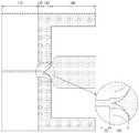
도 1은 본 발명의 바람직한 일 실시예에 따른 마이크로스트립 선로와 서스펜디드 스트립선로간 전이구조에 대한 평면도를 나타낸 것으로, 실선은 기판 윗면을 나타낸 것이고, 점선은 기판 아랫면을 나타낸 것이다.Figure 1 shows a plan view of the transition structure between the microstrip line and the suspended strip line according to an embodiment of the present invention, the solid line shows the upper surface of the substrate, the dotted line shows the lower surface of the substrate.
도 2는 도 1에 도시된 마이크로스트립 선로와 서스펜디드 스트립선로간 전이구조의 윗면(a)과 아랫면(b)을 나타낸 것이다.FIG. 2 shows the top surface (a) and the bottom surface (b) of the transition structure between the microstrip line and the suspended strip line shown in FIG. 1.
도 1 및 도 2를 참조하면, 마이크로스트립 선로과 SSL간 전이구조는 제1 CPW(120) 및 제2 CPW(130)를 포함한다.1 and 2, the transition structure between the microstrip line and the SSL includes a
제1 CPW(120)는 마이크로스트립 선로(110)에서 제2 CPW(130)로 신호를 전이하기 위한 구성으로, 기판 윗면에 형성된 제1 신호라인(121)과 제1, 제2 접지라인(122, 123) 및 기판 아랫면에 형성된 제1 접지면(125)을 포함한다.The
제1 신호라인(121)은 일단이 마이크로스트립 선로(110)의 신호라인(111)과 연결되고 다른 일단이 제2 CPW(130)의 제2 신호라인(131)과 연결되어 마이크로스트립 선로(110)의 신호라인(111)과 제2 CPW(130)의 제2 신호라인(131) 사이의 신호를 전송한다.One end of the
제1, 제2 접지라인(122, 123)은 제1 신호라인(121)과 일정 간격으로 평행하게 대칭되도록 형성되고, 적어도 하나 이상의 비아(124)를 통해 제1 접지면(125)과 연결된다.The first and
이때, 제1, 제2 접지라인(122, 123) 상에 형성된 비아(124)는 제1 신호라인(121) 방향으로 형성될 수도 있고, 제1 신호라인(121)의 수직 방향으로 형성될 수도 있는데, 자연스러운 전계 천이를 위해 비아가 생성되는 위치가 결정될 수도 있다.In this case, the
또한, 제1, 제2 접지라인(122, 123)은 SSL의 접지 역할을 수행하는 하우징과 연결되는 것이 바람직하다.In addition, the first and
제1 접지면(125)은 마이크로스트립 선로(110)의 접지면(112)과 일단이 연결되고 다른 일단이 제2 CPW(130)의 제2 접지면(135)과 연결되며, 적어도 하나 이상의 비아(124)를 통해 제1, 제2 접지라인(122, 123)과 연결된다.The
이때, 제1 접지면(125)은 마이크로스트립 선로의 접지면(112)과 동일한 형상을 가질 수 있으며, SSL을 형성하기 위한 하우징과 연결될 수 있다.In this case, the
제2 CPW(130)는 제1 CPW(120)에서 SSL(140)로 전계를 자연스럽게 전이하기 위한 구성으로, 기판 윗면에 형성된 제2 신호라인(131)과 제3, 제4 접지라인(132, 133) 및 기판 아랫면에 형성된 제2 접지면(135)을 포함한다.The
제2 신호라인(131)은 일단이 제1 신호라인(121)과 연결되고 다른 일단이 SSL(140)의 신호라인(141)과 연결되어 제1 신호라인(121)과 SSL의 신호라인(141) 사이의 신호를 전송한다.One end of the
이때, 제2 신호라인(131)은 제1 신호라인(121)과 연결된 일단의 폭이 SSL의 신호라인(141)과 연결된 다른 일단의 폭보다 작게 형성되는 것이 바람직하고, 일단 에서 다른 일단으로 갈수록 그 폭이 점점 증가하는 형상을 갖는 것이 바람직하다.In this case, it is preferable that the width of one end of the
또한, 제2 신호라인(131)은 제1 CPW(120)와 SSL(140)간의 자연스러운 전계 분포의 전이를 달성하기 위해, 다른 일단의 폭이 일단의 폭보다 큰 테이퍼형으로 형성될 수 있으며, 보다 바람직하게 특성 임피던스의 정합 형상이 클로펜스타인(Klopfenstein) 테이퍼형이 되도록 곡면이 형성될 수도 있다.In addition, the
물론, 제2 신호라인(131)은 제1 CPW의 제1 신호라인(121)과 SSL의 신호라인(141)간의 폭 차이를 고려하여 SSL 방향으로 갈수록 그 폭이 점점 증가하는 형상을 통해 특성 임피던스 및 전계의 자연스러운 전이를 달성하게 된다.Of course, the
제3, 제4 접지라인(132, 133)은 제2 신호라인(131)과 일정 간격으로 대칭되도록 형성되어 제1, 제2 접지 라인(122, 123)과 각각 연결되며 적어도 하나 이상의 비아(134)를 통해 제2 접지면(135)과 연결된다.The third and
이때, 제3, 제4 접지라인(132, 133)은 제2 신호라인(131)의 형상에 따라 제1 CPW(120)에 인접한 부분의 접지라인 간의 간격이 SSL(140)에 인접한 부분의 접지라인 간의 간격보다 작게 형성될 수 있다.In this case, the third and
또한, 제3, 제4 접지라인(132, 133) 상에 형성된 비아(134)는 제2 신호라인(131) 방향으로 형성될 수도 있고, 제2 신호라인(131)의 수직 방향으로 형성될 수도 있는데, 자연스러운 전계 전이를 위해 비아가 생성되는 위치가 결정될 수도 있다. 물론, 제3, 제4 접지라인(132, 133)은 제1, 제2 접지라인(122, 123)과 마찬가지로 SSL의 접지 역할을 수행하는 하우징과 연결되는 것이 바람직하다.In addition, the
제2 접지면(135)은 제1 접지면(125)과 연결되고 제1 CPW(120)에서 SSL(140) 방향으로 갈수록 제2 신호라인(131) 위치를 중심으로 분리되는 형상을 가지며, 제3, 제4 접지 라인(132, 133)과 적어도 하나 이상의 비아(134)를 통해 연결된다.The
이때, 제2 접지면(135)의 분리되는 형상은 SSL(140) 방향으로 갈수록 제2 접지라인(131)과 겹치지 않는 형상을 갖는 것이 바람직한다. 즉, 제2 CPW(130)는 제2 접지면(135)의 분리되는 형상으로 인해 제1 CPW(120)에서 SSL(140) 방향으로 갈수록, 제2 신호라인(131)의 아랫면에 접지가 형성되는 CBCPW(conductor-backed CPW)에서 제2 신호라인(131)의 아랫면에 접지가 형성되지 않은 CPW로 변화되는 형상을 갖는다.At this time, the shape of the
이런 제2 접지면(135)은 제1 접지면(125)과 마찬가지로 SSL을 형성하기 위한 하우징과 연결되는 것이 바람직하며, 최적의 임피던스 정합을 이루기위해 클로펜스타인(Klopfenstein) 테이퍼형이 되도록 접지면의 곡면이 형성될 수 있다.This
본 발명의 전이구조에서 제2 신호라인과 제2 접지면의 형상에 대한 임피던스 테이퍼링이 클로펜스타인 테이퍼링(Klopfenstein tapering)이 되도록 구현할 수 있는데, 이에 한정하지 않으며, 원하는 주파수 특성을 얻기 위하여, 헤켄 테이퍼링(Hecken tapering) 등과 같은 여러 가지 임피던스 테이퍼링으로 형태를 결정할 수도 있다.Impedance tapering of the shape of the second signal line and the second ground plane in the transition structure of the present invention can be implemented to be Klopfenstein tapering, but is not limited thereto, and in order to obtain a desired frequency characteristic, Hecken tapering The shape can also be determined by various impedance tapering, such as Hecken tapering.
비록, 도 1 및 도 2에서 선로 각각의 폭과 길이가 상이하게 설정되어 있지만, 이 폭과 길이는 최적의 임피던스 정합과 자연스런 전계 분포의 전이를 고려하 여 결정될 수 있다.Although the widths and lengths of the tracks are differently set in FIGS. 1 and 2, the widths and lengths may be determined in consideration of the optimum impedance matching and the transition of the natural electric field distribution.
이런 구성을 갖는 마이크로스트립 선로와 SSL간의 전이구조에 대한 자연스런 전계 분포의 전이에 대해 도 3과 도 4를 참조하여 설명한다.The transition of the natural electric field distribution for the transition structure between the microstrip line and the SSL having such a configuration will be described with reference to FIGS. 3 and 4.
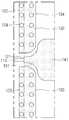
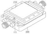
도 3은 본 발명에 대한 back-to-back 전이구조의 평면도(a), 기판 윗면에 연결되는 하우징에 대한 평면도(b), 기판 아랫면에 연결되는 하우징에 대한 평면도(c) 및 하우징이 결합된 사시도(d)를 나타낸 것이다.3 is a plan view (a) of the back-to-back transition structure according to the present invention, a plan view of the housing connected to the upper surface (b), a plan view of the housing connected to the lower surface of the substrate (c) and the housing is combined The perspective view d is shown.
도 4는 도 3에 도시된 마이크로스트립 선로와 SSL간 전이구조에서 A'A(a), B'B(b), C'C(c) 및 D'D(d)의 단면에 대한 전계 분포를 나타낸 것으로, 하우징이 결합된 상태에서의 해당 선의 단면에 대한 전계 분포를 나타낸 것이다.FIG. 4 is an electric field distribution of the cross sections of A'A (a), B'B (b), C'C (c) and D'D (d) in the transition structure between the microstrip line and SSL shown in FIG. It shows the electric field distribution for the cross section of the line in the state that the housing is coupled.
도 3의 선 A'A에서의 단면을 나타내는 도 4a에 도시된 바와 같이, 마이크로스트립 선로에서는 일부 전계가 유전체 기판의 외부에 존재하기는 하지만 대부분 신호라인(111)에서 접지면(112) 사이의 유전체 기판 내부에서 수직으로 분포하게 된다.As shown in FIG. 4A, which shows a cross section at line A'A in FIG. 3, in a microstrip line, most of the electric field is present between the
그리고, 도 3의 선 B'B의 단면을 나타내는 도 4b를 통해 알 수 있듯이, 전계 분포가 제1 CPW(120)의 제1, 제2 접지 라인(122, 123)과 비아(124)에 의해 수평 방향과 수직 방향으로 존재하고, 상부 하우징(210)의 에어갭(airgap)에 의해 상부 하우징(210)으로의 수직 및/또는 수평 방향 전계가 존재하는 것을 알 수 있다.As shown in FIG. 4B, which shows a cross section of the line B′B of FIG. 3, the electric field distribution is formed by the first and
이때, 마이크로스트립 선로(110)에서 제1 CPW(120)로 전이되는 지점에 위치한 비아(124)를 통해 접지면의 연속성을 이룰 수 있다.In this case, continuity of the ground plane may be achieved through the via 124 located at the point where the
또한, 도 3의 선 C'C의 단면을 나타내는 도 4c를 통해 알 수 있듯이, 제1 CPW(120)에서 제2 CPW(130)를 통해 SSL(140)로 전이하는 과정에서 제1 CPW(120)에서 제2 CPW(130)로의 전계를 자연스럽게 전이하기 위해, 제2 접지면(135)이 SSL(140)로 갈수록 제2 신호라인(131)을 중심으로 분리되는 갭이 커지도록 하였으며, 하부 하우징(220)은 홈이 파여져 있어 접지면에 대한 에어갭을 제공함으로써, 에어갭에 의해 하부 하우징(220)으로의 수직 및/또는 수평 방향 전계가 존재하는 것을 알 수 있다.In addition, as shown in FIG. 4C, which illustrates a cross-section of the line C′C of FIG. 3, the
마지막으로, 도 3의 선 D'D의 단면을 나타내는 도 4d를 통해 알 수 있듯이, 제2 CPW(130)의 제2 신호라인(131) 폭을 점점 크게함으로써, 일정한 특성 임피던스에 대하여 SSL 신호선로의 폭이 마이크로스트립 선로의 신호라인이나 CPW의 신호라인 폭에 비해 비교적으로 큰 SSL로 전계 분포의 자연스러운 천이를 이루도록 한다.Finally, as can be seen from FIG. 4D showing the cross-section of the line D'D in FIG. 3, the SSL signal line has a constant characteristic impedance by gradually increasing the width of the
이때, SSL의 신호라인(141) 폭이 다른 선로의 신호라인 폭에 비해 큰 이유는 신호라인으로부터 접지면까지의 높이가 비교적 높고, 전자파에 의한 신호전파가 대부분 공기매질을 통한 전파로 인해 유효 유전율이 낮기 때문이다.At this time, the width of the
이와 같이, 본 발명에 따른 전이구조는 CBCPW인 제1 CPW와, 신호라인의 폭이 SSL로 갈수록 증가하고 접지면이 신호라인을 중심으로 분리되는 형상을 갖는 제2 CPW를 이용하여 마이크로스트립 선로와 SSL간에 특성 임피던스를 최적으로 정합할 뿐 아니라 전계를 자연스럽게 전이시킴으로써, 이를 통해 Q 값(품질계수)이 향상되는 필터 및 다양한 응용 모듈을 구현할 수 있다.As described above, the transition structure according to the present invention is a microstrip line using a first CPW which is a CBCPW, and a second CPW having a shape in which the width of the signal line increases toward SSL and the ground plane is separated from the signal line. By optimally matching the characteristic impedance between SSLs, and by naturally shifting the electric field, it is possible to implement filters and various application modules which improve the Q value (quality factor).
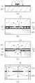
도 5는 도 3a에 구현된 마이크로스트립 선로와 SSL간 전이구조에 따른 S-파라미터를 시뮬레이션 한 결과와 측정한 결과를 나타내고 있는데, 굵은 곡선은 측정 결과로서의 입력 반사 계수 및 순방향 전달 계수(S11, S21)를 나타내고 있고, 가는 곡선은 시뮬레이션 결과로서의 입력 반사 계수 및 순방향 전달 계수(S11', S21')를 나타내고 있다.FIG. 5 shows simulation results and measured results of the S-parameter according to the transition structure between the microstrip line and SSL implemented in FIG. 3A. The thick curves show input reflection coefficients and forward transfer coefficients (S11 and S21) as measurement results. ), And the thin curve shows the input reflection coefficients and the forward transfer coefficients S11 'and S21' as simulation results.
도 5의 측정 결과를 나타내는 전이구조를 구현하는데 사용된 기판은 두께가 8[mil](혹은 0.2 mm)인 Rogers 사의 RT/Duroid 4003 기판이고, 상대 유전율은 3.38, 유전체의 손실계수는 0.0027이다.The substrate used to implement the transition structure showing the measurement result of FIG. 5 is a Rogers RT / Duroid 4003 substrate having a thickness of 8 [mil] (or 0.2 mm). The relative permittivity is 3.38 and the dielectric loss factor is 0.0027.
이런 시뮬레이션 결과와 측정 결과를 통해, 본 발명에 따른 마이크로스트립 선로와 SSL간의 전이구조는 DC 근처부터 19.5[GHz]까지의 대역에서 1.2[dB] 이하의 삽입 손실을 가지며, 10[dB] 이상의 반사손실을 가지고 있음을 알 수 있다.Through these simulation results and measurement results, the transition structure between the microstrip line and the SSL according to the present invention has an insertion loss of 1.2 [dB] or less in the band from near DC to 19.5 [GHz], and reflects 10 [dB] or more. It can be seen that there is a loss.
여기서, 시뮬레이션 결과와 측정 결과의 차이 및 16[GHz] 이상의 대역에서의 성능 열화는 회로 제작 오차와 사용된 기판의 손실계수(loss tangent=0.0027)에 의한 것이라고 볼 수 있다.Here, the difference between the simulation result and the measurement result, and the performance deterioration in the band of 16 [GHz] or more may be attributed to the circuit fabrication error and the loss factor (loss tangent = 0.0027) of the substrate used.
또한, 전이구조에 연결되는 커넥터에 의한 손실을 알아보기 위해, 본 발명의 전이구조와 동일한 길이의 50[Ω] 마이크로스트립 선로를 커넥터를 포함하여 측정한 결과, 삽입손실은 1.2[dB] 정도의 값을 가지며, 따라서 본 발명에서 제안된 전이구조에 의한 삽입손실은 매우 적은 것을 확인할 수 있다.In addition, in order to determine the loss caused by the connector connected to the transition structure, a 50 [Ω] microstrip line having the same length as the transition structure of the present invention was measured including the connector, and the insertion loss was about 1.2 [dB]. It is confirmed that the insertion loss due to the transition structure proposed in the present invention is very small.
이런 본 발명에 따른 마이크로스트립 선로와 SSL간 전이구조를 적용하여 구현할 수 있는 여러 가지 응용 모듈이 있을 수 있는데, 그 예로서 SSL 필터, SSL 다이플렉서 등을 들 수 있다.There may be various application modules that can be implemented by applying the transition structure between the microstrip line and the SSL according to the present invention, for example, an SSL filter, an SSL diplexer, and the like.
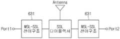
도 6은 본 발명에 따른 마이크로스트립 선로와 SSL간 전이구조가 적용된 응용 모듈에 대한 일 예들을 나타낸 것으로, 도 6a는 본 발명에 따른 마이크로스트립 선로와 SSL간(MSL-SSL) 전이구조가 사용될 수 있는 SSL 필터 모듈에 대한 일 실시예를 나타낸 것이고, 도 6b는 본 발명에 따른 MSL-SSL 전이구조가 사용될 수 있는 SSL 대역 통과 필터 모듈에 대한 일 실시예를 나타낸 것이며, 도 6c는 본 발명에 따른 MSL-SSL 전이구조가 사용될 수 있는 다이플렉서 모듈에 대한 일 실시예를 나타낸 것이다.6 illustrates an example of an application module to which a transition structure between the microstrip line and the SSL according to the present invention is applied, and FIG. 6A illustrates a transition between the microstrip line and the SSL (MSL-SSL) according to the present invention. Figure 6b shows an embodiment of the SSL filter module, Figure 6b shows an embodiment of the SSL band pass filter module that can be used MSL-SSL transition structure according to the present invention, Figure 6c according to the present invention One embodiment for a diplexer module in which the MSL-SSL transition structure can be used is shown.
SSL 필터는 도 6a에 도시된 바와 같이, SSL 필터 예를 들어 SSL 대역 통과 필터의 양단에 본 발명에 따른 MSL-SSL 전이구조(611)를 사용하면 다양한 마이크로스트립 기반의 회로와 쉽게 연결이 가능한 필터를 구현할 수 있다.As shown in FIG. 6A, the SSL filter can be easily connected to various microstrip-based circuits by using the MSL-
SSL 대역 통과 필터는 도 6b에 도시된 바와 같이, SSL 저역 통과 필터(622)와 SSL 고역 통과 필터(623)를 연속하여 연결하고, 연결된 두 필터의 양단에 본 발명에 따른 MSL-SSL 전이구조(621)를 적용함으로써, SSL 대역 통과 필터를 구현할 수 있다.As shown in FIG. 6B, the SSL band pass filter continuously connects the SSL
물론, SSL 대역 통과 필터 또한 MSL-SSL 전이구조를 사용하여 구현하기 때문에 마이크로스트립 기반의 회로와 쉽게 연결이 가능하다.Of course, the SSL bandpass filter is also implemented using the MSL-SSL transition structure, making it easy to connect with microstrip-based circuits.
SSL 다이플렉서(diplexer)는 도 6c에 도시된 바와 같이, SSL 다이플렉서의 양단에 본 발명에 따른 MSL-SSL 전이구조(631)를 사용하여 다양한 마이크로스트립 기반의 회로와 쉽게 연결이 가능하고, 이를 통해 저손실 고선택도의 다이플렉서를 구현할 수 있다.The SSL diplexer can be easily connected to various microstrip based circuits by using the MSL-
물론, 본 발명에 따른 MSL-SSL 전이구조가 도 6에서 예를 들어 설명한, SSL 필터 모듈 및 SSL 다이플렉서 모듈로 한정되는 것은 아니며, 본 발명의 MSL-SSL 전이구조가 사용될 수 있는 모든 응용 모듈에서 사용될 수 있다는 것은 이 기술분야에 종사하는 당업자에게 있어서 자명하다.Of course, the MSL-SSL transition structure according to the present invention is not limited to the SSL filter module and the SSL diplexer module described by way of example in FIG. 6, and all application modules in which the MSL-SSL transition structure of the present invention can be used. It can be used in the art will be apparent to those skilled in the art.
본 발명에 의한, 마이크로스트립 선로와 서스펜디드 스트립선로간 전이구조 및 그 응용 모듈은 본 발명의 기술적 사상의 범위 내에서 다양한 형태로 변형, 응용 가능하며 상기 실시 예에 한정되지 않는다. 또한, 상기 실시 예와 도면은 발명의 내용을 상세히 설명하기 위한 목적일 뿐, 발명의 기술적 사상의 범위를 한정하고자 하는 목적은 아니며, 이상에서 설명한 본 발명은 본 발명이 속하는 기술분야에서 통상의 지식을 가진 자에 있어 본 발명의 기술적 사상을 벗어나지 않는 범위 내에서 여러 가지 치환, 변형 및 변경이 가능하므로 상기 실시 예 및 첨부된 도면에 한정되는 것은 아님은 물론이며, 후술하는 청구범위뿐만이 아니라 청구범위와 균등 범위를 포함하여 판단되어야 한다.According to the present invention, the transition structure between the microstrip line and the suspended strip line and its application module can be modified and applied in various forms within the scope of the technical idea of the present invention and are not limited to the above embodiments. In addition, the embodiments and drawings are merely for the purpose of describing the contents of the invention in detail, not intended to limit the scope of the technical idea of the invention, the present invention described above is common knowledge in the technical field to which the present invention belongs As those skilled in the art can have various substitutions, modifications, and changes without departing from the spirit of the present invention, it is not limited to the embodiments and the accompanying drawings. And should be judged to include equality.
도 1은 본 발명의 바람직한 일 실시예에 따른 마이크로스트립 선로와 서스펜디드 스트립선로간 전이구조에 대한 평면도를 나타낸 것이다.Figure 1 shows a plan view of the transition structure between the microstrip line and the suspended strip line according to an embodiment of the present invention.
도 2는 도 1에 도시된 마이크로스트립 선로와 서스펜디드 스트립선로간 전이구조의 윗면(a)과 아랫면(b)을 나타낸 것이다.FIG. 2 shows the top surface (a) and the bottom surface (b) of the transition structure between the microstrip line and the suspended strip line shown in FIG. 1.
도 3은 본 발명에 대한 back-to-back 전이구조의 평면도(a), 기판 윗면에 연결되는 하우징에 대한 평면도(b), 기판 아랫면에 연결되는 하우징에 대한 평면도(c) 및 하우징이 결합된 사시도(d)를 나타낸 것이다.3 is a plan view (a) of the back-to-back transition structure according to the present invention, a plan view of the housing connected to the upper surface (b), a plan view of the housing connected to the lower surface of the substrate (c) and the housing is combined The perspective view d is shown.
도 4는 도 3에 도시된 마이크로스트립 선로와 SSL간 전이구조에서 A'A(a), B'B(b), C'C(c) 및 D'D(d)의 단면에 대한 전계 분포를 나타낸 것이다.FIG. 4 is an electric field distribution of the cross sections of A'A (a), B'B (b), C'C (c) and D'D (d) in the transition structure between the microstrip line and SSL shown in FIG. It is shown.
도 5는 도 3a에 구현된 마이크로스트립 선로와 서스펜디드 스트립선로간 전이구조에 따른 S-파라미터를 시뮬레이션 한 결과와 측정한 결과를 나타낸 것이다.FIG. 5 shows simulation results and measured results of S-parameters according to the transition structure between the microstrip line and the suspended strip line implemented in FIG. 3A.
도 6은 본 발명에 따른 마이크로스트립 선로와 서스펜디드 스트립선로간 전이구조가 적용된 응용 모듈에 대한 일 예들을 나타낸 것으로, 도 6a는 본 발명에 따른 마이크로스트립 선로와 서스펜디드 스트립선로간의 전이구조가 사용될 수 있는 SSL 필터 모듈에 대한 일 실시예를 나타낸 것이고, 도 6b는 본 발명에 따른 마이크로스트립 선로와 서스펜디드 스트립선로간 전이구조가 사용될 수 있는 SSL 대역 통과 필터 모듈에 대한 일 실시예를 나타낸 것이며, 도 6c는 본 발명에 따른 마이크로스트립 선로와 서스펜디드 스트립선로간 전이구조가 사용될 수 있는 다이플렉서 모듈에 대한 일 실시예를 나타낸 것이다.6 illustrates an example of an application module to which a transition structure between a microstrip line and a suspended strip line according to the present invention is applied, and FIG. 6A illustrates a transition structure between a microstrip line and a suspended strip line according to the present invention. Figure 6b shows an embodiment of the SSL filter module, Figure 6b shows an embodiment of the SSL band pass filter module that can be used a transition structure between the microstrip line and the suspended strip line according to the present invention, Figure 6c An embodiment of a diplexer module in which the transition structure between the microstrip line and the suspended strip line according to the present invention can be used is shown.
< 도면의 주요 부분에 대한 부호의 설명 ><Description of Symbols for Main Parts of Drawings>
110: 마이크로스트립 선로110: microstrip track
120: 제1 CPW120: first CPW
130: 제2 CPW130: second CPW
140: 서스펜디드 스트립선로140: Suspended strip track
Claims (7)
Translated fromKoreanPriority Applications (1)
| Application Number | Priority Date | Filing Date | Title |
|---|---|---|---|
| KR1020090132350AKR101120043B1 (en) | 2009-12-29 | 2009-12-29 | Microstrip line-suspended stripline transition structure and application module thereof |
Applications Claiming Priority (1)
| Application Number | Priority Date | Filing Date | Title |
|---|---|---|---|
| KR1020090132350AKR101120043B1 (en) | 2009-12-29 | 2009-12-29 | Microstrip line-suspended stripline transition structure and application module thereof |
Publications (2)
| Publication Number | Publication Date |
|---|---|
| KR20110075795A KR20110075795A (en) | 2011-07-06 |
| KR101120043B1true KR101120043B1 (en) | 2012-03-22 |
Family
ID=44915748
Family Applications (1)
| Application Number | Title | Priority Date | Filing Date |
|---|---|---|---|
| KR1020090132350AExpired - Fee RelatedKR101120043B1 (en) | 2009-12-29 | 2009-12-29 | Microstrip line-suspended stripline transition structure and application module thereof |
Country Status (1)
| Country | Link |
|---|---|
| KR (1) | KR101120043B1 (en) |
Families Citing this family (12)
| Publication number | Priority date | Publication date | Assignee | Title |
|---|---|---|---|---|
| KR102591621B1 (en)* | 2016-11-21 | 2023-10-20 | 한국전자통신연구원 | Microwave power combiner |
| CN106654492B (en)* | 2016-12-23 | 2019-01-22 | 武汉邮电科学研究院 | Transition transmission line and method of the coplanar waveguide transmission line to microstrip transmission line |
| CN108987862A (en)* | 2018-07-20 | 2018-12-11 | 西安电子科技大学 | The miniaturization suspended stripline filter of high quality factor |
| KR102279192B1 (en)* | 2019-09-16 | 2021-07-16 | 충남대학교산학협력단 | Transition structure between microstrip and hollow substrate integrated waveguide |
| CN111769348B (en)* | 2020-06-12 | 2021-09-24 | 中国船舶重工集团公司第七二四研究所 | Transition structure of asymmetric strip line and microstrip line |
| KR102330936B1 (en)* | 2020-09-16 | 2021-12-02 | 엘아이지넥스원 주식회사 | Connection structure between SRR type boards and device using the same |
| CN113163579B (en)* | 2021-04-16 | 2022-09-13 | 电子科技大学 | Transition structure based on medium integrated suspension line and integrated module |
| CN113594658B (en)* | 2021-08-11 | 2022-04-08 | 上海交通大学 | Broadband Transition Structure from Grounded Coplanar Waveguide to Suspended Microstrip Line |
| CN113555656B (en)* | 2021-08-18 | 2022-03-15 | 上海交通大学 | Broadband transition structure between grounded coplanar waveguide and stripline with curved ground electrode |
| CN113745785B (en)* | 2021-09-17 | 2022-04-15 | 上海交通大学 | Back-to-back transition structure from coplanar waveguide to dielectric waveguide |
| KR102773672B1 (en)* | 2022-08-17 | 2025-02-27 | 전관일 | Band-pass filter using Micro-Electro Mechanical Systems |
| CN116315552B (en)* | 2023-03-17 | 2025-04-11 | 强一半导体(苏州)股份有限公司 | A transition structure between coplanar waveguide and microstrip line |
Citations (4)
| Publication number | Priority date | Publication date | Assignee | Title |
|---|---|---|---|---|
| JP2002043811A (en)* | 2000-07-26 | 2002-02-08 | Denso Corp | Millimeter-band high-frequency device |
| JP2004135227A (en) | 2002-10-15 | 2004-04-30 | Sumitomo Metal Electronics Devices Inc | High-frequency transmission line substrate |
| KR20060028953A (en)* | 2004-09-30 | 2006-04-04 | 한국전자통신연구원 | Trapezoidal Ultra Wideband Patch Antenna |
| JP2008147757A (en) | 2006-12-06 | 2008-06-26 | Sumitomo Metal Electronics Devices Inc | High-frequency signal transmission substrate |
- 2009
- 2009-12-29KRKR1020090132350Apatent/KR101120043B1/ennot_activeExpired - Fee Related
Patent Citations (4)
| Publication number | Priority date | Publication date | Assignee | Title |
|---|---|---|---|---|
| JP2002043811A (en)* | 2000-07-26 | 2002-02-08 | Denso Corp | Millimeter-band high-frequency device |
| JP2004135227A (en) | 2002-10-15 | 2004-04-30 | Sumitomo Metal Electronics Devices Inc | High-frequency transmission line substrate |
| KR20060028953A (en)* | 2004-09-30 | 2006-04-04 | 한국전자통신연구원 | Trapezoidal Ultra Wideband Patch Antenna |
| JP2008147757A (en) | 2006-12-06 | 2008-06-26 | Sumitomo Metal Electronics Devices Inc | High-frequency signal transmission substrate |
Also Published As
| Publication number | Publication date |
|---|---|
| KR20110075795A (en) | 2011-07-06 |
Similar Documents
| Publication | Publication Date | Title |
|---|---|---|
| KR101120043B1 (en) | Microstrip line-suspended stripline transition structure and application module thereof | |
| EP2497146B1 (en) | Low loss broadband planar transmission line to waveguide transition | |
| US6794950B2 (en) | Waveguide to microstrip transition | |
| US7336142B2 (en) | High frequency component | |
| US6441471B1 (en) | Wiring substrate for high frequency applications | |
| CN108172958B (en) | Periodic slow wave transmission line unit based on coplanar waveguide | |
| CN103633400B (en) | Microstrip duplexer based on electromagnetic hybrid coupling | |
| CN109346808B (en) | Transmission line structure based on multi-layer self-packaged suspended coplanar waveguide and microstrip hybrid | |
| KR100892024B1 (en) | Bandpass filter | |
| US4542358A (en) | Device protecting a coaxial cable against high-powered, low-frequency spurious pulses | |
| JP4671458B2 (en) | Signal line to wave guide transformer | |
| US7002433B2 (en) | Microwave coupler | |
| WO2024007717A1 (en) | Strong coupling striplines and microwave element comprising same | |
| CN118983633B (en) | A rectangular waveguide-microstrip line transition conversion circuit with a narrow-side planar probe structure | |
| CN114284677A (en) | A High Selectivity Broadband Inverting Filtering Power Divider Based on Three-wire Coupling | |
| JP2005051330A (en) | Connection structure between dielectric waveguide line and high-frequency transmission line, high-frequency circuit board using the same, and package for mounting high-frequency element | |
| JP4611811B2 (en) | Fin line type microwave band pass filter | |
| CN218677535U (en) | A Strongly Coupled Stripline Structure for Passive Components | |
| CN108288742B (en) | Radio frequency isolation gate, signal isolation method, radio frequency isolation transmission circuit and transmission method | |
| KR101157825B1 (en) | Ultra-wideband transition structure for surface mountable components and application module thereof | |
| JP4105017B2 (en) | Waveguide type dielectric filter | |
| CN115799792B (en) | A microstrip dual-frequency lightning protection circuit for Sub6G | |
| KR20050080453A (en) | Non-radiative microstrip line | |
| JP4629617B2 (en) | High frequency coupled line and high frequency filter | |
| CN220400877U (en) | Feed structure |
Legal Events
| Date | Code | Title | Description |
|---|---|---|---|
| A201 | Request for examination | ||
| PA0109 | Patent application | St.27 status event code:A-0-1-A10-A12-nap-PA0109 | |
| PA0201 | Request for examination | St.27 status event code:A-1-2-D10-D11-exm-PA0201 | |
| D13-X000 | Search requested | St.27 status event code:A-1-2-D10-D13-srh-X000 | |
| D14-X000 | Search report completed | St.27 status event code:A-1-2-D10-D14-srh-X000 | |
| E902 | Notification of reason for refusal | ||
| PE0902 | Notice of grounds for rejection | St.27 status event code:A-1-2-D10-D21-exm-PE0902 | |
| PG1501 | Laying open of application | St.27 status event code:A-1-1-Q10-Q12-nap-PG1501 | |
| E13-X000 | Pre-grant limitation requested | St.27 status event code:A-2-3-E10-E13-lim-X000 | |
| P11-X000 | Amendment of application requested | St.27 status event code:A-2-2-P10-P11-nap-X000 | |
| P13-X000 | Application amended | St.27 status event code:A-2-2-P10-P13-nap-X000 | |
| E701 | Decision to grant or registration of patent right | ||
| PE0701 | Decision of registration | St.27 status event code:A-1-2-D10-D22-exm-PE0701 | |
| GRNT | Written decision to grant | ||
| PR0701 | Registration of establishment | St.27 status event code:A-2-4-F10-F11-exm-PR0701 | |
| PR1002 | Payment of registration fee | St.27 status event code:A-2-2-U10-U11-oth-PR1002 Fee payment year number:1 | |
| PG1601 | Publication of registration | St.27 status event code:A-4-4-Q10-Q13-nap-PG1601 | |
| PN2301 | Change of applicant | St.27 status event code:A-5-5-R10-R13-asn-PN2301 St.27 status event code:A-5-5-R10-R11-asn-PN2301 | |
| R18-X000 | Changes to party contact information recorded | St.27 status event code:A-5-5-R10-R18-oth-X000 | |
| FPAY | Annual fee payment | Payment date:20141125 Year of fee payment:4 | |
| PR1001 | Payment of annual fee | St.27 status event code:A-4-4-U10-U11-oth-PR1001 Fee payment year number:4 | |
| FPAY | Annual fee payment | Payment date:20151224 Year of fee payment:5 | |
| PR1001 | Payment of annual fee | St.27 status event code:A-4-4-U10-U11-oth-PR1001 Fee payment year number:5 | |
| PR1001 | Payment of annual fee | St.27 status event code:A-4-4-U10-U11-oth-PR1001 Fee payment year number:6 | |
| P22-X000 | Classification modified | St.27 status event code:A-4-4-P10-P22-nap-X000 | |
| FPAY | Annual fee payment | Payment date:20180212 Year of fee payment:7 | |
| PR1001 | Payment of annual fee | St.27 status event code:A-4-4-U10-U11-oth-PR1001 Fee payment year number:7 | |
| P22-X000 | Classification modified | St.27 status event code:A-4-4-P10-P22-nap-X000 | |
| FPAY | Annual fee payment | Payment date:20190108 Year of fee payment:8 | |
| PR1001 | Payment of annual fee | St.27 status event code:A-4-4-U10-U11-oth-PR1001 Fee payment year number:8 | |
| PR1001 | Payment of annual fee | St.27 status event code:A-4-4-U10-U11-oth-PR1001 Fee payment year number:9 | |
| R18-X000 | Changes to party contact information recorded | St.27 status event code:A-5-5-R10-R18-oth-X000 | |
| PR1001 | Payment of annual fee | St.27 status event code:A-4-4-U10-U11-oth-PR1001 Fee payment year number:10 | |
| PC1903 | Unpaid annual fee | St.27 status event code:A-4-4-U10-U13-oth-PC1903 Not in force date:20220218 Payment event data comment text:Termination Category : DEFAULT_OF_REGISTRATION_FEE | |
| PC1903 | Unpaid annual fee | St.27 status event code:N-4-6-H10-H13-oth-PC1903 Ip right cessation event data comment text:Termination Category : DEFAULT_OF_REGISTRATION_FEE Not in force date:20220218 |