KR101118974B1 - Process and system for laser crystallization processing of film regions on a substrate to provide substantial uniformity, and a structure of such film regions - Google Patents
Process and system for laser crystallization processing of film regions on a substrate to provide substantial uniformity, and a structure of such film regionsDownload PDFInfo
- Publication number
- KR101118974B1 KR101118974B1KR1020057002863AKR20057002863AKR101118974B1KR 101118974 B1KR101118974 B1KR 101118974B1KR 1020057002863 AKR1020057002863 AKR 1020057002863AKR 20057002863 AKR20057002863 AKR 20057002863AKR 101118974 B1KR101118974 B1KR 101118974B1
- Authority
- KR
- South Korea
- Prior art keywords
- region
- thin film
- film sample
- beam pulse
- boundary
- Prior art date
- Legal status (The legal status is an assumption and is not a legal conclusion. Google has not performed a legal analysis and makes no representation as to the accuracy of the status listed.)
- Expired - Fee Related
Links
Images


Classifications
- H—ELECTRICITY
- H01—ELECTRIC ELEMENTS
- H01L—SEMICONDUCTOR DEVICES NOT COVERED BY CLASS H10
- H01L21/00—Processes or apparatus adapted for the manufacture or treatment of semiconductor or solid state devices or of parts thereof
- H01L21/02—Manufacture or treatment of semiconductor devices or of parts thereof
- H01L21/02104—Forming layers
- H01L21/02365—Forming inorganic semiconducting materials on a substrate
- H01L21/02656—Special treatments
- H01L21/02664—Aftertreatments
- H01L21/02667—Crystallisation or recrystallisation of non-monocrystalline semiconductor materials, e.g. regrowth
- H01L21/02675—Crystallisation or recrystallisation of non-monocrystalline semiconductor materials, e.g. regrowth using laser beams
- H01L21/02683—Continuous wave laser beam
- H—ELECTRICITY
- H01—ELECTRIC ELEMENTS
- H01L—SEMICONDUCTOR DEVICES NOT COVERED BY CLASS H10
- H01L21/00—Processes or apparatus adapted for the manufacture or treatment of semiconductor or solid state devices or of parts thereof
- H01L21/02—Manufacture or treatment of semiconductor devices or of parts thereof
- H01L21/02104—Forming layers
- H01L21/02365—Forming inorganic semiconducting materials on a substrate
- H01L21/02367—Substrates
- H01L21/0237—Materials
- H01L21/02422—Non-crystalline insulating materials, e.g. glass, polymers
- H—ELECTRICITY
- H01—ELECTRIC ELEMENTS
- H01L—SEMICONDUCTOR DEVICES NOT COVERED BY CLASS H10
- H01L21/00—Processes or apparatus adapted for the manufacture or treatment of semiconductor or solid state devices or of parts thereof
- H01L21/02—Manufacture or treatment of semiconductor devices or of parts thereof
- H01L21/02104—Forming layers
- H01L21/02365—Forming inorganic semiconducting materials on a substrate
- H01L21/02436—Intermediate layers between substrates and deposited layers
- H01L21/02439—Materials
- H01L21/02488—Insulating materials
- H—ELECTRICITY
- H01—ELECTRIC ELEMENTS
- H01L—SEMICONDUCTOR DEVICES NOT COVERED BY CLASS H10
- H01L21/00—Processes or apparatus adapted for the manufacture or treatment of semiconductor or solid state devices or of parts thereof
- H01L21/02—Manufacture or treatment of semiconductor devices or of parts thereof
- H01L21/02104—Forming layers
- H01L21/02365—Forming inorganic semiconducting materials on a substrate
- H01L21/02518—Deposited layers
- H01L21/02521—Materials
- H01L21/02524—Group 14 semiconducting materials
- H01L21/02532—Silicon, silicon germanium, germanium
- H—ELECTRICITY
- H01—ELECTRIC ELEMENTS
- H01L—SEMICONDUCTOR DEVICES NOT COVERED BY CLASS H10
- H01L21/00—Processes or apparatus adapted for the manufacture or treatment of semiconductor or solid state devices or of parts thereof
- H01L21/02—Manufacture or treatment of semiconductor devices or of parts thereof
- H01L21/02104—Forming layers
- H01L21/02365—Forming inorganic semiconducting materials on a substrate
- H01L21/02656—Special treatments
- H01L21/02664—Aftertreatments
- H01L21/02667—Crystallisation or recrystallisation of non-monocrystalline semiconductor materials, e.g. regrowth
- H01L21/02675—Crystallisation or recrystallisation of non-monocrystalline semiconductor materials, e.g. regrowth using laser beams
- H01L21/02678—Beam shaping, e.g. using a mask
- H—ELECTRICITY
- H01—ELECTRIC ELEMENTS
- H01L—SEMICONDUCTOR DEVICES NOT COVERED BY CLASS H10
- H01L21/00—Processes or apparatus adapted for the manufacture or treatment of semiconductor or solid state devices or of parts thereof
- H01L21/02—Manufacture or treatment of semiconductor devices or of parts thereof
- H01L21/02104—Forming layers
- H01L21/02365—Forming inorganic semiconducting materials on a substrate
- H01L21/02656—Special treatments
- H01L21/02664—Aftertreatments
- H01L21/02667—Crystallisation or recrystallisation of non-monocrystalline semiconductor materials, e.g. regrowth
- H01L21/02675—Crystallisation or recrystallisation of non-monocrystalline semiconductor materials, e.g. regrowth using laser beams
- H01L21/02686—Pulsed laser beam
- H—ELECTRICITY
- H01—ELECTRIC ELEMENTS
- H01L—SEMICONDUCTOR DEVICES NOT COVERED BY CLASS H10
- H01L21/00—Processes or apparatus adapted for the manufacture or treatment of semiconductor or solid state devices or of parts thereof
- H01L21/02—Manufacture or treatment of semiconductor devices or of parts thereof
- H01L21/02104—Forming layers
- H01L21/02365—Forming inorganic semiconducting materials on a substrate
- H01L21/02656—Special treatments
- H01L21/02664—Aftertreatments
- H01L21/02667—Crystallisation or recrystallisation of non-monocrystalline semiconductor materials, e.g. regrowth
- H01L21/02689—Crystallisation or recrystallisation of non-monocrystalline semiconductor materials, e.g. regrowth using particle beams
- H—ELECTRICITY
- H01—ELECTRIC ELEMENTS
- H01L—SEMICONDUCTOR DEVICES NOT COVERED BY CLASS H10
- H01L21/00—Processes or apparatus adapted for the manufacture or treatment of semiconductor or solid state devices or of parts thereof
- H01L21/02—Manufacture or treatment of semiconductor devices or of parts thereof
- H01L21/02104—Forming layers
- H01L21/02365—Forming inorganic semiconducting materials on a substrate
- H01L21/02656—Special treatments
- H01L21/02664—Aftertreatments
- H01L21/02667—Crystallisation or recrystallisation of non-monocrystalline semiconductor materials, e.g. regrowth
- H01L21/02691—Scanning of a beam
- H—ELECTRICITY
- H01—ELECTRIC ELEMENTS
- H01L—SEMICONDUCTOR DEVICES NOT COVERED BY CLASS H10
- H01L21/00—Processes or apparatus adapted for the manufacture or treatment of semiconductor or solid state devices or of parts thereof
- H01L21/67—Apparatus specially adapted for handling semiconductor or electric solid state devices during manufacture or treatment thereof; Apparatus specially adapted for handling wafers during manufacture or treatment of semiconductor or electric solid state devices or components ; Apparatus not specifically provided for elsewhere
- H01L21/67005—Apparatus not specifically provided for elsewhere
- H01L21/67011—Apparatus for manufacture or treatment
- H01L21/67098—Apparatus for thermal treatment
- H01L21/67115—Apparatus for thermal treatment mainly by radiation
- H—ELECTRICITY
- H10—SEMICONDUCTOR DEVICES; ELECTRIC SOLID-STATE DEVICES NOT OTHERWISE PROVIDED FOR
- H10D—INORGANIC ELECTRIC SEMICONDUCTOR DEVICES
- H10D30/00—Field-effect transistors [FET]
- H10D30/01—Manufacture or treatment
- H10D30/021—Manufacture or treatment of FETs having insulated gates [IGFET]
- H10D30/031—Manufacture or treatment of FETs having insulated gates [IGFET] of thin-film transistors [TFT]
- H10D30/0312—Manufacture or treatment of FETs having insulated gates [IGFET] of thin-film transistors [TFT] characterised by the gate electrodes
- H10D30/0314—Manufacture or treatment of FETs having insulated gates [IGFET] of thin-film transistors [TFT] characterised by the gate electrodes of lateral top-gate TFTs comprising only a single gate
- H—ELECTRICITY
- H10—SEMICONDUCTOR DEVICES; ELECTRIC SOLID-STATE DEVICES NOT OTHERWISE PROVIDED FOR
- H10D—INORGANIC ELECTRIC SEMICONDUCTOR DEVICES
- H10D30/00—Field-effect transistors [FET]
- H10D30/01—Manufacture or treatment
- H10D30/021—Manufacture or treatment of FETs having insulated gates [IGFET]
- H10D30/031—Manufacture or treatment of FETs having insulated gates [IGFET] of thin-film transistors [TFT]
- H10D30/0321—Manufacture or treatment of FETs having insulated gates [IGFET] of thin-film transistors [TFT] comprising silicon, e.g. amorphous silicon or polysilicon
- H—ELECTRICITY
- H10—SEMICONDUCTOR DEVICES; ELECTRIC SOLID-STATE DEVICES NOT OTHERWISE PROVIDED FOR
- H10D—INORGANIC ELECTRIC SEMICONDUCTOR DEVICES
- H10D30/00—Field-effect transistors [FET]
- H10D30/60—Insulated-gate field-effect transistors [IGFET]
- H10D30/67—Thin-film transistors [TFT]
- H10D30/6729—Thin-film transistors [TFT] characterised by the electrodes
- H10D30/673—Thin-film transistors [TFT] characterised by the electrodes characterised by the shapes, relative sizes or dispositions of the gate electrodes
- H10D30/6731—Top-gate only TFTs
- H—ELECTRICITY
- H10—SEMICONDUCTOR DEVICES; ELECTRIC SOLID-STATE DEVICES NOT OTHERWISE PROVIDED FOR
- H10D—INORGANIC ELECTRIC SEMICONDUCTOR DEVICES
- H10D30/00—Field-effect transistors [FET]
- H10D30/60—Insulated-gate field-effect transistors [IGFET]
- H10D30/67—Thin-film transistors [TFT]
- H10D30/674—Thin-film transistors [TFT] characterised by the active materials
- H10D30/6741—Group IV materials, e.g. germanium or silicon carbide
- H10D30/6743—Silicon
- H10D30/6745—Polycrystalline or microcrystalline silicon
- H—ELECTRICITY
- H10—SEMICONDUCTOR DEVICES; ELECTRIC SOLID-STATE DEVICES NOT OTHERWISE PROVIDED FOR
- H10D—INORGANIC ELECTRIC SEMICONDUCTOR DEVICES
- H10D86/00—Integrated devices formed in or on insulating or conducting substrates, e.g. formed in silicon-on-insulator [SOI] substrates or on stainless steel or glass substrates
- H10D86/01—Manufacture or treatment
- H10D86/021—Manufacture or treatment of multiple TFTs
- H10D86/0221—Manufacture or treatment of multiple TFTs comprising manufacture, treatment or patterning of TFT semiconductor bodies
- H10D86/0223—Manufacture or treatment of multiple TFTs comprising manufacture, treatment or patterning of TFT semiconductor bodies comprising crystallisation of amorphous, microcrystalline or polycrystalline semiconductor materials
- H10D86/0229—Manufacture or treatment of multiple TFTs comprising manufacture, treatment or patterning of TFT semiconductor bodies comprising crystallisation of amorphous, microcrystalline or polycrystalline semiconductor materials characterised by control of the annealing or irradiation parameters
- H—ELECTRICITY
- H10—SEMICONDUCTOR DEVICES; ELECTRIC SOLID-STATE DEVICES NOT OTHERWISE PROVIDED FOR
- H10D—INORGANIC ELECTRIC SEMICONDUCTOR DEVICES
- H10D86/00—Integrated devices formed in or on insulating or conducting substrates, e.g. formed in silicon-on-insulator [SOI] substrates or on stainless steel or glass substrates
- H10D86/01—Manufacture or treatment
- H10D86/021—Manufacture or treatment of multiple TFTs
- H10D86/0251—Manufacture or treatment of multiple TFTs characterised by increasing the uniformity of device parameters
- Y—GENERAL TAGGING OF NEW TECHNOLOGICAL DEVELOPMENTS; GENERAL TAGGING OF CROSS-SECTIONAL TECHNOLOGIES SPANNING OVER SEVERAL SECTIONS OF THE IPC; TECHNICAL SUBJECTS COVERED BY FORMER USPC CROSS-REFERENCE ART COLLECTIONS [XRACs] AND DIGESTS
- Y10—TECHNICAL SUBJECTS COVERED BY FORMER USPC
- Y10T—TECHNICAL SUBJECTS COVERED BY FORMER US CLASSIFICATION
- Y10T117/00—Single-crystal, oriented-crystal, and epitaxy growth processes; non-coating apparatus therefor
- Y10T117/10—Apparatus
- Y10T117/1024—Apparatus for crystallization from liquid or supercritical state
- Y10T117/1076—Apparatus for crystallization from liquid or supercritical state having means for producing a moving solid-liquid-solid zone
Landscapes
- Engineering & Computer Science (AREA)
- Physics & Mathematics (AREA)
- Condensed Matter Physics & Semiconductors (AREA)
- General Physics & Mathematics (AREA)
- Manufacturing & Machinery (AREA)
- Computer Hardware Design (AREA)
- Microelectronics & Electronic Packaging (AREA)
- Power Engineering (AREA)
- Chemical & Material Sciences (AREA)
- Optics & Photonics (AREA)
- Crystallography & Structural Chemistry (AREA)
- Materials Engineering (AREA)
- Health & Medical Sciences (AREA)
- Toxicology (AREA)
- Recrystallisation Techniques (AREA)
- Thin Film Transistor (AREA)
Abstract
Translated fromKoreanDescription
Translated fromKorean관련 출원Related application
본원은 2002년 8월 19일자로 출원된 미국 가출원 제60/405,085호에 근거한 우선권을 주장하며, 상기 문헌은 원용에 의해 본원에 통합된다.This application claims priority based on US Provisional Application No. 60 / 405,085, filed August 19, 2002, which is incorporated herein by reference.
정부 권리에 대한 고지Notice of Government Rights
미국 정부는 Defense Advanced Research Project Agency 수여번호 N66001-98-1-8913의 조건에 따라 본 발명에 대해 소정 권한을 가질 수 있다.The U.S. Government may have certain rights in the invention under the terms of Defense Advanced Research Project Agency Grant No. N66001-98-1-8913.
발명의 분야Field of invention
본 발명은 박막의 처리 기술에 관한 것으로, 특히 박막 트랜지스터("TFT")의 적어도 활성 영역을 위치시키기 위한 실질적으로 균일한 그레인 영역을 얻는 박막 처리 기술에 관한 것이다.TECHNICAL FIELD This invention relates to thin film processing techniques, and more particularly, to thin film processing techniques for obtaining a substantially uniform grain area for positioning at least an active region of a thin film transistor ("TFT").
실리콘 필름과 같은 반도체 필름은 액정 디스플레이 장치를 위한 화소를 제공하는 데에 이용되는 것으로 알려져 있다. 그러한 필름은 이전부터 엑시머 레이 저 어닐링(excimer laser annealing; "ELA") 방법을 통해 처리되어 왔다(즉, 엑시머 레이저로 조사한 다음 결정화함). 그러나, 공지된 ELA 방법을 이용하여 처리된 반도체 필름은 통상 에지 효과와 같은 미세구조상 불균일성의 문제가 있으며, 이러한 사실은 그 자체가 그러한 필름 상에 제조된 박막 트랜지스터("TFT") 장치의 불균일한 성능을 조장하는 것을 입증한다. 상기 불균일성은 일반적으로 반도체 필름을 조사하는 엑시머 레이저의 출력 에너지에서의 고유한 펄스 대 펄스 변동으로부터 유래한다. 전술한 불균일성은 그 자체가, 예를 들면, 디스플레이의 어느 한 영역에서의 화소의 휘도 수준이 다른 영역에서의 휘도에 비해 현저히 차이가 있음을 입증하는 것일 수 있다.Semiconductor films such as silicon films are known to be used to provide pixels for liquid crystal display devices. Such films have previously been treated by excimer laser annealing (“ELA”) methods (ie irradiated with excimer laser and then crystallized). However, semiconductor films processed using known ELA methods usually suffer from microstructural nonuniformities, such as edge effects, which in themselves are uneven in thin film transistor ("TFT") devices fabricated on such films. Demonstrates promoting performance. The nonuniformity generally results from inherent pulse-to-pulse variations in the output energy of the excimer laser that irradiates the semiconductor film. The aforementioned nonuniformity may itself be to demonstrate, for example, that the luminance level of a pixel in one region of the display is significantly different compared to the luminance in another region.
반도체 박막의 결정화 영역에서의 불균일성을 감소시키거나 배제하려는 시도에서 "종래의" ELA(라인-빔 ELA라고도 알려져 있음) 공정의 개선을 위해 그동안 많은 노력이 경주되어 왔다. 예를 들면, Maegawa 등에 허여된 미국특허 제5,766,989호(개시된 모든 사항은 원용에 의해 본 명세서에 포함됨)에는 다결정 박막의 형성 방법 및 박막 트랜지스터의 제조 방법이 기재되어 있다. 이 문헌은 기판의 여러 가지 특성들의 균일성 문제점을 제기하고, 그러한 불균일성을 억제하기 위한 특정한 옵션을 제공하고자 하는 것이다.Many efforts have been made to improve the "traditional" ELA (also known as line-beam ELA) process in attempts to reduce or eliminate non-uniformity in the crystallization region of semiconductor thin films. For example, U. S. Patent No. 5,766, 989 to Maegawa et al., All of which is incorporated herein by reference, describes a method of forming a polycrystalline thin film and a method of manufacturing a thin film transistor. This document raises the issue of uniformity of various properties of the substrate and provides specific options for suppressing such nonuniformities.
그러나, 종래의 ELA 방법에서 사용된 빔-형성 접근방법의 구체적 사항은 반도체 필름의 불균일성을 감소하는 것을 매우 어렵게 한다. 이는 특히 전술한 에너지 플루언스(fluence)가 각각의 빔 펄스에 대해 다를 수 있고, 그에 따라 불균일성이 조사, 응고 및 결정화 시에 반도체 박막의 섹션에 도입될 수 있기 때문이다.However, the details of the beam-forming approach used in the conventional ELA method make it very difficult to reduce the nonuniformity of the semiconductor film. This is especially because the energy fluences described above may be different for each beam pulse, so that non-uniformities can be introduced into sections of the semiconductor thin film upon irradiation, solidification and crystallization.
순차적 횡방향 응고를 이용하여 큰 그레인형 단결정 또는 다결정 실리콘 박막을 제조하는 기술은 이미 공지되어 있다. 예를 들면, Im에 허여된 미국특허 제6,322,625호 및 미국특허 출원 제09/390,537호(이들 문헌의 모든 개시 내용은 원용에 의해 본 명세서에 포함되며, 본원의 공동 양수인에게 양도되어 있음)에는, 에너지 제어형 레이저 펄스 및 순차적 횡방향 응고를 구현하기 위한 실리콘 샘플의 소규모 평행이동(translation)을 이용한 큰 그레인 다결정 또는 단결정 실리콘 구조체를 성장시키는 특히 바람직한 장치 및 방법이 기재되어 있다. 이들 특허문헌에는, 기판 상의 반도체 필름의 적어도 일부를 그 두께 전체에 걸쳐 필름의 상기 부분을 완전히 용융시키기 위해 적합한 조사 펄스로 조사하는 것에 대하여 구체적으로 설명되어 있다. 이러한 방식으로, 용융된 반도체 물질이 응고되면, 결정 구조는 완전히 용융되지 않은 반도체 필름의 선택된 영역으로부터 응고 부분(solidifying portion)으로 성장해 간다. 이 문헌은 핵형성이 일어날 수 있는 영역에서는 작은 그레인이 성장된다고 설명한다. 공지되어 있는 바와 같이, 그러한 핵형성은 핵형성 영역에서 작은 그레인으로 이루어진 물질을 발생시킨다.Techniques for producing large grain monocrystalline or polycrystalline silicon thin films using sequential transverse solidification are already known. For example, U. S. Patent No. 6,322, 625 to U.S. Patent Application Serial No. 09 / 390,537, all disclosures of which are incorporated herein by reference, and assigned to the joint assignee herein, Particularly preferred apparatus and methods for growing large grain polycrystalline or single crystal silicon structures using energy controlled laser pulses and small scale translation of silicon samples to achieve sequential transverse coagulation are described. These patent documents specifically describe irradiating at least a portion of a semiconductor film on a substrate with a suitable irradiation pulse to completely melt the portion of the film over its entire thickness. In this way, once the molten semiconductor material solidifies, the crystal structure grows from a selected region of the semiconductor film that is not completely melted into a solidifying portion. This document explains that small grains grow in areas where nucleation can occur. As is known, such nucleation results in a material consisting of small grains in the nucleation region.
미국특허 제6,322,625호에 설명되어 있는 바에 따르면 단면적이 큰 빔 펄스를 이용하여 특정 영역의 조사 공정을 활용하는 순차적 횡방향 응고(sequential lateral solidification; "SLS")에 대한 당업자에게 이미 공지되어 있는 바와 같이, 그러한 영역에서 횡방향 결정이 성장되기 전에 핵형성이 일어날 수 있다. 이것은 일반적으로 바람직하지 않다고 생각되며, 따라서 이들 영역 내에 TFT 장치를 위치시키는 것을 피해왔다.As described in U.S. Patent No. 6,322,625, as is already known to those skilled in the art for sequential lateral solidification ("SLS") utilizing a specific area of irradiation process using beam pulses having a large cross-sectional area. In such regions, nucleation can occur before transverse crystals grow. This is generally considered undesirable, and thus avoiding positioning the TFT device in these areas.
TFT 장치에 따라서는 고수준의 성능을 필요로 하지 않지만, 그러한 TFT 장치가 특정 응용에서는 양호한 균일성을 필요로 한다. 따라서, 반도체 박막 상의 동일한 영역을 다중 조사하지 않고도 균일한 작은 그레인으로 이루어진 물질을 박막 내에 생성할 수 있는 반도체 박막을 포함하는 기판을 제조하는 것이 바람직하다.Some TFT devices do not require a high level of performance, but such TFT devices require good uniformity in certain applications. Therefore, it is desirable to manufacture a substrate comprising a semiconductor thin film that can produce a material of uniform small grains in the thin film without multiple irradiation of the same region on the semiconductor thin film.
발명의 요약Summary of the Invention
따라서, 본 발명의 목적 중 하나는, TFT 장치를 위치시킬 수 있도록 기판 필름 상에 대체로 균일한 영역을 형성할 수 있는 개선된 방법 및 시스템을 제공하는 것이다. 본 발명의 또 다른 목적은 상기 영역이 핵형성되고(빔 펄스의 임계 상태에 기초하여) 이어서 응고되도록 함으로써, 재응고되었을 때 상기 핵형성 영역은 균일하고 작은 그레인으로 이루어진 물질을 가진 영역이 되도록 하는 것이다. 본 발명의 또 다른 목적은 반도체 필름을 액정 디스플레이 또는 유기 발광 다이오드 디스플레이에 이용하기 위해 처리하는 속도를 높이는 것이다. 본 발명의 또 다른 목적은 반도체 박막의 조사된 영역 각각이, 그 실질적 부분을 재조사(re-irradiation)할 필요 없이 1회의 조사로 양호한 물질을 제공할 수 있도록 하는 것이다.Accordingly, one of the objects of the present invention is to provide an improved method and system capable of forming a generally uniform area on a substrate film to position a TFT device. Another object of the present invention is to allow the region to nucleate (based on the critical state of the beam pulse) and then to solidify so that when resolidified, the nucleation region becomes a region with a material of uniform, small grains. will be. Another object of the present invention is to speed up the processing of semiconductor films for use in liquid crystal displays or organic light emitting diode displays. It is still another object of the present invention that each of the irradiated regions of the semiconductor thin film can provide a good material in a single irradiation without having to re-irradiate a substantial portion thereof.
이하에 제시되는 설명을 참조하여 명백해지는 바와 같이 상기 목적 및 그 밖의 태양 중 적어도 일부에 따르면, 핵형성되고 작은 그레인으로 이루어진 물질이 매우 양호한 균일성(예; 균일한 그레인)을 갖는 것으로 밝혀졌다. 또한, 그러한 핵형성 영역에서의 그레인 사이즈는 이러한 영역을 용융시키는 빔 펄스의 에너지 밀도의 변동이 심한 경우에도 크게 변동되지 않는 것이 확인되었다. 이것은 특히 이들 영역을 그 두께 전체에 걸쳐 완전히 용융하는 데 필요한 임계치 이상으로 빔의 에너지 밀도가 유지될 때 그러하다. 예를 들면, 두께가 약 0.1㎛인 반도체 박막의 경우에, 빔 펄스 각각의 에너지 밀도는 50 mJ/㎠보다 높아야 한다. 또한, 빔의 최소 세기가 전술한 임계치보다 높다면 반도체 박막에 입사되는 빔의 입체적 불균일성에 대해 박막의 균일성은 민감하지 않은 것으로 밝혀졌다.According to at least some of the above objects and other aspects, as will become apparent with reference to the description given below, it has been found that a nucleated, small grain material has very good uniformity (eg, uniform grain). It was also confirmed that the grain size in such nucleation regions does not vary greatly even when the variation in the energy density of the beam pulses melting these regions is severe. This is especially true when the energy density of the beam is maintained above the threshold needed to melt these regions completely throughout its thickness. For example, in the case of a semiconductor thin film having a thickness of about 0.1 μm, the energy density of each beam pulse should be higher than 50 mJ / cm 2. In addition, it has been found that the uniformity of the thin film is insensitive to the steric nonuniformity of the beam incident on the semiconductor thin film if the minimum intensity of the beam is higher than the aforementioned threshold.
본 발명의 예시적 구현예에서, 반도체 박막 샘플의 처리 방법 및 시스템이 제공된다. 특히, 빔 발생기는 적어도 하나의 빔 펄스를 방출하도록 제어될 수 있다. 이 빔 펄스를 이용하여, 샘플의 섹션을 그 두께 전체에 걸쳐 완전히 용융시키기에 충분한 세기로 박막 샘플의 적어도 한 부분을 조사한다. 상기 빔 펄스는 소정의 형상을 가질 수 있다. 박막 샘플의 이 부분은 재응고되며, 재응고된 부분은 제1 영역과 제2 영역으로 이루어진다. 재응고가 이루어지면, 제1 영역은 큰 그레인을 포함하고, 제2 영역은 핵형성을 통해 형성된 작은 그레인 영역을 갖는다. 제1 영역은 제2 영역을 둘러싸고 있고, 제2 영역의 그레인 구조와 상이한 그레인 구조를 갖는다. 제2 영역은 박막 트랜지스터("TFT")의 활성 영역을 수용할 수 있게 되어 있다.In an exemplary embodiment of the invention, a method and system for processing a semiconductor thin film sample is provided. In particular, the beam generator can be controlled to emit at least one beam pulse. Using this beam pulse, at least one portion of the thin film sample is irradiated with sufficient intensity to completely melt the section of the sample throughout its thickness. The beam pulse may have a predetermined shape. This portion of the thin film sample is resolidified and the resolidified portion is comprised of a first region and a second region. When resolidification occurs, the first region comprises large grains and the second region has small grain regions formed through nucleation. The first region surrounds the second region and has a grain structure different from the grain structure of the second region. The second region is adapted to receive the active region of the thin film transistor ("TFT").
본 발명의 또 다른 예시적 구현예에서, 제1 영역은 제1 경계부(border) 및 제1 영역의 상기 제1 경계부에 대향하여 평행하게 제공되는 제2 경계부를 가진다. 또한, 제2 영역은 제3 경계부 및 제2 영역의 상기 제3 경계부에 대향하여 평행하게 제공되는 제4 경계부를 가진다. 제1 경계부와 제2 경계부 사이의 간격은 제3 경계부와 제4 경계부 사이의 간격보다 작다. 제2 영역은 적어도 하나의 화소에 대응하는 것이 바람직하다. 또한, 제2 영역은 TFT의 모든 부분을 수용할 수 있는 단면적을 가질 수 있다. 제1 영역의 일부분은 TFT의 작은 섹션을 수용할 수도 있다. 제2 영역에 대한 제1 영역의 크기와 위치는 제1 영역에 의해 TFT의 성능에 전혀 영향을 주지 않거나 무시할 수 있을 정도의 영향을 주도록 제공될 수 있다.In another exemplary embodiment of the present invention, the first region has a first border and a second boundary provided in parallel to the first boundary of the first region. Also, the second region has a fourth boundary portion and a fourth boundary portion provided in parallel to the third boundary portion of the second region. The spacing between the first boundary and the second boundary is smaller than the spacing between the third boundary and the fourth boundary. Preferably, the second region corresponds to at least one pixel. In addition, the second region may have a cross-sectional area that can accommodate all portions of the TFT. A portion of the first region may receive a small section of the TFT. The size and position of the first area relative to the second area can be provided by the first area to have no influence on the performance of the TFT or a negligible effect.
본 발명의 또 다른 구현예에 따르면, 박막 샘플을 소정의 거리에 걸쳐 평행이동시킬 수 있다. 추가적인 빔 펄스를 사용하여, 박막 샘플의 다른 부분을 조사할 수 있다. 상기 도 다른 부분은 상기 소정의 거리에 실질적으로 대응하는 부분으로부터 일정한 거리를 두고 제공된다. 박막 샘플의 상기 다른 부분은 재응고되며, 재응고된 부분은 제3 영역과 제4 영역으로 이루어진다. 또한, 제3 영역은 제4 영역을 둘러쌀 수 있고, 제3 영역의 적어도 하나의 섹션은 제1 영역의 적어도 하나의 섹션에 적어도 부분적으로 중첩된다. 더 나아가, 재응고가 이루어지면, 제3 영역은 횡방향으로 성장된 그레인을 가지고, 제4 영역은 핵형성된 영역을 가진다. 제4 영역은 또한 제2 영역의 에지로부터 거리를 두고 제공되어 있는 에지로 이루어질 수 있다. 더 나아가, 제4 영역은 제2 영역의 에지와 거의 경계를 이루는 에지로 이루어지고, 제4 영역의 상기 에지는 제1 영역의 어느 섹션 내로든 연장되지 않을 수 있다. 빔 펄스는 상기 추가적인 빔 펄스의 플루언스와 실질적으로 동일한(또는 상이한) 플루언스를 가질 수 있다.According to another embodiment of the present invention, the thin film sample may be parallel moved over a predetermined distance. Additional beam pulses can be used to investigate other portions of the thin film sample. The other portion is provided at a constant distance from the portion substantially corresponding to the predetermined distance. The other portion of the thin film sample is resolidified and the resolidified portion is comprised of a third region and a fourth region. Also, the third region may surround the fourth region, wherein at least one section of the third region at least partially overlaps at least one section of the first region. Furthermore, if resolidification occurs, the third region has grains grown laterally and the fourth region has nucleated regions. The fourth region may also consist of an edge provided at a distance from the edge of the second region. Furthermore, the fourth region may consist of an edge substantially bordering the edge of the second region, and the edge of the fourth region may not extend into any section of the first region. The beam pulse may have a fluence that is substantially the same (or different) as the fluence of the additional beam pulse.
본 발명의 또 다른 구현예에서, 박막 샘플을 소정의 거리에 걸쳐 평행이동시킬 수 있다. 그러면, 빔 펄스를 이용하여 상기 박막 샘플의 다른 부분을 조사할 수 있다. 상기 다른 부분은 상기 소정의 거리에 실질적으로 대응하는 부분으로부터 일정한 거리를 두고 제공된다. 박막 샘플은 사전 패터닝된(pre-patterned) 실리콘 박막 샘플이거나, 연속적 실리콘 박막 샘플일 수 있다. 또한, 박막 샘플을 소정의 거리에 걸쳐 평행이동시킬 수 있고, 적어도 하나의 빔 펄스를 이용하여 박막 샘플의 다른 부분을 조사할 수 있다. 상기 다른 부분은 상기 소정의 거리에 실질적으로 대응하는 부분으로부터 일정한 거리를 두고 제공되는 것이 바람직하다. 또한, 박막 샘플은 조사할 상기 박막 샘플의 상기 다른 부분의 제1 상대적 사전 계산된(pre-calculated) 위치에 전달할 수 있다. 상기 전달 후에, 박막 샘플은 상기 소정의 거리와 상이한 거리에 있는 제2 상대적 사전 계산된 위치에 제공될 수 있다.In another embodiment of the invention, the thin film sample can be translated over a distance. Then, another part of the thin film sample may be irradiated using the beam pulse. The other portion is provided at a constant distance from the portion substantially corresponding to the predetermined distance. The thin film sample may be a pre-patterned silicon thin film sample or a continuous silicon thin film sample. In addition, the thin film sample can be translated over a predetermined distance and at least one beam pulse can be used to irradiate another portion of the thin film sample. Preferably, the other portion is provided at a predetermined distance from the portion substantially corresponding to the predetermined distance. The thin film sample may also be delivered to a first relative pre-calculated position of the other portion of the thin film sample to be irradiated. After the transfer, a thin film sample may be provided at a second relative precomputed location that is at a different distance from the predetermined distance.
본 발명의 또 다른 구현예에 따르면, 박막 샘플은 소정의 거리에 걸쳐 재차 평행이동될 수 있다. 다음에, 박막 샘플의 평행이동은 중지될 것이고, 박막 샘플의 진동은 멈추어지게 된다. 그 후, 적어도 하나의 빔 펄스를 이용하여 박막 샘플의 다른 부분을 조사하는데, 상기 다른 부분은 상기 소정의 거리에 실질적으로 대응하는 부분으로부터 일정한 거리를 두고 제공된다. 이어서, 박막 샘플의 상기 부분을 추가적인 빔 펄스로 조사하고, 재응고시킨다. 상기 빔 펄스의 플루언스는 상기 추가적인 빔 펄스의 플루언스와 상이하다(예를 들면, 상기 빔 펄스의 플루언스 미만이다).According to another embodiment of the invention, the thin film sample may be translated again over a predetermined distance. Next, the translation of the thin film sample will be stopped, and the vibration of the thin film sample will be stopped. Thereafter, at least one beam pulse is used to irradiate another portion of the thin film sample, the other portion being provided at a constant distance from the portion substantially corresponding to the predetermined distance. The portion of the thin film sample is then irradiated with additional beam pulses and resolidified. The fluence of the beam pulse is different from the fluence of the additional beam pulse (eg, less than the fluence of the beam pulse).
본 발명의 또 다른 구현예에 따르면, 상기 제1 영역의 위치는 TFT의 활성 영역이 그 위에 위치하지 않도록 결정된다. 빔 펄스는 복수의 빔렛(beamlet)을 포함하고, 제1 및 제2 영역은 상기 빔렛에 의해 조사되는 것이 바람직하다. 반도체 박막 샘플은 실리콘 박막 샘플일 수도 있고, 실리콘, 게르마늄 또는 이들의 합금으로 이루어질 수도 있다. 반도체 박막은 약 100Å 내지 10,000Å의 두께를 가질 수 있다. 빔 펄스의 일부는 적어도 하나의 마스킹된 빔 펄스를 형성하도록 마스킹될 수 있고, 상기 마스킹된 빔 펄스는 박막 샘플의 일부분을 조사하는 데 이용될 수 있다. 제1 영역에 제공되는 큰 그레인은 횡방향 성장 그레인일 수 있고, 제1 영역의 상기 횡방향 성장 그레인은 등축(equiaxed) 그레인일 수 있다.According to another embodiment of the present invention, the position of the first region is determined so that the active region of the TFT is not located thereon. The beam pulse preferably comprises a plurality of beamlets, the first and second regions being irradiated by the beamlets. The semiconductor thin film sample may be a silicon thin film sample or may be made of silicon, germanium, or an alloy thereof. The semiconductor thin film may have a thickness of about 100 GPa to 10,000 GPa. A portion of the beam pulse may be masked to form at least one masked beam pulse, which may be used to irradiate a portion of the thin film sample. The large grains provided in the first region may be lateral growth grains and the lateral growth grains of the first region may be equiaxed grains.
본 발명의 또 다른 구현예에 따르면, 제1 영역 및 제2 영역을 가진 반도체 박막 샘플이 제공된다. 제1 영역은 큰 그레인을 갖는 것이 바람직하다. 제2 영역은 제1 영역에 의해 둘러싸여 있고, 제2 영역이 위치하고 있는 반도체 박막의 적어도 한 섹션의 핵형성을 통해 형성된 영역을 포함한다. 제1 영역의 그레인 구조는 제2 영역의 그레인 구조와 상이하다. 제2 영역은 박막 트랜지스터("TFT")의 활성 영역을 수용하도록 되어 있는 것이 바람직하다.According to yet another embodiment of the present invention, a semiconductor thin film sample having a first region and a second region is provided. It is preferable that the first region has large grains. The second region is surrounded by the first region and includes a region formed through nucleation of at least one section of the semiconductor thin film on which the second region is located. The grain structure of the first region is different from the grain structure of the second region. The second region is preferably adapted to receive the active region of the thin film transistor ("TFT").
본 발명에 포함되고 그 일부를 구성하는 첨부 도면은 본 발명의 바람직한 구현예를 예시하며 본 발명의 원리를 설명하는 역할을 한다.The accompanying drawings, which are incorporated in and constitute a part of the invention, illustrate preferred embodiments of the invention and serve to explain the principles of the invention.
도 1A는 균일하고 작은 그레인으로 이루어진 영역을 형성하도록 핵형성되고 응고되도록 샘플의 반도체 박막의 특정 영역을 조사하는 본 발명에 따른 조사 시스템의 예시적 구현예에 대한 개략적 블록도이고;1A is a schematic block diagram of an exemplary embodiment of an irradiation system according to the present invention for irradiating a specific region of a semiconductor thin film of a sample to be nucleated and solidified to form regions of uniform and small grain;
도 1B는 반도체 박막을 포함하는 샘플의 확대된 측단면도이다.1B is an enlarged side cross-sectional view of a sample including a semiconductor thin film.
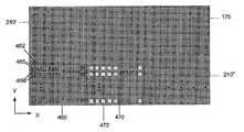
도 2는 도 1A의 예시적 시스템을 이용하여 반도체 박막의 전체 표면적에 대해 본 발명에 따른 방법이 실행되는 반도체 박막을 가지는, 개념적으로 분할된 샘플의 예시적 구현예에 대한 분해 평면도이다.FIG. 2 is an exploded top view of an exemplary embodiment of a conceptually divided sample having a semiconductor thin film in which the method according to the present invention is performed with respect to the total surface area of the semiconductor thin film using the example system of FIG. 1A.
도 3은 본 발명에 따른 마스크의 제1 예시적 구현예의 평면도로서, 상기 마스크는 하나의 개방되거나 투명한 영역을 둘러싸는 빔-블록킹 영역을 가지며, 패턴형 빔 펄스가 되도록 레이저 빔 소스에 의해 발생되는 빔 펄스를 마스킹함으로써 마스킹된 빔 펄스가 반도체 필름 상의 특정 영역을 조사하도록 하기 위해 도 1A의 예시적 시스템과 함께 이용할 수 있다.3 is a plan view of a first exemplary embodiment of a mask according to the invention, wherein the mask has a beam-blocking area surrounding one open or transparent area and is generated by a laser beam source to be a patterned beam pulse; Masking the beam pulses can be used in conjunction with the example system of FIG. 1A to cause the masked beam pulses to irradiate specific areas on the semiconductor film.
도 4A-4D는 본 발명의 방법에 따른 예시적 구현예의 여러 가지 순차적 단계에서 샘플의 제1 예시적 개념상 칼럼에 대하여,도 3의 마스크에 의해 마스킹되는 조사 빔 펄스에 의한 조사, 이어서 샘플 표면에 제공된 반도체 필름의 특정 부분의 재응고 및 결정화를 나타내는 도면이다.4A-4D illustrate irradiation with a radiation beam pulse masked by the mask of FIG. 3, followed by sample surface, for a first exemplary conceptual column of samples in various sequential steps of an exemplary embodiment according to the method of the present invention. It is a figure which shows resolidification and crystallization of the specific part of the semiconductor film provided in.
도 4E-4F는 본 발명의 방법에 따른 처리의 2개의 예시적 순차 단계에서 샘플의 제2 예시적 개념상 칼럼에 대하여, 도 3의 마스크에 의해 마스킹되는 조사 빔 펄스에 의한 조사, 이어서 샘플 표면에 제공된 반도체 필름의 특정 부분의 재응고 및 결정화를 나타내는 도면이다.4E-4F illustrate irradiation with a radiation beam pulse masked by the mask of FIG. 3, followed by a sample surface, for a second exemplary conceptual column of samples in two exemplary sequential steps of treatment in accordance with the method of the present invention. It is a figure which shows resolidification and crystallization of the specific part of the semiconductor film provided in.
도 5A는 다중 소형 개구부 또는 투명 영역 또는 슬릿을 둘러싸는 빔 블록킹 영역을 가진, 본 발명에 따른 마스크의 제2 예시적 구현예에 대한 평면도로서, 이것은 패터닝된 빔렛 내에 빔 소스에 의해 생성된 빔 펄스를 마스킹함으로써 마스킹된 빔렛 펄스가 반도체 필름 상의 특정 영역을 조사하도록 도 1A의 예시적 시스템 과 함께 이용할 수 있다.FIG. 5A is a plan view of a second exemplary embodiment of a mask according to the present invention having multiple small openings or beam blocking areas surrounding a transparent area or slit, which is a beam pulse generated by a beam source within a patterned beamlet By masking the masked beamlet pulses may be used with the example system of FIG. 1A to irradiate specific regions on the semiconductor film.
도 5B는 도 5A에 도시된 마스크의 제2 구현예의 빔렛에 대한 확대도이다.5B is an enlarged view of the beamlet of the second embodiment of the mask shown in FIG. 5A.
도 6A-6D는 본 발명의 방법에 따른 제1 예시적 구현예의 여러 가지 순차적 단계에서 샘플의 제1 예시적 개념상 칼럼에 대하여,도 5의 마스크에 의해 마스킹되는 조사 빔 펄스 강도 패턴에 의한 조사, 및 이어서 샘플 표면에 제공된 반도체 필름의 특정 부분의 재응고 및 결정화를 나타내는 도면이다.6A-6D illustrate irradiation with a radiation beam pulse intensity pattern masked by the mask of FIG. 5, for a first exemplary conceptual column of samples in various sequential steps of a first exemplary embodiment according to the method of the present invention. And, subsequently, resolidification and crystallization of specific portions of the semiconductor film provided on the sample surface.
도 7은 샘플에 제공된 반도체 박막을 예시하는 도면으로서, 상기 박막은 하나의 길고 좁은 개구부 또는 투명 영역을 둘러싸는 빔 블록킹 영역을 가진 마스크에 의해 패터닝되는 단면을 갖는 빔 펄스에 의해 조사되고, 도 1A의 예시적 시스템과 함께 이용할 수 있다.FIG. 7 is a diagram illustrating a semiconductor thin film provided in a sample, the thin film being irradiated by a beam pulse having a cross section patterned by a mask having a beam blocking area surrounding one long narrow opening or transparent area, and FIG. 1A Can be used in conjunction with an exemplary system.
도 8A는 TFT 장치 전체가 핵형성을 통해 형성된 작고 균일한 그레인으로 이루어진 영역에 위치하고 있는, 도 4D 및 6D의 영역에 대응하여 조사되고 재응고되고 결정화된 2개의 특정 영역을 예시하는 도면이다.FIG. 8A is a diagram illustrating two specific regions irradiated, resolidified and crystallized corresponding to the regions of FIGS. 4D and 6D, in which the entire TFT device is located in a region of small uniform grains formed through nucleation.
도 8B는 TFT 장치의 활성 영역의 전체 단면만이 핵형성을 통해 형성된 작고 균일한 그레인으로 이루어진 영역에 위치하는 반면 다른 영역은 결정화된 영역들 사이의 경계 영역에 걸쳐 제공되어 있는, 도 4D 및 6D의 영역에 대응하여 조사되고 재응고되고 결정화된 2개의 특정 영역을 예시하는 도면이다.Fig. 8B shows only the entire cross section of the active area of the TFT device in an area made up of small uniform grains formed through nucleation while other areas are provided across the boundary area between the crystallized areas, Figs. 4D and 6D. The figure illustrates two specific regions irradiated, resolidified and crystallized corresponding to the region of.
도 9는 도 4A-4F 및 6A-6D에 제시된 본 발명의 예시적 기법을 이용하여 도 1A의 컴퓨팅 설비를 부분적으로 제어하는 상태에서 본 발명의 예시적 처리 방법을 나타내는 흐름도이다.9 is a flow diagram illustrating an exemplary processing method of the present invention in a state of partially controlling the computing facility of FIG. 1A using the example techniques of the present invention shown in FIGS. 4A-4F and 6A-6D.
도 10은 도 4A-4F 및 6A-6D에 제시된 본 발명의 예시적 기법을 이용하여 도 1A의 컴퓨팅 설비를 부분적으로 제어하는 상태에서 본 발명의 또 다른 예시적 처리 방법을 나타내는 흐름도로서, 여기서 도 1A의 빔 소스는 빔의 충돌에 대해 반도체 필름의 위치에 기초하여 발사된다.FIG. 10 is a flow diagram illustrating another exemplary processing method of the present invention in a state of partially controlling the computing facility of FIG. 1A using the example techniques of the present invention shown in FIGS. 4A-4F and 6A-6D. The beam source of 1A is fired based on the position of the semiconductor film with respect to the collision of the beam.
본 발명에 따른 여러 가지 시스템은, 균일한 물질을 가지고 있어서 박막 트랜지스터("TFT")의 적어도 활성 영역을 해당 영역에 위치시킬 수 있는 반도체(예; 실리콘) 필름 상에 하나 이상의 영역을 생성하고, 핵형성하고, 응고시키며 결정화하는 데에 이용할 수 있음을 이해해야 한다. 그러한 영역을 얻기 위한 시스템 및 방법, 그리고 얻어지는 결정화 반도체 박막의 예시적 구현예를 이하에서 더 설명하기로 한다. 그러나, 본 발명은 여기에서 설명하는 반도체 박막의 시스템 및 방법의 예시적 구현예에 한정되지 않음을 이해해야 할 것이다.Various systems in accordance with the present invention generate one or more regions on a semiconductor (eg, silicon) film having a uniform material and capable of positioning at least an active region of a thin film transistor (“TFT”) in that region, It should be understood that it can be used to nucleate, coagulate and crystallize. Systems and methods for obtaining such regions, and exemplary embodiments of the resulting crystallized semiconductor thin film are described further below. However, it should be understood that the present invention is not limited to the exemplary embodiments of the systems and methods of semiconductor thin films described herein.
연속 동작 SLS를 제공하기 위한 특정 시스템이 미국특허 출원번호 제09/526,585호(이하, "'585 출원"이라 함)에 기재되어 있으며, 이의 개시 내용 전체는 원용에 의해 본원에 통합된다. 본 발명의 예시적 구현예에 따른 실질적으로 유사한 시스템을 이용하여, TFT 장치의 활성 영역을 위치시킬 수 있는 전술한 반도체 박막의 핵형성되고, 응고되며 결정화된 부분을 행성할 수 있다.Certain systems for providing continuous operation SLS are described in US Patent Application Serial No. 09 / 526,585 (hereinafter referred to as the "'585 Application"), the entire disclosure of which is incorporated herein by reference. Using a substantially similar system according to an exemplary embodiment of the present invention, it is possible to planet the nucleated, solidified and crystallized portion of the above-described semiconductor thin film that can position the active region of the TFT device.
구체적으로, 본 발명에 따른 시스템은, 반도체 박막의 특정 영역의 핵형성, 이어지는 응고 및 결정화를 촉진하도록 조사 빔 펄스에 의해 조사되는 비정질 실리콘 박막을 가진 샘플(170) 상에 이용한다. 상기 예시적 시스템은 조사용 빔(예; 레이저 빔)을 방출하는 빔 소스(110)(예; Lambda Physik Model LPX-3151 XeCl 펄스형 엑시머 레이저), 레이저 빔의 에너지 밀도를 변조하기 위한 제어 가능한 빔 에너지 밀도 변조기(120), MicroLas 2 플레이트 가변 감쇠기(130), 빔 조종용 거울(beam steering mirror)(140, 143, 147, 160, 162), 빔 확장 및 조준 렌즈(141, 142), 빔 호모게나이저(144), 집광 렌즈(145), 필드 렌즈(148), 평행이동 스테이지(translating stage)(도시되지 않음)에 장착될 수 있는 프로젝션 마스크(150), 4×~6× 대안 렌즈(161), 제어 가능형 셔터(152), 샘플 평행이동 스테이지(180)에 장착된 반도체 박막을 처리하는 샘플(170)에 대한 조사 빔 펄스(164)의 초점을 맞추는 멀티엘리먼트 대물 렌즈(163), 진동 격리 및 자동 레벨링 시스템(191, 192, 193, 194) 상에 지지되는 화강암 블록 광학 벤치(190), 및 빔 소스(110), 빔 에너지 밀도 변조기(120), 가변 감쇠기(130), 셔터(152) 및 샘플 평행이동 스테이지(180)를 제어하도록 결합된 컴퓨터 장치(computing arrangement)(100)(예; 본 발명에 따른 프로그램을 실행하는 범용 컴퓨터 또는 특수 목적 컴퓨터)를 포함한다.In particular, the system according to the present invention is used on a
샘플 평행이동 스테이지(180)는 샘플(170)의 평면 X-Y 방향뿐 아니라 Z 방향으로 평행이동시키도록 컴퓨터 장치(100)에 의해 제어되는 것이 바람직하다. 이 방식으로, 컴퓨터 장치(100)는 조사 빔 펄스(164)에 대한 샘플(40)의 상대적 위치를 제어한다. 반복 동작 및 조사 빔 펄스(164)의 에너지 밀도도 컴퓨터(100)에 의해 제어된다. 당업자는 빔 소스(110)(예; 펄스형 엑시머 레이저) 대신에 상기 조사 빔 펄스는 이하에서 설명하는 방식으로 샘플(170)의 반도체(예; 실리콘) 박막의 선택된 영역의 전체 두께를 완전히 용융시키는 데 적합한 짧은 에너지 펄스의 또 다른 공지된 소스에 의해 생성될 수 있음을 이해해야 한다. 상기 공지된 소스는 펄스형 고체 상태 레이저(pulsed solid state laser), 초핑된 연속파 레이저(chopped continuous wave laser), 펄스형 전자빔 및 펄스형 이온빔 등일 수 있다. 일반적으로, 상기 빔 소스(110)에 의해 생성되는 조사 빔 펄스는 10 mJ/㎠~1 mJ/㎠ 범위의 빔 강도, 10~103 nsec 범위의 펄스 지속시간(FWHM) 및 10 Hz~104 Hz 범위의 펄스 반복률을 제공한다.The
도 1A에 도시된 시스템의 예시적 구현예에서, 컴퓨터 장치(100)는 본 발명에 따라 샘플(170)의 반도체 박막의 처리를 수행하기 위해 샘플 스테이지(180)를 거쳐 샘플(170)의 평행이동을 제어하지만, 컴퓨터 장치(100)는 또한 샘플(170)의 반도체 박막에 대해 제어된 빔 경로를 따라 조사 빔 펄스의 세기 패턴(intensity pattern)을 시프트(shift)하기 위한 적절한 마스크/레이저 빔 평행이동 스테이지(도면상 단순화를 위해 도시되지 않음)에 장착된 마스크(150) 및/또는 빔 소스(110)의 평행이동을 제어하도록 되어 있을 수도 있다. 조사 빔 펄스의 세기 패턴을 시프트하기 위한 또 다른 가능한 방법은 컴퓨터(100)가 빔 조종용 거울을 제어하도록 하는 것이다. 도 1의 예시적 시스템은 이하에 보다 구체적으로 설명하는 방식으로 샘플(170)의 반도체 박막의 처리를 수행하는 데 이용할 수 있다. 얻어지는 마스킹된 빔 펄스(164)의 프로파일을 양호하게 한정하고, 반도체 박막의 부분이 상기 마스킹된 빔 펄스(164)에 의해 조사되고 이어서 결정화될 때 반도체 박막 부분의 에지 영역을 감소시키기 위해, 본 발명의 예시적 시스템에 의해 상기 마스크(150)가 이용된다.In the exemplary embodiment of the system shown in FIG. 1A, the
도 1B에 도시된 바와 같이, 샘플(170)의 반도체 박막(175)은, 예를 들면, 기판(172) 상에 직접 설치할 수 있고, 그 사이의 하나 이상의 중간층(177) 상에 제공할 수도 있다. 반도체 박막(175)은 적어도 소정의 필요한 영역이 전체 두께에 걸쳐 완전히 용융될 수 있다면 100Å 내지 10,000Å(1㎛)의 두께를 가질 수 있다. 본 발명의 예시적 구현예에 따르면, 반도체 박막(175)은 실리콘, 게르마늄, 실리콘-게르마늄(SeGe)으로 이루어질 수 있고, 이들 물질은 모두 저수준의 불순물을 함유하는 것이 바람직하다. 또한, 반도체 박막(175)용으로 다른 원소 또는 반도체 물질을 활용할 수도 있다. 반도체 박막(175) 바로 밑에 위치한 중간층(177)은 실리콘 산화물(SiO2), 실리콘 질화물(Si3N4), 및/또는 샘플(170)의 반도체 박막(175)의 지정된 영역 내에서의 핵형성 및 소형 그레인 성장을 촉진시키는 데 적합한 산화물, 질화물 또는 그 밖의 물질의 혼합물로 이루어질 수 있다. 유리 기판(172)의 온도는 실온 내지 800℃일 수 있다. 이보다 높은 유리 기판(172)의 온도는 기판(172)의 예열에 의해 얻어질 수 있으며, 이 경우 유리 기판(172)이 박막(175)에 근접하기 때문에 샘플(170)의 반도체 박막(175)의 핵형성, 재응고에 이어 결정화된 영역에서 성장시킬 그레인을 효과적으로 더욱 크게 할 수 있다.As shown in FIG. 1B, the semiconductor
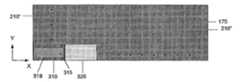
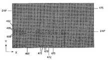
도 2는 샘플(170)의 반도체 박막(175)(예; 비정질 실리콘 박막) 및 상기 샘플(170) 상의 위치에 대해 빔 펄스(164)의 상대적 평행이동 경로에 대한 예시적 구현예를 확대한 도면이다. 이 예시적 샘플(170)은, 예를 들면, Y 방향으로 40cm 및 X 방향으로 30cm의 치수를 가진다. 샘플(170)은 소정 개수의 칼럼(예; 제1 개념상 칼럼(205), 제2 개념상 칼럼(206), 제3 개념상 칼럼(207) 등)으로 개념적으로 분할될 수 있다. 개념상 칼럼 각각의 위치/크기는 컴퓨터 장치(100)의 기억 장치에 저장되어, 추후에 샘플(170)의 평행이동 및/또는 반도체 박막(175)의 그러한 상대적 위치 또는 저장된 이치에 의거한 다른 위치에서의 빔 소스(110)에 의한 빔의 발사를 제어하는 데 활용될 수 있다. 개념상 칼럼(205, 206, 207, 등) 각각은, 예를 들면, Y 방향으로 1/2cm 및 X 방향으로 30cm의 치수를 갖는다. 따라서, 샘플(170)의 크기가 Y 방향으로 40cm일 경우, 샘플(150)은 개념적으로 80개의 칼럼으로 분할될 수 있다. 샘플(170)은 또한 개념적으로 다른 치수(예; 1cm×30cm 칼럼, 2cm×30cm 칼럼, 2cm×30cm 칼럼 등)를 가진 칼럼으로 분할될 수 있다. 사실상, 불균일성에 대한 염려 없이 TFT 장치의 적어도 활성 영역을 완전히 위치시킬 수 있도록 반도체 박막 샘플(175) 상에 균일한 영역을 형성하기 위해 상기 영역 내에 핵형성, 응고, 및 작은 그레인 성장을 촉진하는 데에 상기 칼럼에 있는 반도체 박막(175)의 특정 영역을 상기 빔 펄스(164)가 조사하여 완전히 용융시킬 수 있다면 샘플(170)의 개념상 칼럼의 치수에 대한 절대적인 제한은 없다. 칼럼 각각의 위치/치수 및 그의 위치는 컴퓨터 장치(100)의 기억 장치에 저장되어, 빔 펄스(164)에 대한 평행이동 스테이지(180)의 평행이동 및/또는 빔 소스(110)에 의한 빔(111)의 발사를 제어하기 위해 상기 컴퓨터 장치(100)에 의해 활용된다.2 is an enlarged view of an exemplary embodiment of a semiconductor thin film 175 (eg, an amorphous silicon thin film) of a
반도체 박막(175)은, 도 3에 도시된 바와 같이 본 발명의 제1 예시적 구현예에 따른 마스크(150)를 이용하여 패턴 형성되어 있는 빔 펄스(164)에 의해 조사될 수 있다. 제1 예시적 마스크(150)의 크기는 그 단면적이 상기 빔 펄스(164)의 단 면적보다 크도록 설정된다. 이와 같이 하여, 마스크(150)는 개구부 또는 마스크(150)의 투명 영역에 의해 유도되는 형상 및 프로파일을 갖도록 펄스형 빔의 패턴을 형성할 수 있다. 이 예시적 구현예에서, 마스크(150)는 빔-블록킹 섹션(155) 및 개구부 또는 투명 섹션(157)을 포함한다. 빔-블록킹 섹션(155)은 상기 섹션(155)에 충돌하는 펄스형 빔의 영역이 통과하여 조사되는 것을 막고, 그에 따라 도 1A에 도시된 본 발명의 예시적 시스템의 광이 샘플(170) 상에 제공된 반도체 박막(175)의 대응 영역을 조사하지 못하도록 더 이상의 진입을 막는다. 이와 대조적으로, 개구부 또는 투명 섹션(157)은 단면적이 상기 섹션(157)에 대응하는 빔 펄스(164)의 부분이 본 발명에 따른 시스템의 광이 진입하여 반도체 박막(175)의 대응 영역을 조사할 수 있게 한다. 이와 같이 하여, 마스크(150)는 이하에 보다 구체적으로 설명하는 바와 같이, 소정 부분에서 샘플(170)의 반도체 박막(175)을 충돌시키도록 빔 펄스(164)를 패터닝할 수 있다.As illustrated in FIG. 3, the semiconductor
본 발명에 따른 방법의 제1 예시적 구현예를 도 4A-4F에 도시된 바와 같이 샘플(170)의 반도체 박막(175)에 대한 조사를 참조하여 설명하기로 한다. 본 발명이 이 예시적 방법에서, 빔(111)은 도 3의 예시적 마스크(150)에 의해 형성되고, 샘플(170)의 반도체 박막(175)의 예시적 조사 및/또는 충돌은 도 2에 도시되어 있다. 예를 들면, 샘플(170)의 반도체 박막(175)의 선택된 영역을 조사하기 위해, 마스크(150) 또는 샘플 평행이동 스테이지(180)를 이동시킴으로써 샘플(170)을 빔 펄스(164)에 대해서 평행이동시킬 수 있다. 전술한 바를 위해, 레이저빔(149)의 길이와 폭은, 도 3의 마스크(150)에 의해 형성될 수 있도록 X 방향으로 1cm, Y 방 향으로 1/2cm(예; 직사각형)의 크기보다 더 클 수 있다. 그러나, 펄스형 레이저빔(149)은 상기 형상 및 크기에 한정되지 않음을 알아야 한다. 실제로, 당업자에게 공지되어 있는 바와 같이, 다른 형상 및/또는 크기의 레이저빔(149)을 얻을 수 있음은 물론이다(예; 정사각형, 삼각형, 원형 등).A first exemplary embodiment of the method according to the present invention will be described with reference to a survey of the semiconductor
개념상으로 샘플(170)이 여러 개의 칼럼(205, 206, 207, 등)으로 분할된 후, 펄스형 레이저빔(111)은 활성화되고(컴퓨터 장치(100)를 이용한 빔 소스(110)의 활성화 또는 셔터(130)의 개방에 의해), 반도체 박막(175)으로부터 이격한 제1 위치(220) 상에 충돌하는 펄스형 레이저 빔렛(164)을 생성한다. 이어서, 샘플(170)은 제1 빔 경로(225)에서 고정 위치의 빔렛에 대해 소정의 속도에 도달하도록 캄퓨터 장치(100)의 제어하에 전진하는 X 방향으로 평행이동되고 가속화된다.Conceptually, after the
본 발명의 방법의 변형예에서, 바람직하게 펄스형 레이저빔(149)에 대한 샘플(170)의 운동 속도가 소정의 속도에 도달할 때, 펄스형 빔렛(164)은 샘플(170)의 제1 에지(210')에 도달할 수 있다. 다음에, 샘플(170)은 소정의 속도를 갖고 연속적으로(즉, 정지하지 않고) -X 방향으로 평행이동하여, 펄스형 빔렛(164)은 제2 빔 경로(230)의 전장에 대해 샘플(170)의 후속되는 부분을 연속적으로 조사한다.In a variant of the method of the invention, preferably, when the speed of movement of the
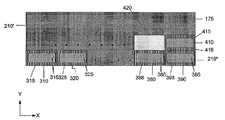
제1 에지(210')를 통과한 후, 빔 펄스(164)는, 바람직하게, 도 4A에 도시된 바와 같이, 해당 영역을 그 두께 전체에 걸쳐 완전히 용융시키는 충분한 세기로 반도체 박막(175)의 제1 영역(310)에 충돌하여 조사한다. 다음에, 도 4B에 도시된 바와 같이, 상기 제1 영역(310)은 응고 및 결정화가 이루어지고, 그 결과 상기 영역 내에 2개의 영역, 즉 제1 작은 그레인 영역(small-grained region)(315) 및 제1 횡방향 성장 영역(318)이 형성된다. 제1 작은 그레인 영역(315)은 제1 영역(310) 내 큰 섹션의 핵형성 후에 형성된다. 이 작은 그레인 영역(315)의 치수는 제1 영역(310)을 조사하는 빔 펄스(164)의 치수보다 약간 작고, 제1 작은 그레인 영역(315)은 제1 횡방향 성장 영역(318)에 의해 둘러싸인다(이에 대한 상세한 사항은 이하에 설명된다).After passing through the
제1 횡방향 성장 영역(318)은 반도체 박막(175)의 조사되지 않은 부분과 제1 조사 영역(310) 사이의 경계부로부터 그레인을 횡방향으로 성장시킴으로써 형성될 수 있다. 제1 작은 그레인 영역(318)의 그레인은 상기 경계부로부터 소정의 간격에 걸쳐 제1 용융 영역의 중심 방향으로 성장하여 제1 작은 그레인 영역(315)에 도달하고, 그 사이에 경계부를 형성한다. 이 소정의 간격은 제1 용융 영역(310)의 재응고 속도에 의해 제어된다. 예를 들면, 상기 소정의 간격은 1㎛ 내지 5㎛일 수 있다. 따라서, 제1 횡방향 성장 영역(318)은 그것이 둘러싸고 있는 제1 작은 그레인 영역(315)보다 훨씬 작다. 일반적으로, 사기 영역(315)의 그레인은 상기 영역(318)의 그레인보다 작다. 그러나, 제1 작은 그레인 영역(315)에 있는 작은 그레인 물질은 TFT 장치 및 적어도 TFT 장치의 활성 영역을 상기와 같은 균일한 작은 그레인 영역에 위치시킬 때 양호한 균일성을 제공한다. 본 발명의 목적을 위해, TFT 장치의 활성 영역을 그러한 작은 그레인 영역에 위치시키는 것은 바람직하지 않다.The first
이후에, 도 4C에 도시된 바와 같이, 샘플(170)은 계속해서 평행이동되어(또는 마스크(150)가 조절되도록 구성되어) 빔 펄스(164)는 반도체 박막(175)의 제2 영역(320)을 조사하여 완전히 용융시킨다(그의 두께 전체에 걸쳐). 여기서의 제2 영역(320)은 +X 방향을 따라 제1 개념상 칼럼(205)의 제1 영역(320)에 바로 이어지는 영역일 수 있다. 제1 영역(310)과 마찬가지로, 제2 영역(320)은 제2 작은 그레인 영역(325) 및 제2 횡방향 성장 영역(328) 내부로 재응고 및 결정화되며, 이들 영역은 각각 제1 작은 그레인 영역(315) 및 제1 횡방향 성장 영역(318)의 특징과 치수에 대응한다. 만일 제2 영역(320)을 조사하는 동안, 빔 펄스(164)가 제1 횡방향 성장 영역(318)에 약간 중첩되면, 재응고 시 이 영역(318)의 그레인은 제1 횡방향 성장 영역(318)에 바로 인접한 완전 용융된 제2 영역(320)의 일부분을 시드(seed)하여 횡방향으로 성장시킨다. 이러한 방식으로, 제2 횡방향 성장 영역(328)의 인접 섹션은 그로부터 그레인을 횡방향 성장시키도록 제1 횡방향 성장 영역(318)에 의해 시드된다. 얻어지는 결정화된 제2 영역(320)이 도 4D에 예시되어 있다. 제2 영역(320)이 결정화된 제1 영역(310)으로부터 소정의 간격을 두고 형성되도록 하는 것도 본 발명의 범위에 포함된다. 따라서, 결정화된 제1 횡방향 성장 영역(318)에 가장 가깝게 위치한 제2 횡방향 성장 영역(328)의 섹션은 제1 영역(310)과 제2 영역 사이의 조사되지 않은 섹션으로부터 그레인에 의해 시드된다.Subsequently, as shown in FIG. 4C, the
반도체 박막(175)의 제1 개념상 칼럼(205)에 대한 평행이동 및 조사는, 도 4E에 예시된 바와 같이, 상기 제1 개념상 칼럼(205)에서의 모든 영역(310, 320, …, 380, 390)(그리고 이들 각각의 작은 그레인 영역(315, 325, …, 385, 395) 및 횡방향 성장 영역(318, 328, …, 388, 398))이 계속되어 펄스형 빔렛(164)이 샘플(170)의 제2 에지(210")에 도달할 때까지 계속된다. 제1 개념상 칼럼(205)을 따른 영역(310, 320, …, 380, 390)의 결정화는 실질적으로 반복되는 방식으로 실행된다. 빔 펄스(164)가 제2 에지(210")를 통과할 때, 샘플(170)의 평행이동은 빔 펄스(164)(제3 빔 펄스(235)에서의)에 대해 느려져서 제2 위치(240)에 도달할 수 있다(도 2 참조). 빔 펄스(164)가 샘플(170)의 제2 에지(210")를 가로지른 후에는 더 이상 샘플(170)을 조사하지 않기 때문에 펄스형 빔(111)을 차단할 필요가 없음을 알아야 한다.The translation and irradiation of the first
샘플(170)과 제2 에지(210")로부터 떨어져 있는 상태로, 샘플은 제4 빔 경로(245)를 통해 제3 위치(247)를 향해 -Y 방향으로 평행이동되어 제2 개념상 칼럼(206)을 따라 반도체 박막(175)의 섹션을 조사할 수 있게 된다. 이어서, 샘플(170)이 제3 위치(247)로 평행이동되었을 때 발생될 수 있는 샘플(170)의 모든 진동이 멈추어지도록 샘플(170)을 상기 위치(247)에 자리잡게 한다. 샘플(170)이 제2 개념상 칼럼(206)에 도달하려면, 1/2cm의 폭(-Y 방향)을 가진 칼럼의 경우에 약 1/2cm 평행이동된다. 다음에, 빔 펄스(164)에 의한 반도체 박막(175)에 대한 충돌이 도달하고 나서 제2 에지(210")를 바이패스하도록, 샘플(170)은 -X 방향으로 제4 빔 경로(250)를 통해 소정의 속도로 가속된다.Apart from the
그 후, 샘플(170)은 제5 빔 경로(255)를 따라 평행이동되고, 샘플을 +X 방향으로 평행이동하는 상태에서 추가적 영역(410, 420), 그들 각각의 작은 그레인 영역(415, 425) 및 횡방향 성장 영역(418, 428)을 조사하기 위해, 제1 칼럼(205)의 조사에 관해 전술한 예시적 공정이 제2 개념상 칼럼(206)에 대해 반복될 수 있다. 이 방식으로, 샘플(170)의 모든 개념상 칼럼이 조사된다. 또한, 빔 펄스(164)가 제1 에지(210')에 도달하면, 샘플(170)의 평행이동은 제6 빔 경로(260)를 따라 감속되어 제4 위치(265)에 도달한다. 이 지점에서 샘플(170)은 빔 펄스가 샘플(170)의 테두리 외부에 있도록 제7 빔 경로(270)를 따라 -Y 방향으로 평행이동되어 제5 위치(272)에 도달하고, 샘플(170)로부터 모든 진동이 멈추어지도록 샘플(170)의 평행이동은 정지된다. 그 후, 빔 펄스(164)가 샘플(170)의 제1 에지(210')에 도달하여 통과하도록 -X 방향으로 제8 빔 경로(275)를 따라 가속되고, 빔 펄스(164)는 제3 개념상 칼럼(207)의 특정 영역을 조사하고 완전히 용해시킴으로써, 제1 개념상 칼럼(205)의 영역(310, 320, …, 380, 390) 및 제2 개념상 칼럼(206)의 영역(410, 420, …)에 대해 전술한 바와 실질적으로 동일한 방식으로 상기 영역이 결정화될 수 있다.Thereafter, the
이러한 과정은 반도체 박막(175)의 모든 개념상 칼럼, 및 개념적으로 칼럼으로 분할되지 않아도 되는 박막(175)의 특정 섹션의 선택적 칼럼에 대해 반복될 수 있다. 또한, 컴퓨터 장치(100)의 기억 장치에 저장되어 있는 미리 정의된 위치를 기초로 하여 컴퓨터 장치(100)는 빔 소스(110)에 의한 빔(111)의 발사를 제어할 수 있다(예를 들면, 반도체 박막(175)을 조사하는 대신에 펄스 지속시간을 설정함으로써). 예를 들면, 컴퓨터 장치(100)는 빔(111)을 생성하도록 빔 소스(110)를 제어하여 그에 대응하는 빔 펄스(164)로 박막(175)의 특정 영역의 소정 위치만을 조사함으로써, 컴퓨터 장치(100)에 의해 이들 위치가 기억되어 샘플(170)이 빔 펄스(164)의 경로에서 직접 상기 영역에 위치하도록 평행이동될 때에만 빔 펄스에 의한 조사를 이루어내는 빔(111)의 발사를 개시하는 데 이용된다. 빔 소스(110)는 X 방 향에서의 위치 좌표에 의거하여 컴퓨터 장치(100)를 통해 발사될 수 있다.This process may be repeated for all conceptual columns of the semiconductor
또한, 용융시키고 결정화할 반도체 박막(175)의 영역을 빔 펄스(164)의 조사 경로가 지향하고 있을 때, 반드시 연속적이 아니어도 되는 방식으로 샘플(170)을 평행이동할 수 있다. 따라서, 샘플(170)의 평행이동은 샘플(170)의 중간에서 정지시킬 수 있고, 중간 영역이 조사되고, 완전히 용융되고, 이어서 재응고 및 결정화된다. 그 후, 샘플(170)은 반도체 박막(175)의 다른 섹션이 빔 펄스(164)의 경로에 배열되도록 이동됨으로써, 샘플의 평행이동은 다시 정지되고, 앞에서 구체적으로 설명한 방법의 예시적 구현예 및 이하에서 설명하게 되는 방법의 구현예에 따라 특정 섹션이 조사되어 완전히 용융된다.In addition, when the irradiation path of the
본 발명에 따르면, 여기에 설명되고 제시된 마스크 및 '535출원에 설명되고 예시된 마스크는 어느 것이나 본 발명에 따른 방법 및 시스템에 이용할 수 있다. 예를 들면, 반도체 박막(175)을 투광 조사(flood-irradiation)시키는 도 3에 도시된 마스크를 이용하는 대신에 도 5A에 도시된 마스크(150')의 제2 예시적 구현예를 활용할 수 있다. 개구부 또는 투명 영역(157)이 1개인 도 3의 마스크(150)와 대조적으로, 상기 마스크(150')는 빔 블록킹 영역(455)에 의해 서로 분리되어 있는 복수의 개구부 또는 투명 영역(450)을 가진다. 마스크(150')의 개구부 또는 투명 영역(450)은 "슬릿"이라고도 지칭된다. 이들 슬릿은 작은 빔 펄스(또는 빔렛)를 통과시켜 조사하여 펄스가 충돌하는 반도체 박막(175)의 영역을 완전히 용융시킬 수 있게 한다. 슬릿(450) 중 하나를 확대한 것이 도 5B에 예시되어 있는데, 여기서 슬릿(450)의 치수는 0.5㎛×0.5㎛일 수 있음을 나타낸다. 슬릿의 다른 치수도 가 능하며, 그러한 치수도 본 발명의 범위에 포함됨을 명확히 이해해야 할 것이다. 예컨대, 슬릿은 직사각형, 원형, 삼각형, 셰브론(chevron) 형상, 다이아몬드 형상 등을 가질 수 있다.According to the present invention, any of the masks described and presented herein and the masks described and illustrated in the '535 application may be used in the methods and systems according to the present invention. For example, instead of using the mask shown in FIG. 3 for flood-irradiating the semiconductor
도 6A-6D는 본 발명에 따른 제2 구현예의 진행을 예시하는 도면으로서, 반도체 박막(175)의 제1 개념상 칼럼(205)을 따라 복수의 연속된 영역이 도 5A의 마스크(150')에 의해 형성된 빔 펄스(164)(빔렛으로 이루어짐)에 의해 조사된다. 빔 펄스(164)에 의한 충돌에 대해 샘플(170)의 평행이동은 도 4A-4F를 참조하여 앞에서 설명한 평행이동과 실질적으로 동일하다. 도 3의 마스크(150)에 의해 형성된 빔 펄스(164)에 의한 영역(310, 320, …, 380, 390, 410, 420)의 조사와, 마스크(150')에 의해 형성된 빔 펄스(164)에 의한 영역(460, 470)의 조사 사이의 차이점은, 실질적으로 상기 영역(310, 320, …, 380, 390, 410, 420) 전체가 조사되어 완전 용융되는 것에 반하여 상기 영역(460, 470)의 특정한 작은 부분(462)만이 조사되어 그 두께 전체에 걸쳐 완전 용융되는 것이다.6A-6D illustrate the progress of a second embodiment in accordance with the present invention, wherein a plurality of contiguous regions along the first
도 4A의 영역(310)과 유사하게, 영역(460)의 부분(462)은 도 6A에 도시된 바와 같이 조사되어 완전 용융된다. 그 후, 상기 부분(462)은 재응고되어 도 4B에 도시된 바와 같이 작은 그레인 영역(465)(핵형성에 기인함) 및 횡방향 성장 영역(468)을 형성한다. 제1 작은 그레인 영역(315)과 유사하게, 각 부분(462)의 작은 그레인 영역(465)은 그 안에 작은 그레인 균일 물질을 가지며, TFT 장치의 적어도 활성 영역(아울러 전체 TFT 장치도 가능함)이 각각의 상기 영역(465) 내에 배치될 수 있는 크기를 갖는다. 상기 영역(465)의 작은 그레인 균일 물질은 이 영역의 핵 형성 및 재응고로 인해 형성된다. 도 6C에 도시된 바와 같이, 샘플(170)이 -X 방향으로 평행이동되면, 영역(470)의 부분(472)은 조사되어, 부분(462)과 실질적으로 동일한 방식으로 완전 용융된다. 이러한 방식으로, 작은 그레인 영역(475) 및 영역(470)의 횡방향 성장 영역(478)이 형성된다.Similar to
또한, 도 7에 도시된 바와 같이 본 발명에 따른 마스크(150")의 제3 구현예를 활용할 수 있는바, 상기 마스크(150")는 빔(149)을 빔 펄스(164)로 패턴하고 성형하기 위한 길고 좁은 개구부 또는 투명 영역(490)을 가진다. 예를 들면, 영역(490)의 길이는 0.5cm이고 폭은 0.1mm일 수 있다. 이 방식으로, 도 2에 도시된 샘플(170)의 개념상 칼럼 각각은 마스크(150")에 의해 성형된 빔 펄스(164)에 의해 조사될 수 있다. 또한, 영역(490)의 길이를 30cm로 할 수 있다. 이에 따라, 반도체 박막(175)을 소정 수의 개념상 칼럼으로 분할하여 각 칼럼을 개별적으로 조사하는 대신에, 샘플(170)을 -Y 방향으로, 샘플(170)의 한 에지로부터 그 반대측 에지로 평행이동함으로써 반도체 박막(175)의 선택된 부분을 조사하여 완전히 용융시킬 수 있다. 중요한 것은 각각의 TFT 장치의 활성 영역을 위치시킬 수 있도록 상기 공정 기법을 이용하여 작은 그레인 균일 영역을 형성하는 것이다.In addition, as shown in FIG. 7, a third embodiment of the
도 8A는, 도 4D의 제1 및 제2 영역(310, 320) 및/또는 도 6D의 영역(460)의 인접 부분(462)에 대응할 수 있는, 제1 및 제2의 조사되고 재응고되어 결정화된 영역(510, 520)을 예시한다. 특히 도 8A는 전체적인 TFT 장치(610, 620)가 영역(510, 520)의 각각의 균일한 작은 그레인 영역(515, 525) 내에 위치할 수 있음을 나타낸다. 영역(510)의 작은 그레인 영역(515)에 위치한 제1 TFT 장치(610)는 게이트(612), 드레인(614), 소스(616) 및 활성 영역(618)을 포함하고, 이들 모두는 횡방향 성장 영역(518)으로부터 거리를 두고 제공된다. 마찬가지로, 제2 TFT 장치(610)에 있어서, 그의 게이트(622), 드레인(624), 소스(626), 및 특히 활성 영역(628)도 상기 영역(520)의 각각의 횡방향 성장 영역(528)과 중첩되지 않는다.FIG. 8A is first and second irradiated and resolidified, which may correspond to the first and
도 8B는 각각의 TFT 장치(610, 620')가 그 위에 제공되어 있는, 도 6D의 영역(460)의 인접 부분(462)에 대응할 수도 있는 제1 및 제2의 조사되고 재응고되어 결정화된 영역(510, 520)을 예시한다. 이 예시적 구현예에서, 영역(510, 520)의 각각의 활성 영역(618', 620')만이 영역(510, 520)의 각각의 균일한 작은 그레인 영역(515, 525) 내에 제공되는 한편, TFT 장치(610', 620')의 다른 부분은 영역(510, 520)의 각각의 횡방향 성장 영역(518, 528) 상에 위치한다. 특히, 제1 TFT 장치(610')는 완전히 영역(510)의 작은 그레인 영역(515)에 위치하는 활성 영역(618')을 포함하는 한편, TFT 장치(610')의 게이트(612'), 드레인(614') 및 소스(616')는 횡방향 성장 영역(518)과 중첩된다. 또한, 제2 TFT 장치(610')에 있어서, 활성 영역(628')은 완전히 영역(520)의 각각의 작은 그레인 영역(525) 내에 위치하는 한편, 제2 TFT 장치(620')의 게이트(622'), 드레인(624') 및 소스(626)는 영역(520)의 각각의 횡방향 성장 영역(528) 상에 제공되어 있다. 또한, 게이트(622')는 영역(510)의 작은 그레인 영역(515)과 영역(520)의 작은 그레인 영역(525) 사이의 경계 영역(500) 상에 제공된다. 게이트(612, 612', 622, 622'), 드레인(614, 614', 624, 624) 및 소스(616, 616', 626, 626') 중 어느 하나는 횡방향 성장 영역(518, 528) 및 경계 영역(500) 상에 제공될 수 있음을 이해해야 한다. 이에 더하여, 본 발명의 또 다른 구현예에 따르면, 각각의 TFT 장치(610', 620')의 활성 영역(618', 628')의 작은 부분을 경계 영역(500) 또는 횡방향 성장 영역(518, 528) 상에 위치시킬 수 있는 한편, 이들 활성 영역(618', 628')의 주요 부분이 작은 그레인 영역(515, 525) 내에 제공되도록 할 수 있다.FIG. 8B illustrates first and second irradiated and resolidified crystallized crystals that may correspond to
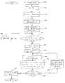
도 9는 도 4A-4F 및 도 6A-6D에 예시한 본 발명의 기술을 이용하여 도 1A의 컴퓨터 장치의 적어도 부분적 제어 하에 본 발명의 제1 예시적 처리 방법을 나타내는 흐름도이다. 단계 1000에서, 빔 소스(110), 에너지 빔 변조기(120), 빔 감쇠기 및 셔터(130)와 같은 도 1A에 나타낸 시스템의 하드웨어 부재를 적어도 부분적으로 컴퓨터 장치(100)를 이용하여 우선 초기화한다. 단계 1005에서 샘플(170)이 샘플 평행이동 스테이지(1800) 상에 로딩된다. 상기 로딩은 컴퓨터 장치(100)의 제어 하에 공지된 샘플 로딩 장치를 이용하여 수동식 또는 자동식으로 실행할 수 있음을 알아야 한다. 다음에, 단계 1010에서, 바람직하게는 컴퓨터 장치(100)의 제어 하에, 샘플 평행이동 스테이지(180)를 초기 위치로 이동시킨다. 필요할 경우, 단계 1015에서, 적절한 포커스 및 정렬을 위해, 시스템의 여러 가지 다른 광학적 구성요소를 수동식으로 또는 컴퓨터 장치(100)의 제어 하에 조절 및/또는 정렬한다. 단계 1020에서, 조사/레이저 빔(111)을 소정의 펄스 에너지 레벨, 펄스 지속시간 및 반복률로 안정화시킨다. 단계 1024에서, 각각의 빔 펄스가 반도체 박막(175)의 조사된 부분을 과용융(over-melting)하지 않고 완전 용융시키기에 충분한 에너지를 갖고 있는지 여부를 바람직하게 판정한다. 에너지가 충분하지 않을 경우, 단계 1025에서 컴퓨터 장치(100)의 제어 하에 빔 소스(110)에 의해 빔(111)의 감쇠를 조절하고, 반도체 박막의 부분을 용융하기에 충분한 에너지가 있는지를 판정하기 위해 단계 1024를 다시 실행한다.9 is a flow diagram illustrating a first exemplary processing method of the present invention under at least partial control of the computer device of FIG. 1A using the techniques of the present invention illustrated in FIGS. 4A-4F and 6A-6D. In
단계 1027에서, 빔 펄스(164)를 반도체 박막의 제1 칼럼에 충돌시키는 방향을 지향하도록 샘플(170)을 위치시킨다. 이어서, 단계 1030에서, 마스킹된 세기 패턴 또는 성형된 빔 펄스를 이용하여(예; 마스크(150)를 이용하거나 단순히 빔을 성형하여) 반도체 박막의 부분을 조사하고 그 전체 두께에 걸쳐 완전히 용융시킨다. 그 후, 반도체 박막이 조사된 부분이 응고되고 결정화됨으로써, 응고된 부분의 특정 영역이 핵형성되고 균일한 물질을 내포하도록 하여, TFT 장치의 적어도 활성 영역을 내부에 완전히 위치시킬 수 있도록 한다. 단계 1035에서, 빔 펄스에 의한 현재의 개념상 칼럼에 대한 조사가 완결되었는지 여부를 판정한다. 완결되지 않았을 경우, 단계 1045에서, 샘플은 다음번 빔 펄스(164)로 계속 조사된다. 그러나, 단계 1035에서 현재의 개념상 칼럼에 대한 조사 및 결정화가 완결되었다고 판정되면, 단계 1045에서 처리해야할 샘플(170)의 개념상 칼럼이 더 있는지 여부를 판정한다. 더 있을 경우, 공정은 단계 1050으로 계속되는데, 여기서는 본 발명에 따라 처리될 다음번 칼럼에 빔 펄스를 지향하도록 샘플은 평행이동된다. 그렇지 않으면, 단계 1055에서, 예시적 처리는 샘플(170)에 대해 완료되었으며, 도 1A에 도시된 시스템의 하드웨어 부재 및 빔(111)은 차단되고, 공정은 종료된다.In
도 10은, 바람직하게 반도체 박막(175) 상의 사전 지정된 위치를 기초로 샘플(170)을 조사하는 방법인, 도 4A-4F 및 도 6A-6D에 예시한 본 발명의 기술을 이 용하여 도 1A의 컴퓨터 장치의 적어도 부분적 제어 하에 본 발명의 제2 예시적 처리 방법을 나타내는 흐름도이다. 이 예시적 방법의 단계 1100-1120은 도 9의 방법에서의 단계 1000-1-2-과 실질적으로 동일하므로, 여기에서 더 구체적으로 설명하지 않는다. 그러나, 단계 1024에서, 조사된 부분이 결정화하도록 적어도 반도체 박막(175)의 부분을 조사하는 충분한 에너지를 각 빔(111)이 갖고 있는지 여부를 판정한다. 충분하지 않을 경우, 단계 1125에서, 빔 펄스에 대한 감쇠를 조절하고, 에너지 플루언스를 다시 검증한다. 빔 펄스의 에너지 플루언스가 검증되면, 샘플은 샘플(170)의 제1 칼럼을 충돌시키도록 이동된다.10 illustrates the method of FIG. 1A using the techniques of the invention illustrated in FIGS. 4A-4F and 6A-6D, which are preferably methods of irradiating the
다음에, 단계 1130에서, 얻어지는 빔(149)을 마스크(159)를 통과시켜 빔 펄스를 성형하고, 얻어지는 펄스의 에지 부분을 성형한다. 이어서, 단계 1135에서, 현재의 칼럼을 따라 샘플(170)을 연속적으로 평행이동시킨다. 단계 1140에서, 샘플(170)을 평행이동시키는 동안, 조사된 부분이 결정화되도록, 예를 들면, 마스킹된 세기 패턴 빔 펄스를 이용하여 반도체 박막의 부분을 조사하여, 그 전체 두께에 걸쳐 완전히 용융시킨다. 이러한 반도체 박막(175)의 부분에 대한 조사는 빔 펄스(164)가 샘플(170)의 특정 위치에 도달할 때 실행될 수 있고, 상기 위치는 컴퓨터 장치(100)에 의해 사전 지정고 컴퓨터 장치의 기억 장치에 저장되어 있는 것이다. 이와 같이, 빔 소스(110)는 빔 펄스(164)에 대한 이들 위치에 도달하는 샘플(170)에 발사될 수 있다. 그 후, 응고된 부분의 특정 영역에 핵형성이 이루어지고, TFT 장치의 활성 영역이 거기에 위치하도록 균일한 물질을 포함하도록 반도체 박막(175)의 조사된 부분을 응고시키고 결정화한다. 상기 공정은 반도체 박막(175)(예 들 들면, 샘플(170)의 에지) 상의 현재의 개념상 칼럼의 말단부가 도달될 때까지 계속된다. 단계 1145에서, 처리해야 하는 샘플(170)의 개념상 칼럼이 더 있는지 여부를 판정한다. 더 있는 경우, 공정은 단계 1150으로 이행되어 여기서 빔 펄스(164)가 본 발명에 따라 처리할 다음번 개념상 칼럼을 지향하도록 샘플을 평행이동한다. 그렇지 않으면, 단계 1155가 실행되는데, 이 단계는 도 9의 단계 1055와 실질적으로 동일하다.Next, in
이상이 설명은 본 발명의 원리를 예시하는 것일 뿐이다. 본 명세서에 교시된 내용을 참조하여 당업자에게는 전술한 구현예에 대한 다양한 변형 및 변경이 명백할 것이다. 예를 들면, 전술한 구현예가 반도체 박막의 적어도 부분적 횡방향 응고 및 결정화에 관하여 설명되었지만, 이는 국제특허 출원번호 PCT/US01/12799 및 미국특허 출원번호 09/390,535, 09/390/537 및 09/526,585(이들의 모든 개시 내용은 원용에 의해 본 명세서에 포함됨)에 기재되어 있는 것을 포함하여, 마이크로 가공(micro-machining), 포토-애블레이션(photo-ablation) 및 마이크로 패터닝(micro-patterning) 기술과 같은 그 밖의 물질 처리 기술에 적용될 수 있다. 전술한 인용 특허 문헌에 기재된 다양한 마스크 패턴 및 세기 빔 패턴은 본 발명의 방법 및 시스템과 함께 활용될 수 있다. 전술한 시스템 및 방법이, 예를 들면, 반도체 박막을 처리하는 것에 결부되어 있지만, 이러한 기술 및 시스템은 금속 박막 등을 포함하는 다른 필름을 처리하는 데에도 이용될 수 있음을 이해해야 할 것이다.The foregoing description merely illustrates the principles of the present invention. Various modifications and variations to the embodiments described above will be apparent to those skilled in the art with reference to the teachings herein. For example, while the foregoing embodiments have been described with respect to at least partial lateral solidification and crystallization of semiconductor thin films, they are described in International Patent Application Nos. PCT / US01 / 12799 and US Patent Application Nos. 09 / 390,535, 09/390/537 and 09 /. Micro-machining, photo-ablation and micro-patterning techniques, including those described in 526,585 (all of which are incorporated herein by reference) It can be applied to other material processing techniques such as. Various mask patterns and intensity beam patterns described in the above cited patent documents can be utilized with the methods and systems of the present invention. While the systems and methods described above are associated with processing semiconductor thin films, for example, it will be appreciated that such techniques and systems can also be used to process other films including metal thin films and the like.
따라서 당업자는, 본 명세서에 명시적으로 제시되거나 설명되어 있지 않더라도, 본 발명의 원리를 구현하는 여러 가지 시스템과 방법을 안출할 수 있을 것이 며, 이는 본 발명의 사상 및 범위에 포함된다.Therefore, those skilled in the art will be able to devise various systems and methods for implementing the principles of the present invention, even if not explicitly set forth or described herein, which are included in the spirit and scope of the present invention.
Claims (104)
Translated fromKoreanApplications Claiming Priority (3)
| Application Number | Priority Date | Filing Date | Title |
|---|---|---|---|
| US40508402P | 2002-08-19 | 2002-08-19 | |
| US60/405,084 | 2002-08-19 | ||
| PCT/US2003/025946WO2004017379A2 (en) | 2002-08-19 | 2003-08-19 | Process and system for processing a thin film sample and thin film structure |
Publications (2)
| Publication Number | Publication Date |
|---|---|
| KR20050052477A KR20050052477A (en) | 2005-06-02 |
| KR101118974B1true KR101118974B1 (en) | 2012-03-15 |
Family
ID=31888393
Family Applications (1)
| Application Number | Title | Priority Date | Filing Date |
|---|---|---|---|
| KR1020057002863AExpired - Fee RelatedKR101118974B1 (en) | 2002-08-19 | 2003-08-19 | Process and system for laser crystallization processing of film regions on a substrate to provide substantial uniformity, and a structure of such film regions |
Country Status (7)
| Country | Link |
|---|---|
| US (1) | US7259081B2 (en) |
| JP (1) | JP4879486B2 (en) |
| KR (1) | KR101118974B1 (en) |
| CN (1) | CN100447941C (en) |
| AU (1) | AU2003258288A1 (en) |
| TW (1) | TWI325157B (en) |
| WO (1) | WO2004017379A2 (en) |
Families Citing this family (50)
| Publication number | Priority date | Publication date | Assignee | Title |
|---|---|---|---|---|
| US6555449B1 (en) | 1996-05-28 | 2003-04-29 | Trustees Of Columbia University In The City Of New York | Methods for producing uniform large-grained and grain boundary location manipulated polycrystalline thin film semiconductors using sequential lateral solidfication |
| US6830993B1 (en) | 2000-03-21 | 2004-12-14 | The Trustees Of Columbia University In The City Of New York | Surface planarization of thin silicon films during and after processing by the sequential lateral solidification method |
| KR100854834B1 (en) | 2000-10-10 | 2008-08-27 | 더 트러스티스 오브 컬럼비아 유니버시티 인 더 시티 오브 뉴욕 | Method and apparatus for processing thin metal layers |
| US6961117B2 (en) | 2000-11-27 | 2005-11-01 | The Trustees Of Columbia University In The City Of New York | Process and mask projection system for laser crystallization processing of semiconductor film regions on a substrate |
| KR100400510B1 (en)* | 2000-12-28 | 2003-10-08 | 엘지.필립스 엘시디 주식회사 | A machine for Si crystallization and method of crystallizing Si |
| TW556350B (en) | 2001-08-27 | 2003-10-01 | Univ Columbia | A method to increase device-to-device uniformity for polycrystalline thin-film transistors by deliberately mis-aligning the microstructure relative to the channel region |
| AU2003220611A1 (en) | 2002-04-01 | 2003-10-20 | The Trustees Of Columbia University In The City Of New York | Method and system for providing a thin film |
| WO2004017380A2 (en) | 2002-08-19 | 2004-02-26 | The Trustees Of Columbia University In The City Of New York | A single-shot semiconductor processing system and method having various irradiation patterns |
| CN100447941C (en) | 2002-08-19 | 2008-12-31 | 纽约市哥伦比亚大学托管会 | A method and system for processing thin film samples and its thin film domain structure |
| US7300858B2 (en) | 2002-08-19 | 2007-11-27 | The Trustees Of Columbia University In The City Of New York | Laser crystallization and selective patterning using multiple beamlets |
| KR101131040B1 (en) | 2002-08-19 | 2012-03-30 | 더 트러스티스 오브 콜롬비아 유니버시티 인 더 시티 오브 뉴욕 | Process and system for laser crystallization processing of film regions on a substrate to minimize edge areas, and structure of such film regions |
| WO2004075263A2 (en) | 2003-02-19 | 2004-09-02 | The Trustees Of Columbia University In The City Of New York | System and process for processing a plurality of semiconductor thin films which are crystallized using sequential lateral solidification techniques |
| KR100997275B1 (en)* | 2003-06-12 | 2010-11-29 | 엘지디스플레이 주식회사 | Silicon Crystallization Method |
| US8441049B2 (en) | 2003-07-16 | 2013-05-14 | Samsung Display Co., Ltd. | Flat panel display device comprising polysilicon thin film transistor and method of manufacturing the same |
| US7164152B2 (en) | 2003-09-16 | 2007-01-16 | The Trustees Of Columbia University In The City Of New York | Laser-irradiated thin films having variable thickness |
| WO2005029546A2 (en) | 2003-09-16 | 2005-03-31 | The Trustees Of Columbia University In The City Of New York | Method and system for providing a continuous motion sequential lateral solidification for reducing or eliminating artifacts, and a mask for facilitating such artifact reduction/elimination |
| TWI351713B (en) | 2003-09-16 | 2011-11-01 | Univ Columbia | Method and system for providing a single-scan, con |
| TWI359441B (en) | 2003-09-16 | 2012-03-01 | Univ Columbia | Processes and systems for laser crystallization pr |
| US7318866B2 (en) | 2003-09-16 | 2008-01-15 | The Trustees Of Columbia University In The City Of New York | Systems and methods for inducing crystallization of thin films using multiple optical paths |
| US7364952B2 (en) | 2003-09-16 | 2008-04-29 | The Trustees Of Columbia University In The City Of New York | Systems and methods for processing thin films |
| WO2005029547A2 (en) | 2003-09-16 | 2005-03-31 | The Trustees Of Columbia University In The City Of New York | Enhancing the width of polycrystalline grains with mask |
| WO2005034193A2 (en) | 2003-09-19 | 2005-04-14 | The Trustees Of Columbia University In The City Ofnew York | Single scan irradiation for crystallization of thin films |
| EP1728271B1 (en) | 2004-03-26 | 2016-06-08 | Semiconductor Energy Laboratory Co, Ltd. | Laser irradiation method and laser irradiation apparatus |
| US8525075B2 (en)* | 2004-05-06 | 2013-09-03 | Semiconductor Energy Laboratory Co., Ltd. | Laser irradiation apparatus |
| US7566602B2 (en)* | 2004-06-12 | 2009-07-28 | Samsung Electronics Co., Ltd. | Methods of forming single crystalline layers and methods of manufacturing semiconductor devices having such layers |
| KR100578787B1 (en)* | 2004-06-12 | 2006-05-11 | 삼성전자주식회사 | Semiconductor device and manufacturing method thereof |
| CN100530549C (en)* | 2004-08-23 | 2009-08-19 | 株式会社半导体能源研究所 | Laser irradiation apparatus, irradiation method, and method of manufacturing semiconductor device |
| US20060189091A1 (en)* | 2004-11-11 | 2006-08-24 | Bo Gu | Method and system for laser hard marking |
| US7645337B2 (en) | 2004-11-18 | 2010-01-12 | The Trustees Of Columbia University In The City Of New York | Systems and methods for creating crystallographic-orientation controlled poly-silicon films |
| US8221544B2 (en) | 2005-04-06 | 2012-07-17 | The Trustees Of Columbia University In The City Of New York | Line scan sequential lateral solidification of thin films |
| KR101284201B1 (en)* | 2005-05-02 | 2013-07-09 | 가부시키가이샤 한도오따이 에네루기 켄큐쇼 | Laser irradiation apparatus and laser irradiation method |
| US8598588B2 (en) | 2005-12-05 | 2013-12-03 | The Trustees Of Columbia University In The City Of New York | Systems and methods for processing a film, and thin films |
| US20080030877A1 (en)* | 2006-08-07 | 2008-02-07 | Tcz Gmbh | Systems and methods for optimizing the crystallization of amorphous silicon |
| TW200942935A (en) | 2007-09-21 | 2009-10-16 | Univ Columbia | Collections of laterally crystallized semiconductor islands for use in thin film transistors and systems and methods for making same |
| JP5385289B2 (en) | 2007-09-25 | 2014-01-08 | ザ トラスティーズ オブ コロンビア ユニヴァーシティ イン ザ シティ オブ ニューヨーク | Method for producing high uniformity in thin film transistor devices fabricated on laterally crystallized thin films |
| WO2009067687A1 (en) | 2007-11-21 | 2009-05-28 | The Trustees Of Columbia University In The City Of New York | Systems and methods for preparation of epitaxially textured thick films |
| US8012861B2 (en) | 2007-11-21 | 2011-09-06 | The Trustees Of Columbia University In The City Of New York | Systems and methods for preparing epitaxially textured polycrystalline films |
| WO2009067688A1 (en) | 2007-11-21 | 2009-05-28 | The Trustees Of Columbia University In The City Of New York | Systems and methods for preparing epitaxially textured polycrystalline films |
| US8569155B2 (en) | 2008-02-29 | 2013-10-29 | The Trustees Of Columbia University In The City Of New York | Flash lamp annealing crystallization for large area thin films |
| JP2012508985A (en) | 2008-11-14 | 2012-04-12 | ザ トラスティーズ オブ コロンビア ユニヴァーシティ イン ザ シティ オブ ニューヨーク | System and method for thin film crystallization |
| KR101259982B1 (en)* | 2009-09-25 | 2013-06-03 | (주)티엔스 | micromachining system using excimer laser beam and control method thereof |
| US9646831B2 (en) | 2009-11-03 | 2017-05-09 | The Trustees Of Columbia University In The City Of New York | Advanced excimer laser annealing for thin films |
| US9087696B2 (en) | 2009-11-03 | 2015-07-21 | The Trustees Of Columbia University In The City Of New York | Systems and methods for non-periodic pulse partial melt film processing |
| US8440581B2 (en) | 2009-11-24 | 2013-05-14 | The Trustees Of Columbia University In The City Of New York | Systems and methods for non-periodic pulse sequential lateral solidification |
| JP5534402B2 (en) | 2009-11-05 | 2014-07-02 | 株式会社ブイ・テクノロジー | Low temperature polysilicon film forming apparatus and method |
| KR101666661B1 (en)* | 2010-08-26 | 2016-10-17 | 삼성디스플레이 주식회사 | Thin film transistor substrate and flat panel display apparatus |
| US20140015170A1 (en)* | 2012-07-10 | 2014-01-16 | Electro Scientific Industries, Inc. | Method and apparatus for marking an article |
| FR3004848B1 (en)* | 2013-04-22 | 2015-06-05 | Centre Nat Rech Scient | METHOD OF MODIFYING THE VALUE OF AN ELECTRIC RESISTANCE COMPRISING A FERROMAGNETIC MATERIAL |
| US10629434B2 (en) | 2015-04-08 | 2020-04-21 | The Trustees Of Columbia University In The City Of New York | Laser irradiation induced surface planarization of polycrystalline silicon films |
| TWI850014B (en)* | 2019-04-05 | 2024-07-21 | 日商東京威力科創股份有限公司 | Substrate processing system |
Citations (1)
| Publication number | Priority date | Publication date | Assignee | Title |
|---|---|---|---|---|
| US6368945B1 (en) | 2000-03-16 | 2002-04-09 | The Trustees Of Columbia University In The City Of New York | Method and system for providing a continuous motion sequential lateral solidification |
Family Cites Families (103)
| Publication number | Priority date | Publication date | Assignee | Title |
|---|---|---|---|---|
| FR2030468A5 (en)* | 1969-01-29 | 1970-11-13 | Thomson Brandt Csf | |
| US4234358A (en)* | 1979-04-05 | 1980-11-18 | Western Electric Company, Inc. | Patterned epitaxial regrowth using overlapping pulsed irradiation |
| US4309225A (en)* | 1979-09-13 | 1982-01-05 | Massachusetts Institute Of Technology | Method of crystallizing amorphous material with a moving energy beam |
| EP0191503A3 (en)* | 1980-04-10 | 1986-09-10 | Massachusetts Institute Of Technology | Method of producing sheets of crystalline material |
| US4382658A (en)* | 1980-11-24 | 1983-05-10 | Hughes Aircraft Company | Use of polysilicon for smoothing of liquid crystal MOS displays |
| US4456371A (en)* | 1982-06-30 | 1984-06-26 | International Business Machines Corporation | Optical projection printing threshold leveling arrangement |
| US4691983A (en)* | 1983-10-14 | 1987-09-08 | Hitachi, Ltd. | Optical waveguide and method for making the same |
| US4639277A (en)* | 1984-07-02 | 1987-01-27 | Eastman Kodak Company | Semiconductor material on a substrate, said substrate comprising, in order, a layer of organic polymer, a layer of metal or metal alloy and a layer of dielectric material |
| JPH0433327Y2 (en) | 1985-04-19 | 1992-08-10 | ||
| JPH084067B2 (en)* | 1985-10-07 | 1996-01-17 | 工業技術院長 | Method for manufacturing semiconductor device |
| JPH0732124B2 (en)* | 1986-01-24 | 1995-04-10 | シャープ株式会社 | Method for manufacturing semiconductor device |
| US4793694A (en)* | 1986-04-23 | 1988-12-27 | Quantronix Corporation | Method and apparatus for laser beam homogenization |
| JPS62181419U (en) | 1986-05-12 | 1987-11-18 | ||
| JPS62293740A (en)* | 1986-06-13 | 1987-12-21 | Fujitsu Ltd | Manufacture of semiconductor device |
| US4758533A (en)* | 1987-09-22 | 1988-07-19 | Xmr Inc. | Laser planarization of nonrefractory metal during integrated circuit fabrication |
| USRE33836E (en)* | 1987-10-22 | 1992-03-03 | Mrs Technology, Inc. | Apparatus and method for making large area electronic devices, such as flat panel displays and the like, using correlated, aligned dual optical systems |
| US5204659A (en)* | 1987-11-13 | 1993-04-20 | Honeywell Inc. | Apparatus and method for providing a gray scale in liquid crystal flat panel displays |
| JP2569711B2 (en)* | 1988-04-07 | 1997-01-08 | 株式会社ニコン | Exposure control device and exposure method using the same |
| US5523193A (en)* | 1988-05-31 | 1996-06-04 | Texas Instruments Incorporated | Method and apparatus for patterning and imaging member |
| JP2706469B2 (en)* | 1988-06-01 | 1998-01-28 | 松下電器産業株式会社 | Method for manufacturing semiconductor device |
| US4940505A (en)* | 1988-12-02 | 1990-07-10 | Eaton Corporation | Method for growing single crystalline silicon with intermediate bonding agent and combined thermal and photolytic activation |
| JP2802449B2 (en)* | 1990-02-16 | 1998-09-24 | 三菱電機株式会社 | Method for manufacturing semiconductor device |
| US5233207A (en)* | 1990-06-25 | 1993-08-03 | Nippon Steel Corporation | MOS semiconductor device formed on insulator |
| JP2973492B2 (en)* | 1990-08-22 | 1999-11-08 | ソニー株式会社 | Crystallization method of semiconductor thin film |
| US5032233A (en)* | 1990-09-05 | 1991-07-16 | Micron Technology, Inc. | Method for improving step coverage of a metallization layer on an integrated circuit by use of a high melting point metal as an anti-reflective coating during laser planarization |
| JP3213338B2 (en)* | 1991-05-15 | 2001-10-02 | 株式会社リコー | Manufacturing method of thin film semiconductor device |
| US5373803A (en)* | 1991-10-04 | 1994-12-20 | Sony Corporation | Method of epitaxial growth of semiconductor |
| US5285236A (en)* | 1992-09-30 | 1994-02-08 | Kanti Jain | Large-area, high-throughput, high-resolution projection imaging system |
| US5291240A (en)* | 1992-10-27 | 1994-03-01 | Anvik Corporation | Nonlinearity-compensated large-area patterning system |
| US5444302A (en)* | 1992-12-25 | 1995-08-22 | Hitachi, Ltd. | Semiconductor device including multi-layer conductive thin film of polycrystalline material |
| JPH076960A (en)* | 1993-06-16 | 1995-01-10 | Fuji Electric Co Ltd | Method for producing polycrystalline semiconductor thin film |
| US5453594A (en)* | 1993-10-06 | 1995-09-26 | Electro Scientific Industries, Inc. | Radiation beam position and emission coordination system |
| US5395481A (en)* | 1993-10-18 | 1995-03-07 | Regents Of The University Of California | Method for forming silicon on a glass substrate |
| KR100299292B1 (en) | 1993-11-02 | 2001-12-01 | 이데이 노부유끼 | Polysilicon Thin Film Forming Method and Surface Treatment Apparatus |
| US5496768A (en)* | 1993-12-03 | 1996-03-05 | Casio Computer Co., Ltd. | Method of manufacturing polycrystalline silicon thin film |
| US6130009A (en)* | 1994-01-03 | 2000-10-10 | Litel Instruments | Apparatus and process for nozzle production utilizing computer generated holograms |
| JPH07249591A (en)* | 1994-03-14 | 1995-09-26 | Matsushita Electric Ind Co Ltd | Laser annealing method for semiconductor thin film and thin film semiconductor device |
| US5456763A (en)* | 1994-03-29 | 1995-10-10 | The Regents Of The University Of California | Solar cells utilizing pulsed-energy crystallized microcrystalline/polycrystalline silicon |
| JP3326654B2 (en) | 1994-05-02 | 2002-09-24 | ソニー株式会社 | Method of manufacturing semiconductor chip for display |
| US5756364A (en)* | 1994-11-29 | 1998-05-26 | Semiconductor Energy Laboratory Co., Ltd. | Laser processing method of semiconductor device using a catalyst |
| TW303526B (en)* | 1994-12-27 | 1997-04-21 | Matsushita Electric Industrial Co Ltd | |
| US5844588A (en)* | 1995-01-11 | 1998-12-01 | Texas Instruments Incorporated | DMD modulated continuous wave light source for xerographic printer |
| WO1996033839A1 (en)* | 1995-04-26 | 1996-10-31 | Minnesota Mining And Manufacturing Company | Method and apparatus for step and repeat exposures |
| US5742426A (en)* | 1995-05-25 | 1998-04-21 | York; Kenneth K. | Laser beam treatment pattern smoothing device and laser beam treatment pattern modulator |
| TW297138B (en)* | 1995-05-31 | 1997-02-01 | Handotai Energy Kenkyusho Kk | |
| US5721606A (en)* | 1995-09-07 | 1998-02-24 | Jain; Kanti | Large-area, high-throughput, high-resolution, scan-and-repeat, projection patterning system employing sub-full mask |
| US6444506B1 (en)* | 1995-10-25 | 2002-09-03 | Semiconductor Energy Laboratory Co., Ltd. | Method of manufacturing silicon thin film devices using laser annealing in a hydrogen mixture gas followed by nitride formation |
| JP3240258B2 (en)* | 1996-03-21 | 2001-12-17 | シャープ株式会社 | Semiconductor device, thin film transistor and method for manufacturing the same, and liquid crystal display device and method for manufacturing the same |
| US5997642A (en)* | 1996-05-21 | 1999-12-07 | Symetrix Corporation | Method and apparatus for misted deposition of integrated circuit quality thin films |
| CA2256699C (en)* | 1996-05-28 | 2003-02-25 | The Trustees Of Columbia University In The City Of New York | Crystallization processing of semiconductor film regions on a substrate, and devices made therewith |
| US6555449B1 (en)* | 1996-05-28 | 2003-04-29 | Trustees Of Columbia University In The City Of New York | Methods for producing uniform large-grained and grain boundary location manipulated polycrystalline thin film semiconductors using sequential lateral solidfication |
| GB9624715D0 (en) | 1996-11-28 | 1997-01-15 | Philips Electronics Nv | Electronic device manufacture |
| JP3917698B2 (en)* | 1996-12-12 | 2007-05-23 | 株式会社半導体エネルギー研究所 | Laser annealing method and laser annealing apparatus |
| US5861991A (en)* | 1996-12-19 | 1999-01-19 | Xerox Corporation | Laser beam conditioner using partially reflective mirrors |
| US5986807A (en)* | 1997-01-13 | 1999-11-16 | Xerox Corporation | Single binary optical element beam homogenizer |
| JP3642546B2 (en)* | 1997-08-12 | 2005-04-27 | 株式会社東芝 | Method for producing polycrystalline semiconductor thin film |
| US6014944A (en)* | 1997-09-19 | 2000-01-18 | The United States Of America As Represented By The Secretary Of The Navy | Apparatus for improving crystalline thin films with a contoured beam pulsed laser |
| US6528397B1 (en) | 1997-12-17 | 2003-03-04 | Matsushita Electric Industrial Co., Ltd. | Semiconductor thin film, method of producing the same, apparatus for producing the same, semiconductor device and method of producing the same |
| TW466772B (en)* | 1997-12-26 | 2001-12-01 | Seiko Epson Corp | Method for producing silicon oxide film, method for making semiconductor device, semiconductor device, display, and infrared irradiating device |
| KR100284708B1 (en)* | 1998-01-24 | 2001-04-02 | 구본준, 론 위라하디락사 | How to crystallize silicon thin film |
| JP3807576B2 (en)* | 1998-01-28 | 2006-08-09 | シャープ株式会社 | Polymerizable compound, polymerizable resin material composition, polymerized cured product, and liquid crystal display device |
| JP2000066133A (en)* | 1998-06-08 | 2000-03-03 | Sanyo Electric Co Ltd | Laser light irradiation device |
| US6326286B1 (en) | 1998-06-09 | 2001-12-04 | Lg. Philips Lcd Co., Ltd. | Method for crystallizing amorphous silicon layer |
| KR100296109B1 (en)* | 1998-06-09 | 2001-10-26 | 구본준, 론 위라하디락사 | Thin Film Transistor Manufacturing Method |
| KR100292048B1 (en) | 1998-06-09 | 2001-07-12 | 구본준, 론 위라하디락사 | Manufacturing Method of Thin Film Transistor Liquid Crystal Display |
| KR100296110B1 (en) | 1998-06-09 | 2001-08-07 | 구본준, 론 위라하디락사 | Method of manufacturing thin film transistor |
| US6072631A (en)* | 1998-07-09 | 2000-06-06 | 3M Innovative Properties Company | Diffractive homogenizer with compensation for spatial coherence |
| JP3156776B2 (en)* | 1998-08-03 | 2001-04-16 | 日本電気株式会社 | Laser irradiation method |
| GB9819338D0 (en) | 1998-09-04 | 1998-10-28 | Philips Electronics Nv | Laser crystallisation of thin films |
| US6326186B1 (en)* | 1998-10-15 | 2001-12-04 | Novozymes A/S | Method for reducing amino acid biosynthesis inhibiting effects of a sulfonyl-urea based compound |
| US6081381A (en)* | 1998-10-26 | 2000-06-27 | Polametrics, Inc. | Apparatus and method for reducing spatial coherence and for improving uniformity of a light beam emitted from a coherent light source |
| US6313435B1 (en)* | 1998-11-20 | 2001-11-06 | 3M Innovative Properties Company | Mask orbiting for laser ablated feature formation |
| US6120976A (en)* | 1998-11-20 | 2000-09-19 | 3M Innovative Properties Company | Laser ablated feature formation method |
| KR100290787B1 (en)* | 1998-12-26 | 2001-07-12 | 박종섭 | Manufacturing Method of Semiconductor Memory Device |
| US6203952B1 (en)* | 1999-01-14 | 2001-03-20 | 3M Innovative Properties Company | Imaged article on polymeric substrate |
| US6162711A (en)* | 1999-01-15 | 2000-12-19 | Lucent Technologies, Inc. | In-situ boron doped polysilicon with dual layer and dual grain structure for use in integrated circuits manufacturing |
| EP1033731B1 (en)* | 1999-03-01 | 2006-07-05 | Fuji Photo Film Co., Ltd. | Photo-electrochemical cell containing an electrolyte comprising a liquid crystal compound |
| KR100327087B1 (en)* | 1999-06-28 | 2002-03-13 | 구본준, 론 위라하디락사 | Laser annealing method |
| JP4322359B2 (en) | 1999-07-08 | 2009-08-26 | 住友重機械工業株式会社 | Laser processing equipment |
| JP2001023918A (en) | 1999-07-08 | 2001-01-26 | Nec Corp | Semiconductor thin film forming equipment |
| US6190985B1 (en)* | 1999-08-17 | 2001-02-20 | Advanced Micro Devices, Inc. | Practical way to remove heat from SOI devices |
| US6573531B1 (en)* | 1999-09-03 | 2003-06-03 | The Trustees Of Columbia University In The City Of New York | Systems and methods using sequential lateral solidification for producing single or polycrystalline silicon thin films at low temperatures |
| JP2001144170A (en)* | 1999-11-11 | 2001-05-25 | Mitsubishi Electric Corp | Semiconductor device and method of manufacturing the same |
| JP4472082B2 (en)* | 2000-01-07 | 2010-06-02 | 株式会社半導体エネルギー研究所 | Method for manufacturing semiconductor device |
| US6830993B1 (en)* | 2000-03-21 | 2004-12-14 | The Trustees Of Columbia University In The City Of New York | Surface planarization of thin silicon films during and after processing by the sequential lateral solidification method |
| US6521492B2 (en)* | 2000-06-12 | 2003-02-18 | Seiko Epson Corporation | Thin-film semiconductor device fabrication method |
| KR100854834B1 (en)* | 2000-10-10 | 2008-08-27 | 더 트러스티스 오브 컬럼비아 유니버시티 인 더 시티 오브 뉴욕 | Method and apparatus for processing thin metal layers |
| US6582827B1 (en)* | 2000-11-27 | 2003-06-24 | The Trustees Of Columbia University In The City Of New York | Specialized substrates for use in sequential lateral solidification processing |
| US6961117B2 (en)* | 2000-11-27 | 2005-11-01 | The Trustees Of Columbia University In The City Of New York | Process and mask projection system for laser crystallization processing of semiconductor film regions on a substrate |
| US6621044B2 (en)* | 2001-01-18 | 2003-09-16 | Anvik Corporation | Dual-beam materials-processing system |
| TW521310B (en)* | 2001-02-08 | 2003-02-21 | Toshiba Corp | Laser processing method and apparatus |
| WO2002086954A1 (en) | 2001-04-19 | 2002-10-31 | The Trustee Of Columbia University In The City Of New York | Method and system for providing a single-scan, continuous motion sequential lateral solidification |
| WO2002086955A1 (en) | 2001-04-23 | 2002-10-31 | Koninklijke Philips Electronics N.V. | Semiconductor device and method of manufacturing same |
| JP3857085B2 (en)* | 2001-08-03 | 2006-12-13 | 株式会社半導体エネルギー研究所 | Thin film transistor and manufacturing method thereof |
| TW556350B (en)* | 2001-08-27 | 2003-10-01 | Univ Columbia | A method to increase device-to-device uniformity for polycrystalline thin-film transistors by deliberately mis-aligning the microstructure relative to the channel region |
| AU2002219913A1 (en) | 2001-11-28 | 2003-06-10 | The Trustees Of Columbia University In The City Of New York | Specialized substrates for use in sequential lateral solidification processing |
| US6526585B1 (en)* | 2001-12-21 | 2003-03-04 | Elton E. Hill | Wet smoke mask |
| AU2003220611A1 (en) | 2002-04-01 | 2003-10-20 | The Trustees Of Columbia University In The City Of New York | Method and system for providing a thin film |
| KR101131040B1 (en) | 2002-08-19 | 2012-03-30 | 더 트러스티스 오브 콜롬비아 유니버시티 인 더 시티 오브 뉴욕 | Process and system for laser crystallization processing of film regions on a substrate to minimize edge areas, and structure of such film regions |
| US7300858B2 (en) | 2002-08-19 | 2007-11-27 | The Trustees Of Columbia University In The City Of New York | Laser crystallization and selective patterning using multiple beamlets |
| WO2004017380A2 (en) | 2002-08-19 | 2004-02-26 | The Trustees Of Columbia University In The City Of New York | A single-shot semiconductor processing system and method having various irradiation patterns |
| CN100447941C (en) | 2002-08-19 | 2008-12-31 | 纽约市哥伦比亚大学托管会 | A method and system for processing thin film samples and its thin film domain structure |
| WO2004075263A2 (en) | 2003-02-19 | 2004-09-02 | The Trustees Of Columbia University In The City Of New York | System and process for processing a plurality of semiconductor thin films which are crystallized using sequential lateral solidification techniques |
- 2003
- 2003-08-19CNCNB038224070Apatent/CN100447941C/ennot_activeExpired - Fee Related
- 2003-08-19USUS10/525,288patent/US7259081B2/ennot_activeExpired - Fee Related
- 2003-08-19JPJP2004529134Apatent/JP4879486B2/ennot_activeExpired - Fee Related
- 2003-08-19TWTW092122787Apatent/TWI325157B/ennot_activeIP Right Cessation
- 2003-08-19KRKR1020057002863Apatent/KR101118974B1/ennot_activeExpired - Fee Related
- 2003-08-19WOPCT/US2003/025946patent/WO2004017379A2/enactiveApplication Filing
- 2003-08-19AUAU2003258288Apatent/AU2003258288A1/ennot_activeAbandoned
Patent Citations (1)
| Publication number | Priority date | Publication date | Assignee | Title |
|---|---|---|---|---|
| US6368945B1 (en) | 2000-03-16 | 2002-04-09 | The Trustees Of Columbia University In The City Of New York | Method and system for providing a continuous motion sequential lateral solidification |
Also Published As
| Publication number | Publication date |
|---|---|
| JP4879486B2 (en) | 2012-02-22 |
| AU2003258288A1 (en) | 2004-03-03 |
| TWI325157B (en) | 2010-05-21 |
| JP2006511064A (en) | 2006-03-30 |
| WO2004017379A2 (en) | 2004-02-26 |
| US20050202654A1 (en) | 2005-09-15 |
| WO2004017379A3 (en) | 2005-12-22 |
| KR20050052477A (en) | 2005-06-02 |
| US7259081B2 (en) | 2007-08-21 |
| CN1774791A (en) | 2006-05-17 |
| AU2003258288A8 (en) | 2004-03-03 |
| CN100447941C (en) | 2008-12-31 |
| TW200405474A (en) | 2004-04-01 |
Similar Documents
| Publication | Publication Date | Title |
|---|---|---|
| KR101118974B1 (en) | Process and system for laser crystallization processing of film regions on a substrate to provide substantial uniformity, and a structure of such film regions | |
| KR101131040B1 (en) | Process and system for laser crystallization processing of film regions on a substrate to minimize edge areas, and structure of such film regions | |
| US9466402B2 (en) | Processes and systems for laser crystallization processing of film regions on a substrate utilizing a line-type beam, and structures of such film regions | |
| KR101058464B1 (en) | Method and system for laser crystal processing of film region to provide substantial uniformity in the film region on the substrate and its edge region and structure having the film region | |
| US8663387B2 (en) | Method and system for facilitating bi-directional growth | |
| US8034698B2 (en) | Systems and methods for inducing crystallization of thin films using multiple optical paths | |
| KR100873927B1 (en) | Process and Mask Projection System for Laser Crystallization of Semiconductor Film Region on Substrate | |
| US7364952B2 (en) | Systems and methods for processing thin films | |
| US6563077B2 (en) | System for providing a continuous motion sequential lateral solidification | |
| US7164152B2 (en) | Laser-irradiated thin films having variable thickness | |
| JP2004520715A (en) | Method and system for single scan, continuous operation, sequential lateral crystallization |
Legal Events
| Date | Code | Title | Description |
|---|---|---|---|
| PA0105 | International application | St.27 status event code:A-0-1-A10-A15-nap-PA0105 | |
| PG1501 | Laying open of application | St.27 status event code:A-1-1-Q10-Q12-nap-PG1501 | |
| A201 | Request for examination | ||
| PA0201 | Request for examination | St.27 status event code:A-1-2-D10-D11-exm-PA0201 | |
| E902 | Notification of reason for refusal | ||
| PE0902 | Notice of grounds for rejection | St.27 status event code:A-1-2-D10-D21-exm-PE0902 | |
| T11-X000 | Administrative time limit extension requested | St.27 status event code:U-3-3-T10-T11-oth-X000 | |
| T11-X000 | Administrative time limit extension requested | St.27 status event code:U-3-3-T10-T11-oth-X000 | |
| P11-X000 | Amendment of application requested | St.27 status event code:A-2-2-P10-P11-nap-X000 | |
| P13-X000 | Application amended | St.27 status event code:A-2-2-P10-P13-nap-X000 | |
| E701 | Decision to grant or registration of patent right | ||
| PE0701 | Decision of registration | St.27 status event code:A-1-2-D10-D22-exm-PE0701 | |
| GRNT | Written decision to grant | ||
| PR0701 | Registration of establishment | St.27 status event code:A-2-4-F10-F11-exm-PR0701 | |
| PR1002 | Payment of registration fee | St.27 status event code:A-2-2-U10-U12-oth-PR1002 Fee payment year number:1 | |
| PG1601 | Publication of registration | St.27 status event code:A-4-4-Q10-Q13-nap-PG1601 | |
| R18-X000 | Changes to party contact information recorded | St.27 status event code:A-5-5-R10-R18-oth-X000 | |
| FPAY | Annual fee payment | Payment date:20150128 Year of fee payment:4 | |
| PR1001 | Payment of annual fee | St.27 status event code:A-4-4-U10-U11-oth-PR1001 Fee payment year number:4 | |
| FPAY | Annual fee payment | Payment date:20160721 Year of fee payment:5 | |
| PR1001 | Payment of annual fee | St.27 status event code:A-4-4-U10-U11-oth-PR1001 Fee payment year number:5 | |
| FPAY | Annual fee payment | Payment date:20170725 Year of fee payment:6 | |
| PR1001 | Payment of annual fee | St.27 status event code:A-4-4-U10-U11-oth-PR1001 Fee payment year number:6 | |
| LAPS | Lapse due to unpaid annual fee | ||
| PC1903 | Unpaid annual fee | St.27 status event code:A-4-4-U10-U13-oth-PC1903 Not in force date:20180216 Payment event data comment text:Termination Category : DEFAULT_OF_REGISTRATION_FEE | |
| PC1903 | Unpaid annual fee | St.27 status event code:N-4-6-H10-H13-oth-PC1903 Ip right cessation event data comment text:Termination Category : DEFAULT_OF_REGISTRATION_FEE Not in force date:20180216 | |
| P22-X000 | Classification modified | St.27 status event code:A-4-4-P10-P22-nap-X000 | |
| P22-X000 | Classification modified | St.27 status event code:A-4-4-P10-P22-nap-X000 |