KR101118929B1 - Manufacturing apparatus and manufacturing method of thin film solar cell - Google Patents
Manufacturing apparatus and manufacturing method of thin film solar cellDownload PDFInfo
- Publication number
- KR101118929B1 KR101118929B1KR1020100089473AKR20100089473AKR101118929B1KR 101118929 B1KR101118929 B1KR 101118929B1KR 1020100089473 AKR1020100089473 AKR 1020100089473AKR 20100089473 AKR20100089473 AKR 20100089473AKR 101118929 B1KR101118929 B1KR 101118929B1
- Authority
- KR
- South Korea
- Prior art keywords
- electrode
- unit
- substrate
- photoelectric conversion
- conversion layer
- Prior art date
- Legal status (The legal status is an assumption and is not a legal conclusion. Google has not performed a legal analysis and makes no representation as to the accuracy of the status listed.)
- Active
Links
Images


Classifications
- H—ELECTRICITY
- H10—SEMICONDUCTOR DEVICES; ELECTRIC SOLID-STATE DEVICES NOT OTHERWISE PROVIDED FOR
- H10F—INORGANIC SEMICONDUCTOR DEVICES SENSITIVE TO INFRARED RADIATION, LIGHT, ELECTROMAGNETIC RADIATION OF SHORTER WAVELENGTH OR CORPUSCULAR RADIATION
- H10F71/00—Manufacture or treatment of devices covered by this subclass
- H—ELECTRICITY
- H01—ELECTRIC ELEMENTS
- H01L—SEMICONDUCTOR DEVICES NOT COVERED BY CLASS H10
- H01L21/00—Processes or apparatus adapted for the manufacture or treatment of semiconductor or solid state devices or of parts thereof
- H01L21/67—Apparatus specially adapted for handling semiconductor or electric solid state devices during manufacture or treatment thereof; Apparatus specially adapted for handling wafers during manufacture or treatment of semiconductor or electric solid state devices or components ; Apparatus not specifically provided for elsewhere
- H01L21/67005—Apparatus not specifically provided for elsewhere
- H01L21/67011—Apparatus for manufacture or treatment
- H01L21/67017—Apparatus for fluid treatment
- H01L21/67028—Apparatus for fluid treatment for cleaning followed by drying, rinsing, stripping, blasting or the like
- H01L21/6704—Apparatus for fluid treatment for cleaning followed by drying, rinsing, stripping, blasting or the like for wet cleaning or washing
- H01L21/67051—Apparatus for fluid treatment for cleaning followed by drying, rinsing, stripping, blasting or the like for wet cleaning or washing using mainly spraying means, e.g. nozzles
- H—ELECTRICITY
- H01—ELECTRIC ELEMENTS
- H01L—SEMICONDUCTOR DEVICES NOT COVERED BY CLASS H10
- H01L21/00—Processes or apparatus adapted for the manufacture or treatment of semiconductor or solid state devices or of parts thereof
- H01L21/67—Apparatus specially adapted for handling semiconductor or electric solid state devices during manufacture or treatment thereof; Apparatus specially adapted for handling wafers during manufacture or treatment of semiconductor or electric solid state devices or components ; Apparatus not specifically provided for elsewhere
- H01L21/67005—Apparatus not specifically provided for elsewhere
- H01L21/67011—Apparatus for manufacture or treatment
- H01L21/67017—Apparatus for fluid treatment
- H01L21/67063—Apparatus for fluid treatment for etching
- H01L21/67075—Apparatus for fluid treatment for etching for wet etching
- H01L21/6708—Apparatus for fluid treatment for etching for wet etching using mainly spraying means, e.g. nozzles
- H—ELECTRICITY
- H01—ELECTRIC ELEMENTS
- H01L—SEMICONDUCTOR DEVICES NOT COVERED BY CLASS H10
- H01L21/00—Processes or apparatus adapted for the manufacture or treatment of semiconductor or solid state devices or of parts thereof
- H01L21/67—Apparatus specially adapted for handling semiconductor or electric solid state devices during manufacture or treatment thereof; Apparatus specially adapted for handling wafers during manufacture or treatment of semiconductor or electric solid state devices or components ; Apparatus not specifically provided for elsewhere
- H01L21/67005—Apparatus not specifically provided for elsewhere
- H01L21/67011—Apparatus for manufacture or treatment
- H01L21/67155—Apparatus for manufacturing or treating in a plurality of work-stations
- H01L21/67161—Apparatus for manufacturing or treating in a plurality of work-stations characterized by the layout of the process chambers
- H01L21/67173—Apparatus for manufacturing or treating in a plurality of work-stations characterized by the layout of the process chambers in-line arrangement
- H—ELECTRICITY
- H01—ELECTRIC ELEMENTS
- H01L—SEMICONDUCTOR DEVICES NOT COVERED BY CLASS H10
- H01L21/00—Processes or apparatus adapted for the manufacture or treatment of semiconductor or solid state devices or of parts thereof
- H01L21/67—Apparatus specially adapted for handling semiconductor or electric solid state devices during manufacture or treatment thereof; Apparatus specially adapted for handling wafers during manufacture or treatment of semiconductor or electric solid state devices or components ; Apparatus not specifically provided for elsewhere
- H01L21/677—Apparatus specially adapted for handling semiconductor or electric solid state devices during manufacture or treatment thereof; Apparatus specially adapted for handling wafers during manufacture or treatment of semiconductor or electric solid state devices or components ; Apparatus not specifically provided for elsewhere for conveying, e.g. between different workstations
- H01L21/67739—Apparatus specially adapted for handling semiconductor or electric solid state devices during manufacture or treatment thereof; Apparatus specially adapted for handling wafers during manufacture or treatment of semiconductor or electric solid state devices or components ; Apparatus not specifically provided for elsewhere for conveying, e.g. between different workstations into and out of processing chamber
- H01L21/6776—Continuous loading and unloading into and out of a processing chamber, e.g. transporting belts within processing chambers
- H—ELECTRICITY
- H10—SEMICONDUCTOR DEVICES; ELECTRIC SOLID-STATE DEVICES NOT OTHERWISE PROVIDED FOR
- H10F—INORGANIC SEMICONDUCTOR DEVICES SENSITIVE TO INFRARED RADIATION, LIGHT, ELECTROMAGNETIC RADIATION OF SHORTER WAVELENGTH OR CORPUSCULAR RADIATION
- H10F10/00—Individual photovoltaic cells, e.g. solar cells
- H10F10/10—Individual photovoltaic cells, e.g. solar cells having potential barriers
- H10F10/17—Photovoltaic cells having only PIN junction potential barriers
- H10F10/172—Photovoltaic cells having only PIN junction potential barriers comprising multiple PIN junctions, e.g. tandem cells
- H—ELECTRICITY
- H10—SEMICONDUCTOR DEVICES; ELECTRIC SOLID-STATE DEVICES NOT OTHERWISE PROVIDED FOR
- H10F—INORGANIC SEMICONDUCTOR DEVICES SENSITIVE TO INFRARED RADIATION, LIGHT, ELECTROMAGNETIC RADIATION OF SHORTER WAVELENGTH OR CORPUSCULAR RADIATION
- H10F19/00—Integrated devices, or assemblies of multiple devices, comprising at least one photovoltaic cell covered by group H10F10/00, e.g. photovoltaic modules
- H10F19/30—Integrated devices, or assemblies of multiple devices, comprising at least one photovoltaic cell covered by group H10F10/00, e.g. photovoltaic modules comprising thin-film photovoltaic cells
- H10F19/31—Integrated devices, or assemblies of multiple devices, comprising at least one photovoltaic cell covered by group H10F10/00, e.g. photovoltaic modules comprising thin-film photovoltaic cells having multiple laterally adjacent thin-film photovoltaic cells deposited on the same substrate
- H10F19/33—Patterning processes to connect the photovoltaic cells, e.g. laser cutting of conductive or active layers
- H—ELECTRICITY
- H10—SEMICONDUCTOR DEVICES; ELECTRIC SOLID-STATE DEVICES NOT OTHERWISE PROVIDED FOR
- H10F—INORGANIC SEMICONDUCTOR DEVICES SENSITIVE TO INFRARED RADIATION, LIGHT, ELECTROMAGNETIC RADIATION OF SHORTER WAVELENGTH OR CORPUSCULAR RADIATION
- H10F19/00—Integrated devices, or assemblies of multiple devices, comprising at least one photovoltaic cell covered by group H10F10/00, e.g. photovoltaic modules
- H10F19/30—Integrated devices, or assemblies of multiple devices, comprising at least one photovoltaic cell covered by group H10F10/00, e.g. photovoltaic modules comprising thin-film photovoltaic cells
- H10F19/31—Integrated devices, or assemblies of multiple devices, comprising at least one photovoltaic cell covered by group H10F10/00, e.g. photovoltaic modules comprising thin-film photovoltaic cells having multiple laterally adjacent thin-film photovoltaic cells deposited on the same substrate
- H10F19/37—Integrated devices, or assemblies of multiple devices, comprising at least one photovoltaic cell covered by group H10F10/00, e.g. photovoltaic modules comprising thin-film photovoltaic cells having multiple laterally adjacent thin-film photovoltaic cells deposited on the same substrate comprising means for obtaining partial light transmission through the integrated devices, or the assemblies of multiple devices, e.g. partially transparent thin-film photovoltaic modules for windows
- H—ELECTRICITY
- H10—SEMICONDUCTOR DEVICES; ELECTRIC SOLID-STATE DEVICES NOT OTHERWISE PROVIDED FOR
- H10F—INORGANIC SEMICONDUCTOR DEVICES SENSITIVE TO INFRARED RADIATION, LIGHT, ELECTROMAGNETIC RADIATION OF SHORTER WAVELENGTH OR CORPUSCULAR RADIATION
- H10F77/00—Constructional details of devices covered by this subclass
- H10F77/20—Electrodes
- H10F77/206—Electrodes for devices having potential barriers
- H10F77/211—Electrodes for devices having potential barriers for photovoltaic cells
- Y—GENERAL TAGGING OF NEW TECHNOLOGICAL DEVELOPMENTS; GENERAL TAGGING OF CROSS-SECTIONAL TECHNOLOGIES SPANNING OVER SEVERAL SECTIONS OF THE IPC; TECHNICAL SUBJECTS COVERED BY FORMER USPC CROSS-REFERENCE ART COLLECTIONS [XRACs] AND DIGESTS
- Y02—TECHNOLOGIES OR APPLICATIONS FOR MITIGATION OR ADAPTATION AGAINST CLIMATE CHANGE
- Y02E—REDUCTION OF GREENHOUSE GAS [GHG] EMISSIONS, RELATED TO ENERGY GENERATION, TRANSMISSION OR DISTRIBUTION
- Y02E10/00—Energy generation through renewable energy sources
- Y02E10/50—Photovoltaic [PV] energy
- Y02E10/548—Amorphous silicon PV cells
Landscapes
- Engineering & Computer Science (AREA)
- Manufacturing & Machinery (AREA)
- Physics & Mathematics (AREA)
- Condensed Matter Physics & Semiconductors (AREA)
- General Physics & Mathematics (AREA)
- Computer Hardware Design (AREA)
- Microelectronics & Electronic Packaging (AREA)
- Power Engineering (AREA)
- Photovoltaic Devices (AREA)
- Life Sciences & Earth Sciences (AREA)
- Sustainable Development (AREA)
- Sustainable Energy (AREA)
Abstract
Translated fromKoreanDescription
Translated fromKorean본 발명은 박막형 태양전지(Solar Cell)에 관한 것으로서, 보다 구체적으로는 생산성을 향상시킬 수 있도록 한 박막형 태양전지의 제조 장치 및 제조 방법에 관한 것이다.The present invention relates to a thin-film solar cell (Solar Cell), and more particularly to a manufacturing apparatus and a manufacturing method of a thin-film solar cell to improve the productivity.
태양전지는 반도체의 성질을 이용하여 빛 에너지를 전기 에너지로 변환시키는 장치이다.Solar cells are devices that convert light energy into electrical energy using the properties of semiconductors.
태양전지의 구조 및 원리에 대해서 간단히 설명하면, 태양전지는 P(Positive)형 반도체와 N(Negative)형 반도체를 접합시킨 PN접합 구조를 하고 있으며, 이러한 구조의 태양전지에 태양광이 입사되면, 입사된 태양광이 가지고 있는 에너지에 의해 반도체 내에서 정공(Hole) 및 전자(Electron)가 발생하고, 이때, PN접합에서 발생한 전기장에 의해서 정공(+)는 P형 반도체 쪽으로 이동하고 전자(-)는 N형 반도체 쪽으로 이동하게 되어 전위가 발생하게 됨으로써 전력을 생산할 수 있게 되는 원리이다.Briefly describing the structure and principle of the solar cell, the solar cell has a PN junction structure in which a P (positive) type semiconductor and an N (Negative) type semiconductor are bonded to each other. Holes and electrons are generated in the semiconductor by the energy of the incident solar light.In this case, holes (+) move toward the P-type semiconductor and electrons (-) by the electric field generated in the PN junction. Is a principle that can move to the N-type semiconductor to generate power by generating a potential.
이와 같은 태양전지는 기판형 태양전지와 박막형 태양전지로 구분할 수 있다.Such a solar cell can be classified into a substrate type solar cell and a thin film solar cell.
기판형 태양전지는 실리콘과 같은 반도체 물질 자체를 기판으로 이용하여 태양전지를 제조한 것이고, 박막형 태양전지는 유리 등과 같은 기판 상에 박막의 형태로 반도체를 형성하여 태양전지를 제조한 것이다.The substrate type solar cell is a solar cell manufactured using a semiconductor material such as silicon as a substrate, and the thin film type solar cell is a solar cell manufactured by forming a semiconductor in the form of a thin film on a substrate such as glass.
기판형 태양전지는 상기 박막형 태양전지에 비하여 효율이 다소 우수하기는 하지만, 공정상 두께를 최소화하는데 한계가 있고 고가의 반도체 기판을 이용하기 때문에 제조비용이 상승되는 단점이 있으며, 광 투과영역 확보가 어려워 건축물의 유리창 대용으로 사용하기 어렵다.Although the substrate type solar cell has a slightly higher efficiency than the thin film type solar cell, there is a limitation in minimizing the thickness in the process and the manufacturing cost increases due to the use of expensive semiconductor substrates. It is hard and is hard to use as glass substitute of building.
박막형 태양전지는 기판형 태양전지에 비하여 효율이 다소 떨어지기는 하지만, 얇은 두께로 제조가 가능하고 저가의 재료를 이용할 수 있어 제조비용이 감소되는 장점이 있어 대량생산에 적합하며, 광 투과영역 확보가 상대적으로 용이하여 건축물의 유리창 대용으로 사용할 수 있다.Although thin-film solar cells are somewhat less efficient than substrate-type solar cells, they can be manufactured in thin thicknesses and can be manufactured at low cost, which makes them suitable for mass production. It is relatively easy to use as a substitute for building windows.
도 1a 내지 도 1f는 일반적인 박막형 태양전지의 제조방법을 단계적으로 나타내는 단면도이다.1A to 1F are cross-sectional views illustrating a method of manufacturing a general thin film solar cell in steps.
도 1a 내지 도 1f를 참조하여 일반적인 박막형 태양전지의 제조방법을 단계적으로 설명하면 다음과 같다.Referring to FIGS. 1A to 1F, a method of manufacturing a general thin film solar cell is described as follows.
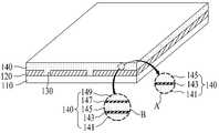
먼저, 도 1a에 도시된 바와 같이, 기판(10)의 전면에 제 1 전극(20)을 형성한 후, 레이저 스크라이빙 공정을 통해 기판(10)의 소정 영역이 노출되도록 제 1 전극(20)을 소정 간격으로 제거하여 전극 분리부(30)를 형성한다.First, as shown in FIG. 1A, after forming the
다음, 도 1b에 도시된 바와 같이, 제 1 전극(20)이 형성된 기판(10)의 전면에 광전 변환층(40)을 형성한다.Next, as shown in FIG. 1B, the
다음, 도 1c에 도시된 바와 같이, 광전 변환층(40) 상에 투명전도층(50)을 형성한다.Next, as illustrated in FIG. 1C, the transparent
다음, 도 1d에 도시된 바와 같이, 레이저 스크라이빙 공정을 통해 제 1 전극(20)의 소정 영역이 노출되도록 광전 변환층(40) 및 투명전도층(50)을 동시에 제거하여 콘택 라인(60)을 형성한다.Next, as shown in FIG. 1D, the
다음, 도 1e에 도시된 바와 같이, 콘택 라인(60)과 투명전도층(50) 상에 제 2 전극(70)을 형성한다. 이때, 제 2 전극(70)은 콘택 라인(60)을 통해 제 1 전극(20)에 전기적으로 접속된다.Next, as shown in FIG. 1E, the
다음, 도 1f에 도시된 바와 같이, 레이저 스크라이빙 공정을 통해 콘택 라인(60)에 인접한 제 1 전극(20)의 소정 영역이 노출되도록 제 2 전극(70), 광전 변환층(40) 및 투명전도층(50)을 동시에 제거하여 셀 분리부(80)를 형성한다.Next, as shown in FIG. 1F, the
이와 같은 일반적인 박막형 태양전지의 제조방법에서는 다음과 같은 문제점이 있다.In the manufacturing method of such a general thin film solar cell has the following problems.
첫째, 레이저 조사장치를 이용한 레이저 스크라이빙 공정을 통해 제 2 전극(70)과 투명 도전층(50) 및 광전 변환층(40)을 동시에 제거하여 셀 분리부(80)를 형성하게 되는데, 기판(10)이 대형화될 수록 레이저 스크라이빙 공정 시간이 오래 걸리며, 레이저 스크라이빙 공정 시간을 단축시키기 위해 복수의 레이저 조사장치를 사용할 경우 비용이 증가한다는 문제점이 있다.First, the
둘째, 건축물의 유리창은 가시권이 보장되어야 하므로, 건축물의 유리창 대용으로 박막형 태양전지를 사용하기 위해서는 어느 정도의 광 투과영역을 확보하여야 한다. 그러나, 광 투과영역은 제 2 전극(70)들 사이의 영역인 셀 분리부(80)에 한정되어 가시권이 보장되지 않기 때문에, 가시권의 보장을 위해 셀 분리부(80)의 폭을 증가시킬 경우 레이저 스크라이빙 공정을 여러 번 수행해야 되므로 생산성이 저하된다는 문제점이 있다.Second, since the visibility of the glass window of the building must be guaranteed, in order to use the thin-film solar cell as a substitute for the glass window of the building, a certain amount of light transmitting area must be secured. However, since the light transmission region is limited to the
본 발명은 상술한 문제점을 해결하기 위한 것으로서, 생산성을 향상시킬 수 있도록 한 박막형 태양전지의 제조 장치 및 제조 방법을 제공하는 것을 기술적 과제로 한다.SUMMARY OF THE INVENTION The present invention has been made in view of the above-described problems, and an object of the present invention is to provide a manufacturing apparatus and a manufacturing method of a thin-film solar cell capable of improving productivity.
또한, 본 발명은 유리창 대용으로 적용하기에 충분한 가시권을 확보할 수 있는 박막형 태양전지의 양산성을 향상시킬 수 있도록 한 박막형 태양전지의 제조 장치 및 제조 방법을 제공하는 것을 기술적 과제로 한다.Another object of the present invention is to provide an apparatus and a method for manufacturing a thin film solar cell, which can improve the mass productivity of a thin film solar cell capable of securing sufficient visibility for application as a glass window.
상술한 기술적 과제를 달성하기 위한 본 발명에 따른 박막형 태양전지의 제조 장치는 기판 전면에 제 1 전극을 형성하는 제 1 전극 형성부; 상기 제 1 전극의 소정 영역을 제거하여 제 1 분리부를 형성하는 전극 분리부; 상기 제 1 전극과 상기 제 1 분리부를 포함하는 기판 전면에 광전 변환층을 형성하는 광전 변환층 형성부; 상기 제 1 전극 상에 형성된 상기 광전 변환층의 소정 영역을 제거하여 콘택 라인을 형성하는 콘택 라인 형성부; 상기 콘택 라인을 통해 상기 제 1 전극에 접속됨과 아울러 제 2 분리부를 사이에 두고 소정 간격으로 이격되는 제 2 전극을 상기 광전 변환층 상에 형성하는 프린팅부; 및 상기 제 2 전극이 형성된 기판을 이송하면서 스프레이 방식의 습식 에칭 공정을 통해 상기 제 2 분리부 내의 상기 광전 변환층을 제거하여 상기 제 2 분리부 내의 상기 제 1 전극을 노출시키는 에칭 공정부를 포함하여 구성되는 것을 특징으로 한다.An apparatus for manufacturing a thin film solar cell according to the present invention for achieving the above technical problem is a first electrode forming unit for forming a first electrode on the front surface of the substrate; An electrode separator to form a first separator by removing a predetermined region of the first electrode; A photoelectric conversion layer forming unit forming a photoelectric conversion layer on an entire surface of the substrate including the first electrode and the first separation unit; A contact line forming unit forming a contact line by removing a predetermined region of the photoelectric conversion layer formed on the first electrode; A printing part connected to the first electrode through the contact line and forming a second electrode on the photoelectric conversion layer spaced at a predetermined interval with a second separation part interposed therebetween; And an etching process unit for exposing the first electrode in the second separation unit by removing the photoelectric conversion layer in the second separation unit through a spray wet etching process while transferring the substrate on which the second electrode is formed. It is characterized in that the configuration.
상기 박막형 태양전지의 제조 장치는 상기 광전 변환층 상에 투명 도전층을 형성하는 투명 도전층 형성부를 더 포함하여 구성되고, 상기 콘택 라인 형성부는 상기 투명 도전층과 상기 광전 변환층의 소정 영역을 함께 제거하여 상기 콘택 라인을 형성하며, 상기 에칭 공정부는 상기 제 2 분리부 내의 상기 투명 도전층과 상기 광전 변환층을 함께 제거하여 상기 제 1 전극을 노출시키는 것을 특징으로 한다.The apparatus for manufacturing a thin film solar cell further includes a transparent conductive layer forming unit for forming a transparent conductive layer on the photoelectric conversion layer, wherein the contact line forming unit combines the transparent conductive layer and a predetermined region of the photoelectric conversion layer together. And forming the contact line, wherein the etching process unit removes the transparent conductive layer and the photoelectric conversion layer in the second separation unit to expose the first electrode.
상기 에칭 공정부는 상기 제 2 전극이 형성된 기판을 이송하는 컨베이어; 상기 컨베이어의 구동에 의해 이송되는 기판을 1차적으로 세정하는 1차 세정부; 상기 컨베이어의 구동에 의해 상기 1차 세정부를 통과하여 이송되는 기판 상에 에칭액을 분사하여 상기 습식 에칭 공정을 수행하는 습식 에칭부; 상기 컨베이어의 구동에 의해 상기 습식 에칭부를 통과하여 이송되는 기판을 2차적으로 세정하는 2차 세정부; 및 상기 컨베이어의 구동에 의해 상기 2차 세정부를 통과하여 이송되는 기판을 건조하는 건조부를 포함하여 구성되는 것을 특징으로 한다.The etching process unit may include a conveyor for transporting the substrate on which the second electrode is formed; A primary cleaning unit which primarily cleans the substrate transported by the conveyor; A wet etching unit for performing the wet etching process by spraying etching liquid onto the substrate transferred through the primary cleaning unit by driving the conveyor; A secondary cleaner for secondary cleaning of the substrate transferred through the wet etching unit by driving of the conveyor; And a drying unit for drying the substrate transported through the secondary cleaning unit by driving of the conveyor.
상기 습식 에칭부는 상기 컨베이어 상에 일정한 간격으로 설치되어 상기 기판 상에 에칭액을 분사하는 복수의 에칭액 분사 노즐; 상기 복수의 에칭액 분사 노즐을 공통적으로 지지하는 노즐 지지부재; 상기 노즐 지지부재를 지지하는 스윙 축; 및 상기 스윙 축을 소정 거리 또는 소정 각도만큼 스윙시키기 위한 구동 수단을 포함하여 구성되는 것을 특징으로 한다.The wet etching unit may include a plurality of etching liquid spray nozzles installed at regular intervals on the conveyor to spray etching liquid onto the substrate; A nozzle support member for supporting the plurality of etching liquid injection nozzles in common; A swing shaft for supporting the nozzle support member; And driving means for swinging the swing axis by a predetermined distance or by a predetermined angle.
상기 에칭 공정부는 상기 1차 세정부와 상기 습식 에칭부 사이에 설치된 제 1 뉴트럴 존(Neutral Zone)을 더 포함하여 구성되며, 제 1 뉴트럴 존은 상기 1차 세정부에 인접하도록 설치되어 상기 1차 세정된 기판이 배출되는 상기 1차 세정부의 기판 배출구 쪽으로 에어(Air)를 분사하는 제 1 에어 커튼; 및 상기 습식 에칭부에 인접하도록 설치되어 상기 제 1 에어 커튼을 통과하는 기판이 투입되는 상기 습식 에칭부의 기판 투입구 쪽으로 에어를 분사하는 제 2 에어 커튼을 포함하여 구성되는 것을 특징으로 한다.The etching process unit may further include a first neutral zone provided between the primary cleaning unit and the wet etching unit, and the first neutral zone is installed to be adjacent to the primary cleaning unit. A first air curtain for injecting air toward the substrate outlet of the primary cleaning unit through which the cleaned substrate is discharged; And a second air curtain installed to be adjacent to the wet etching unit and injecting air toward the substrate inlet of the wet etching unit through which the substrate passing through the first air curtain is introduced.
상기 에칭 공정부는 상기 습식 에칭부와 상기 2차 세정부 사이에 설치된 제 2 뉴트럴 존을 더 포함하여 구성되며, 제 2 뉴트럴 존은 상기 습식 에칭부에 인접하도록 설치되어 상기 습식 공정이 완료된 기판이 배출되는 상기 습식 에칭부의 기판 배출구 쪽으로 에어를 분사하는 제 3 에어 커튼; 및 상기 2차 세정부에 인접하도록 설치되어 상기 제 3 에어 커튼을 통과하는 기판이 투입되는 상기 2차 세정부의 기판 투입구 쪽으로 에어를 분사하는 제 4 에어 커튼을 포함하여 구성되는 것을 특징으로 한다.The etching process unit may further include a second neutral zone provided between the wet etching unit and the secondary cleaning unit, and the second neutral zone is installed to be adjacent to the wet etching unit to discharge the substrate on which the wet process is completed. A third air curtain for injecting air toward the substrate outlet of the wet etching portion; And a fourth air curtain installed to be adjacent to the secondary cleaning unit and injecting air toward the substrate inlet of the secondary cleaning unit through which the substrate passing through the third air curtain is introduced.
상술한 기술적 과제를 달성하기 위한 본 발명에 따른 박막형 태양전지의 제조 방법은 기판 전면에 제 1 전극을 형성하는 공정; 상기 제 1 전극의 소정 영역을 제거하여 제 1 분리부를 형성하는 공정; 상기 제 1 전극과 상기 제 1 분리부를 포함한 기판 전면에 광전 변환층을 형성하는 공정; 상기 제 1 전극 상에 형성된 상기 광전 변환층의 소정 영역을 제거하여 콘택 라인을 형성하는 공정; 상기 콘택 라인을 통해 상기 제 1 전극에 접속됨과 아울러 제 2 분리부를 사이에 두고 소정 간격으로 이격되는 제 2 전극을 상기 광전 변환층 상에 프린팅하는 공정; 및 상기 제 2 전극이 형성된 기판을 이송하면서 스프레이 방식의 습식 에칭 공정을 통해 상기 제 2 분리부 내의 상기 광전 변환층을 제거하여 상기 제 2 분리부 내의 상기 제 1 전극을 노출시키는 공정을 포함하여 이루어지는 것을 특징으로 한다.According to an aspect of the present invention, there is provided a method of manufacturing a thin film solar cell, including: forming a first electrode on a front surface of a substrate; Removing a predetermined region of the first electrode to form a first separator; Forming a photoelectric conversion layer on the entire surface of the substrate including the first electrode and the first separator; Forming a contact line by removing a predetermined region of the photoelectric conversion layer formed on the first electrode; Printing a second electrode on the photoelectric conversion layer, the second electrode being connected to the first electrode through the contact line and spaced at a predetermined interval with a second separation part interposed therebetween; And removing the photoelectric conversion layer in the second separation part to expose the first electrode in the second separation part through a spray wet etching process while transferring the substrate on which the second electrode is formed. It is characterized by.
상기 박막형 태양전지의 제조 방법은 상기 광전 변환층 상에 투명 도전층을 형성하는 공정을 더 포함하여 이루어지며, 상기 콘택 라인 형성시 상기 투명 도전층과 상기 광전 변환층의 소정 영역을 함께 제거하고, 상기 에칭 공정시 상기 제 2 분리부 내의 상기 투명 도전층과 상기 광전 변환층을 함께 제거하는 것을 특징으로 한다.The method of manufacturing the thin film solar cell further includes a step of forming a transparent conductive layer on the photoelectric conversion layer, and removing the predetermined region of the transparent conductive layer and the photoelectric conversion layer together when forming the contact line, In the etching process, the transparent conductive layer and the photoelectric conversion layer in the second separation part may be removed together.
상기 스프레이 방식의 습식 에칭 공정은 컨베이어의 구동에 따라 상기 제 2 전극이 형성된 기판을 연속적으로 이송시키는 단계; 1차 세정부에서 상기 기판을 1차적으로 세정하는 단계; 상기 컨베이어 상에 일정한 간격으로 설치된 복수의 에칭액 분사 노즐을 포함하여 구성된 습식 에칭부에서 상기 복수의 에칭액 분사 노즐을 통해 상기 1차 세정된 기판 상에 에칭액을 분사하여 상기 습식 에칭 공정을 수행하는 단계; 2차 세정부에서 상기 습식 에칭 공정이 완료된 기판을 2차 세정하는 단계; 및 상기 2차 세정된 기판을 건조하는 단계를 포함하여 이루어지는 특징으로 한다.The spray wet etching process may include continuously transferring a substrate on which the second electrode is formed according to driving of a conveyor; First cleaning the substrate in a first cleaning unit; Performing a wet etching process by spraying etching liquid onto the first cleaned substrate through the plurality of etching liquid spray nozzles in a wet etching unit including a plurality of etching liquid spray nozzles installed at regular intervals on the conveyor; Second cleaning the substrate on which the wet etching process is completed in a second cleaning unit; And drying the secondary cleaned substrate.
상기 복수의 에칭액 분사 노즐은 소정 거리 또는 소정 각도만큼 스윙되는 것을 특징으로 한다.The plurality of etching liquid injection nozzles are characterized in that the swing by a predetermined distance or a predetermined angle.
상기 박막형 태양전지의 제조 방법은 상기 1차 세정부에 인접하도록 설치된 제 1 에어 커튼을 이용해 상기 1차 세정된 기판이 배출되는 상기 1차 세정부의 기판 배출구 쪽으로 에어(Air)를 분사하는 단계; 및 상기 습식 에칭부에 인접하게 설치된 제 2 에어 커튼을 이용해 상기 제 1 에어 커튼을 통과하는 기판이 투입되는 상기 습식 에칭부의 기판 투입구 쪽으로 에어를 분사하는 단계를 더 포함하여 이루어지는 것을 특징으로 한다.The manufacturing method of the thin film solar cell may include spraying air toward a substrate outlet of the first cleaning unit through which the first cleaned substrate is discharged using a first air curtain installed adjacent to the first cleaning unit; And injecting air toward a substrate inlet of the wet etching unit, through which the substrate passing through the first air curtain is introduced, using a second air curtain disposed adjacent to the wet etching unit.
상기 박막형 태양전지의 제조 방법은 상기 습식 에칭부에 인접하게 설치된 제 3 에어 커튼을 이용해 상기 습식 공정이 완료된 기판이 배출되는 상기 습식 에칭부의 기판 배출구 쪽으로 에어를 분사하는 단계; 및 상기 2차 세정부에 인접하도록 설치된 제 4 에어 커튼을 이용해 상기 제 3 에어 커튼을 통과하는 기판이 투입되는 상기 2차 세정부의 기판 투입구 쪽으로 에어를 분사하는 단계를 더 포함하여 이루어지는 것을 특징으로 한다.The manufacturing method of the thin-film solar cell may include spraying air toward a substrate outlet of the wet etching unit through which the substrate on which the wet process is completed is discharged by using a third air curtain adjacent to the wet etching unit; And injecting air toward a substrate inlet of the secondary cleaning unit into which the substrate passing through the third air curtain is injected using a fourth air curtain installed adjacent to the secondary cleaning unit. do.
상술한 바와 같이 본 발명에 따른 박막형 태양전지의 제조 장치 및 제조 방법은 프린팅 방식을 이용하여 제 2 전극을 형성한 후, 제 2 전극을 마스크로 한 스프레이 방식의 습식 에칭 공정을 통해 광전 변환부를 분리하는 셀 분리부를 형성하거나, 상기의 셀 분리부와 제 2 전극에 광투과부를 형성함으로써 다음과 같은 효과가 있다.As described above, in the apparatus and method for manufacturing the thin film solar cell according to the present invention, after forming the second electrode using a printing method, the photoelectric conversion unit is separated through a wet etching process using a spray method using the second electrode as a mask. By forming a cell separation unit or forming a light transmitting unit in the cell separation unit and the second electrode, the following effects are obtained.
첫째, 프린팅 공정 및 스프레이 방식의 습식 에칭 공정을 통해 제 2 전극/셀 분리 또는 제 2 전극/셀 분리부/광투과부를 형성함으로써 제 2 전극/셀 분리 또는 제 2 전극/셀 분리부/광투과부의 공정 시간을 단축시켜 생산성을 향상시킬 수 있다.First, the second electrode / cell separation or the second electrode / cell separation unit / light transmission unit by forming the second electrode / cell separation unit or the second electrode / cell separation unit / light transmission unit through a printing process and a wet etching process using a spray method. Productivity can be improved by shortening the process time of the process.
둘째, 종래의 레이저 스크라이빙 공정 대신에 습식 에칭 공정을 통해 셀 분리부와 광투과부를 형성함으로써 유리창 대용으로 적용하기에 충분한 가시권을 확보할 수 있고, 양산성을 향상시킴과 아울러 비용을 감소시킬 수 있다.Second, instead of the conventional laser scribing process, by forming a cell separation part and a light transmitting part through a wet etching process, it is possible to obtain sufficient visibility to be applied as a substitute for a glass window, improve mass productivity and reduce costs. Can be.
도 1a 내지 도 1f는 일반적인 박막형 태양전지의 제조방법을 단계적으로 나타내는 단면도이다.
도 2a 내지 도 2f는 본 발명의 제 1 실시 예에 따른 박막형 태양전지의 제조 방법을 단계적으로 설명하기 위한 단면도이다.
도 3a 내지 도 3f는 본 발명의 제 2 실시 예에 따른 박막형 태양전지의 제조 방법을 단계적으로 설명하기 위한 단면도이다.
도 4a 및 도 4b는 도 3e에 도시된 광 투과 패턴의 다양한 실시 예를 설명하기 위한 도면이다.
도 5는 본 발명의 실시 예에 따른 박막형 태양전지의 제조 장치를 개략적으로 나타내는 블록도이다.
도 6은 도 5에 도시된 에칭 공정부를 개략적으로 나타내는 도면이다.
도 7은 도 6에 도시된 컨베이어를 개략적으로 나타내는 도면이다.
도 8a 내지 도 8c는 도 7에 도시된 습식 에칭부의 실시 예들을 개략적으로 설명하기 위한 도면이다.
도 9는 도 5에 도시된 에칭 공정부의 다른 실시 예를 개략적으로 설명하기 위한 도면이다.
도 10은 도 9에 도시된 제 1 뉴트럴 존을 개략적으로 설명하기 위한 도면이다.1A to 1F are cross-sectional views illustrating a method of manufacturing a general thin film solar cell in steps.
2A to 2F are cross-sectional views for explaining step-by-step a method of manufacturing a thin film solar cell according to a first embodiment of the present invention.
3A to 3F are cross-sectional views for explaining step-by-step a method of manufacturing a thin film solar cell according to a second embodiment of the present invention.
4A and 4B are diagrams for describing various embodiments of the light transmission pattern illustrated in FIG. 3E.
5 is a block diagram schematically illustrating an apparatus for manufacturing a thin film solar cell according to an exemplary embodiment of the present invention.
FIG. 6 is a diagram schematically illustrating an etching process unit illustrated in FIG. 5.
FIG. 7 is a view schematically illustrating the conveyor illustrated in FIG. 6.
8A to 8C are views for schematically describing embodiments of the wet etching unit illustrated in FIG. 7.
FIG. 9 is a view for schematically describing another embodiment of the etching process unit illustrated in FIG. 5.
FIG. 10 is a diagram for schematically describing a first neutral zone illustrated in FIG. 9.
이하 첨부된 도면을 참조하여 본 발명의 실시 예에 대해 상세히 설명한다.Hereinafter, embodiments of the present invention will be described in detail with reference to the accompanying drawings.
도 2a 내지 도 2f는 본 발명의 제 1 실시 예에 따른 박막형 태양전지의 제조 방법을 단계적으로 설명하기 위한 단면도이다.2A to 2F are cross-sectional views for explaining step-by-step a method of manufacturing a thin film solar cell according to a first embodiment of the present invention.
도 2a 내지 도 2f를 참조하여 본 발명의 제 1 실시 예에 따른 박막형 태양전지의 제조 방법을 단계적으로 설명하면 다음과 같다.Referring to FIGS. 2A through 2F, a method of manufacturing a thin film solar cell according to a first embodiment of the present invention will be described below.
먼저, 도 2a에 도시된 바와 같이, 기판(110)의 전면에 제 1 전극(120)을 형성한 후, 레이저 스크라이빙 공정을 통해 기판(110)의 소정 영역이 노출되도록 제 1 전극(120)을 소정 간격으로 제거하여 제 1 분리부(130)를 형성한다.First, as shown in FIG. 2A, after forming the
기판(110)은 유리 기판, 금속 기판, 플라스틱 기판 또는 플렉시블 기판이 될 수 있다. 기판(110)으로 유리 기판을 사용할 경우 태양전지의 생산 단자를 줄일 수 있다. 반면에, 기판(110)으로 금속 기판, 플라스틱 기판 또는 플렉시블 기판을 사용할 경우 태양전지의 박형화 및 경량화를 가능하게 할 수 있고, 플렉시블 태양전지를 제조할 수 있다. 예를 들어, 금속 기판은 알루미늄 또는 스테인리스 재질로 이루어질 수 있고, 플렉시블 기판은 박형(50 ~ 200μm의 두께) 유리, 금속 호일, 플라스틱 재질로 이루어질 수 있다. 플라스틱 재질은 PC(Polycarbonate), PET(Polyethylene terephthalate), PES(Polyethersulfone), PI(Polyimide), PEN(Polyethylene Naphthalate), PEEK(Polyetheretherketone) 등의 열가소성 세미결정성 고분자(Thermoplastic Semicrystalline Polymer) 재질로 이루어질 수 있다.The
제 1 전극(120)은 기판(110) 전면에 SnO2, SnO2:F, SnO2:B, SnO2:Al, 또는 ITO(Indium Tin Oxide) 등의 투명한 도전물질로 형성되는 것이 바람직하다. 이때, 제 1 전극(120)은 CVD(Chemical Vapor Deposition) 공정에 의해 형성될 수 있다.The
한편, 제 1 전극(120)은 태양광이 입사되는 면이기 때문에 입사되는 태양광이 태양전지 내부로 최대한 흡수될 수 있도록 하기 위해서 텍스처(Texturing) 가공 공정을 통해 요철구조를 가지도록 형성될 수 있다. 텍스처 가공 공정이란 물질 표면을 울퉁불퉁한 요철구조로 형성하여 마치 직물의 표면과 같은 형상으로 가공하는 공정으로서, 포토리소그라피법(photolithography)을 이용한 식각공정, 화학용액을 이용한 이방성 식각공정(anisotropic etching), 또는 기계적 스크라이빙(mechanical scribing)을 이용한 홈 형성 공정 등을 통해 수행할 수 있다.On the other hand, since the
다음, 도 2b에 도시된 바와 같이, 제 1 분리부(130)와 제 1 전극(120)이 형성된 기판(100) 전면에 광전 변환층(140)을 형성한다.Next, as shown in FIG. 2B, the
제 1 실시 예에 따른 광전 변환층(140)은 실리콘계 반도체 물질로 형성될 수 있으며, P형 반도체층, I형 반도체층 및 N형 반도체층이 순서대로 적층된 PIN구조로 형성될 수 있다. 여기서, I형 반도체층 대신에 N형 또는 P형 반도체층 보다 얇은 두께의 N형 또는 P형 반도체층이 형성될 수도 있고, I형 반도체층 대신에 N형 또는 P형 반도체층 보다 도핑 농도가 낮은 N형 또는 P형 반도체층이 형성될 수 있다.The
이와 같이 광전 변환층(140)이 PIN구조로 형성되면, I형 반도체층이 P형 반도체층과 N형 반도체층에 의해 공핍(Depletion)이 되어 내부에 전기장이 발생하게 되고, 태양광에 의해 생성되는 정공 및 전자가 상기 전기장에 의해 드리프트(Drift)되어 각각 P형 반도체층 및 N형 반도체층에서 회수되게 된다.When the
그리고, 광전 변환층(140)이 PIN구조로 형성될 경우에는 제 1 전극(120) 상에 P형 반도체층을 형성하고 다음 I형 반도체층 및 N형 반도체층을 형성하는 것이 바람직한데, 그 이유는 일반적으로 정공의 드리프트 이동도(drift mobility)가 전자의 드리프트 이동도에 의해 낮기 때문에 입사광에 의한 회수효율을 극대화하기 위해서 P형 반도체층을 수광면에 가깝게 형성하기 위함이다.When the
한편, 제 2 실시 예에 따른 광전 변환층(140)은 도 2b의 확대도 "A"에 도시된 바와 같이, 제 1 광전 변환층(141), 버퍼층(143), 및 제 2 광전 변환층(145)이 순서대로 적층된 탠덤(Tandem) 구조를 가지도록 형성될 수 있다.On the other hand, the
제 1 광전 변환층(141) 및 제 2 광전 변환층(145) 각각은 P형 반도체 물질층, I형 반도체 물질층 및 N형 반도체 물질층이 순서대로 적층된 PIN 구조를 가지도록 형성된다.Each of the first
버퍼층(143)은 제 1 및 제 2 광전 변환층(141, 145) 사이에서 터널접합을 통해 정공 및 전자의 이동을 원활히 하는 역할을 하는 것으로서, 습식 에칭 공정에 의해 쉽게 제거될 수 있는 투명 도전물질로 형성될 수 있다.The
다른 한편, 제 3 실시 예에 따른 광전 변환층(140)은 도 2b의 확대도 "B"에 도시된 바와 같이, 제 1 광전 변환층(141), 제 1 버퍼층(143), 제 2 광전 변환층(145), 제 2 버퍼층(147), 및 제 2 광전 변환층(149)이 순서대로 적층된 적층된 트리플(Triple) 구조를 가지도록 형성될 수 있다.On the other hand, the
제 1 내지 제 3 광전 변환층(141, 145, 149) 각각은 P형 반도체 물질층, I형 반도체 물질층 및 N형 반도체 물질층이 순서대로 적층된 PIN 구조를 가지도록 형성된다.Each of the first to third photoelectric conversion layers 141, 145, and 149 is formed to have a PIN structure in which a P-type semiconductor material layer, an I-type semiconductor material layer, and an N-type semiconductor material layer are sequentially stacked.
제 1 및 제 2 버퍼층(143, 147) 각각은 제 1 내지 제 3 광전 변환층(141, 145, 149) 사이에서 터널접합을 통해 정공 및 전자의 이동을 원활히 하는 역할을 하는 것으로서, 습식 에칭 공정에 의해 쉽게 제거될 수 있는 투명 도전물질로 형성될 수 있다.Each of the first and second buffer layers 143 and 147 serves to facilitate the movement of holes and electrons through tunnel junctions between the first to third photoelectric conversion layers 141, 145, and 149. It can be formed of a transparent conductive material that can be easily removed by.
다음, 도 2c에 도시된 바와 같이, 광전 변환층(140) 상에 투명 도전층(150)을 형성한다.Next, as illustrated in FIG. 2C, a transparent
투명 도전층(150)은 광전 변환층(140)을 투과한 태양광을 산란시켜 다양한 각으로 진행시킴과 아울러 후술되는 제 2 전극(170)에서 반사되어 광전 변환층(140)으로 재입사되는 광의 비율을 증가시킴으로써 태양전지의 효율을 향상시킨다. 이때, 투명 도전층(150)은 습식 에칭 공정에 의해 쉽게 제거될 수 있는 투명 도전물질, 예를 들어 ZnO, ZnO:B, ZnO:Al, 및 ZnO:H 중 어느 하나의 투명한 도전물질로 형성될 수 있다. 이러한 투명 도전층(150)은 생략될 수 있다.The transparent
다음, 도 2d에 도시된 바와 같이, 레이저 스크라이빙 공정을 통해 제 1 전극(120) 상에 형성된 투명 도전층(150)과 광전 변환층(140)의 소정 영역을 제거하여 콘택 라인(160)을 형성한다. 이때, 콘택 라인(160)은 제 1 분리부(130)에 나란하도록 형성되어 제 1 분리부(130)에 인접한 제 1 전극(120)의 소정 영역을 노출시킨다.Next, as shown in FIG. 2D, the
다음, 도 2e에 도시된 바와 같이, 콘택 라인(160)을 통해 제 1 전극(120)에 접속됨과 아울러 제 2 분리부(180)를 사이에 두고 소정 간격으로 이격되는 제 2 전극(170)을 광전 변환층(140) 상에 프린팅한다. 이때, 제 2 분리부(180)는 콘택 라인(160)에 나란하도록 제 1 전극(120) 상의 투명 도전층(150) 상에 형성되어 제 2 전극(170)을 소정 간격으로 분리한다.Next, as shown in FIG. 2E, the
제 2 전극(170)은 Ag, Al, Cu, Ag+Mo, Ag+Ni, 또는 Ag+Cu 등을 포함하는 금속 페이스트(Paste)를 이용한 한 번의 프린팅 공정에 의해 형성될 수 있다.The
프린팅 공정은 스크린 프린팅(Screen Printing), 잉크젯 프린팅(Inkjet Printing), 그라비아 프린팅(Gravure Printing), 그라비아 오프셋 프린팅(Gravure Offset Printing), 리버스 프린팅(Reverse Printing), 플렉소 프린팅(Flexo Printing), 또는 마이크로 콘택 프린팅(Micro Contact Printing) 방법이 될 수 있다. 여기서, 스크린 프린팅 방법은 스크린 위에 잉크를 올리고, 일정 압력으로 스퀴지(Squeegee)를 가압하면서 이동시켜 스크린의 메쉬를 통해 잉크를 전사하는 방식이다. 잉크젯 프린팅 방법은 매우 작은 잉크 방울을 기판에 충돌시켜 프린팅하는 방식이다. 그라비아 프린팅 방법은 평평한 비화선부에 묻어 있는 잉크를 닥터 블레이드로 제거하고 에칭되어 오목한 화선부에 묻어 있는 잉크만을 기판에 전이시켜 프린팅하는 방식이다. 그라비아 오프셋 프린팅 방법은 잉크를 인쇄판에서 블랑켓에 전사하고 그 블랑켓의 잉크를 다시 기판에 전사하는 방식이다. 리버스 프린팅 방법은 용매를 잉크로 이용하여 프린팅하는 방식이다. 플렉소 프린팅 방법은 양각되어 있는 부분에 잉크를 묻혀서 이를 프린트하는 방식이다. 마이크로 콘택 프린팅 방법은 스탬프에 원하는 물질을 올려 도장처럼 찍어 프린팅하는 방식이다.The printing process can be screen printing, inkjet printing, gravure printing, gravure offset printing, reverse printing, flexo printing, or micro It may be a micro-contact printing method. Here, the screen printing method is a method of transferring the ink through the mesh of the screen by raising the ink on the screen, moving while pressing a squeegee (Squeegee) at a predetermined pressure. An inkjet printing method is a method in which very small ink droplets collide with a substrate for printing. The gravure printing method is a method of removing ink on a flat non-wire portion with a doctor blade and transferring only ink on an etched concave wire portion to a substrate by printing. The gravure offset printing method is a method of transferring ink from a printing plate to a blanket and transferring the ink of the blanket back to a substrate. Reverse printing method is a method of printing using a solvent as an ink. Flexo printing is a method of printing ink by embossing the embossed portion. The micro contact printing method is a method of printing a desired material on a stamp by stamping it like a stamp.
한편, 상술한 프린팅 공정을 통해 제 2 전극(170)을 프린팅한 후, 프린팅된 제 2 전극(170)을 소성하는 소성 공정을 추가로 수행할 수 있다.Meanwhile, after printing the
다음, 도 2f에 도시된 바와 같이, 제 2 전극(170)을 마스크로 한 습식 에칭 공정을 통해 제 2 분리부(180) 내의 투명 도전층(150)과 광전 변환층(140)을 일괄적으로 제거하여 제 1 전극(120)을 노출시킴으로써 광전 변환부(140)를 분리하는 셀 분리부(182)를 형성한다.Next, as illustrated in FIG. 2F, the transparent
습식 에칭 공정에서는 컨베이어를 이용하여 기판(110)을 연속적으로 이송하면서 1차 세정 공정, 에칭 공정, 2차 세정 공정, 및 건조 공정이 연속적으로 수행한다.In the wet etching process, the first cleaning process, the etching process, the second cleaning process, and the drying process are continuously performed while continuously transporting the
1차 세정 공정은 이물질 제거 공정 및 제 1 린스 공정을 포함하여 수행될 수 있다.The primary cleaning process may be performed including a foreign material removal process and a first rinse process.
이물질 제거 공정은 고압의 제 1 초순수(DI)를 기판(110) 상에 분사하여 기판(110) 상의 이물질을 제거한다. 이때, 고압의 제 1 초순수는 기판(110)의 상부 및 하부에 분사될 수 있다.In the foreign material removal process, the high-pressure first ultrapure water DI is sprayed on the
제 1 린스 공정은 제 2 초순수를 이물질 제거 공정이 완료된 기판(110) 상에 분사하여 기판(110)을 린스(Rinse)(또는 세정)한다. 이때, 제 2 초순수는 기판(110)의 상부 및 하부에 분사될 수 있다. 한편, 제 1 린스 공정에서 사용된 후 회수되는 제 2 초순수는 이물질 제거 공정시 사용되는 제 1 초순수로 사용될 수 있다.In the first rinse process, the second ultrapure water is sprayed onto the
에칭 공정은 알칼리성 용액을 통해 제 2 분리부(180) 내의 투명 도전층(150)과 광전 변환층(140)을 일괄적으로 제거하여 제 1 전극(120)을 노출시킨다.The etching process collectively removes the transparent
에칭 공정은 스프레이(Spray) 방식을 이용해 알칼리성 에칭액을 기판(110) 상에 분사하여 제 2 분리부(180) 내의 투명 도전층(150)과 광전 변환층(140)을 일괄적으로 제거한다. 이때, 알칼리성 에칭액은 0.5Pa ~ 2Pa의 압력으로 분사될 수 있으며, 분사되는 알칼리성 에칭액은 기판(110)의 전면에 대하여 서로 중첩되도록 분사되는 것이 바람직하다.In the etching process, an alkaline etching solution is sprayed onto the
알칼리성 에칭액은 NaOH 또는 KOH와 같은 알칼리계에서 선택된 적어도 하나의 용액으로 사용할 수 있고, HCl, HNO3, H2SO4, H3PO3, H2O2, 또는 C2H2O4와 같은 산성 용액에서 선택된 적어도 하나의 용액을 사용할 수 있다. 이때, OH 계열의 알칼리계 에칭 용액을 사용하는 것이 최적이지만, H 계열의 산성계 에칭 용액도 사용할 수 있다.The alkaline etching solution may be used as at least one solution selected from an alkali system such as NaOH or KOH, and may be HCl, HNO3 , H2 SO4 , H3 PO3 , H2 O2 , or C2 H2 O4. At least one solution selected from acidic solutions can be used. At this time, it is optimal to use an OH-based alkali etching solution, but an H-based acid etching solution may also be used.
알칼리성 에칭액은 물로 희석하여 이용할 수 있는데, 이 경우 알칼리성 용액의 농도는 5% ~ 20% 범위인 것이 바람직하다. 그리고, 알칼리성 에칭액의 온도는 60℃ ~ 80℃로 유지하는 것이 바람직하며, 에칭 시간은 40초 ~ 80초 범위인 것이 바람직하다.The alkaline etching solution may be diluted with water, and in this case, the concentration of the alkaline solution is preferably in the range of 5% to 20%. And it is preferable to maintain the temperature of alkaline etching liquid at 60 degreeC-80 degreeC, and it is preferable that an etching time is 40 second-80 second.
한편, 에칭 공정에서 제 2 분리부(180) 내에 형성된 제 1 전극(120)은 알칼리성 에칭액에 쉽게 제거되지 않는 SnO2, SnO2:F, SnO2:B, SnO2:Al, 또는 ITO(Indium Tin Oxide) 등의 투명한 도전물질로 형성되었기 때문에 상기의 에칭 공정에 의해 제 1 전극(120)이 손상되지 않는다.Meanwhile, in the etching process, the
2차 세정 공정은 제 2 린스 공정 및 파이널(Final) 린스 공정을 포함하여 수행될 수 있다.The secondary cleaning process may be performed including a second rinse process and a final rinse process.
제 2 린스 공정은 제 3 초순수를 에칭 공정이 완료된 기판(110) 상에 분사하여 기판(110) 상의 잔류하는 알칼리성 에칭액을 린스(또는 세정)한다. 이때, 제 3 초순수는 기판(110)의 상부 및 하부에 분사될 수 있다. 한편, 제 2 린스 공정에서 사용된 후 회수되는 제 3 초순수는 제 1 린스 공정시 사용되는 제 2 초순수로 사용될 수 있다.In the second rinse process, the third ultrapure water is sprayed onto the
파이널 린스 공정은 제 4 초순수를 제 2 린스 공정이 완료된 기판(110) 상에 분사하여 기판(110)을 최종적으로 린스한다. 이때, 제 4 초순수는 기판(110)의 상부 및 하부에 분사될 수 있다. 한편, 파이널 린스 공정에서 사용된 후 회수되는 제 4 초순수는 제 2 린스 공정시 사용되는 제 3 초순수로 사용될 수 있다.The final rinse process sprays the fourth ultrapure water onto the
건조 공정은 에어 나이프(Air Knife)를 이용하여 파이널 린스 공정을 마친 기판(110)을 건조한다. 이때, 에어 나이프는 기판(110)의 이송 방향에 대하여 소정 각도로 경사지도록 설치되는 것이 바람직하다.The drying process is to dry the
이와 같은, 본 발명의 제 1 실시 예에 따른 박막형 태양전지의 제조 방법은 프린팅 방식을 이용하여 제 2 전극(170)을 형성한 후, 스프레이 방식의 습식 에칭 공정을 통해 광전 변환부(140)를 분리하는 셀 분리부(182)를 형성함으로써 셀 분리부(182)를 형성하기 위한 공정 시간을 줄일 수 있으며, 레이저 스크라이빙 공정을 사용하지 않기 때문에 비용을 감소시킬 수 있다. 여기서, 제 2 전극(170)은 금속 재질로 형성되기 때문에 상술한 습식 에칭을 하여도 식각이 되지 않는 성질을 가지는 마스크 역할을 할 수 있어서, 스프레이 방식의 습식 에칭 공정시 제 2 전극(170)을 마스크로 하여 제 2 분리부 내의 영역만을 식각할 수 있다.As described above, in the method of manufacturing the thin film solar cell according to the first embodiment of the present invention, after forming the
도 3a 내지 도 3f는 본 발명의 제 2 실시 예에 따른 박막형 태양전지의 제조 방법을 단계적으로 설명하기 위한 단면도이다.3A to 3F are cross-sectional views for explaining step-by-step a method of manufacturing a thin film solar cell according to a second embodiment of the present invention.
도 3a 내지 도 3f를 참조하여 본 발명의 제 2 실시 예에 따른 박막형 태양전지의 제조 방법을 단계적으로 설명하면 다음과 같다.Referring to FIGS. 3A to 3F, a method of manufacturing a thin film solar cell according to a second exemplary embodiment of the present invention will be described below.
우선, 본 발명의 제 2 실시 예에 따른 박막형 태양전지의 제조 방법은 건축물의 유리창 대용으로 사용되는 박막형 태양전지의 제조 방법에 관한 것이다. 상술한 실시 예와 동일한 구성에 대한 구체적인 설명은 생략하기로 하고, 동일한 도면 부호를 부여하기로 한다.First, a method of manufacturing a thin film solar cell according to a second embodiment of the present invention relates to a method of manufacturing a thin film solar cell used as a substitute for a glass window of a building. Detailed description of the same configuration as the above-described embodiment will be omitted, and the same reference numerals will be given.
먼저, 도 3a에 도시된 바와 같이, 기판(110)의 전면에 제 1 전극(120)을 형성한 후, 레이저 스크라이빙 공정을 통해 기판(110)의 소정 영역이 노출되도록 제 1 전극(120)을 소정 간격으로 제거하여 제 1 분리부(130)를 형성한다.First, as shown in FIG. 3A, after forming the
다음, 도 3b에 도시된 바와 같이, 제 1 분리부(130)와 제 1 전극(120)이 형성된 기판(100) 전면에 광전 변환층(140)을 형성한다.Next, as shown in FIG. 3B, the
다음, 도 3c에 도시된 바와 같이, 광전 변환층(140) 상에 투명 도전층(150)을 형성한다.Next, as illustrated in FIG. 3C, a transparent
다음, 도 3d에 도시된 바와 같이, 레이저 스크라이빙 공정을 통해 제 1 전극(120) 상에 형성된 투명 도전층(150)과 광전 변환층(140)의 소정 영역을 제거하여 콘택 라인(160)을 형성한다. 이때, 콘택 라인(160)은 제 1 분리부(130)에 나란하도록 형성되어 제 1 분리부(130)에 인접한 제 1 전극(120)의 소정 영역을 노출시킨다.Next, as shown in FIG. 3D, the
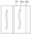
다음, 도 3e에 도시된 바와 같이, 콘택 라인(160)을 통해 제 1 전극(120)에 접속됨과 아울러 제 2 분리부(180)를 사이에 두고 소정 간격으로 이격되는 제 2 전극(170)을 광전 변환층(140) 상에 프린팅한다. 이때, 제 2 분리부(180)는 콘택 라인(160)에 나란하도록 제 1 전극(120) 상의 투명 도전층(150) 상에 형성되어 제 2 전극(170)을 소정 간격으로 분리하기 위한 셀 분리 패턴(182a), 및 제 2 전극(170)이 소정 패턴으로 제거되어 형성된 광투과 패턴(184a)을 포함하여 구성된다.Next, as illustrated in FIG. 3E, the
한편, 상술한 프린팅 공정을 통해 제 2 전극(170)을 프린팅한 후, 프린팅된 제 2 전극(170)을 소성하는 소성 공정을 추가로 수행할 수 있다.Meanwhile, after printing the
다음, 도 3f에 도시된 바와 같이, 제 2 전극(170)을 마스크로 한 습식 에칭 공정을 통해 셀 분리 패턴(182a)과 광투과 패턴(184a) 내의 투명 도전층(150)과 광전 변환층(140)을 일괄적으로 제거하여 제 1 전극(120)을 노출시킴으로써 광전 변환부(140)를 분리하는 셀 분리부(182)를 형성함과 동시에 태양광이 투과하도록 제 1 전극(120)을 노출시키는 광투과부(184)를 형성한다. 여기서, 습식 에칭 공정은 알칼리성 에칭액을 이용한 스프레이(Spray) 방식을 사용하는 것으로 상술한 제 1 실시 예의 제조 방법과 동일하므로 이에 대한 설명은 상술한 설명으로 대신하기로 한다.Next, as shown in FIG. 3F, the transparent
한편, 상술한 제 2 분리부(180)의 광투과 패턴(184a)은 도 3f에 도시된 바와 같이, 셀 분리 패턴(182a)에 교차하는 스트라이프(Stripe) 형태로 형성될 수 있지만, 이에 한정되지 않고, 다양한 형태로 형성될 수 있다. 예를 들어, 광투과 패턴(184a)은 도 4a에 도시된 바와 같이 곡선 형태로 형성되거나, 도 4b에 도시된 바와 같이 문자 형태로 마련될 수도 있다. 또한, 도시하지 않았지만, 광투과 패턴(184a)은 도형, 기호, 및 숫자 형태 중 적어도 하나의 형태로 형성될 수도 있으며, 필요에 따라 다양한 형태로 형성될 수 있다.Meanwhile, the
이와 같은, 본 발명의 제 2 실시 예에 따른 박막형 태양전지의 제조 방법은 프린팅 방식을 이용하여 제 2 전극(170)을 형성한 후, 제 2 전극(170)을 마스크로 한 스프레이 방식의 습식 에칭 공정을 통해 광전 변환부(140)를 분리하는 셀 분리부(182)를 형성함 동시에 제 2 전극(170)에 광투과부(184)를 형성함으로써 레이저 스크라이빙 공정을 사용하지 않기 때문에 비용을 감소시킴과 아울러, 종래의 레이저 스크라이빙 공정 대비 공정시간이 오래 걸리지도 않으면서 셀 분리부(182)와 광투과부(184)를 통해 유리창 대용으로 적용하기에 충분한 가시권을 확보할 수 있고, 대량 생산에 유리하다.As described above, in the method of manufacturing the thin film solar cell according to the second embodiment of the present invention, after forming the
도 5는 본 발명의 실시 예에 따른 박막형 태양전지의 제조 장치를 개략적으로 나타내는 블록도이다.5 is a block diagram schematically illustrating an apparatus for manufacturing a thin film solar cell according to an exemplary embodiment of the present invention.
도 5를 참조하면, 본 발명의 실시 예에 따른 박막형 태양전지의 제조 장치는 로더부(200), 제 1 전극 형성부(210), 전극 분리부(220), 광전 변환층 형성부(230), 콘택 라인 형성부(240), 프린팅부(250), 소성부(260), 에칭 공정부(270), 및 언로더부(280)를 포함하여 구성된다.Referring to FIG. 5, the apparatus for manufacturing a thin film solar cell according to an exemplary embodiment of the present invention may include a
로더부(200)는 기판(미도시)을 제 1 전극 형성부(210)에 공급한다. 이때, 기판은 유리 기판, 금속 기판, 플라스틱 기판 또는 플렉시블 기판이 될 수 있다.The
제 1 전극 형성부(210)는, 도 2a 또는 도 3a에 도시된 바와 같이, 로더부(200)에 의해 공급되는 기판의 전면에 SnO2, SnO2:F, SnO2:B, SnO2:Al, 또는 ITO(Indium Tin Oxide) 등의 투명한 도전물질 이루어지는 제 1 전극(120)을 형성한다. 이때, 제 1 전극 형성부(210)는 CVD(Chemical Vapor Deposition) 공정을 통해 상기의 제 1 전극(120)을 형성할 수 있다. 이러한, 제 1 전극 형성부(210)는 클러스터(Cluster) 형태로 구성되거나 인라인 형태로 구성된다.As shown in FIG. 2A or FIG. 3A, the first
전극 분리부(220)는, 도 2a 또는 도 3a에 도시된 바와 같이, 제 1 전극 형성부(210)에 의해 기판의 전면에 형성된 제 1 전극(120)의 소정 영역을 제거하여 제 1 전극(120)을 소정 간격으로 분리하는 제 1 분리부(130)를 형성한다. 이때, 전극 분리부(220)는 레이저 스크라이빙 공정을 이용하여 제 1 분리부(130)를 형성할 수 있다.As shown in FIG. 2A or FIG. 3A, the
한편, 제 1 전극(120)은 태양광이 입사되는 면이기 때문에 입사되는 태양광이 태양전지 내부로 최대한 흡수될 수 있도록 하는 것이 중요하며, 이를 위해, 제 1 전극 형성부(210)과 전극 분리부(220) 사이에는 제 1 전극(120)의 표면에 텍스처(Texturing)를 형성하기 위한 텍스처링부(미도시)가 설치되는 것이 바람직하다.On the other hand, since the
광전 변환층 형성부(230)는, 도 2b 또는 도 3b에 도시된 바와 같이, 제 1 전극(120)과 제 1 분리부(130)가 형성된 기판의 전면에 광전 변환층(140)을 형성한다. 이러한, 광전 변환층 형성부(230)는 클러스터 형태로 배치되어 화학기상증착 공정을 수행하는 복수의 공정 챔버를 이용하여 기판의 전면에 P형 반도체 물질, I형 반도체 물질 및 N형 반도체 물질이 순서대로 적층된 PIN구조로 적어도 하나의 광전 변환층(140)을 형성한다. 이때, 도 2b 또는 도 3b에 도시된 확대도 "A" 또는 "B"와 같이 광전 변환층(140)이 복수로 적층된 구조, 즉 탠덤 또는 트리플 구조를 가지도록 형성되는 경우 광전 변환층들(141, 145, 149) 사이에는 버퍼층(143, 147)이 형성된다.As shown in FIG. 2B or 3B, the photoelectric conversion
한편, 본 발명의 실시 예에 따른 박막형 태양전지의 제조 장치는, 도 2c 또는 도 3c에 도시된 바와 같이, 광전 변환층(140) 상에 투명 도전층(150)을 형성하기 위한 투명 도전층 형성부(235)를 더 포함하여 구성될 수 있다.Meanwhile, in the apparatus for manufacturing a thin film solar cell according to an exemplary embodiment of the present invention, as illustrated in FIG. 2C or 3C, a transparent conductive layer for forming the transparent
투명 도전층 형성부(235)는 MOCVD 공정 또는 PECVD 공정을 이용하여 광전 변환층(140) 상에 투명 도전층(150)을 형성한다. 이때, 투명 도전층(150)은 습식 에칭 공정에 의해 쉽게 제거될 수 있는 투명 도전물질, 예를 들어 ZnO, ZnO:B, ZnO:Al, 및 ZnO:H 중 어느 하나의 투명한 도전물질로 형성될 수 있다. 이러한 투명 도전층(150)은 태양전지의 구조에 따라 생략될 수 있으며, 이 경우 투명 도전층 형성부(245) 역시 생략된다.The transparent conductive
콘택 라인 형성부(240)는, 도 2d 또는 도 3d에 도시된 바와 같이, 제 1 분리부(130)에 인접한 제 1 전극(120) 상에 형성된 투명 도전층(150)과 광전 변환층(140)의 소정 영역을 제거하여 콘택 라인(160)을 형성한다. 이에 따라, 광전 변환층(140)은 콘택 라인(160)을 사이에 두고 소정 간격으로 이격된다. 이러한, 콘택 라인 형성부(240)는 레이저 스크라이빙 공정을 이용하여 콘택 라인(160)을 형성할 수 있다.As illustrated in FIG. 2D or 3D, the contact
제 1 실시 예에 따른 프린팅부(250)는, 도 2e에 도시된 바와 같이, 콘택 라인(160)을 통해 제 1 전극(120)에 접속됨과 아울러 제 2 분리부(180)를 사이에 두고 소정 간격으로 이격되는 제 2 전극(170)을 투명 도전층(150) 상에 프린팅한다. 이때, 제 2 분리부(180)는 콘택 라인(160)에 나란하도록 제 1 전극(120) 상의 투명 도전층(150) 상에 형성되어 제 2 전극(170)을 소정 간격으로 분리한다.As illustrated in FIG. 2E, the
프린팅부(250)는 Ag, Al, Cu, Ag+Mo, Ag+Ni, 또는 Ag+Cu 등을 포함하는 금속 페이스트(Paste)를 이용한 한 번의 프린팅 공정에 의해 제 2 전극(170)을 형성한다.The
한편, 프린팅부(250)는 상술한 스크린 프린팅(Screen Printing), 잉크젯 프린팅(Inkjet Printing), 그라비아 프린팅(Gravure Printing), 그라비아 오프셋 프린팅(Gravure Offset Printing), 리버스 프린팅(Reverse Printing), 플렉소 프린팅(Flexo Printing), 또는 마이크로 콘택 프린팅(Micro Contact Printing) 방법을 이용하여 프린팅 공정을 수행할 수 있다.The
제 2 실시 예에 따른 프린팅부(250)는, 도 3e에 도시된 바와 같이, 콘택 라인(160)을 통해 제 1 전극(120)에 접속됨과 아울러 제 2 분리부(180)를 사이에 두고 소정 간격으로 이격되는 제 2 전극(170)을 투명 도전층(150) 상에 프린팅한다. 이때, 제 2 분리부(180)는 콘택 라인(160)에 나란하도록 제 1 전극(120) 상의 투명 도전층(150) 상에 형성되어 제 2 전극(170)을 소정 간격으로 분리하기 위한 셀 분리 패턴(182a), 및 셀 분리 패턴(182a)에 의해 분리된 제 2 전극(170)이 소정 패턴으로 제거된 광투과 패턴(184a)을 포함한다.As illustrated in FIG. 3E, the
프린팅부(250)는 Ag, Al, Cu, Ag+Mo, Ag+Ni, 또는 Ag+Cu 등을 포함하는 금속 페이스트(Paste)를 이용하여 상술한 한 번의 프린팅 공정에 의해 제 2 전극(170)을 형성한다.The
소성부(260)는 프린팅부(250)에 의해 제 2 전극(170)이 프린팅된 기판을 가열 등의 열처리를 통해 제 2 전극(170)의 페이스트에서 휘발되는 솔벤트를 제거하여 제 2 전극(170)을 소성한다.The
에칭 공정부(270)는 제 2 전극(170)을 마스크로 한 스프레이(Spray) 방식의 습식 에칭 공정을 수행함으로써, 도 2f에 도시된 바와 같이, 제 2 분리부(180) 내의 투명 도전층(150)과 광전 변환층(140)을 함께 제거하여 제 1 전극(120)을 노출시키는 셀 분리부(182)를 형성하거나, 도 3f에 도시된 바와 같이, 제 2 분리부(180)의 셀 분리 패턴(182a)과 광투과 패턴(184a) 내의 투명 도전층(150)과 광전 변환층(140)을 함께 제거하여 제 1 전극(120)을 노출시키는 셀 분리부(182)와 광투과부(184)를 형성한다.The
언로더부(280)는 에칭 공정부(270)에 의해 에칭 공정이 완료된 기판을 외부로 언로딩한다.The
도 6은 도 5에 도시된 에칭 공정부를 개략적으로 나타내는 도면이다.FIG. 6 is a diagram schematically illustrating an etching process unit illustrated in FIG. 5.
도 6을 도 5와 결부하면, 에칭 공정부(270)는 컨베이어(310), 베스(320), 1차 세정부(330, 340), 습식 에칭부(350), 2차 세정부(360, 370), 및 건조부(380)를 포함하여 구성된다.6, the
컨베이어(310)는 베스(320)의 측면을 관통하도록 설치되어 제 2 전극(170)이 형성된 기판(110)을 이송한다. 이를 위해, 컨베이어(310)는, 도 7에 도시된 바와 같이, 제 1 및 제 2 컨베이어 프레임(311a, 311b), 복수의 구동축(313), 복수의 롤러(315), 구동 모터(317), 및 복수의 가이드 롤러(319)를 포함하여 구성된다.The
제 1 및 제 2 컨베이어 프레임(311a, 311b)는 소정 간격으로 이격되도록 나란하게 설치된다.The first and
복수의 구동축(313) 각각은 제 1 및 제 2 컨베이어 프레임(311a, 311b) 간에 소정 간격을 가지도록 회전 가능하게 설치된다.Each of the plurality of
복수의 롤러(315)는 복수의 구동축(313) 각각에 소정 간격으로 설치되어 구동축(313)의 회전에 따라 기판(110)을 이송한다.The plurality of
구동 모터(317)는 제 1 컨베이어 프레임(311a)의 외측면에는 설치되어 복수의 구동축(313)을 동시에 회전시킨다. 이때, 구동 모터(317)의 회전력은 제 1 컨베이어 프레임(311a)의 내부에 설치된 회전 전달 부재(미도시)를 통해 복수의 구동축(313) 각각에 전달된다. 회전 전달 부재는 구동 모터(317)의 회전축과 복수의 구동축(313) 각각에 접속되는 것으로, 체인 모듈, 기어 모듈, 또는 벨트 모듈로 구성될 수 있다.The
복수의 가이드 롤러(319) 각각은 제 1 및 제 2 컨베이어 프레임(311a, 311b) 각각의 상면에 소정 간격으로 회전 가능하게 설치되어 복수의 롤러(315)에 의해 이송되는 기판(110)의 양측면을 가이드함으로써 컨베이어(310)에서 기판(110)이 이탈되는 것을 방지한다.Each of the plurality of
베스(320)는 컨베이어(310)를 덮도록 설치되어 습식 에칭 공정을 위한 공간을 제공한다. 이때, 컨베이어(310)는 챔버(320)의 일측벽 및 타측벽을 관통하도록 설치되어 기판(110)을 수평 방향으로 이송한다.The
한편, 베스(320)는 컨베이어(310)에 의해 이송되는 기판(110)에 대한 습식 에칭 공정을 수행하기 위한 복수의 공간으로 분할된다. 즉, 베스(320)는 이물질 제거부(330) 및 제 1 린스부(340)가 설치되는 제 1 린스 존(Rinse Zone)(322), 습식 에칭부(350)가 설치되는 에칭 존(etching Zone)(324), 제 2 린스부(360)와 파이널 린스부(370)가 설치되는 제 2 린스 존(326), 및 건조부(380)가 설치되는 드라이 존(Dry Zone)(328)으로 분할된다.Meanwhile, the
1차 세정부(330, 340)는 이물질 제거부(330) 및 제 1 린스부(340)를 포함하여 구성될 수 있다.The
이물질 제거부(330)는 제 1 린스 존(322)의 일측에 설치되어 컨베이어(310)의 구동에 의해 이송되는 기판(110) 상에 고압의 제 1 초순수를 분사하여 기판(110) 상의 이물질을 제거한다. 이를 위해, 이물질 제거부(330)는 적어도 2개의 제 1 분사 노즐(332)을 포함하여 구성된다.The foreign
적어도 2개의 제 1 분사 노즐(332)은 컨베이어(310) 상부에 위치하도록 제 1 린스 존(322)의 일측 상부에 일정한 간격으로 설치되어 고압의 제 1 초순수를 기판(110) 상에 분사하여 기판(110) 상의 이물질을 제거한다. 여기서, 적어도 2개의 제 1 분사 노즐(332)은 컨베이어(310)를 사이에 두고 제 1 린스 존(322)의 일측 상부 및 하부에 일정한 간격으로 설치되어 기판(110)의 상부면과 하부면에 제 1 초순수를 분사할 수도 있다.At least two
제 1 린스부(340)는 이물질 제거부(330)에 인접하도록 제 1 린스 존(322)의 타측에 설치되어 컨베이어(310)의 구동에 의해 이송되는 기판(110) 상에 제 2 초순수를 분사하여 기판(110)을 린스(또는 세정)한다. 이를 위해, 제 1 린스부(340)는 적어도 2개의 제 2 분사 노즐(342)을 포함하여 구성된다.The first rinse
적어도 2개의 제 2 분사 노즐(342)은 컨베이어(310) 상부에 위치하도록 제 1 린스 존(322)의 타측 상부에 일정한 간격으로 설치되어 이물질 제거부(330)를 통과하여 이송되는 기판(110) 상에 제 2 초순수를 분사하여 기판(110)을 린스한다. 이때, 적어도 2개의 제 2 분사 노즐(342) 각각에서 분사되는 제 2 초순수는 기판(110)에 대하여 서로 중첩되도록 분사되는 것이 바람직하다.At least two
적어도 2개의 제 2 분사 노즐(342)은 컨베이어(310)를 사이에 두고 제 1 린스 존(322)의 타측 상부 및 하부에 일정한 간격으로 설치되어 기판(110)의 상부면과 하부면에 제 2 초순수를 분사할 수도 있다.At least two
한편, 제 1 린스부(340)에서 사용된 후 회수되는 제 2 초순수는 이물질 제거부(330)에서 사용되는 제 1 초순수로 사용될 수 있다.Meanwhile, the second ultrapure water recovered after being used in the first rinse
습식 에칭부(350)는 컨베이어(310)의 구동에 의해 제 1 린스부(340)를 통과하여 이송되는 기판(110) 상에 알칼리성 에칭액을 분사하여 기판(110) 상에 형성된 제 2 전극(170)을 마스크로 한 에칭 공정을 수행함으로써, 도 2f에 도시된 바와 같이, 제 2 분리부(180) 내의 투명 도전층(150)과 광전 변환층(140)을 함께 제거하여 제 1 전극(120)을 노출시키는 셀 분리부(182)를 형성하거나, 도 3f에 도시된 바와 같이, 제 2 분리부(180)의 셀 분리 패턴(182a)과 광투과 패턴(184a) 내의 투명 도전층(150)과 광전 변환층(140)을 함께 제거하여 제 1 전극(120)을 노출시키는 셀 분리부(182)와 광투과부(184)를 형성한다.The
이를 위해, 제 1 실시 예에 따른 습식 에칭부(350)는 복수의 에칭액 분사 노즐(352)을 포함하여 구성된다.To this end, the
복수의 에칭액 분사 노즐(352) 각각은 컨베이어(310) 상에 위치하도록 에칭 존(324)의 상부에 일정한 간격으로 설치되어 기판(110) 상에 알칼리성 에칭액을 분사한다. 이때, 복수의 에칭액 분사 노즐(352) 각각에서 분사되는 알칼리성 에칭액은 0.5Pa ~ 2Pa의 압력으로 분사될 수 있으며, 분사되는 알칼리성 에칭액은 기판(110)의 전면에 대하여 서로 중첩되도록 분사되는 것이 바람직하다.Each of the plurality of etching
알칼리성 에칭액은 NaOH 또는 KOH와 같은 알칼리계에서 선택된 적어도 하나의 용액으로 사용할 수 있고, HCl, HNO3, H2SO4, H3PO3, H2O2, 또는 C2H2O4와 같은 산성 용액에서 선택된 적어도 하나의 용액을 사용할 수 있다. 이때, OH 계열의 알칼리계 에칭 용액을 사용하는 것이 최적이지만, H 계열의 산성계 에칭 용액도 사용할 수 있다.The alkaline etching solution may be used as at least one solution selected from an alkali system such as NaOH or KOH, and may be HCl, HNO3 , H2 SO4 , H3 PO3 , H2 O2 , or C2 H2 O4. At least one solution selected from acidic solutions can be used. At this time, it is optimal to use an OH-based alkali etching solution, but an H-based acid etching solution may also be used.
그리고, 알칼리성 에칭액은 물로 희석하여 이용할 수 있는데, 이 경우 알칼리성 용액의 농도는 5% ~ 20% 범위인 것이 바람직하다. 그리고, 알칼리성 에칭액의 온도는 60℃ ~ 80℃로 유지하는 것이 바람직하며, 에칭 시간은 40초 ~ 80초 범위인 것이 바람직하다.In addition, the alkaline etching solution may be diluted with water, and in this case, the concentration of the alkaline solution is preferably in the range of 5% to 20%. And it is preferable to maintain the temperature of alkaline etching liquid at 60 degreeC-80 degreeC, and it is preferable that an etching time is 40 second-80 second.
한편, 에칭 공정에서 제 2 분리부(180) 내에 형성된 제 1 전극(120)은 알칼리성 에칭액에 쉽게 제거되지 않는 도전물질로 형성되었기 때문에 상기의 에칭 공정에 의해 제 1 전극(120)이 손상되지 않는다.In the etching process, since the
제 2 실시 예에 따른 습식 에칭부(350)는, 도 8a에 도시된 바와 같이, 복수의 에칭액 분사 노즐(352), 노즐 지지부재(354), 스윙 축(356), 및 구동 수단(358)을 포함하여 구성된다.As shown in FIG. 8A, the
복수의 에칭액 분사 노즐(352) 각각은 컨베이어(310) 상에 위치하도록 에칭 존(324)의 상부에 일정한 간격으로 설치되어 기판(110) 상에 상술한 알칼리성 에칭액을 분사한다.Each of the plurality of etching
노즐 지지부재(354)는 복수의 에칭액 분사 노즐(352)을 가로지르도록 설치되어 복수의 에칭액 분사 노즐(352)을 공통적으로 지지한다. 이러한, 노즐 지지부재(354)는 바(Bar) 형태로 형성되어 복수의 에칭액 분사 노즐(352)의 중심 부분을 지지하거나, 사다리 형태로 형성되어 복수의 에칭액 분사 노즐(352)의 중심 부분 및 양 가장자리를 지지한다.The
스윙 축(356)은 노즐 지지부재(354)에 설치되어 구동 수단(미도시)의 구동에 연동되어 노즐 지지부재(354)를 소정 거리만큼 ±Y축 방향으로 스윙시킨다. 여기서, Y축 방향은 기판(110)의 이송 방향에 교차하는 방향이 된다.The
일 실시 예에 따른 구동 수단(358)은 회전운동하는 캠 샤프트(미도시), 캠 샤프트의 회전운동에 따라 ±Y축 방향으로 스윙되도록 스윙 축(356)에 설치된 편심 캠(미도시), 및 캠 샤프트를 회전시키는 구동 모터(미도시)를 포함하여 구성된다.The driving means 358 according to an embodiment includes a cam shaft (not shown) that rotates, an eccentric cam (not shown) installed on the
구동 모터는 10 ~ 50Hz의 구동 주파수를 가지는 구동 전원에 의해 구동되어 캠 샤프트를 회전시킴으로써 스윙 축(356)을 10 ~ 50Hz의 구동 주파수에 대응되도록 스윙시킨다.The driving motor is driven by a driving power source having a driving frequency of 10 to 50 Hz to rotate the cam shaft to swing the
다른 실시 예에 따른 구동 수단(358)은 시계 방향 및 반시계 방향으로 교번되도록 회전 운동하는 피니언(Pinion), 피니언의 회전 운동에 따라 ±Y축 방향으로 스윙되도록 스윙 축(356)에 설치된 래크(Rack), 및 피니언을 회전시키는 구동 모터를 포함하여 구성될 수 있다.The drive means 358 according to another embodiment is a pinion (rotation) to rotate alternately clockwise and counterclockwise, the rack is installed on the
이와 같은, 제 2 실시 예에 따른 습식 에칭부(350)는 복수의 에칭액 분사 노즐(352)을 ±Y축 방향으로 스윙시켜 알칼리성 에칭액을 기판(110) 상에 균일하게 분사함으로써 균일한 에칭이 수행되도록 한다.As such, the
한편, 제 2 실시 예에 따른 습식 에칭부(350)는 복수의 에칭액 분사 노즐(352)을 ±Y축 방향으로 스윙시켰으나 이에 한정되지 않고, 도 8b에 도시된 바와 같이, 복수의 에칭액 분사 노즐(352)을 기판(110)의 이송 방향과 동일한 ±X축 방향으로 스윙시킬수 도 있다.Meanwhile, the
다른 한편, 제 2 실시 예에 따른 습식 에칭부(350)는, 도 8c에 도시된 바와 같이, 복수의 에칭액 분사 노즐(352)을 소정의 ± 각도만큼 반복적으로 정회전 및 역회전시킬 수도 있다. 이를 위해, 구동 수단(358)은 스윙 축(356)에 접속되어 스윙 축(356)을 소정 각도의 ±β만큼 반복적으로 정회전 및 역회전 운동하는 구동 모터로 구성될 수 있다.On the other hand, the
다시 도 6에서, 2차 세정부(360, 370)는 제 2 린스부(360) 및 파이널 린스부(370)를 포함하여 구성될 수 있다.6, the
제 2 린스부(360)는 습식 에칭부(350)에 인접하도록 제 2 린스 존(326)의 일측에 설치되어 컨베이어(310)의 구동에 의해 이송되는 기판(110) 상에 제 3 초순수를 분사하여 기판(110)을 린스(또는 세정)한다. 이를 위해, 제 2 린스부(360)는 적어도 2개의 제 3 분사 노즐(362)을 포함하여 구성된다.The second rinse
적어도 2개의 제 3 분사 노즐(362)은 컨베이어(310) 상부에 위치하도록 제 2 린스 존(326)의 일측 상부에 일정한 간격으로 설치되어 습식 에칭부(350)를 통과하여 이송되는 기판(110) 상에 제 3 초순수를 분사하여 기판(110)을 린스한다. 이때, 적어도 2개의 제 3 분사 노즐(362) 각각에서 분사되는 제 3 초순수는 기판(110)에 대하여 서로 중첩되도록 분사되는 것이 바람직하다.At least two
적어도 2개의 제 3 분사 노즐(362)은 컨베이어(310)를 사이에 두고 제 2 린스 존(326)의 일측 상부 및 하부에 일정한 간격으로 설치되어 기판(110)의 상부면과 하부면에 제 3 초순수를 분사할 수도 있다.At least two
한편, 제 2 린스부(360)에서 사용된 후 회수되는 제 3 초순수는 제 1 린스부(340)에서 사용되는 제 2 초순수로 사용될 수 있다.Meanwhile, the third ultrapure water recovered after being used in the second rinse
파이널 린스부(370)는 제 2 린스 존(326)의 타측에 설치되어 컨베이어(310)의 구동에 의해 이송되는 기판(110) 상에 제 4 초순수를 분사하여 기판(110)을 최종적으로 린스(또는 세정)한다. 이를 위해, 파이널 린스부(370)는 적어도 2개의 제 4 분사 노즐(372)을 포함하여 구성된다.The final rinse
적어도 2개의 제 4 분사 노즐(372)은 컨베이어(310) 상부에 위치하도록 제 2 린스 존(326)의 타측 상부에 일정한 간격으로 설치되어 제 2 린스부(360)를 통과하여 이송되는 기판(110) 상에 제 4 초순수를 분사하여 기판(110)을 최종적으로 린스한다. 이때, 적어도 2개의 제 4 분사 노즐(372) 각각에서 분사되는 제 4 초순수는 기판(110)에 대하여 서로 중첩되도록 분사되는 것이 바람직하다.At least two
적어도 2개의 제 4 분사 노즐(372)은 컨베이어(310)를 사이에 두고 제 2 린스 존(326)의 타측 상부 및 하부에 일정한 간격으로 설치되어 기판(110)의 상부면과 하부면에 제 4 초순수를 분사할 수도 있다.The at least two
한편, 파이널 린스부(370)에서 사용된 후 회수되는 제 4 초순수는 제 2 린스부(360)에서 사용되는 제 3 초순수로 사용될 수 있다.Meanwhile, the fourth ultrapure water recovered after being used in the final rinse
건조부(380)는 제 2 린스 존(326)에 인접한 건조 존(328)에 설치되어 컨베이어(310)의 구동에 의해 이송되는 기판(110)을 건조한다. 즉, 건조부(380)는 컨베이어(310) 상부에 설치된 에어 나이프(Air Knife)(382)를 이용하여 파이널 린스부(370)를 통과하여 이송되는 기판(110)에 잔류하는 습기를 제거하여 건조한다. 이때, 에어 나이프(382)는 기판(110)의 이송 방향에 대하여 소정 각도로 경사지도록 설치되는 것이 바람직하다.The drying
한편, 상술한 에칭 공정부(270)에서 제 1 린스부(340)를 통과한 기판(110) 상에 제 2 초순수가 잔류할 경우 습식 에칭부(350)에서 분사되는 알칼리성 에칭액이 제 2 초순수와 혼합되므로 알칼리성 에칭액이 불순해져 에칭이 불균해진다는 문제점이 있으며, 기판(110) 상에 분사되는 알칼리성 에칭액이 제 1 린스부(340)로 흘러 제 1 린스부(340)에서 사용된 후 회수되어 제 1 초순수로 사용되는 제 2 초순수가 불순해진다는 문제점이 있다.Meanwhile, when the second ultrapure water remains on the
또한, 상술한 에칭 공정부(270)에서 습식 에칭부(350)를 통과한 기판(110) 상에 알칼리성 에칭액이 잔류할 경우 제 2 린스부(360)에서 회수되어 제 2 초순수로 재활용되는 제 3 초순수가 불순해진다는 문제점이 있다.In addition, when the alkaline etching solution remains on the
상기의 문제점들을 방지하기 위하여, 상술한 에칭 공정부(270)는, 도 9에 도시된 바와 같이, 제 1 및 제 2 뉴트럴 존(Neutral Zone)(345, 355)을 더 포함하여 구성된다.In order to prevent the above problems, the
제 1 뉴트럴 존(345)은 제 1 린스부(340)과 습식 에칭부(350) 사이에 설치되어 제 1 린스부(340)에서 사용되는 제 2 초순수와 습식 에칭부(350)에서 사용되는 알칼리성 에칭액이 서로 혼합되는 것을 방지한다. 이를 위해, 제 1 뉴트럴 존(345)은, 도 10에 도시된 바와 같이, 제 1 및 제 2 에어 커튼(347, 349)을 포함하여 구성된다.The first
제 1 에어 커튼(347)은 1차 세정부에 인접하도록 제 1 뉴트럴 존(345)의 일측 상부에 설치되어 1차 세정부의 기판 배출구 쪽으로 에어(Air)를 분사한다. 구체적으로, 제 1 에어 커튼(347)은 제 1 린스부(340)에 인접하도록 제 1 뉴트럴 존(345)의 일측 상부에 설치되어 컨베이어(310)의 구동에 의해 제 1 린스부(340)를 통과하여 이송되는 기판(110) 상에 소정 압력의 에어를 분사함으로써 기판(110) 상에 잔류하는 제 2 초순수(DI2)를 제 1 린스부(340)의 내부로 유입시킨다.The
제 2 에어 커튼(349)은 습식 에칭부(350)에 인접하도록 설치되어 제 1 에어 커튼(347)을 통과하는 기판이 투입되는 습식 에칭부(350)의 기판 투입구 쪽으로 에어를 분사한다. 구체적으로, 제 2 에어 커튼(349)은 습식 에칭부(350)에 인접하도록 제 1 뉴트럴 존(345)의 타측 상부에 설치되어 컨베이어(310)의 구동에 의해 제 1 에어 커튼(347)을 통과하여 이송되는 기판(110) 상에 소정 압력의 에어를 분사함으로써 습식 에칭부(350)에서 분사되어 기판(110) 상에 잔류하는 알칼리성 에칭액(ES)을 습식 에칭부(350)의 내부로 유입시킨다.The
한편, 제 1 및 제 2 에어 커튼(347, 349) 각각은 컨베이어(310)를 사이에 두고 제 1 뉴트럴 존(345)의 상부 및 하부 각각에 설치되어 기판(110)의 상부면과 하부면에 에어를 분사할 수도 있다.Meanwhile, each of the first and
다시 도 9에서, 제 2 뉴트럴 존(355)은 습식 에칭부(350)와 제 2 린스부(360) 사이에 설치되어 습식 에칭부(350)에서 사용되는 알칼리성 에칭액과 제 2 린스부(360)에서 사용되는 제 3 초순수가 서로 혼합되는 것을 방지한다. 이를 위해, 제 2 뉴트럴 존(355)은 제 3 및 제 4 에어 커튼(357, 359)을 포함하여 구성된다.9, the second
제 3 에어 커튼(357)은 습식 에칭부(350)에 인접하도록 설치되어 습식 공정이 완료된 기판이 배출되는 습식 에칭부(350)의 기판 배출구 쪽으로 에어를 분사한다. 구체적으로, 제 3 에어 커튼(357)은 습식 에칭부(350)에 인접하도록 제 2 뉴트럴 존(355)의 일측 상부에 설치되어 컨베이어(310)의 구동에 의해 습식 에칭부(350)를 통과하여 이송되는 기판(110) 상에 소정 압력의 에어를 분사함으로써 기판(110) 상에 잔류하는 알칼리성 에칭액을 습식 에칭부(350)의 내부로 유입시킨다.The
제 4 에어 커튼(359)은 2차 세정부에 인접하도록 설치되어 제 3 에어 커튼(357)을 통과하는 기판이 투입되는 2차 세정부의 기판 투입구 쪽으로 에어를 분사한다. 구체적으로, 제 4 에어 커튼(359)은 제 2 린스부(360)에 인접하도록 제 2 뉴트럴 존(355)의 타측 상부에 설치되어 컨베이어(310)의 구동에 의해 제 3 에어 커튼(357)을 통과하여 이송되는 기판(110) 상에 소정 압력의 에어를 분사함으로써 제 2 린스부(360)에서 분사되어 기판(110) 상에 잔류하는 제 3 초순수를 제 2 린스부(360)의 내부로 유입시킨다.The
한편, 제 3 및 제 4 에어 커튼(357, 359) 각각은 컨베이어(310)를 사이에 두고 제 2 뉴트럴 존(355)의 상부 및 하부 각각에 설치되어 기판(110)의 상부면과 하부면에 에어를 분사할 수도 있다.Meanwhile, each of the third and
이와 같은, 본 발명의 실시 예에 따른 박막형 태양전지의 제조 장치는 프린팅 방식을 이용하여 제 2 전극(170)을 형성한 후, 제 2 전극(170)을 마스크로 한 스프레이 방식의 습식 에칭 공정을 통해 광전 변환부(140)를 분리하는 셀 분리부(182)를 형성하거나, 상기의 셀 분리부(182)와 제 2 전극(170)에 광투과부(184)를 형성함으로써 레이저 스크라이빙 공정을 사용하지 않기 때문에 비용을 감소시킴과 아울러, 종래의 레이저 스크라이빙 공정 대비 공정시간이 오래 걸리지도 않으면서 셀 분리부(182)와 광투과부(184)를 통해 유리창 대용으로 적용하기에 충분한 가시권을 확보할 수 있고, 대량 생산에 유리하다.As described above, the apparatus for manufacturing a thin film solar cell according to an exemplary embodiment of the present invention forms a
본 발명이 속하는 기술분야의 당업자는 본 발명이 그 기술적 사상이나 필수적 특징을 변경하지 않고서 다른 구체적인 형태로 실시될 수 있다는 것을 이해할 수 있을 것이다. 그러므로, 이상에서 기술한 실시 예들은 모든 면에서 예시적인 것이며 한정적인 것이 아닌 것으로 이해해야만 한다. 본 발명의 범위는 상기 상세한 설명보다는 후술하는 특허청구범위에 의하여 나타내어지며, 특허청구범위의 의미 및 범위 그리고 그 등가 개념으로부터 도출되는 모든 변경 또는 변형된 형태가 본 발명의 범위에 포함되는 것으로 해석되어야 한다.Those skilled in the art to which the present invention pertains will understand that the present invention can be implemented in other specific forms without changing the technical spirit or essential features. Therefore, it is to be understood that the embodiments described above are exemplary in all respects and not restrictive. The scope of the present invention is shown by the following claims rather than the detailed description, and all changes or modifications derived from the meaning and scope of the claims and their equivalent concepts should be construed as being included in the scope of the present invention. do.
110: 기판 120: 제 1 전극
130: 제 1 분리부 140: 광전 변환층
150: 투명 도전층 160: 콘택 라인
170: 제 2 전극 180: 제 2 분리부
182: 셀 분리부 184: 광 투과부
250: 프린팅부 270: 에칭 공정부
310: 컨베이어 320: 베스
330: 이물질 제거부 340, 360: 린스부
347, 349, 357, 359: 에어 커튼 350: 습식 에칭부
370: 파이널 린스부 380: 건조부110
130: first separation unit 140: photoelectric conversion layer
150: transparent conductive layer 160: contact line
170: second electrode 180: second separator
182: cell separator 184: light transmitting portion
250: printing unit 270: etching process unit
310: conveyor 320: bath
330: foreign
347, 349, 357, 359: air curtain 350: wet etching portion
370: final rinse section 380: drying section
Claims (22)
Translated fromKorean상기 제 1 전극 형성부에 의해 상기 제 1 전극과 상기 제 1 분리부가 형성된 기판을 공급받아 상기 제 1 전극과 상기 제 1 분리부를 포함하는 기판 상에 광전 변환층을 형성하는 광전 변환층 형성부;
상기 광전 변환층 형성부에 의해 상기 광전 변환층이 형성된 기판을 공급받아 상기 제 1 전극 상에 형성된 상기 광전 변환층의 소정 영역을 제거하여 콘택 라인을 형성하는 콘택 라인 형성부;
상기 콘택 라인 형성부에 의해 상기 콘택 라인이 형성된 기판을 공급받아 상기 콘택 라인을 통해 상기 제 1 전극에 접속됨과 아울러 제 2 분리부를 사이에 두고 소정 간격으로 이격되는 제 2 전극을 상기 광전 변환층 상에 형성하는 프린팅부; 및
상기 프린팅부에 의해 제 2 전극이 형성된 기판을 공급받아 상기 제 2 전극을 마스크로 한 습식 에칭 공정을 통해 상기 제 2 분리부 내의 상기 광전 변환층을 제거하여 상기 제 2 분리부 내의 상기 제 1 전극을 노출시키는 에칭 공정부를 포함하여 구성되는 것을 특징으로 하는 박막형 태양전지의 제조 장치.A first electrode forming part forming a first electrode on the substrate and removing a predetermined region of the first electrode to form a first separation part;
A photoelectric conversion layer forming unit receiving a substrate on which the first electrode and the first separation unit are formed by the first electrode forming unit to form a photoelectric conversion layer on the substrate including the first electrode and the first separation unit;
A contact line forming unit receiving a substrate on which the photoelectric conversion layer is formed by the photoelectric conversion layer forming unit and removing a predetermined region of the photoelectric conversion layer formed on the first electrode to form a contact line;
The second electrode is connected to the first electrode through the contact line by the contact line forming unit and is connected to the first electrode and spaced apart at predetermined intervals with a second separation part interposed on the photoelectric conversion layer. Printing portion formed on; And
The substrate having the second electrode formed by the printing unit is supplied, and the photoelectric conversion layer in the second separation unit is removed by a wet etching process using the second electrode as a mask to form the first electrode in the second separation unit. An apparatus for manufacturing a thin film solar cell, comprising: an etching process unit for exposing a film.
상기 제 1 전극은 상기 습식 에칭 공정에 의해 제거되지 않는 투명한 도전물질인 것을 특징으로 하는 박막형 태양전지의 제조 장치.The method of claim 1,
And the first electrode is a transparent conductive material that is not removed by the wet etching process.
상기 제 1 전극은 SnO2, SnO2:F, SnO2:B, SnO2:Al, 또는 ITO(Indium Tin Oxide) 중 어느 하나의 투명한 도전물질로 형성된 것을 특징으로 하는 박막형 태양전지의 제조 장치.The method of claim 1,
The first electrode is a thin film solar cell manufacturing apparatus, characterized in that formed of a transparent conductive material of any one of SnO2 , SnO2 : F, SnO2 : B, SnO2 : Al, or ITO (Indium Tin Oxide).
상기 제 2 분리부는,
상기 제 2 전극을 소정 간격으로 분리하는 셀 분리 패턴; 및
상기 제 2 전극이 소정 패턴으로 제거되어 형성된 광투과 패턴을 포함하여 구성되는 것을 특징으로 하는 박막형 태양전지의 제조 장치.The method of claim 1,
The second separation unit,
A cell separation pattern for separating the second electrode at predetermined intervals; And
Thin film solar cell manufacturing apparatus comprising a light transmission pattern formed by removing the second electrode in a predetermined pattern.
상기 광전 변환층 상에 투명 도전층을 형성하는 투명 도전층 형성부를 더 포함하여 구성되고,
상기 콘택 라인 형성부는 상기 투명 도전층과 상기 광전 변환층의 소정 영역을 함께 제거하여 상기 콘택 라인을 형성하며,
상기 에칭 공정부는 상기 제 2 분리부 내의 상기 투명 도전층과 상기 광전 변환층을 함께 제거하여 상기 제 1 전극을 노출시키는 것을 특징으로 하는 박막형 태양전지의 제조 장치.The method according to claim 1 or 4,
It further comprises a transparent conductive layer forming unit for forming a transparent conductive layer on the photoelectric conversion layer,
The contact line forming unit may remove the predetermined region of the transparent conductive layer and the photoelectric conversion layer together to form the contact line.
And the etching process unit exposes the first electrode by removing the transparent conductive layer and the photoelectric conversion layer in the second separation unit together.
상기 에칭 공정부는,
상기 제 2 전극이 형성된 기판을 이송하는 컨베이어;
상기 컨베이어의 구동에 의해 이송되는 기판을 1차적으로 세정하는 1차 세정부;
상기 컨베이어의 구동에 의해 상기 1차 세정부를 통과하여 이송되는 기판 상에 에칭액을 분사하여 상기 습식 에칭 공정을 수행하는 습식 에칭부;
상기 컨베이어의 구동에 의해 상기 습식 에칭부를 통과하여 이송되는 기판을 2차적으로 세정하는 2차 세정부; 및
상기 컨베이어의 구동에 의해 상기 2차 세정부를 통과하여 이송되는 기판을 건조하는 건조부를 포함하여 구성되는 것을 특징으로 하는 박막형 태양전지의 제조 장치.The method of claim 5, wherein
The etching step portion,
A conveyor for transporting the substrate on which the second electrode is formed;
A primary cleaning unit which primarily cleans the substrate transported by the conveyor;
A wet etching unit for performing the wet etching process by spraying etching liquid onto the substrate transferred through the primary cleaning unit by driving the conveyor;
A secondary cleaner for secondary cleaning of the substrate transferred through the wet etching unit by driving of the conveyor; And
And a drying unit configured to dry the substrate transported through the secondary cleaning unit by driving the conveyor.
상기 에칭액은 NaOH, KOH, HCl, HNO3, H2SO4, H3PO3, H2O2, 및 C2H2O4로 이루어진 군에서 선택된 적어도 하나인 것을 특징으로 하는 박막형 태양전지의 제조 장치.The method according to claim 6,
The etchant is at least one selected from the group consisting of NaOH, KOH, HCl, HNO3 , H2 SO4 , H3 PO3 , H2 O2 , and C2 H2 O4 Of the thin film-type solar cell Manufacturing device.
상기 습식 에칭부는,
상기 컨베이어 상에 일정한 간격으로 설치되어 상기 기판 상에 에칭액을 분사하는 복수의 에칭액 분사 노즐;
상기 복수의 에칭액 분사 노즐을 공통적으로 지지하는 노즐 지지부재;
상기 노즐 지지부재를 지지하는 스윙 축; 및
상기 스윙 축을 소정 거리 또는 소정 각도만큼 스윙시키기 위한 구동 수단을 포함하여 구성되는 것을 특징으로 하는 박막형 태양전지의 제조 장치.The method according to claim 6,
The wet etching unit,
A plurality of etching liquid spray nozzles disposed on the conveyor at regular intervals to spray etching liquid onto the substrate;
A nozzle support member for supporting the plurality of etching liquid injection nozzles in common;
A swing shaft for supporting the nozzle support member; And
And a driving means for swinging the swing axis by a predetermined distance or by a predetermined angle.
상기 에칭 공정부는 상기 1차 세정부와 상기 습식 에칭부 사이에 설치된 제 1 뉴트럴 존(Neutral Zone)을 더 포함하여 구성되며,
제 1 뉴트럴 존은,
상기 1차 세정부에 인접하도록 설치되어 상기 1차 세정된 기판이 배출되는 상기 1차 세정부의 기판 배출구 쪽으로 에어(Air)를 분사하는 제 1 에어 커튼; 및
상기 습식 에칭부에 인접하도록 설치되어 상기 제 1 에어 커튼을 통과하는 기판이 투입되는 상기 습식 에칭부의 기판 투입구 쪽으로 에어를 분사하는 제 2 에어 커튼을 포함하여 구성되는 것을 특징으로 하는 박막형 태양전지의 제조 장치.The method according to claim 6,
The etching process unit further comprises a first neutral zone (Neutral Zone) provided between the primary cleaning portion and the wet etching portion,
The first neutral zone
A first air curtain installed to be adjacent to the primary cleaning unit and injecting air toward the substrate outlet of the primary cleaning unit through which the primary cleaned substrate is discharged; And
Fabrication of a thin-film solar cell, characterized in that it comprises a second air curtain installed to be adjacent to the wet etching portion to inject air toward the substrate inlet of the wet etching portion is injected into the substrate passing through the first air curtain. Device.
상기 에칭 공정부는 상기 습식 에칭부와 상기 2차 세정부 사이에 설치된 제 2 뉴트럴 존을 더 포함하여 구성되며,
제 2 뉴트럴 존은,
상기 습식 에칭부에 인접하도록 설치되어 상기 습식 공정이 완료된 기판이 배출되는 상기 습식 에칭부의 기판 배출구 쪽으로 에어를 분사하는 제 3 에어 커튼; 및
상기 2차 세정부에 인접하도록 설치되어 상기 제 3 에어 커튼을 통과하는 기판이 투입되는 상기 2차 세정부의 기판 투입구 쪽으로 에어를 분사하는 제 4 에어 커튼을 포함하여 구성되는 것을 특징으로 하는 박막형 태양전지의 제조 장치.The method according to claim 6,
The etching process unit further comprises a second neutral zone provided between the wet etching unit and the secondary cleaning unit,
The second neutral zone
A third air curtain installed to be adjacent to the wet etching unit and injecting air toward the substrate outlet of the wet etching unit through which the substrate on which the wet process is completed is discharged; And
And a fourth air curtain installed to be adjacent to the secondary cleaning unit and injecting air toward the substrate inlet of the secondary cleaning unit through which the substrate passing through the third air curtain is introduced. Battery manufacturing apparatus.
상기 프린팅부는 은(Ag), 알루미늄(Al), 및 구리(Cu) 중 적어도 하나를 포함하는 페이스트를 상기 광전 변환층 상에 프린팅하여 상기 제 2 전극을 형성하는 것을 특징으로 하는 박막형 태양전지의 제조 장치.The method of claim 1,
The printing unit forms a second electrode by printing a paste including at least one of silver (Ag), aluminum (Al), and copper (Cu) on the photoelectric conversion layer to form the second electrode. Device.
상기 제 1 전극의 소정 영역을 제거하여 제 1 분리부를 형성하는 공정;
상기 제 1 전극과 상기 제 1 분리부를 포함한 기판 전면에 광전 변환층을 형성하는 공정;
상기 제 1 전극 상에 형성된 상기 광전 변환층의 소정 영역을 제거하여 콘택 라인을 형성하는 공정;
상기 콘택 라인을 통해 상기 제 1 전극에 접속됨과 아울러 제 2 분리부를 사이에 두고 소정 간격으로 이격되는 제 2 전극을 상기 광전 변환층 상에 프린팅하는 공정; 및
상기 제 2 전극을 마스크로 한 습식 에칭 공정을 통해 상기 제 2 분리부 내의 상기 광전 변환층을 제거하여 상기 제 2 분리부 내의 상기 제 1 전극을 노출시키는 공정을 포함하여 이루어지는 것을 특징으로 하는 박막형 태양전지의 제조 방법.Forming a first electrode on the front surface of the substrate;
Removing a predetermined region of the first electrode to form a first separator;
Forming a photoelectric conversion layer on the entire surface of the substrate including the first electrode and the first separator;
Forming a contact line by removing a predetermined region of the photoelectric conversion layer formed on the first electrode;
Printing a second electrode on the photoelectric conversion layer, the second electrode being connected to the first electrode through the contact line and spaced at a predetermined interval with a second separation part interposed therebetween; And
And removing the photoelectric conversion layer in the second separation part through a wet etching process using the second electrode as a mask to expose the first electrode in the second separation part. Method for producing a battery.
상기 제 1 전극은 상기 습식 에칭 공정에 의해 제거되지 않는 투명한 도전물질로 형성된 것을 특징으로 하는 박막형 태양전지의 제조 방법.The method of claim 12,
And the first electrode is formed of a transparent conductive material that is not removed by the wet etching process.
상기 제 1 전극은 SnO2, SnO2:F, SnO2:B, SnO2:Al, 또는 ITO(Indium Tin Oxide) 중 어느 하나의 투명한 도전물질로 형성된 것을 특징으로 하는 박막형 태양전지의 제조 방법.The method of claim 12,
The first electrode is a method of manufacturing a thin film solar cell, characterized in that formed of a transparent conductive material of any one of SnO2 , SnO2 : F, SnO2 : B, SnO2 : Al, or ITO (Indium Tin Oxide).
상기 제 2 분리부는,
상기 제 2 전극을 소정 간격으로 분리하는 셀 분리 패턴; 및
상기 제 2 전극이 소정 패턴으로 제거되어 형성된 광투과 패턴을 포함하여 구성되는 것을 특징으로 하는 박막형 태양전지의 제조 방법.The method of claim 12,
The second separation unit,
A cell separation pattern for separating the second electrode at predetermined intervals; And
And a light transmission pattern formed by removing the second electrode in a predetermined pattern.
상기 광전 변환층 상에 투명 도전층을 형성하는 공정을 더 포함하여 이루어지며,
상기 콘택 라인 형성시 상기 투명 도전층과 상기 광전 변환층의 소정 영역을 함께 제거하고,
상기 에칭 공정시 상기 제 2 분리부 내의 상기 투명 도전층과 상기 광전 변환층을 함께 제거하는 것을 특징으로 하는 박막형 태양전지의 제조 방법.The method according to claim 12 or 15,
It further comprises a step of forming a transparent conductive layer on the photoelectric conversion layer,
When the contact line is formed, predetermined regions of the transparent conductive layer and the photoelectric conversion layer are removed together,
And removing the transparent conductive layer and the photoelectric conversion layer in the second separation part together during the etching process.
상기 습식 에칭 공정은,
컨베이어의 구동에 따라 상기 제 2 전극이 형성된 기판을 연속적으로 이송시키는 단계;
1차 세정부에서 상기 기판을 1차적으로 세정하는 단계;
상기 컨베이어 상에 일정한 간격으로 설치된 복수의 에칭액 분사 노즐을 포함하여 구성된 습식 에칭부에서 상기 복수의 에칭액 분사 노즐을 통해 상기 1차 세정된 기판 상에 에칭액을 분사하여 상기 습식 에칭 공정을 수행하는 단계;
2차 세정부에서 상기 습식 에칭 공정이 완료된 기판을 2차 세정하는 단계; 및
상기 2차 세정된 기판을 건조하는 단계를 포함하여 이루어지는 특징으로 하는 박막형 태양전지의 제조 방법.17. The method of claim 16,
The wet etching process,
Continuously transferring the substrate on which the second electrode is formed according to the driving of the conveyor;
First cleaning the substrate in a first cleaning unit;
Performing a wet etching process by spraying etching liquid onto the first cleaned substrate through the plurality of etching liquid spray nozzles in a wet etching unit including a plurality of etching liquid spray nozzles installed at regular intervals on the conveyor;
Second cleaning the substrate on which the wet etching process is completed in a second cleaning unit; And
The method of manufacturing a thin film solar cell comprising the step of drying the second washed substrate.
상기 에칭액은 NaOH, KOH, HCl, HNO3, H2SO4, H3PO3, H2O2, 및 C2H2O4로 이루어진 군에서 선택된 적어도 하나인 것을 특징으로 하는 박막형 태양전지의 제조 방법.The method of claim 17,
The etchant is at least one selected from the group consisting of NaOH, KOH, HCl, HNO3 , H2 SO4 , H3 PO3 , H2 O2 , and C2 H2 O4 Of the thin film-type solar cell Manufacturing method.
상기 복수의 에칭액 분사 노즐은 소정 거리 또는 소정 각도만큼 스윙되는 것을 특징으로 하는 박막형 태양전지의 제조 방법.The method of claim 17,
The plurality of etching liquid injection nozzle is a thin film solar cell manufacturing method, characterized in that swinging by a predetermined distance or a predetermined angle.
상기 1차 세정부에 인접하도록 설치된 제 1 에어 커튼을 이용해 상기 1차 세정된 기판이 배출되는 상기 1차 세정부의 기판 배출구 쪽으로 에어(Air)를 분사하는 단계; 및
상기 습식 에칭부에 인접하게 설치된 제 2 에어 커튼을 이용해 상기 제 1 에어 커튼을 통과하는 기판이 투입되는 상기 습식 에칭부의 기판 투입구 쪽으로 에어를 분사하는 단계를 더 포함하여 이루어지는 것을 특징으로 하는 박막형 태양전지의 제조 방법.The method of claim 17,
Spraying air toward a substrate outlet of the first cleaning unit through which the first cleaned substrate is discharged by using a first air curtain installed adjacent to the first cleaning unit; And
And spraying air toward a substrate inlet of the wet etching unit into which the substrate passing through the first air curtain is injected by using a second air curtain installed adjacent to the wet etching unit. Method of preparation.
상기 습식 에칭부에 인접하게 설치된 제 3 에어 커튼을 이용해 상기 습식 공정이 완료된 기판이 배출되는 상기 습식 에칭부의 기판 배출구 쪽으로 에어를 분사하는 단계; 및
상기 2차 세정부에 인접하도록 설치된 제 4 에어 커튼을 이용해 상기 제 3 에어 커튼을 통과하는 기판이 투입되는 상기 2차 세정부의 기판 투입구 쪽으로 에어를 분사하는 단계를 더 포함하여 이루어지는 것을 특징으로 하는 박막형 태양전지의 제조 방법.The method of claim 17,
Spraying air toward a substrate outlet of the wet etching unit through which the substrate on which the wet process is completed is discharged by using a third air curtain installed adjacent to the wet etching unit; And
And spraying air toward the substrate inlet of the secondary cleaning unit into which the substrate passing through the third air curtain is injected using a fourth air curtain installed adjacent to the secondary cleaning unit. Method of manufacturing thin film solar cell.
상기 프린팅 공정은 은(Ag), 알루미늄(Al), 및 구리(Cu) 중 적어도 하나를 포함하는 페이스트를 상기 광전 변환층 상에 프린팅하여 상기 제 2 전극을 형성하는 것을 특징으로 하는 박막형 태양전지의 제조 방법.
The method of claim 12,
In the printing process, a paste including at least one of silver (Ag), aluminum (Al), and copper (Cu) is printed on the photoelectric conversion layer to form the second electrode. Manufacturing method.
Priority Applications (7)
| Application Number | Priority Date | Filing Date | Title |
|---|---|---|---|
| KR1020100089473AKR101118929B1 (en) | 2010-09-13 | 2010-09-13 | Manufacturing apparatus and manufacturing method of thin film solar cell |
| TW100131384ATWI555218B (en) | 2010-09-13 | 2011-08-31 | Manufacturing device of thin film type solar cell and manufacturing method thereof |
| EP11180085AEP2428992A3 (en) | 2010-09-13 | 2011-09-05 | Apparatus and method for manufacturing thin film type solar cell |
| EP14185570.0AEP2816600A1 (en) | 2010-09-13 | 2011-09-05 | Apparatus and method for manufacturing thin film type solar cell |
| US13/227,978US9018034B2 (en) | 2010-09-13 | 2011-09-08 | Apparatus and method for manufacturing of thin film type solar cell |
| CN201110268104.7ACN102403400B (en) | 2010-09-13 | 2011-09-09 | The manufacturing installation of thin film solar cell and manufacture method |
| US14/674,698US20150207018A1 (en) | 2010-09-13 | 2015-03-31 | Apparatus and Method for Manufacturing of Thin Film Type Solar Cell |
Applications Claiming Priority (1)
| Application Number | Priority Date | Filing Date | Title |
|---|---|---|---|
| KR1020100089473AKR101118929B1 (en) | 2010-09-13 | 2010-09-13 | Manufacturing apparatus and manufacturing method of thin film solar cell |
Publications (2)
| Publication Number | Publication Date |
|---|---|
| KR101118929B1true KR101118929B1 (en) | 2012-02-27 |
| KR101118929B9 KR101118929B9 (en) | 2024-12-20 |
Family
ID=44534126
Family Applications (1)
| Application Number | Title | Priority Date | Filing Date |
|---|---|---|---|
| KR1020100089473AActiveKR101118929B1 (en) | 2010-09-13 | 2010-09-13 | Manufacturing apparatus and manufacturing method of thin film solar cell |
Country Status (5)
| Country | Link |
|---|---|
| US (2) | US9018034B2 (en) |
| EP (2) | EP2816600A1 (en) |
| KR (1) | KR101118929B1 (en) |
| CN (1) | CN102403400B (en) |
| TW (1) | TWI555218B (en) |
Cited By (1)
| Publication number | Priority date | Publication date | Assignee | Title |
|---|---|---|---|---|
| KR101710062B1 (en) | 2016-07-26 | 2017-02-28 | 에스엔유 프리시젼 주식회사 | The deposition material collection device |
Families Citing this family (9)
| Publication number | Priority date | Publication date | Assignee | Title |
|---|---|---|---|---|
| US20140154406A1 (en)* | 2012-11-30 | 2014-06-05 | Lam Research Corporation | Wet activation of ruthenium containing liner/barrier |
| KR102338076B1 (en)* | 2014-10-06 | 2021-12-13 | 삼성디스플레이 주식회사 | Apparatus for treating substrate and method of treating a substrate using the same |
| CN205692805U (en)* | 2016-05-09 | 2016-11-16 | 合肥鑫晟光电科技有限公司 | Substrate processing apparatus |
| KR102731377B1 (en)* | 2016-11-28 | 2024-11-15 | 엘지디스플레이 주식회사 | Roll to roll fabrication apparatus |
| DE102017203977A1 (en)* | 2017-03-10 | 2018-09-13 | Gebr. Schmid Gmbh | Process for the production of textured wafers and spray-on jet treatment apparatus |
| KR102492733B1 (en) | 2017-09-29 | 2023-01-27 | 삼성디스플레이 주식회사 | Copper plasma etching method and manufacturing method of display panel |
| CN109742015A (en)* | 2019-01-08 | 2019-05-10 | 京东方科技集团股份有限公司 | Film surface treatment method and film surface treatment equipment |
| CN112582553A (en)* | 2020-11-16 | 2021-03-30 | 新余学院 | Advanced special equipment for large-area preparation of perovskite solar cell |
| CN112599610A (en)* | 2020-12-02 | 2021-04-02 | 中山瑞科新能源有限公司 | Manufacturing process of light-transmitting solar cell |
Citations (2)
| Publication number | Priority date | Publication date | Assignee | Title |
|---|---|---|---|---|
| JP2598936B2 (en)* | 1988-01-20 | 1997-04-09 | 三洋電機株式会社 | Method for manufacturing photovoltaic device |
| KR20090068110A (en)* | 2007-12-21 | 2009-06-25 | 주성엔지니어링(주) | Thin film type solar cell and manufacturing method thereof |
Family Cites Families (22)
| Publication number | Priority date | Publication date | Assignee | Title |
|---|---|---|---|---|
| DE2332547A1 (en)* | 1973-06-27 | 1975-01-23 | Adam Pill | DEVICE FOR CONTINUOUS FLUID TREATMENT, IN PARTICULAR CORROSION, OF OBJECTS |
| US4663829A (en)* | 1985-10-11 | 1987-05-12 | Energy Conversion Devices, Inc. | Process and apparatus for continuous production of lightweight arrays of photovoltaic cells |
| GB2260220B (en)* | 1991-09-10 | 1996-01-03 | Sanyo Electric Co | An amorphous silicon solar cell and method of the solar cell manufacture |
| JP3309416B2 (en)* | 1992-02-13 | 2002-07-29 | 松下電器産業株式会社 | Connected clean space device |
| US6265652B1 (en)* | 1995-06-15 | 2001-07-24 | Kanegafuchi Kagaku Kogyo Kabushiki Kabushiki Kaisha | Integrated thin-film solar battery and method of manufacturing the same |
| US6106689A (en)* | 1997-01-20 | 2000-08-22 | Canon Kabushiki Kaisha | Process for forming zinc oxide film and processes for producing semiconductor device substrate and photo-electricity generating device using the film |
| JPH11264962A (en)* | 1998-03-18 | 1999-09-28 | Advanced Display Inc | Manufacture of liquid crystal display device and manufacturing device thereof |
| JP3953265B2 (en)* | 1999-10-06 | 2007-08-08 | 株式会社荏原製作所 | Substrate cleaning method and apparatus |
| TW466561B (en)* | 1999-10-06 | 2001-12-01 | Ebara Corp | Method and apparatus for cleaning substrates |
| JP2001108977A (en)* | 1999-10-13 | 2001-04-20 | Matsushita Electric Ind Co Ltd | Apparatus and method for manufacturing liquid crystal display device |
| JP2003077886A (en)* | 2001-06-14 | 2003-03-14 | Alps Electric Co Ltd | Wetting treatment device |
| KR100652044B1 (en)* | 2001-12-18 | 2006-11-30 | 엘지.필립스 엘시디 주식회사 | Strip device |
| DE102004017680B4 (en)* | 2004-04-10 | 2008-01-24 | Forschungszentrum Jülich GmbH | Process for the treatment of substrates with prestructured zinc oxide layers |
| DE102005057109A1 (en)* | 2005-11-26 | 2007-05-31 | Kunze-Concewitz, Horst, Dipl.-Phys. | Continuous wet chemical processing, e.g. cleaning, etching, stripping, coating or drying of flat, thin, fragile substrates comprises transporting and processing substrates using absorbent rollers |
| EP1840916A1 (en)* | 2006-03-27 | 2007-10-03 | IVF Industriforskning och Utveckling AB | A sealed monolithic photo-electrochemical system and a method for manufacturing a sealed monolithic photo-electrochemical system |
| KR100782486B1 (en)* | 2006-08-21 | 2007-12-05 | 삼성전자주식회사 | Cleaning material injection unit and wafer cleaning device having the same |
| US8177993B2 (en)* | 2006-11-05 | 2012-05-15 | Globalfoundries Singapore Pte Ltd | Apparatus and methods for cleaning and drying of wafers |
| KR101463925B1 (en)* | 2008-06-13 | 2014-11-27 | 주성엔지니어링(주) | Thin film type Solar Cell, and Method for manufacturing the same |
| DE102008056456A1 (en)* | 2008-11-07 | 2010-06-17 | Centrotherm Photovoltaics Technology Gmbh | Process for producing a solar cell with a two-stage doping |
| US8298852B2 (en)* | 2008-12-29 | 2012-10-30 | Jusung Engineering Co., Ltd. | Thin film type solar cell and method for manufacturing the same |
| KR20100089473A (en) | 2009-02-04 | 2010-08-12 | (주)제스솔라 | High efficiency back contact solar cell and method for manufacturing the same |
| JP2011023442A (en)* | 2009-07-14 | 2011-02-03 | Seiko Epson Corp | Solar cell and method for manufacturing the same |
- 2010
- 2010-09-13KRKR1020100089473Apatent/KR101118929B1/enactiveActive
- 2011
- 2011-08-31TWTW100131384Apatent/TWI555218B/enactive
- 2011-09-05EPEP14185570.0Apatent/EP2816600A1/ennot_activeWithdrawn
- 2011-09-05EPEP11180085Apatent/EP2428992A3/ennot_activeWithdrawn
- 2011-09-08USUS13/227,978patent/US9018034B2/enactiveActive
- 2011-09-09CNCN201110268104.7Apatent/CN102403400B/enactiveActive
- 2015
- 2015-03-31USUS14/674,698patent/US20150207018A1/ennot_activeAbandoned
Patent Citations (2)
| Publication number | Priority date | Publication date | Assignee | Title |
|---|---|---|---|---|
| JP2598936B2 (en)* | 1988-01-20 | 1997-04-09 | 三洋電機株式会社 | Method for manufacturing photovoltaic device |
| KR20090068110A (en)* | 2007-12-21 | 2009-06-25 | 주성엔지니어링(주) | Thin film type solar cell and manufacturing method thereof |
Cited By (1)
| Publication number | Priority date | Publication date | Assignee | Title |
|---|---|---|---|---|
| KR101710062B1 (en) | 2016-07-26 | 2017-02-28 | 에스엔유 프리시젼 주식회사 | The deposition material collection device |
Also Published As
| Publication number | Publication date |
|---|---|
| KR101118929B9 (en) | 2024-12-20 |
| US9018034B2 (en) | 2015-04-28 |
| US20150207018A1 (en) | 2015-07-23 |
| TW201212273A (en) | 2012-03-16 |
| EP2428992A2 (en) | 2012-03-14 |
| US20120064660A1 (en) | 2012-03-15 |
| CN102403400A (en) | 2012-04-04 |
| TWI555218B (en) | 2016-10-21 |
| EP2428992A3 (en) | 2012-07-04 |
| CN102403400B (en) | 2016-05-25 |
| EP2816600A1 (en) | 2014-12-24 |
Similar Documents
| Publication | Publication Date | Title |
|---|---|---|
| KR101118929B1 (en) | Manufacturing apparatus and manufacturing method of thin film solar cell | |
| US8298852B2 (en) | Thin film type solar cell and method for manufacturing the same | |
| KR20090089945A (en) | Thin film type solar cell and manufacturing method thereof | |
| KR101301664B1 (en) | The method for manufacturing Thin film type Solar Cell, and Thin film type Solar Cell made by the method | |
| KR101070199B1 (en) | Thin film type Solar Cell and Method for manufacturing the same | |
| KR101137700B1 (en) | Apparatus and method for manufacturing of thin film type solar cell | |
| KR20090129589A (en) | Thin film type solar cell and manufacturing method thereof | |
| KR101079612B1 (en) | Thin film type Solar Cell, and Method for manufacturing the same | |
| KR20090030362A (en) | Thin film type solar cell and manufacturing method thereof | |
| KR20090107803A (en) | Thin film type solar cell and manufacturing method thereof | |
| KR20100004540A (en) | Thin film type solar cell, and method for manufacturing the same | |
| KR20090067351A (en) | Thin film type solar cell and manufacturing method thereof | |
| KR20090125675A (en) | Thin film type solar cell and manufacturing method thereof | |
| KR101055980B1 (en) | Thin film type solar cell and manufacturing method thereof | |
| KR20100037862A (en) | Thin film type solar cell and method for manufacturing the same | |
| KR101053782B1 (en) | Thin film type solar cell and manufacturing method thereof | |
| CN222736549U (en) | Solar cell, solar cell module, and solar cell module | |
| KR101940074B1 (en) | Solar Cell and method of manufacturing the same | |
| KR101397159B1 (en) | Thin film type Solar Cell and Method for manufacturing the same | |
| KR20100006246A (en) | Thin film type solar cell, and method for manufacturing the same | |
| KR20110113387A (en) | Manufacturing Method of Thin Film Solar Cell | |
| KR101144066B1 (en) | Thin film type Solar Cell, and Method for manufacturing the same | |
| KR101313760B1 (en) | Apparatus and method for processing substrate, apparatus and method for manufacturing of solar cell using the same | |
| KR20100103154A (en) | Thin film type solar cell, and method for manufacturing the same | |
| JP2016171095A (en) | Solar cell and method for manufacturing solar cell |
Legal Events
| Date | Code | Title | Description |
|---|---|---|---|
| PA0109 | Patent application | Patent event code:PA01091R01D Comment text:Patent Application Patent event date:20100913 | |
| A201 | Request for examination | ||
| A302 | Request for accelerated examination | ||
| PA0201 | Request for examination | Patent event code:PA02012R01D Patent event date:20110513 Comment text:Request for Examination of Application Patent event code:PA02011R01I Patent event date:20100913 Comment text:Patent Application | |
| PA0302 | Request for accelerated examination | Patent event date:20110513 Patent event code:PA03022R01D Comment text:Request for Accelerated Examination Patent event date:20100913 Patent event code:PA03021R01I Comment text:Patent Application | |
| E902 | Notification of reason for refusal | ||
| PE0902 | Notice of grounds for rejection | Comment text:Notification of reason for refusal Patent event date:20110701 Patent event code:PE09021S01D | |
| AMND | Amendment | ||
| E601 | Decision to refuse application | ||
| PE0601 | Decision on rejection of patent | Patent event date:20111010 Comment text:Decision to Refuse Application Patent event code:PE06012S01D Patent event date:20110701 Comment text:Notification of reason for refusal Patent event code:PE06011S01I | |
| X091 | Application refused [patent] | ||
| AMND | Amendment | ||
| PX0901 | Re-examination | Patent event code:PX09011S01I Patent event date:20111010 Comment text:Decision to Refuse Application Patent event code:PX09012R01I Patent event date:20110901 Comment text:Amendment to Specification, etc. | |
| PX0701 | Decision of registration after re-examination | Patent event date:20111115 Comment text:Decision to Grant Registration Patent event code:PX07013S01D Patent event date:20111107 Comment text:Amendment to Specification, etc. Patent event code:PX07012R01I Patent event date:20111010 Comment text:Decision to Refuse Application Patent event code:PX07011S01I Patent event date:20110901 Comment text:Amendment to Specification, etc. Patent event code:PX07012R01I | |
| X701 | Decision to grant (after re-examination) | ||
| GRNT | Written decision to grant | ||
| PR0701 | Registration of establishment | Comment text:Registration of Establishment Patent event date:20120215 Patent event code:PR07011E01D | |
| PR1002 | Payment of registration fee | Payment date:20120215 End annual number:3 Start annual number:1 | |
| PG1601 | Publication of registration | ||
| FPAY | Annual fee payment | Payment date:20150105 Year of fee payment:4 | |
| PR1001 | Payment of annual fee | Payment date:20150105 Start annual number:4 End annual number:4 | |
| FPAY | Annual fee payment | Payment date:20160105 Year of fee payment:5 | |
| PR1001 | Payment of annual fee | Payment date:20160105 Start annual number:5 End annual number:5 | |
| FPAY | Annual fee payment | Payment date:20170202 Year of fee payment:6 | |
| PR1001 | Payment of annual fee | Payment date:20170202 Start annual number:6 End annual number:6 | |
| FPAY | Annual fee payment | Payment date:20180816 Year of fee payment:7 | |
| PR1001 | Payment of annual fee | Payment date:20180816 Start annual number:7 End annual number:7 | |
| FPAY | Annual fee payment | Payment date:20190213 Year of fee payment:8 | |
| PR1001 | Payment of annual fee | Payment date:20190213 Start annual number:8 End annual number:8 | |
| FPAY | Annual fee payment | Payment date:20200102 Year of fee payment:9 | |
| PR1001 | Payment of annual fee | Payment date:20200102 Start annual number:9 End annual number:9 | |
| PR1001 | Payment of annual fee | Payment date:20210216 Start annual number:10 End annual number:10 | |
| PR1001 | Payment of annual fee | Payment date:20220103 Start annual number:11 End annual number:11 | |
| PR1001 | Payment of annual fee | Payment date:20231227 Start annual number:13 End annual number:13 | |
| PG1701 | Publication of correction | Publication date:20241220 | |
| PR1001 | Payment of annual fee | Payment date:20241219 Start annual number:14 End annual number:14 |