KR101116816B1 - Thin Film Transistor Substrate of Transflective Type And Method for Fabricating The Same - Google Patents
Thin Film Transistor Substrate of Transflective Type And Method for Fabricating The SameDownload PDFInfo
- Publication number
- KR101116816B1 KR101116816B1KR1020040041143AKR20040041143AKR101116816B1KR 101116816 B1KR101116816 B1KR 101116816B1KR 1020040041143 AKR1020040041143 AKR 1020040041143AKR 20040041143 AKR20040041143 AKR 20040041143AKR 101116816 B1KR101116816 B1KR 101116816B1
- Authority
- KR
- South Korea
- Prior art keywords
- electrode
- thin film
- gate
- film transistor
- layer
- Prior art date
- Legal status (The legal status is an assumption and is not a legal conclusion. Google has not performed a legal analysis and makes no representation as to the accuracy of the status listed.)
- Expired - Lifetime
Links
Images


Classifications
- G—PHYSICS
- G02—OPTICS
- G02F—OPTICAL DEVICES OR ARRANGEMENTS FOR THE CONTROL OF LIGHT BY MODIFICATION OF THE OPTICAL PROPERTIES OF THE MEDIA OF THE ELEMENTS INVOLVED THEREIN; NON-LINEAR OPTICS; FREQUENCY-CHANGING OF LIGHT; OPTICAL LOGIC ELEMENTS; OPTICAL ANALOGUE/DIGITAL CONVERTERS
- G02F1/00—Devices or arrangements for the control of the intensity, colour, phase, polarisation or direction of light arriving from an independent light source, e.g. switching, gating or modulating; Non-linear optics
- G02F1/01—Devices or arrangements for the control of the intensity, colour, phase, polarisation or direction of light arriving from an independent light source, e.g. switching, gating or modulating; Non-linear optics for the control of the intensity, phase, polarisation or colour
- G02F1/13—Devices or arrangements for the control of the intensity, colour, phase, polarisation or direction of light arriving from an independent light source, e.g. switching, gating or modulating; Non-linear optics for the control of the intensity, phase, polarisation or colour based on liquid crystals, e.g. single liquid crystal display cells
- G02F1/133—Constructional arrangements; Operation of liquid crystal cells; Circuit arrangements
- G02F1/136—Liquid crystal cells structurally associated with a semi-conducting layer or substrate, e.g. cells forming part of an integrated circuit
- G—PHYSICS
- G02—OPTICS
- G02F—OPTICAL DEVICES OR ARRANGEMENTS FOR THE CONTROL OF LIGHT BY MODIFICATION OF THE OPTICAL PROPERTIES OF THE MEDIA OF THE ELEMENTS INVOLVED THEREIN; NON-LINEAR OPTICS; FREQUENCY-CHANGING OF LIGHT; OPTICAL LOGIC ELEMENTS; OPTICAL ANALOGUE/DIGITAL CONVERTERS
- G02F1/00—Devices or arrangements for the control of the intensity, colour, phase, polarisation or direction of light arriving from an independent light source, e.g. switching, gating or modulating; Non-linear optics
- G02F1/01—Devices or arrangements for the control of the intensity, colour, phase, polarisation or direction of light arriving from an independent light source, e.g. switching, gating or modulating; Non-linear optics for the control of the intensity, phase, polarisation or colour
- G02F1/13—Devices or arrangements for the control of the intensity, colour, phase, polarisation or direction of light arriving from an independent light source, e.g. switching, gating or modulating; Non-linear optics for the control of the intensity, phase, polarisation or colour based on liquid crystals, e.g. single liquid crystal display cells
- G02F1/133—Constructional arrangements; Operation of liquid crystal cells; Circuit arrangements
- G02F1/1333—Constructional arrangements; Manufacturing methods
- G02F1/1345—Conductors connecting electrodes to cell terminals
- G02F1/13458—Terminal pads
- G—PHYSICS
- G02—OPTICS
- G02F—OPTICAL DEVICES OR ARRANGEMENTS FOR THE CONTROL OF LIGHT BY MODIFICATION OF THE OPTICAL PROPERTIES OF THE MEDIA OF THE ELEMENTS INVOLVED THEREIN; NON-LINEAR OPTICS; FREQUENCY-CHANGING OF LIGHT; OPTICAL LOGIC ELEMENTS; OPTICAL ANALOGUE/DIGITAL CONVERTERS
- G02F1/00—Devices or arrangements for the control of the intensity, colour, phase, polarisation or direction of light arriving from an independent light source, e.g. switching, gating or modulating; Non-linear optics
- G02F1/01—Devices or arrangements for the control of the intensity, colour, phase, polarisation or direction of light arriving from an independent light source, e.g. switching, gating or modulating; Non-linear optics for the control of the intensity, phase, polarisation or colour
- G02F1/13—Devices or arrangements for the control of the intensity, colour, phase, polarisation or direction of light arriving from an independent light source, e.g. switching, gating or modulating; Non-linear optics for the control of the intensity, phase, polarisation or colour based on liquid crystals, e.g. single liquid crystal display cells
- G02F1/133—Constructional arrangements; Operation of liquid crystal cells; Circuit arrangements
- G02F1/1333—Constructional arrangements; Manufacturing methods
- G02F1/1335—Structural association of cells with optical devices, e.g. polarisers or reflectors
- G02F1/133553—Reflecting elements
- G02F1/133555—Transflectors
- G—PHYSICS
- G02—OPTICS
- G02F—OPTICAL DEVICES OR ARRANGEMENTS FOR THE CONTROL OF LIGHT BY MODIFICATION OF THE OPTICAL PROPERTIES OF THE MEDIA OF THE ELEMENTS INVOLVED THEREIN; NON-LINEAR OPTICS; FREQUENCY-CHANGING OF LIGHT; OPTICAL LOGIC ELEMENTS; OPTICAL ANALOGUE/DIGITAL CONVERTERS
- G02F1/00—Devices or arrangements for the control of the intensity, colour, phase, polarisation or direction of light arriving from an independent light source, e.g. switching, gating or modulating; Non-linear optics
- G02F1/01—Devices or arrangements for the control of the intensity, colour, phase, polarisation or direction of light arriving from an independent light source, e.g. switching, gating or modulating; Non-linear optics for the control of the intensity, phase, polarisation or colour
- G02F1/13—Devices or arrangements for the control of the intensity, colour, phase, polarisation or direction of light arriving from an independent light source, e.g. switching, gating or modulating; Non-linear optics for the control of the intensity, phase, polarisation or colour based on liquid crystals, e.g. single liquid crystal display cells
- G02F1/133—Constructional arrangements; Operation of liquid crystal cells; Circuit arrangements
- G02F1/136—Liquid crystal cells structurally associated with a semi-conducting layer or substrate, e.g. cells forming part of an integrated circuit
- G02F1/1362—Active matrix addressed cells
Landscapes
- Physics & Mathematics (AREA)
- Nonlinear Science (AREA)
- Mathematical Physics (AREA)
- Chemical & Material Sciences (AREA)
- Crystallography & Structural Chemistry (AREA)
- General Physics & Mathematics (AREA)
- Optics & Photonics (AREA)
- Engineering & Computer Science (AREA)
- Microelectronics & Electronic Packaging (AREA)
- Liquid Crystal (AREA)
- Thin Film Transistor (AREA)
Abstract
Translated fromKoreanDescription
Translated fromKorean도 1은 종래의 반투과형 액정 패널의 일부분을 도시한 단면도.1 is a cross-sectional view showing a portion of a conventional transflective liquid crystal panel.
도 2a 내지 도 2f는 도 1에 도시된 반투과형 박막 트랜지스터 기판의 제조 방법을 단계적으로 설명하기 위한 단면도들.2A to 2F are cross-sectional views for explaining a method of manufacturing the transflective thin film transistor substrate shown in FIG. 1 step by step.
도 3은 본 발명의 실시 예에 따른 반투과형 박막 트랜지스터 기판을 부분적으로 도시한 평면도.3 is a plan view partially showing a transflective thin film transistor substrate according to an exemplary embodiment of the present invention.
도 4는 도 3에 도시된 반투과형 박막 트랜지스터 기판을 Ⅱ-Ⅱ', Ⅲ-Ⅲ', Ⅳ-Ⅳ'선을 따라 절단하여 도시한 단면도.4 is a cross-sectional view of the semi-transmissive thin film transistor substrate illustrated in FIG. 3 taken along lines II-II ', III-III', and IV-IV '.
도 5a 및 도 5b는 본 발명의 실시 예에 따른 반투과형 박막 트랜지스터 기판의 제1 마스크 공정을 설명하기 위한 평면도 및 단면도.5A and 5B are plan and cross-sectional views illustrating a first mask process of a transflective thin film transistor substrate according to an exemplary embodiment of the present invention.
도 6a 내지 도 6e는 본 발명의 제1 마스크 공정을 구체적으로 설명하기 위한 단면도들.6A to 6E are cross-sectional views illustrating in detail the first mask process of the present invention.
도 7a 및 도 7b는 본 발명의 실시 예에 따른 반투과형 박막 트랜지스터 기판의 제2 마스크 공정을 설명하기 위한 평면도 및 단면도.7A and 7B are plan and cross-sectional views illustrating a second mask process of a transflective thin film transistor substrate according to an exemplary embodiment of the present invention.
도 8a 내지 도 8e는 본 발명의 제2 마스크 공정을 구체적으로 설명하기 위한 단면도들.8A to 8E are cross-sectional views for describing a second mask process of the present invention in detail.
도 9a 및 도 9b는 본 발명의 실시 예에 따른 반투과형 박막 트랜지스터 기판의 제3 마스크 공정을 설명하기 위한 평면도 및 단면도.9A and 9B are plan and cross-sectional views illustrating a third mask process of a transflective thin film transistor substrate according to an exemplary embodiment of the present invention.
도 10a 내지 도 10c는 본 발명의 제3 마스크 공정을 구체적으로 설명하기 위한 단면도들.10A to 10C are cross-sectional views for describing a third mask process of the present invention in detail.
도 11a 및 도 11b는 본 발명의 실시 예에 따른 반투과형 박막 트랜지스터 기판의 제4 마스크 공정을 설명하기 위한 평면도 및 단면도.11A and 11B are plan and cross-sectional views illustrating a fourth mask process of a transflective thin film transistor substrate according to an exemplary embodiment of the present invention.
도 12는 본 발명의 실시 예에 따른 반투과형 박막 트랜지스터 기판을 주변부 위주로 개략적으로 도시한 평면도.12 is a plan view schematically illustrating a transflective thin film transistor substrate according to an embodiment of the present invention, mainly around a periphery thereof.
도 13은 도 12에 도시된 데이터 라인 및 데이터 링크의 컨택 영역과 정전기 방지 소자 영역을 구체적으로 도시한 평면도.FIG. 13 is a plan view specifically showing a contact region and an antistatic element region of the data lines and data links shown in FIG. 12; FIG.
도 14는 도 13에 도시된 반투과형 박막 트랜지스터 기판을 Ⅴ-Ⅴ', Ⅵ-Ⅵ'선을 따라 절단하여 도시한 단면도.FIG. 14 is a cross-sectional view of the transflective thin film transistor substrate illustrated in FIG. 13 taken along lines V-V ′ and VI-VI ′.
도 15a 및 도 15b는 도 14에 도시된 반투과형 박막 트랜지스터 기판의 제1 마스크 공정을 설명하기 위한 평면도 및 단면도.15A and 15B are a plan view and a sectional view for explaining a first mask process of the transflective thin film transistor substrate shown in FIG.
도 16a 및 도 16b는 도 14에 도시된 반투과형 박막 트랜지스터 기판의 제2 마스크 공정을 설명하기 위한 평면도 및 단면도.16A and 16B are a plan view and a sectional view for explaining a second mask process of the transflective thin film transistor substrate shown in FIG.
도 17a 및 도 17b는 도 14에 도시된 반투과형 박막 트랜지스터 기판의 제3 마스크 공정을 설명하기 위한 평면도 및 단면도.17A and 17B are a plan view and a sectional view for explaining a third mask process of the transflective thin film transistor substrate shown in FIG.
도 18a 및 도 18b는 도 14에 도시된 반투과형 박막 트랜지스터 기판의 제4 마스크 공정을 설명하기 위한 평면도 및 단면도.18A and 18B are a plan view and a sectional view for explaining a fourth mask process of the transflective thin film transistor substrate shown in FIG.
< 도면의 주요 부분에 대한 부호의 설명 > <Description of Symbols for Main Parts of Drawings>
2, 142 : 하부 기판 4, 102 : 게이트 라인2, 142:
6, 108, 302, 312, 322 : 게이트 전극 8, 144 : 게이트 절연막6, 108, 302, 312, 322:
10, 114 : 활성층 12, 116 : 오믹 접촉층10, 114:
16, 110, 304, 314, 324 : 소스 전극16, 110, 304, 314, 324: source electrode
18, 112, 306, 316, 326 : 드레인 전극18, 112, 306, 316, 326: drain electrode
20, 122 : 스토리지 상부 전극20, 122: storage upper electrode
22, 26, 30, 146: 보호막 24, 148 : 유기막22, 26, 30, and 146:
28, 152 : 반사 전극 32, 118 : 화소 전극28, 152:
34, 38, 162, 340, 344, 348 : 컨택홀34, 38, 162, 340, 344, 348: contact holes
35, 37 : 개구부35, 37: opening
36, 154 : 투과홀 52 : 상부 기판36, 154 through hole 52: upper substrate
54 : 칼라 필터 56 : 공통 전극54
100 : 박막 트랜지스터 기판 101 : 제1 도전층100 thin
103 : 제2 도전층 113 : 제3 도전층103: second conductive layer 113: third conductive layer
106, 300, 310, 320 : 박막 트랜지스터 115 : 반도체 패턴106, 300, 310, 320: thin film transistor 115: semiconductor pattern
128 : 게이트 패드 136 : 데이터 링크128: gate pad 136: data link
138 : 데이터 패드 151 : 제1 반사 금속층138: data pad 151: first reflective metal layer
160, 262, 332, 334, 336 : 컨택 전극 180 : 실링재160, 262, 332, 334, 336: contact electrode 180: sealing material
182 : 액티브 영역 190 : 정전기 방지 소자182: active region 190: antistatic element
210 : 회절 노광 마스크 212, 266 : 석영 기판210:
214, 262 : 차단층 216 : 슬릿214, 262: barrier layer 216: slit
219, 167 : 포토레지스트 105 : 비정질 실리콘층219 and 167
107 : 불순물 도핑된 비정질 실리콘층 109 : 소스/드레인 금속층107 an impurity doped
168, 220 : 포토레지스트 패턴 153 : 제2 반사 금속층168 and 220
168A, 220A : 제1 포토레지스트 패턴 260 : 하프 톤 마스크168A, 220A: first photoresist pattern 260: halftone mask
168B, 220B : 제2 포토레지스트 패턴 264 : 부분 투과층
168B and 220B: second photoresist pattern 264: partially transmissive layer
본 발명은 반투과형 액정 표시 장치의 박막 트랜지스터 기판에 관한 것으로, 특히 공정을 단순화할 수 있는 반투과형 박막 트랜지스터 기판 및 그 제조 방법에 관한 것이다.BACKGROUND OF THE
액정 표시 장치는 백라이트 유닛(Back light unit)으로부터 입사된 광을 이용하여 화상을 표시하는 투과형과, 자연광과 같은 외부광을 반사시켜 화상을 표시하는 반사형으로 대별된다. 투과형은 백라이트 유닛의 전력 소모가 크고, 반사형은 외부광에 의존함에 따라 어두운 환경에서는 화상을 표시할 수 없는 문제점이 있다.Liquid crystal displays are roughly classified into a transmission type for displaying an image using light incident from a back light unit and a reflection type for displaying an image by reflecting external light such as natural light. The transmissive type has a high power consumption of the backlight unit, and the reflective type has a problem in that an image cannot be displayed in a dark environment because it depends on external light.
이러한 문제점을 해결하기 위하여, 백라이트 유닛을 이용하는 투과 모드와 외부광을 이용하는 반사 모드가 선택 가능한 반투과형 액정 표시 장치가 대두되고 있다. 반투과형 액정 표시 장치는 외부광이 충분하면 반사 모드로, 불충분하면 백라이트 유닛을 이용한 투과 모드로 동작하게 되므로 투과형 보다 소비 전력을 줄일 수 있으면서 반사형과 달리 외부광 제약을 받지 않게 된다.In order to solve this problem, a semi-transmissive liquid crystal display device capable of selecting a transmission mode using a backlight unit and a reflection mode using external light has emerged. Since the transflective liquid crystal display operates in a reflective mode when sufficient external light is sufficient, and in a transmissive mode using a backlight unit when insufficient external light, power consumption can be reduced compared to the transmissive type, and unlike the reflective type, it is not subject to external light constraints.
일반적으로, 반투과형 액정 패널은 도 1에 도시된 바와 같이 액정층(미도시)을 사이에 두고 접합된 칼러 필터 기판 및 박막 트랜지스터 기판과, 박막 트랜지스터 기판의 뒤에 배치된 백라이트 유닛(60)을 구비한다. 이러한 반투과형 액정 패널의 각 화소는 반사 전극(28)이 형성된 반사 영역과, 반사 전극(28)이 형성되지 않은 투과 영역으로 구분된다.In general, the transflective liquid crystal panel includes a color filter substrate and a thin film transistor substrate bonded to each other with a liquid crystal layer (not shown) as shown in FIG. 1, and a
칼라 필터 기판은 상부 기판(52) 위에 형성된 블랙 매트릭스(미도시) 및 칼러 필터(54), 그들 위에 적층된 공통 전극(56) 및 배향막(미도시)으로 구성된다.The color filter substrate is composed of a black matrix (not shown) and
박막 트랜지스터 기판은 하부 기판(2) 위에 형성되어 각 화소 영역을 정의하는 게이트 라인(4) 및 데이터 라인(미도시), 게이트 라인(4) 및 데이터 라인과 접속된 박막 트랜지스터, 화소 영역에 형성되어 박막 트랜지스터와 접속된 화소 전극(32), 각 화소의 반사 영역에 형성되고 화소 전극과 중첩된 반사 전극(28)을 구비한다.The thin film transistor substrate is formed on the
박막 트랜지스터는 게이트 라인(4)과 접속된 게이트 전극(6), 데이터 라인과 접속된 소스 전극(16), 소스 전극(16)과 마주하는 드레인 전극(18), 게이트 전극(6)과 게이트 절연막(8)을 사이에 두고 중첩되어 소스 및 드레인 전극(16, 18) 사 이의 채널을 형성하는 활성층(10), 활성층(10)과 소스 및 드레인 전극(16, 18)과의 오믹 접촉을 위한 오믹 접촉층(12)을 구비한다. 이러한 박막 트랜지스터는 게이트 라인(4)의 스캔 신호에 응답하여 데이터 라인 상의 비디오 신호가 화소 전극(32)에 충전되어 유지되게 한다.The thin film transistor includes a
반사 전극(28)은 칼러 필터 기판을 통해 입사된 외부광을 칼러 필터 기판 쪽으로 반사시킨다. 이때, 반사 전극(28) 아래에 형성된 유기막(24)의 표면이 엠보싱(Embossing) 형상을 갖게 되고, 그 위의 반사 전극(28)도 엠보싱(Embossing) 형상을 갖게 됨으로써 산란 효과로 반사 효율이 증대된다.The
화소 전극(32)은 박막 트랜지스터를 통해 공급된 화소 신호에 의해 공통 전극(56)과 전위차를 발생시킨다. 이 전위차에 의해 유전 이방성을 갖는 액정이 회전하여 반사 영역과 투과 영역 각각의 액정층을 경유하는 광의 투과율을 조절함으로써 상기 비디오 신호에 따라 휘도가 달라지게 된다.The
이 경우, 반사 영역과 투과 영역에서 액정층을 경유하는 광 경로의 길이가 동일하도록 투과 영역에서 상대적으로 두꺼운 유기막(24)에 투과홀(36)을 형성하게 된다. 이 결과, 반사 영역으로 입사된 주변광, 즉 반사광(RL)이 액정층 내에서 액정층->반사 전극(28)->액정층을 경유하는 경로와, 투과 영역으로 입사된 백라이트 유닛(60)의 투과광(TL)이 액정층을 경유하는 경로의 길이가 동일함으로써 반사 모드와 투과 모드의 투과 효율이 같아지게 된다.In this case, the
그리고, 박막 트랜지스터 기판은 화소 전극(32)에 공급된 비디오 신호가 안정적으로 유지되게 하기 위하여 화소 전극(32)과 접속된 스토리지 캐패시터를 더 구비한다. 스토리지 캐패시터는 화소 전극(32)과 접속된 스토리지 상부 전극(20)이 게이트 라인(4)과 게이트 절연막(8)을 사이에 두고 중첩됨으로써 형성된다. 스토리지 상부 전극(20) 아래에는 공정상 오믹 접촉층(12) 및 활성층(10)이 더 중첩된다.The thin film transistor substrate further includes a storage capacitor connected to the
또한, 박막 트랜지스터 기판은 박막 트랜지스터와 유기막(24) 사이의 제1 보호막(22), 유기막(24)과 반사 전극(28) 사이의 제2 보호막(26), 반사 전극(28)과 화소 전극(32) 사이의 제3 보호막(30)을 더 구비한다. 이에 따라, 화소 전극(32)은 제1 내지 제3 보호막(22, 26, 30)과 유기막(24) 및 반사 전극(28)을 관통하는 제1 및 제2 컨택홀(34, 38) 각각을 통해 드레인 전극(18) 및 스토리지 상부 전극(20)과 접속된다.In addition, the thin film transistor substrate includes a
이러한 반투과형 액정 패널에서 박막 트랜지스터 기판은 반도체 공정을 포함함과 아울러 다수의 마스크 공정을 필요로 함에 따라 제조 공정이 복잡하여 액정 패널 제조 단가 상승의 중요 원인이 되고 있다. 이하, 반투과형 박막 트랜지스터 기판의 제조 방법을 도 2a 내지 도 2f를 참조하여 살펴보기로 한다.In such a semi-transmissive liquid crystal panel, the thin film transistor substrate includes a semiconductor process and requires a plurality of mask processes, and thus, the manufacturing process is complicated, thereby increasing the manufacturing cost of the liquid crystal panel. Hereinafter, a method of manufacturing a transflective thin film transistor substrate will be described with reference to FIGS. 2A to 2F.
도 2a를 참조하면, 제1 마스크 공정을 이용하여 하부 기판(2) 상에 게이트 라인(2), 게이트 전극(6)을 포함하는 게이트 패턴이 형성된다.Referring to FIG. 2A, a gate pattern including the
하부 기판(2) 상에 스퍼터링 방법 등의 증착 방법을 통해 게이트 금속층이 형성된다. 이어서, 제1 마스크를 이용한 포토리소그래피 공정과 식각 공정으로 게이트 금속층이 패터닝됨으로써 게이트 라인(4), 게이트 전극(8)을 포함하는 게이트 패턴이 형성된다. 게이트 금속층으로는 Al, Mo, Cr 등 금속의 단일층 또는 이중층 구조가 이용된다.The gate metal layer is formed on the
도 2b를 참조하면, 게이트 패턴이 형성된 기판(2) 상에 게이트 절연막(8)이 형성되고, 그 위에 제2 마스크 공정으로 활성층(10) 및 오믹 접촉층(12)을 포함하는 반도체 패턴과; 데이터 라인, 소스 전극(16), 드레인 전극(18), 스토리지 상부 전극(2O)을 포함하는 소스/드레인 패턴이 적층된다.2B, a semiconductor pattern including a
게이트 패턴이 형성된 하부 기판(2) 상에 PECVD, 스퍼터링 등의 증착 방법을 통해 게이트 절연막(8), 비정질 실리콘층, 불순물이 도핑된 비정질 실리콘층, 그리고 소스/드레인 금속층이 순차적으로 형성된다. 게이트 절연막(8)으로는 산화 실리콘(SiOx) 또는 질화 실리콘(SiNx) 등과 같은 무기 절연 물질이, 소스/드레인 금속층으로는 Al, Mo, Cr 등 금속의 단일층 또는 이중층 구조가 이용된다.A
그리고, 소스/드레인 금속층 위에 제2 마스크를 이용한 포토리소그래피 공정으로 포토레지스트 패턴을 형성하게 된다. 이 경우 제2 마스크로는 박막 트랜지스터의 채널부에 회절 노광부를 갖는 회절 노광 마스크를 이용함으로써 채널부의 포토레지스트 패턴이 다른 소스/드레인 패턴부 보다 낮은 높이를 갖게 한다.The photoresist pattern is formed on the source / drain metal layer by a photolithography process using a second mask. In this case, by using a diffraction exposure mask having a diffraction exposure portion in the channel portion of the thin film transistor, the photoresist pattern of the channel portion has a lower height than other source / drain pattern portions.
이어서, 포토레지스트 패턴을 이용한 습식 식각 공정으로 소스/드레인 금속층이 패터닝됨으로써 데이터 라인, 소스 전극(16), 그 소스 전극(16)과 일체화된 드레인 전극(18), 스토리지 전극(20)을 포함하는 소스/드레인 패턴이 형성된다.Subsequently, the source / drain metal layer is patterned by a wet etching process using a photoresist pattern to include a data line, a
그 다음, 동일한 포토레지스트 패턴을 이용한 건식 식각공정으로 불순물이 도핑된 비정질 실리콘층과 비정질 실리콘층이 동시에 패터닝됨으로써 오믹 접촉층(12)과 활성층(10)이 형성된다.Then, the
그리고, 애싱(Ashing) 공정으로 채널부에서 상대적으로 낮은 높이를 갖는 포토레지스트 패턴이 제거된 후 건식 식각 공정으로 채널부의 소스/드레인 패턴 및 오믹 접촉층(12)이 식각된다. 이에 따라, 채널부의 활성층(10)이 노출되고 소스 전극(16)과 드레인 전극(18)은 분리된다.The photoresist pattern having a relatively low height is removed from the channel portion by an ashing process, and then the source / drain pattern and the
이어서, 스트립 공정으로 소스/드레인 패턴 위에 남아 있는 포토레지스트 패턴이 제거된다.The photoresist pattern remaining on the source / drain pattern is then removed by a stripping process.
도 2c를 참조하면, 소스/드레인 패턴이 형성된 게이트 절연막(8) 상에 제1 보호막(22)이 형성되고, 그 위에 제3 마스크 공정으로 제1 및 제2 초기 컨택홀(35, 37)과 투과홀(36)을 갖으며 엠보싱 형상의 표면을 갖는 유기막(24)이 형성된다.Referring to FIG. 2C, the
소스/드레인 패턴이 형성된 게이트 절연막(8) 상에 제1 보호막(22)과 유기막(24)이 순차적으로 형성된다. 제1 보호막(22)으로는 게이트 절연막(8)과 같은 무기 절연 물질이, 유기막(24)으로는 아크릴 등과 같은 감광성 유기 물질이 이용된다.The
그 다음, 제3 마스크를 이용한 포토리소그래피 공정으로 유기막(24)을 패터닝함으로써 제3 마스크의 투과부에 대응하여 유기막(24)을 관통하는 제1 및 제2 오픈홀(35, 37)과 투과홀(36)이 형성된다. 이때, 제3 마스크는 투과부를 제외한 나머지 부분은 차단부와 회절 노광부가 반복되는 구조를 갖고, 이에 대응하여 남아 있는 유기막(24)은 단차를 갖는 차단 영역(돌출부) 및 회절 노광 영역(홈부)이 반복되는 구조로 패터닝된다. 이어서, 돌출부 및 홈부가 반복된 유기막(24)을 소성함으로써 유기막(24)의 표면이 엠보싱 형상을 갖게 된다.Next, the
도 2d를 참조하면, 엠보싱 형상을 갖는 유기막(24) 위에 제2 보호막(26)이 형성되고, 그 위에 제4 마스크 공정으로 반사 전극(28)이 형성된다.Referring to FIG. 2D, the
엠보싱 표면을 갖는 유기막(24) 위에 제2 보호막(26) 및 반사 금속층이 엠보싱 형상을 유지하며 적층된다. 제2 보호막(26)으로는 제1 보호막(22)과 같은 무기 절연 물질이, 반사 금속층으로는 AlNd 등과 같이 반사율이 높은 금속이 이용된다.The second
이어서, 제4 마스크를 이용한 포토리소그래피 공정 및 식각 공정으로 반사 금속층이 패터닝됨으로써 각 화소마다 독립되고 유기막(24)의 제1 및 제2 오픈홀(34, 38)과 투과홀(36)에서 오픈된 반사 전극(28)이 형성된다.Subsequently, the reflective metal layer is patterned by a photolithography process and an etching process using a fourth mask to be independent for each pixel and open in the first and second
도 2e를 참조하면, 제5 마스크 공정으로 반사 전극(28)을 덮는 제3 보호막(30)이 형성되고, 제1 내지 제3 보호막(22, 26, 30)을 관통하는 제1 및 제2 컨택홀(34, 38)이 형성된다.Referring to FIG. 2E, a
반사 전극(28)을 덮는 제3 보호막(30)이 형성되고 제5 마스크를 이용한 포토리소그래피 공정 및 식각 공정으로 유기막(24)의 제1 및 제2 오픈홀(35, 37)에서 제1 내지 제3 보호막(22, 26, 30)을 관통하는 제1 및 제2 컨택홀(34, 38)이 형성된다. 제1 및 제2 컨택홀(34, 38)은 각각 드레인 전극(18)과 스토리지 상부 전극(20)을 노출시킨다. 제3 보호막(30)으로는 제2 보호막(26)과 같이 무기 절연 물질이 이용된다.A
도 2f를 참조하면, 제5 마스크 공정을 이용하여 제3 보호막(30) 상에 화소 전극(32)이 형성된다.Referring to FIG. 2F, the
제3 보호막(30) 상에 스퍼터링 등의 증착 방법을 통해 투명 도전층이 형성되 고, 제6 마스크를 이용한 포토리소그래피 공정과 식각 공정으로 투명 도전층이 패터닝됨으로써 각 화소 영역에 화소 전극(32)이 형성된다. 화소 전극(32)은 제1 및 제2 컨택홀(34, 38)을 통해 드레인 전극(18) 및 스토리지 상부 전극(20)과 접속된다. 투명 도전층으로는 인듐 주석 산화물(Indium Tin Oxide : ITO) 등이 이용된다.The transparent conductive layer is formed on the
이와 같이, 종래의 반투과형 박막 트랜지스터 기판은 6마스크 공정으로 형성되므로 제조 공정이 복잡하다는 단점이 있다. 또한, 종래의 반투과형 박막 트랜지스터 기판에서는 화소 전극(32)과, 드레인 전극(18) 및 스토리지 상부 전극(20) 각각과의 접속을 위하여 제1 및 제2 컨택홀(34, 38)의 마진을 충분히 확보해야만 한다. 이로 인하여, 투과 영역의 개구율이 감소하는 단점이 있다.
As described above, the conventional semi-transmissive thin film transistor substrate is formed in a six mask process, and thus, a manufacturing process is complicated. In addition, in the conventional transflective thin film transistor substrate, margins of the first and second contact holes 34 and 38 are connected to connect the
따라서, 본 발명의 목적은 공정을 단순화하면서 투과 영역의 개구율을 증대시킬 수 있는 반투과형 박막 트랜지스터 기판 및 그 제조 방법을 제공하는 것이다.
Accordingly, it is an object of the present invention to provide a semi-transmissive thin film transistor substrate capable of increasing the aperture ratio of a transmission region while simplifying the process, and a method of manufacturing the same.
상기 목적을 달성하기 위하여, 본 발명의 실시 예에 따른 반투과형 박막 트랜지스터 기판은 투명한 제1 도전층과 불투명한 제2 도전층이 적층된 이중 구조의 게이트 라인과; 게이트 절연막을 사이에 두고 상기 게이트 라인과 교차 구조로 형성되어 투과 영역과 반사 영역을 갖는 화소 영역을 정의하는 데이터 라인과; 상기 게이트 라인 및 데이터 라인과 접속된 박막 트랜지스터와; 상기 제1 도전층과 동일 한 투명 도전 물질로 상기 화소 영역에 형성된 화소 전극과; 상기 게이트 라인과 상기 게이트 절연막을 사이에 두고 중첩되어 스토리지 캐패시터를 형성하는 스토리지 상부 전극과; 상기 박막 트랜지스터를 덮는 유기막으로부터 상기 게이트 절연막까지 관통하여 상기 화소 전극을 노출시키는 투과홀과; 상기 반사 영역에 형성되며 상기 투과홀의 에지부를 통해 노출된 상기 드레인 전극 및 스토리지 상부 전극을 상기 화소 전극과 접속시키는 반사 전극과; 상기 게이트 라인의 제1 도전층으로부터 연장된 게이트 패드와; 상기 게이트 패드와 같은 제1 도전층으로 형성되고 데이터 링크를 통해 상기 데이터 라인과 접속된 데이터 패드를 구비하고; 상기 패드 영역에서 상기 유기막 및 게이트 절연막은 제거된 것을 특징으로 한다.In order to achieve the above object, a semi-transmissive thin film transistor substrate according to an embodiment of the present invention comprises a gate line of a dual structure in which a transparent first conductive layer and an opaque second conductive layer is stacked; A data line intersecting the gate line with a gate insulating layer interposed therebetween to define a pixel region having a transmission region and a reflection region; A thin film transistor connected to the gate line and the data line; A pixel electrode formed in the pixel region using the same transparent conductive material as the first conductive layer; A storage upper electrode overlapping the gate line and the gate insulating layer to form a storage capacitor; A transmission hole penetrating from the organic film covering the thin film transistor to the gate insulating film to expose the pixel electrode; A reflection electrode formed in the reflection area and connecting the drain electrode and the storage upper electrode exposed through the edge portion of the transmission hole to the pixel electrode; A gate pad extending from the first conductive layer of the gate line; A data pad formed of a first conductive layer such as the gate pad and connected to the data line via a data link; The organic layer and the gate insulating layer may be removed from the pad region.
본 발명의 실시 예에 따른 반투과형 박막 트랜지스터 기판의 제조 방법은 제1 마스크를 이용하여 투명한 제1 도전층과 불투명한 제2 도전층의 이중 구조를 갖는 게이트 라인 및 게이트 전극과, 상기 제1 도전층만을 갖는 화소 전극을 형성하는 단계와; 제2 마스크를 이용하여 상기 전극들을 덮는 게이트 절연막과, 그 위에 반도체 패턴과, 그 반도체 패턴 위에 중첩된 데이터 라인, 소스 전극, 드레인 전극, 스토리지 상부 전극을 포함하는 소스/드레인 패턴을 형성하는 단계와; 제3 마스크를 이용하여 상기 소스/드레인 패턴을 덮는 유기막을 형성하고, 상기 화소 전극과 중첩된 투과 영역에서 상기 유기막으로부터 상기 게이트 절연막까지 관통하는 투과홀을 형성하는 단계와; 제4 마스크를 이용하여 상기 투과 영역과 인접한 반사 영역에, 상기 투과홀을 통해 노출된 상기 드레인 전극 및 스토리지 전극을 상기 화소 전극과 접속시키는 반사 전극을 형성하는 단계를 포함한다.A method of manufacturing a semi-transmissive thin film transistor substrate according to an exemplary embodiment of the present invention includes a gate line and a gate electrode having a double structure of a transparent first conductive layer and an opaque second conductive layer using a first mask, and the first conductive layer. Forming a pixel electrode having only a layer; Forming a gate insulating film covering the electrodes using a second mask, a semiconductor pattern thereon, and a source / drain pattern including a data line, a source electrode, a drain electrode, and a storage upper electrode overlying the semiconductor pattern; ; Forming an organic layer covering the source / drain pattern using a third mask and forming a through hole penetrating from the organic layer to the gate insulating layer in a transmission region overlapping with the pixel electrode; Forming a reflective electrode in the reflective region adjacent to the transmission region by using a fourth mask to connect the drain electrode and the storage electrode exposed through the transmission hole with the pixel electrode.
상기 목적 외에 본 발명의 다른 목적 및 이점들은 첨부 도면을 참조한 본 발명의 바람직한 실시 예에 대한 설명을 통하여 명백하게 드러나게 될 것이다.Other objects and advantages of the present invention will become apparent from the following description of preferred embodiments of the present invention with reference to the accompanying drawings.
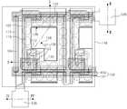
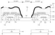
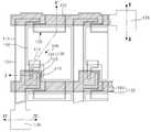
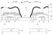
도 3은 본 발명의 실시 예에 따른 반투과형 박막 트랜지스터 기판을 도시한 평면도이고, 도 4는 도 3에 도시된 반투과형 박막 트랜지스터 기판을 Ⅱ-Ⅱ', Ⅲ-Ⅲ', Ⅳ-Ⅳ'선을 따라 절단하여 도시한 단면도이다.3 is a plan view illustrating a transflective thin film transistor substrate according to an exemplary embodiment of the present invention, and FIG. 4 is a line II-II ', III-III', and IV-IV 'of the transflective thin film transistor substrate shown in FIG. It is a cross-sectional view cut along the.
도 3 및 도 4에 도시된 반투과형 박막 트랜지스터 기판은 하부 기판(142) 위에 게이트 절연막(144)을 사이에 두고 교차하여 화소 영역을 정의하는 게이트 라인(102) 및 데이터 라인(104), 그 게이트 라인(102) 및 데이터 라인(104)과 접속된 박막 트랜지스터(106), 각 화소의 반사 영역에 형성된 반사 전극(152), 각 화소 영역에 형성되고 반사 전극(152)을 통해 박막 트랜지스터(106)와 접속된 화소 전극(118)을 구비한다. 그리고, 반투과형 박막 트랜지스터 기판은 반사 전극(152)을 통해 화소 전극(118)에 접속된 스토리지 상부 전극(122)과 전단 게이트 라인(102)의 중첩으로 형성된 스토리지 캐패시터(120), 게이트 라인(102)과 접속된 게이트 패드(128), 데이터 라인(104)과 접속된 데이터 패드(138)를 구비한다. 이러한 반투과형 박막 트랜지스터 기판에서 각 화소 영역은 반사 전극(152)이 형성된 반사 영역과 반사 전극(152)이 형성되지 않은 투과 영역으로 구분된다.3 and 4 may include a
박막 트랜지스터(106)는 게이트 라인(102)과 접속된 게이트 전극(108), 데이터 라인(104)과 접속된 소스 전극(110), 소스 전극(110)과 마주하며 화소 전극(118)과 접속된 드레인 전극(112), 게이트 절연막(144)을 사이에 두고 게이트 전극(108)과 중첩되어 소스 전극(110)과 드레인 전극(112) 사이에 채널을 형성하는 활 성층(114), 소스 전극(110) 및 드레인 전극(112)과의 오믹 접촉을 위하여 채널부를 제외한 활성층(114) 위에 형성된 오믹 접촉층(116)을 구비한다. 이러한 박막 트랜지스터(106)는 게이트 라인(102)의 스캔 신호에 응답하여 데이터 라인(104) 상의 비디오 신호가 화소 전극(118)에 충전되어 유지되게 한다.The
여기서, 게이트 라인(102) 및 게이트 전극(108)은 투명 도전층으로 이루어진 제1 도전층(101)과, 그 위에 금속층으로 이루어진 제2 도전층(103)이 적층된 이중 구조를 갖는다.Here, the
그리고, 활성층(114) 및 오믹 접촉층(116)을 포함하는 반도체 패턴(115)은 데이터 라인(104)과도 중첩되게 형성된다.The
반사 전극(152)은 각 화소의 반사 영역에 형성되어 외부광을 반사시킨다. 이러한 반사 전극(152)은 그 아래의 유기막(148)의 형상을 따라 엠보싱 형상을 갖게 됨으로써 산란 효과로 반사 효율을 증대시킨다. 반사 전극(152)은 제1 및 제2 반사 금속층(151, 153)이 적층된 이중 구조를 갖는다. 제1 반사 금속층(151)은 투명 도전층인 화소 전극(118)과의 컨택 저항을 감소시킬 수 있는 Mo 등과 같은 금속을, 제2 반사 금속층(153)은 AlNd 등과 같이 반사율이 높은 금속을 이용한다.The
화소 전극(118)은 각 화소 영역에 형성되고 투과홀(154)의 에지부를 경유하는 반사 전극(152)을 통해 드레인 전극(112)과 접속된다. 화소 전극(118)은 게이트 라인(102)의 제1 도전층(101)과 같은 투명 도전층으로 형성되고, 투과 영역에서 투과홀(154)을 통해 노출된다. 화소 전극(118)은 박막 트랜지스터를 통해 공급된 화소 신호에 의해 칼라 필터 기판(미도시)의 공통 전극과 전위차를 발생시킨다. 이 전위차에 의해 유전 이방성을 갖는 액정이 회전하여 반사 영역과 투과 영역 각각의 액정층을 경유하는 광의 투과율을 조절하므로 상기 비디오 신호에 따라 휘도가 달라지게 된다.The
투과홀(154)은 투과 영역에서 화소 전극(118) 위의 게이트 절연막(144)과, 박막 트랜지스터(106) 위의 보호막(146), 유기막(148)을 관통하여 형성된다. 이에 따라, 반사 영역과 투과 영역에서 액정층을 경유하는 광 경로의 길이가 동일해지게 되므로 반사 모드와 투과 모드의 투과 효율이 같아지게 된다.The
스토리지 캐패시터(120)는 화소 전극(118)과 접속된 스토리지 상부 전극(122)이 게이트 절연막(144)을 사이에 두고 전단 게이트 라인(102)과 중첩됨으로써 형성된다. 스토리지 상부 전극(122)은 투과홀(154)의 에지부를 경유하는 반사 전극(152)을 통해 화소 전극(118)과 접속되고, 스토리지 상부 전극(122)의 아래에는 반도체 패턴(115)이 더 중첩된다.The
게이트 라인(102)은 게이트 패드(128)를 통해 게이트 드라이버(도시하지 않음)와 접속된다. 게이트 패드(128)는 게이트 라인(102)의 제1 도전층(101)이 연장되어 형성된다.The
데이터 라인(104)은 데이터 패드(138)를 통해 데이터 드라이버(도시하지 않음)와 접속된다. 데이터 패드(138)는 게이트 패드(128)과 같이 제1 도전층(101)으로 형성된다. 이러한 데이터 패드(138)는 별도의 컨택 전극(미도시)를 통해 데이터 라인(104)과 접속된다.The
게이트 패드(128) 및 데이터 패드(138)가 형성된 패드 영역에서는 게이트 절 연막(144), 보호막(146), 유기막(148)이 제거된다.In the pad region in which the
이와 같이, 본 발명의 실시 예에 따른 반투과형 박막 트랜지스터 기판에서는 투과홀(154)의 에지부를 경유하는 반사 전극(152)을 통해 화소 전극(118)이 드레인 전극(112) 및 스토리지 상부 전극(122)과 접속된다. 이에 따라, 화소 전극(118)과 드레인 전극(112) 및 스토리지 상부 전극(122)과의 접속을 위한 별도의 컨택홀이 필요없게 되므로 그 만큼 투과 영역의 개구율을 증대시킬 수 있게 된다.As described above, in the transflective thin film transistor substrate according to the exemplary embodiment of the present invention, the
그리고, 반사 전극(152) 중 투명 도전층과의 컨택 저항이 작은 제1 반사 금속층(151)이 화소 전극(118)과 접속하게 된다. 이에 따라, 제1 반사 금속층(151)으로 Mo를, 제2 반사 금속층(153)으로 AlNd를, 화소 전극(118)으로 ITO를 이용하는 경우 AlNd와 ITO는 Mo을 통해서만 접속하게 되므로 Al2O3생성으로 인한 AlNd와 ITO와의 컨택 저항 증가를 방지할 수 있게 된다.The first
이러한 구성을 갖는 본 발명의 실시 예에 따른 박막 트랜지스터 기판은 다음과 같이 5마스크 공정으로 형성된다.The thin film transistor substrate according to the embodiment of the present invention having such a configuration is formed in a five mask process as follows.
도 5a 및 도 5b는 본 발명의 실시 예에 따른 반투과형 박막 트랜지스터 기판 제조 방법 중 제1 마스크 공정을 설명하기 위한 평면도 및 단면도를, 도 6a 내지 도 6e는 제1 마스크 공정을 구체적으로 설명하기 위한 단면도들을 도시한 것이다.5A and 5B are plan views and cross-sectional views illustrating a first mask process in a method of manufacturing a transflective thin film transistor substrate according to an exemplary embodiment of the present invention, and FIGS. 6A to 6E illustrate the first mask process in detail. Cross-sectional views are shown.
제1 마스크 공정으로 하부 기판(142) 상에 게이트 라인(102), 게이트 라인(102)과 접속된 게이트 전극(108)을 포함하는 게이트 패턴과, 게이트 패드(128), 데이터 패드(138), 화소 전극(118)을 포함하는 투명 도전 패턴이 형성된다. 게이 트 패턴은 제1 및 제2 도전층(101, 103)이 적층된 이중 구조로, 투명 도전 패턴은 게이트 패턴의 제1 도전층(101)과 동일한 단일층으로 형성된다. 이렇게 이중 구조를 갖는 게이트 패턴과, 단일층 구조를 갖는 투명 도전 패턴은 하프 톤(Half Tone) 마스크 또는 회절 마스크를 이용함으로써 하나의 마스크 공정으로 형성된다. 이하에서는 하프 톤 마스크를 이용한 경우만을 예로 들어 설명하기로 한다.A gate pattern including a
구체적으로, 도 6a에 도시된 바와 같이 하부 기판(142) 상에 스퍼터링 방법 등의 증착 방법을 통해 제1 및 제2 도전층(101, 103)이 적층되고, 그 위에 포토레지스트(167)가 형성된다. 제1 도전층(101)으로는 ITO, TO, IZO 등과 같은 투명 도전 물질이, 제2 도전층(103)으로는 Mo, Ti, Cu, Al(Nd)계 등의 금속 물질이 이용된다.Specifically, as shown in FIG. 6A, the first and second
그 다음, 하프 톤 마스크(260)를 이용한 포토리소그래피 공정으로 포토레지스트(167)를 노광 및 현상함으로써 도 6b에 도시된 바와 같이 단차를 갖는 포토레지스트 패턴(168)이 형성된다.Next, the
하프 톤 마스크(260)는 투명한 석영(SiO2; Quartz) 기판(266)과, 그 위에 형성된 차단층(262) 및 부분 투과층(264)을 구비한다. 부분 투과층(264)과 중첩된 차단층(262)은 게이트 패턴이 형성되어질 영역에 위치하여 자외선(UV)을 차단함으로써 현상 후 제1 포토레지스 패턴(268A)이 남게 한다. 차단층(262)과 비중첩된 부분 투과층(264)은 투명 도전 패턴이 형성되어질 영역에 위치하여 자외선(UV)을 부분적으로 투과시킴으로써 현상 후 제1 포토레지스트 패턴(268A) 보다 얇은 제2 포토레지스트 패턴(268B)이 남게 한다. 이를 위하여, 차단층(262)은 Cr, CrOx 등과 같은 금속으로, 부분 투과층(264)은 MoSix 등으로 형성된다.It includes a
이어서, 단차를 갖는 포토레지스트 패턴(268)을 이용한 식각 공정으로 제1 및 제2 도전층(101, 103)을 패터닝함으로써 도 6c에 도시된 바와 같이 이중층 구조의 게이트 패턴과, 위에 제2 도전층(103)이 남아 있는 투명 도전 패턴이 형성된다.Subsequently, the first and second
그 다음, 산소(O2) 플라즈마를 이용한 애싱 공정으로 포토레지스트 패턴(268)을 애싱함으로써 도 6d에 도시된 바와 같이 제1 포토레지스트 패턴(268A)은 두께가 얇아지게 되고, 제2 포토레지스 패턴(268B)은 제거된다. 그리고, 애싱된 제1 포토레지스트 패턴(268A)을 이용한 식각 공정으로 투명 도전 패턴 위의 제2 도전층(103)이 제거된다. 이때, 애싱된 제1 포토레지스트 패턴(268A)을 따라 패터닝된 제2 도전층(103)의 양측부가 한번 더 식각됨으로써 게이트 패턴의 제1 및 제2 도전층(101, 103)은 계단 형태로 일정한 단차를 갖게 된다. 이에 따라, 제1 및 제2 도전층(101, 103)의 측면부가 높은 급경사를 갖게 될 경우 그 위에서 발생될 수 있는 소스/드레인 금속층의 단선 불량을 방지할 수 있게 된다.Next, by ashing the
그리고, 스트립 공정으로 게이트 패턴 위에 잔존하던 제1 포토레지스트 패턴(268A)이 도 6e에 도시된 바와 같이 제거된다.In addition, the
도 7a 및 도 7b는 본 발명의 실시 예에 따른 박막 트랜지스터 기판 제조 방법 중 제2 마스크 공정을 설명하기 위한 평면도 및 단면도를 도시한 것이고, 도 8a 내지 도 8e는 제2 마스크 공정을 구체적으로 설명하기 위하 단면도들을 도시한 것 이다.7A and 7B illustrate a plan view and a cross-sectional view for describing a second mask process in a method of manufacturing a thin film transistor substrate according to an exemplary embodiment of the present invention, and FIGS. 8A to 8E illustrate the second mask process in detail. The cross sections are shown below.
게이트 패턴과 화소 전극(118)이 형성된 하부 기판(142) 상에 게이트 절연막(144)이 형성되고, 그 위에 제2 마스크 공정으로 데이터 라인(104), 소스 전극(110), 드레인 전극(112), 스토리지 상부 전극(122)을 포함하는 소스/드레인 패턴과, 소스/드레인 패턴의 배면을 따라 중첩된 활성층(114) 및 오믹 접촉층(116)을 포함하는 반도체 패턴(115)이 형성된다. 이러한 반도체 패턴(115)과 소스/드레인 패턴은 회절 노광 마스크를 이용한 하나의 마스크 공정으로 형성된다.A
구체적으로, 도 8a와 같이 게이트 패턴이 형성된 하부 기판(142) 상에 게이트 절연막(144), 비정질 실리콘층(105), 불순물(n+ 또는 p+)이 도핑된 비정질 실리콘층(107), 소스/드레인 금속층(109)이 순차적으로 형성된다. 예를 들면, 게이트 절연막(144), 비정질 실리콘층(105), 불순물이 도핑된 비정질 실리콘층(107)은 PECVD 방법으로, 소스/드레인 금속층(109)은 스퍼터링 방법으로 형성된다. 게이트 절연막(144)으로는 산화 실리콘(SiOx), 질화 실리콘(SiNx) 등과 같은 무기 절연 물질이, 소스/드레인 금속층(109)으로는 Cr, Mo, MoW, Al/Cr, Cu, Al(Nd), Al/Mo, Al(Nd)/Al, Al(Nd)/Cr, Mo/Al(Nd)/Mo, Cu/Mo, Ti/Al(Nd)/Ti 등이 이용되며, 이중층인 예를 들면 Al/Cr인 경우 Cr을 먼저 형성한 후에 Al을 형성하는 것을 말한다.Specifically, as shown in FIG. 8A, the
그리고, 소스/드레인 금속층(109) 위에 포토레지스트(219)가 도포된 다음, 회절 노광 마스크(210)을 이용한 포토리소그래피 공정으로 포토레지스트(219)를 노광 및 현상함으로써 도 8b에 도시된 바와 같이 단차를 갖는 포토레지스트 패턴(220)이 형성된다.Then, the
회절 노광 마스크(210)는 투명한 석영 기판(212)과, 그 위에 Cr, CrOx 등과 같은 금속층으로 형성된 차단층(214) 및 회절 노광용 슬릿(216)을 구비한다. 차단층(214)은 반도체 패턴 및 소스/드레인 패턴이 형성되어질 영역에 위치하여 자외선을 차단함으로써 현상 후 제1 포토레지스트 패턴(220A)이 남게 한다. 회절 노광용 슬릿(216)은 박막 트랜지스터의 채널이 형성될 영역에 위치하여 자외선을 회절시킴으로써 현상 후 제1 포토레지스트 패턴(220A) 보다 얇은 제2 포토레지스트 패턴(220B)이 남게 한다.The
이어서, 단차를 갖는 포토레지스트 패턴(220)을 이용한 식각 공정으로 소스/드레인 금속층(105)이 패터닝됨으로써 도 8c에 도시된 바와 같이 소스/드레인 패턴과, 그 아래의 반도체 패턴(115)이 형성된다. 이 경우, 소스/드레인 패턴 중 소스 전극(110)과 드레인 전극(112)은 일체화된 구조를 갖는다.Subsequently, the source /
그 다음, 산소(O2) 플라즈마를 이용한 애싱 공정으로 포토레지스트 패턴(220)을 애싱함으로써 도 8d에 도시된 바와 같이 제1 포토레지스트 패턴(220A)은 얇아지게 되고, 제2 포토레지스트 패턴(220B)은 제거된다. 그리고, 애싱된 제1 포토레지스트 패턴(220A)을 이용한 식각 공정으로 제2 포토레지스트 패턴(220B)의 제거로 노출된 소스/드레인 패턴과, 그 아래의 오믹 접촉층(116)이 제거됨으로써 소스 전극(110)과 드레인 전극(112)은 분리되고 활성층(114)이 노출된다. 이에 따라, 소스 전극(110)과 드레인 전극(112) 사이에는 활성층(114)으로 이루어진 채널이 형성된다. 이때, 애싱된 제1 포토레지스트 패턴(220A)을 따라 소스/드레인 패 턴의 양측부가 한번 더 식각됨으로써 소스/드레인 패턴과 반도체 패턴(115)은 계단 형태로 일정한 단차를 갖게 된다.Then, by ashing the
그리고, 스트립 공정으로 소스/드레인 패턴 위에 잔존하던 제1 포토레지스트 패턴(220A)이 도 8e와 같이 제거된다.Then, the
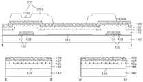
도 9a 및 도 9b는 본 발명의 실시 예에 따른 박막 트랜지스터 기판 제조 방법 중 제3 마스크 공정을 설명하기 위한 평면도 및 단면도고, 도 10a 내지 도 10c는 제3 마스크 공정을 단계적으로 설명하기 위한 단면도들이다.9A and 9B are plan and cross-sectional views illustrating a third mask process in a method of manufacturing a thin film transistor substrate according to an exemplary embodiment of the present invention, and FIGS. 10A through 10C are cross-sectional views illustrating a third mask process step by step. .
제3 마스크 공정으로 소스/드레인 패턴이 형성된 게이트 절연막(144) 상에 투과 영역에서 투과홀(154)을 갖는 보호막(146) 및 유기막(148)이 형성된다.The
도 10a를 참조하면, 소스/드레인 패턴이 형성된 게이트 절연막(144) 상에 PECVD 등의 증착 방법으로 보호막(146)이 형성된다. 보호막(146)으로는 게이트 절연막(144)과 같은 무기 절연 물질이 이용된다.Referring to FIG. 10A, a
도 10b를 참조하면, 반사 영역에서 엠보싱 표면을 갖고 투과 영역에서 투과홀(154)을 갖는 유기막(148)이 보호막(146) 위에 형성된다.Referring to FIG. 10B, an
구체적으로, 유기막(148)은 아크릴 등과 같은 감광성 유기 물질을 스핀 코팅 방법 등으로 보호막(146) 위에 코팅함으로써 형성된다. 그 다음, 제3 마스크를 이용한 포토리소그래피 공정으로 유기막(148)을 패터닝함으로써 제3 마스크의 투과부에 대응하여, 투과 영역에서 유기막(148)을 관통하는 투과홀(154)가 형성되고 게이트 패드(128) 및 데이터 패드(138)가 형성된 패드 영역의 유기막(148)이 제거된다. 또한, 제3 마스크에서 투과부를 제외한 나머지 부분이 차단부와 회절 노광부(또는 반투과부)가 반복되는 구조를 갖게 되고, 이에 대응하여 유기막(148)은 반사 영역에서 단차를 갖는 차단 영역(돌출부) 및 회절 노광 영역(홈부)이 반복되는 구조로 패터닝된다. 이어서, 돌출부 및 홈부가 반복된 유기막(148)을 소성함으로써 반사 영역에서 유기막(148)의 표면은 엠보싱 형상을 갖게 된다.Specifically, the
도 10c를 참조하면, 유기막(148)을 마스크로 이용하여 그 아래의 보호막(146) 및 게이트 절연막(144)을 패터닝함으로써 투과홀(154)은 게이트 절연막(144)까지 관통하게 되고, 패드 영역의 보호막(146) 및 게이트 절연막(144)이 제거된다. 이 경우, 투과홀(154)을 통해 노출된 드레인 전극(112) 및 스토리지 상부 전극(122)과 그 아래의 반도체 패턴(115)도 식각된다. 여기서, 식각 속도 차이로 인하여 드레인 전극(112) 및 스토리지 상부 전극(122)과 그 아래의 반도체 패턴(115) 보다 게이트 절연막(144)의 에지부가 약간 돌출된 구조를 갖게 된다. 이러한 투과홀(154)은 화소 전극(118)의 제2 도전층(103)을 노출시키고, 그의 에지부는 드레인 전극(112) 및 스토리지 상부 전극(122)의 측면을 노출시킨다.Referring to FIG. 10C, the
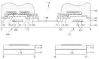
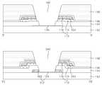
도 11a 및 도 11b는 본 발명의 실시 예에 따른 박막 트랜지스터 기판 제조 방법 중 제4 마스크 공정을 설명하기 위한 평면도 및 단면도를 도시한 것이다.11A and 11B illustrate a plan view and a cross-sectional view for describing a fourth mask process in a method of manufacturing a thin film transistor substrate according to an exemplary embodiment of the present invention.
제4 마스크 공정으로 각 화소의 반사 영역에 반사 전극(152)이 형성된다.The
구체적으로, 엠보싱 표면을 갖는 유기막(148) 위에 반사 금속층이 엠보싱 형상을 유지하며 형성된다. 반사 금속층은 Mo 등과 같이 화소 전극(118)과의 컨택 저항이 작은 제1 반사 금속층(151)과, AlNd 등과 같이 반사율이 높은 제2 반사 금속층(153)이 적층된 이중 구조로 형성된다. 이어서, 제5 마스크를 이용한 포토리 소그래피 공정 및 식각 공정으로 제1 및 제2 반사 금속층(151, 152)이 패터닝됨으로써 각 화소의 반사 영역마다 반사 전극(152)이 형성된다. 이러한 반사 전극(152)은 투과홀(154)의 에지부를 경유하여 드레인 전극(112)과 화소 전극(118)을 접속시키고, 스토리지 상부 전극(122)과 화소 전극(118)을 접속시키게 된다. 이에 따라, 화소 전극(118)과 드레인 전극(112) 및 스토리지 상부 전극(122)과의 접속을 위한 별도의 컨택홀이 필요없게 되므로 투과 영역의 개구율을 증대시킬 수 있게 된다. 또한, 반사 전극(152) 중 제1 반사 금속층(151)이 투명 도전층인 화소 전극(118)과 접속되므로 컨택 저항을 감소시킬 수 있게 된다.Specifically, a reflective metal layer is formed on the
이와 같이, 본 발명의 실시 예에 따른 반투과형 박막 트랜지스터 기판의 제조 방법은 화소 전극(118)을 하프 톤 또는 회절 마스크를 이용하여 게이트 패턴과 같이 형성하고, 반사 전극(152)으로 화소 전극(118)과 드레인 전극(112) 및 스토리지 상부 전극(122)을 접속시킴으로써 하나의 마스크 공정을 줄일 수 있게 된다.As described above, in the method of manufacturing the transflective thin film transistor substrate according to the exemplary embodiment of the present invention, the
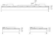
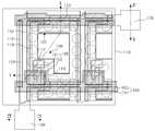
도 12는 본 발명의 실시 예에 따른 반투과형 박막 트랜지스터 기판의 주변부를 개략적으로 도시한 것이다.12 schematically illustrates a periphery of a transflective thin film transistor substrate according to an embodiment of the present invention.
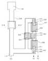
도 12에 도시된 반투과형 박막 트랜지스터 기판(100)은 게이트 패드(128)와 동일층에 형성된 데이터 패드(138)를 데이터 라인(104)과 접속시키기 위한 컨택 전극(160)을 구비한다. 다시 말하여, 컨택 전극(160)은 데이터 패드(138)로부터 신장된 데이터 링크(136)과 데이터 라인(104)을 접속시킨다. 여기서, 컨택 전극(160)은 액티브 영역(182)에 형성되는 반사 전극(152)과 동일한 금속층(AlNd, AlNd/Mo)으로 형성하기로 한다. 이러한 컨택 전극(160)은 외부로 노출되는 경우 산화 작용 으로 부식되는 문제가 있으므로 실링재(180)에 의해 밀봉되는 영역, 즉 실링재(180)와 액티브 영역(182) 사이에 위치하여 부식을 방지할 수 있다.The transflective thin
또한, 박막 트랜지스터 기판(100)은 액티브 영역(182)으로 유입되는 정전기를 차단하기 위한 정전기 방지 소자(190)를 구비한다. 정전기 방지 소자(190)는 데이터 라인(104) 또는 게이트 라인(102)과 접속되며 상호 접속 관계를 갖는 다수개의 박막 트랜지스터들(300, 310, 320)로 구성된다. 정전기 방지 소자(190)는 정전기 등에 의한 고전압 영역에서는 낮은 임피던스를 가져 과전류가 방전되게 함으로써 정전기 유입을 차단하고, 정상적인 구동환경에서는 높은 임피던스를 가져 데이터 라인(104) 또는 게이트 라인(102)을 통해 공급되는 구동 신호에는 영향을 주지 않게 한다. 이러한 정전기 방지 소자(190)는 박막 트랜지스터들(300, 310, 320)을 상호 접속시키기 위하여 다수의 컨택 전극들을 필요로 한다. 이러한 다수의 컨택 전극들도 반사 전극(152)과 동일한 금속층(AlNd, AlNd/Mo)으로 형성하기로 한다. 이에 따라, 정전기 방지 소자(190)도 실링재(180)에 의해 밀봉되는 영역, 즉 실링재(180)와 액티브 영역(182) 사이에 형성된다.In addition, the thin
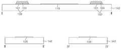
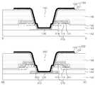
도 13은 도 12에 도시된 데이터 라인(104)과 접속된 컨택 전극(160) 및 정전기 방지 소자(190)를 구체적으로 도시한 평면도이고, 도 14는 도 13에 도시된 박막 트랜지스터 기판을 Ⅴ-Ⅴ', Ⅵ-Ⅵ'선을 따라 절단하여 도시한 단면도이다.FIG. 13 is a plan view specifically illustrating a
도 13 및 도 14에 도시된 데이터 링크(136)는 데이터 패드(138)로부터 연장되어 실링재(180)로 밀봉되어질 영역에 위치하는 데이터 라인(104)의 끝부분과 중첩된다. 데이터 링크(136)는 데이터 패드(138)와 동일하게 제1 도전층(101)인 투 명 도전층으로만 형성된다.The data link 136 shown in FIGS. 13 and 14 overlaps the end of the
제1 컨택 전극(160)은 데이터 링크(136)과 데이터 라인(104)의 중첩부에 형성된 제1 컨택홀(162)에 걸쳐 형성되어 데이터 라인(104) 및 데이터 링크(136)를 접속시킨다. 제1 컨택홀(162)은 유기막(148)으로부터 보호막(146), 데이터 라인(104), 반도체 패턴(115), 게이트 절연막(144)까지 관통하여 데이터 링크(136)를 노출시킨다. 이에 따라, 제1 컨택 전극(160)은 제1 컨택홀(162)을 통해 노출된 데이터 라인(104)과 측면 접속되고, 데이터 링크(136)와는 면 접속하게 된다.The
데이터 라인(104)과 접속된 정전기 방지 소자는 제2 내지 제4 박막 트랜지스터(300, 310, 320)를 구비한다.The antistatic device connected to the
제2 박막 트랜지스터(300)는 데이터 라인(104)과 접속된 제2 소스 전극(304)과, 그 제2 소스 전극(304)과 대향된 제2 드레인 전극(306)과, 제2 소스 및 드레인 전극(304, 306)과 반도체 패턴(115) 및 게이트 절연막(144)을 사이에 두고 중첩된 제2 게이트 전극(302)을 구비한다. 여기서, 제2 게이트 전극(302)은 제1 및 제2 도전층(101, 103)의 이중 구조를 갖는다.The second
제3 박막 트랜지스터(310)는 제2 박막 트랜지스터의 제2 소스 전극(304)과 제2 게이트 전극(302) 사이에 다이오드형으로 접속된다. 이를 위하여, 제3 박막 트랜지스터(310)는 상기 제2 소스 전극(304)과 접속된 제3 소스 전극(314)과, 그 제3 소스 전극(314)과 대향된 제3 드레인 전극(316)과, 그 제3 소스 및 드레인 전극(314, 316)과 반도체 패턴(115) 및 게이트 절연막(144)을 사이에 두고 중첩된 제3 게이트 전극(312)을 구비한다. 여기서, 제3 게이트 전극(322)은 제1 및 제2 도 전층(101, 103)의 이중 구조를 갖는다. 그리고, 제3 게이트 전극(312)은 제2 컨택홀(340)에 걸쳐 형성된 제2 컨택 전극(332)을 통해 제3 소스 전극(314)과 접속된다. 제2 컨택홀(340)은 유기막(148), 보호막(146), 제3 소스 전극(314), 반도체 패턴(115), 게이트 절연막(144), 제3 게이트 전극(312)의 제2 도전층(103)을 관통하여 제3 게이트 전극(312)의 제1 도전층(101)을 노출시킨다.The third
제4 박막 트랜지스터(320)는 상기 제2 박막 트랜지스터의 제2 드레인 전극(306)과 제2 게이트 전극(302) 사이에 다이오드형으로 접속된다. 이를 위하여, 제4 박막 트랜지스터(320)는 상기 제2 드레인 전극(306)과 접속된 제4 소스 전극(324)과, 그 제4 소스 전극(324)과 대향된 제4 드레인 전극(326)과, 그 제4 소스 및 드레인 전극(324, 326)과 반도체 패턴(115) 및 게이트 절연막(144)을 사이에 두고 중첩된 제4 게이트 전극(322)을 구비한다. 여기서, 제4 게이트 전극(322)은 제1 및 제2 도전층(101, 103)의 이중 구조를 갖는다. 제4 드레인 전극(326)은 제3 드레인 전극(316)과 접속되며, 제3 컨택홀(344)에 걸쳐 형성된 제3 컨택 전극(334)을 통해 제2 게이트 전극(302)과 접속된다. 또한, 제4 게이트 전극(322)은 제4 컨택홀(348)에 걸쳐 형성된 제4 컨택 전극(336)을 통해 제4 소스 전극(324)과 접속된다. 제3 컨택홀(344)은 유기막(148), 보호막(146), 제4 드레인 전극(326), 반도체 패턴(115), 게이트 절연막(144), 제2 게이트 전극(302)의 제1 도전층(103)을 관통하여 형성되고, 제4 컨택홀(348)은 유기막(148), 보호막(146), 제4 소스 전극(324), 반도체 패턴(115), 게이트 절연막(144), 제4 게이트 전극(322)의 제1 도전층(103)을 관통하여 형성된다.The fourth
여기서, 제1 내지 제4 컨택 전극(160, 332, 334, 336)은 전술한 바와 같이 반사 전극(152)과 동일하게 제1 및 제2 반사 금속층(151, 152)이 적층된 이중 구조를 갖는다. 이에 따라, 제1 내지 제4 컨택 전극(160, 332, 334, 336)의 제1 반사 금속층(151)이 투명 도전층인 제1 도전층(103)과 접속하므로 컨택 저항을 감소시킬 수 있게 된다.Here, the first to
이러한 구조를 갖는 반투과형 박막 트랜지스터 기판은 전술한 바와 같이 5마스크 공정으로 형성한다. 이를 도 15a 내지 도 19b를 참조하여 설명하기로 한다.The semi-transmissive thin film transistor substrate having this structure is formed in a five mask process as described above. This will be described with reference to FIGS. 15A to 19B.
도 15a 및 도 15b를 참조하면, 제1 마스크 공정으로 하부 기판(142) 상에 데이터 패드(138)과 함께 데이터 링크(136), 제2 내지 제4 게이트 전극(302, 312, 322)을 포함하는 게이트 패턴이 형성된다. 여기서, 데이터 패드(138) 및 데이터 링크(136)는 제1 도전층(101)인 투명 도전층으로만 형성되고, 제2 내지 제4 게이트 전극(302, 312, 322)을 포함하는 게이트 패턴은 제1 및 제2 도전층(101, 103)이 적층된 이중 구조를 갖는다. 이러한 제1 마스크 공정은 도 5a 내지 도 6e에서 전술한 바와 같이 하프 톤 마스크(또는 회절 마스크)를 이용한다.15A and 15B, the first mask process includes a
도 16a 및 도 16b를 참조하면, 제2 마스크 공정으로 게이트 절연막(144)과, 활성층(114) 및 오믹 접촉층(116)을 포함하는 반도체 패턴(115)과, 데이터 라인(104), 제2 내지 제4 소스 전극(304, 314, 324), 제2 내지 제4 드레인 전극(306, 316, 326)을 포함하는 소스/드레인 패턴이 형성된다. 이러한 제2 마스크 공정은 도 7a 내지 도 8e에서 전술한 바와 같다.16A and 16B, a
도 17a 및 도 17b를 참조하면, 제3 마스크 공정으로 보호막(146) 및 유기막 (148)이 형성되고, 유기막(148)에서 게이트 절연막(144)까지 관통하는 제1 컨택홀(162)과, 제2 내지 제3 게이트 전극의 제2 도전층(103)까지 관통하는 제2 내지 제4 컨택홀(340, 344, 348)이 형성된다. 이러한 제3 마스크 공정은 도 9a 내지 도 10c에서 전술한 바와 같다. 이 경우, 유기막(148)은 패드 영역에서는 제거되고, 화소 영역과 같이 반사 전극(152)이 형성되지 않는 부분에서는 엠보싱 표면을 갖지 않는다.17A and 17B, a
도 18a 및 도 18b를 참조하면, 제4 마스크 공정으로 반사 전극(152)과 동일한 이중 구조의 제1 내지 제4 컨택 전극(160, 332, 334, 336)이 형성된다. 이러한 제4 마스크 공정은 도 11a 및 도 11b에서 전술한 바와 같다.
18A and 18B, the first to
상술한 바와 같이, 본 발명에 따른 반투과형 박막 트랜지스터 기판 및 그 제조 방법은 이중 구조의 게이트 패턴과, 단일층 구조의 투명 도전 패턴을 하프 톤 마스크(또는 회절 마스크)를 이용하여 하나의 마스크 공정으로 형성함으로써 공정을 단순화할 수 있게 된다. 또한, 하프 톤 마스크(또는 회절 마스크) 공정으로 이중 구조 게이트 패턴의 제1 및 제2 도전층이 계단 형태로 일정한 단차를 갖게 되므로 제1 및 제2 도전층의 급경사로 인한 소스/드레인 패턴의 단선을 방지할 수 있게 된다.As described above, the semi-transmissive thin film transistor substrate according to the present invention and a method of manufacturing the same are used in one mask process by using a half-tone mask (or a diffraction mask) by using a gate pattern having a double structure and a transparent conductive pattern having a single layer structure. By forming, the process can be simplified. In addition, the half-tone mask (or diffraction mask) process causes the first and second conductive layers of the double-structured gate pattern to have a constant step in the form of a step, so that the disconnection of the source / drain pattern due to the steep slope of the first and second conductive layers is caused. Can be prevented.
또한, 본 발명에 따른 반투과형 박막 트랜지스터 기판 및 그 제조 방법은 유기막 패터닝시 화소 전극을 노출시키는 투과홀을 형성하고, 투과홀의 에지부를 경 유하는 반사 전극으로 드레인 전극 및 스토리지 상부 전극을 화소 전극과 접속시키게 된다. 이에 따라, 공정을 더 단순화할 수 있을 뿐만 아니라, 드레인 전극 및 스토리지 상부 전극을 화소 전극과 접속시키기 위한 별도의 컨택홀들이 필요없게 되므로 그 만큼 투과 영역의 개구율을 증대시킬 수 있게 된다.In addition, the semi-transmissive thin film transistor substrate and the method of manufacturing the same according to the present invention form a through hole that exposes the pixel electrode when the organic layer is patterned, and the drain electrode and the storage upper electrode as the reflective electrode through the edge portion of the through hole pixel electrode Connected with. As a result, the process can be further simplified, and the contact ratios for connecting the drain electrode and the storage upper electrode to the pixel electrode are not required, thereby increasing the aperture ratio of the transmission region.
또한, 본 발명에 따른 반투과형 박막 트랜지스터 기판 및 그 제조 방법은 반사 전극과 동일한 금속의 컨택 전극으로 서로 다른 층에 형성된 데이터 링크 및 데이터 라인을 접속시키고, 정전기 방지 소자의 박막 트랜지스터들을 상호 접속시키게 된다. 이에 따라, 4마스크 공정으로 공정을 단순화할 수 있게 된다.In addition, the semi-transmissive thin film transistor substrate and the method of manufacturing the same according to the present invention connect the data link and the data line formed in different layers with the contact electrode of the same metal as the reflective electrode, and interconnect the thin film transistors of the antistatic element. . Accordingly, the process can be simplified to a four mask process.
더불어, 본 발명에 따른 반투과형 박막 트랜지스터 기판 및 그 제조 방법은 반사 전극 및 컨택 전극을 이중 구조로 형성하고, 저 컨택 저항을 갖는 제1 반사 금속층이 투명 도전층과 접속되게 함으로써 컨택 저항을 더 감소시킬 수 있게 된다.In addition, the semi-transmissive thin film transistor substrate and the method of manufacturing the same according to the present invention further reduce the contact resistance by forming the reflective electrode and the contact electrode in a double structure and allowing the first reflective metal layer having a low contact resistance to be connected with the transparent conductive layer. You can do it.
이상 설명한 내용을 통해 당업자라면 본 발명의 기술사상을 일탈하지 아니하는 범위에서 다양한 변경 및 수정이 가능함을 알 수 있을 것이다. 따라서, 본 발명의 기술적 범위는 명세서의 상세한 설명에 기재된 내용으로 한정되는 것이 아니라 특허 청구의 범위에 의해 정하여져야만 할 것이다.Those skilled in the art will appreciate that various changes and modifications can be made without departing from the technical spirit of the present invention. Therefore, the technical scope of the present invention should not be limited to the contents described in the detailed description of the specification but should be defined by the claims.
Claims (17)
Translated fromKoreanPriority Applications (5)
| Application Number | Priority Date | Filing Date | Title |
|---|---|---|---|
| KR1020040041143AKR101116816B1 (en) | 2004-06-05 | 2004-06-05 | Thin Film Transistor Substrate of Transflective Type And Method for Fabricating The Same |
| CN2005100748193ACN100407035C (en) | 2004-06-05 | 2005-06-03 | Liquid crystal display device and manufacturing method thereof |
| US11/143,658US7760309B2 (en) | 2004-06-05 | 2005-06-03 | Transflective liquid crystal display device and fabricating method thereof |
| JP2005165711AJP4268956B2 (en) | 2004-06-05 | 2005-06-06 | Liquid crystal display device and manufacturing method thereof |
| US12/756,319US8072565B2 (en) | 2004-06-05 | 2010-04-08 | Transflective liquid crystal display device |
Applications Claiming Priority (1)
| Application Number | Priority Date | Filing Date | Title |
|---|---|---|---|
| KR1020040041143AKR101116816B1 (en) | 2004-06-05 | 2004-06-05 | Thin Film Transistor Substrate of Transflective Type And Method for Fabricating The Same |
Publications (2)
| Publication Number | Publication Date |
|---|---|
| KR20050115748A KR20050115748A (en) | 2005-12-08 |
| KR101116816B1true KR101116816B1 (en) | 2012-02-28 |
Family
ID=35448478
Family Applications (1)
| Application Number | Title | Priority Date | Filing Date |
|---|---|---|---|
| KR1020040041143AExpired - LifetimeKR101116816B1 (en) | 2004-06-05 | 2004-06-05 | Thin Film Transistor Substrate of Transflective Type And Method for Fabricating The Same |
Country Status (4)
| Country | Link |
|---|---|
| US (2) | US7760309B2 (en) |
| JP (1) | JP4268956B2 (en) |
| KR (1) | KR101116816B1 (en) |
| CN (1) | CN100407035C (en) |
Families Citing this family (37)
| Publication number | Priority date | Publication date | Assignee | Title |
|---|---|---|---|---|
| KR101043675B1 (en)* | 2004-06-05 | 2011-06-22 | 엘지디스플레이 주식회사 | Semi-transmissive thin film transistor substrate and manufacturing method thereof |
| KR101057779B1 (en) | 2004-06-05 | 2011-08-19 | 엘지디스플레이 주식회사 | Semi-transmissive thin film transistor substrate and manufacturing method thereof |
| KR100742376B1 (en)* | 2005-09-30 | 2007-07-24 | 삼성에스디아이 주식회사 | Pad part and manufacturing method thereof |
| KR101305069B1 (en)* | 2005-12-19 | 2013-09-11 | 삼성디스플레이 주식회사 | Array substrate , method of manufacturing the same and display panel having the same |
| KR20070070382A (en)* | 2005-12-29 | 2007-07-04 | 엘지.필립스 엘시디 주식회사 | Array substrate for liquid crystal display device and manufacturing method thereof |
| KR101338613B1 (en)* | 2006-12-28 | 2013-12-06 | 엘지디스플레이 주식회사 | Thin film transistor array substrate and method for fabricating thereof |
| CN101561604B (en)* | 2008-04-17 | 2011-07-06 | 北京京东方光电科技有限公司 | TFT-LCD array substrate structure and manufacturing method thereof |
| JP5536986B2 (en) | 2008-04-30 | 2014-07-02 | 三菱電機株式会社 | Liquid crystal display |
| WO2010029865A1 (en)* | 2008-09-12 | 2010-03-18 | Semiconductor Energy Laboratory Co., Ltd. | Display device |
| CN102160103B (en) | 2008-09-19 | 2013-09-11 | 株式会社半导体能源研究所 | Display device |
| KR101803264B1 (en)* | 2008-09-19 | 2017-12-28 | 가부시키가이샤 한도오따이 에네루기 켄큐쇼 | Semiconductor device |
| EP2172977A1 (en) | 2008-10-03 | 2010-04-07 | Semiconductor Energy Laboratory Co., Ltd. | Display device |
| KR101652693B1 (en) | 2008-10-03 | 2016-09-01 | 가부시키가이샤 한도오따이 에네루기 켄큐쇼 | Display device |
| CN101719493B (en) | 2008-10-08 | 2014-05-14 | 株式会社半导体能源研究所 | Display device |
| TWI383232B (en)* | 2009-03-19 | 2013-01-21 | Au Optronics Corp | Thin film transistor array substrate |
| DE102010003121A1 (en)* | 2010-03-22 | 2011-09-22 | Osram Opto Semiconductors Gmbh | Organic light-emitting device with homogeneous luminance distribution |
| TWM406261U (en)* | 2010-12-01 | 2011-06-21 | Chunghwa Picture Tubes Ltd | Pixel structure and display panel |
| KR101833235B1 (en) | 2011-07-14 | 2018-04-16 | 삼성디스플레이 주식회사 | Thin-film transistor array substrate, organic light emitting display device comprising the same and manufacturing method of the same |
| WO2014013958A1 (en) | 2012-07-20 | 2014-01-23 | Semiconductor Energy Laboratory Co., Ltd. | Display device |
| KR20240138123A (en) | 2012-07-20 | 2024-09-20 | 가부시키가이샤 한도오따이 에네루기 켄큐쇼 | Display device and electronic device including the display device |
| KR102061764B1 (en)* | 2013-07-31 | 2020-01-03 | 엘지디스플레이 주식회사 | Electrostatic discharge circuit and display device having thereof |
| KR102131191B1 (en)* | 2013-09-30 | 2020-07-08 | 엘지디스플레이 주식회사 | Array substrate for fringe field switching mode liquid crystal display device and Method of fabricating the same |
| US9923163B2 (en)* | 2013-12-03 | 2018-03-20 | Oledworks Gmbh | Current distribution in an organic light emitting diode device |
| KR102136638B1 (en)* | 2014-03-31 | 2020-07-22 | 엘지디스플레이 주식회사 | Liquid crystal display apparatus |
| KR20150137218A (en)* | 2014-05-28 | 2015-12-09 | 삼성디스플레이 주식회사 | Liquid crystal display device and method for manufacturing the same |
| TWI566409B (en)* | 2014-08-26 | 2017-01-11 | 元太科技工業股份有限公司 | Transistor and manufacturing method thereof |
| CN104409483B (en)* | 2014-10-16 | 2017-11-14 | 京东方科技集团股份有限公司 | Array base palte and its manufacture method, display device |
| CN105070684B (en)* | 2015-07-17 | 2018-01-05 | 京东方科技集团股份有限公司 | Preparation method of array substrate, array substrate and display device |
| CN105070727B (en)* | 2015-08-21 | 2019-01-15 | 京东方科技集团股份有限公司 | A kind of thin-film transistor array base-plate, its production method and display device |
| CN105204257B (en)* | 2015-11-05 | 2018-10-12 | 京东方科技集团股份有限公司 | A kind of ESD protection locations, array substrate, liquid crystal display panel and display device |
| KR102556023B1 (en)* | 2016-02-26 | 2023-07-17 | 삼성디스플레이 주식회사 | Photosensitive thin film device and apparatus for sensing biometric information including the same |
| KR102373440B1 (en) | 2017-03-17 | 2022-03-14 | 삼성디스플레이 주식회사 | Display panel and display apparatus comprising the same |
| KR102373443B1 (en)* | 2017-09-14 | 2022-03-14 | 삼성디스플레이 주식회사 | Display device |
| JP6732829B2 (en)* | 2018-03-29 | 2020-07-29 | 株式会社Joled | Semiconductor device and display device |
| CN109273500A (en)* | 2018-09-21 | 2019-01-25 | 京东方科技集团股份有限公司 | OLED display substrate, display device and manufacturing method |
| US10852603B2 (en)* | 2019-02-04 | 2020-12-01 | Omnivision Technologies, Inc. | LCOS pixel film layer design for reflection rate improvement |
| CN114078834B (en)* | 2020-08-17 | 2025-02-18 | 深超光电(深圳)有限公司 | Electrostatic protection structure, thin film transistor substrate and display panel |
Citations (3)
| Publication number | Priority date | Publication date | Assignee | Title |
|---|---|---|---|---|
| KR20010087658A (en)* | 2000-03-08 | 2001-09-21 | 윤종용 | A reflective-transmissive complex type TFT LCD and A Method of forming it |
| JP2002107762A (en)* | 2000-10-02 | 2002-04-10 | Sharp Corp | Manufacturing method of matrix substrate for liquid crystal |
| KR20040041491A (en)* | 2002-11-11 | 2004-05-17 | 엘지.필립스 엘시디 주식회사 | method for fabricating of an array substrate for a liquid crystal display device |
Family Cites Families (25)
| Publication number | Priority date | Publication date | Assignee | Title |
|---|---|---|---|---|
| JPS62285464A (en)* | 1986-06-03 | 1987-12-11 | Matsushita Electric Ind Co Ltd | Thin-film transistor array substrate and manufacture thereof |
| US5162933A (en) | 1990-05-16 | 1992-11-10 | Nippon Telegraph And Telephone Corporation | Active matrix structure for liquid crystal display elements wherein each of the gate/data lines includes at least a molybdenum-base alloy layer containing 0.5 to 10 wt. % of chromium |
| KR940004322B1 (en) | 1991-09-05 | 1994-05-19 | 삼성전자 주식회사 | Liquid crystal display devices |
| US5317433A (en) | 1991-12-02 | 1994-05-31 | Canon Kabushiki Kaisha | Image display device with a transistor on one side of insulating layer and liquid crystal on the other side |
| JPH06235939A (en)* | 1993-02-12 | 1994-08-23 | Hitachi Ltd | Liquid crystal display device and manufacturing method thereof |
| DE4339721C1 (en) | 1993-11-22 | 1995-02-02 | Lueder Ernst | Method for producing a matrix of thin-film transistors |
| JP2674516B2 (en)* | 1994-07-21 | 1997-11-12 | 日本電気株式会社 | Active matrix substrate and manufacturing method thereof |
| TW321731B (en) | 1994-07-27 | 1997-12-01 | Hitachi Ltd | |
| JP2639356B2 (en)* | 1994-09-01 | 1997-08-13 | 日本電気株式会社 | Method for manufacturing thin film transistor |
| JP3866783B2 (en) | 1995-07-25 | 2007-01-10 | 株式会社 日立ディスプレイズ | Liquid crystal display |
| KR0156202B1 (en) | 1995-08-22 | 1998-11-16 | 구자홍 | LCD and its manufacturing method |
| JPH09113931A (en) | 1995-10-16 | 1997-05-02 | Sharp Corp | Liquid crystal display |
| JP3072707B2 (en)* | 1995-10-31 | 2000-08-07 | インターナショナル・ビジネス・マシーンズ・コーポレ−ション | Liquid crystal display device and method of manufacturing the same |
| JP3625598B2 (en) | 1995-12-30 | 2005-03-02 | 三星電子株式会社 | Manufacturing method of liquid crystal display device |
| US6043971A (en)* | 1998-11-04 | 2000-03-28 | L.G. Philips Lcd Co., Ltd. | Electrostatic discharge protection device for liquid crystal display using a COG package |
| KR100372579B1 (en)* | 2000-06-21 | 2003-02-17 | 엘지.필립스 엘시디 주식회사 | A method for fabricating array substrate for liquid crystal display device and the same |
| US6620655B2 (en)* | 2000-11-01 | 2003-09-16 | Lg.Phillips Lcd Co., Ltd. | Array substrate for transflective LCD device and method of fabricating the same |
| KR100386849B1 (en)* | 2001-07-10 | 2003-06-09 | 엘지.필립스 엘시디 주식회사 | Circuit for electro static dischrging of tft-lcd |
| TW508830B (en)* | 2001-08-28 | 2002-11-01 | Hannstar Display Corp | Thin film transistor structure having four procedures of mask processing and the manufacturing method |
| TW562962B (en)* | 2002-01-15 | 2003-11-21 | Chi Mei Optoelectronics Corp | Liquid crystal display device |
| KR100456151B1 (en)* | 2002-04-17 | 2004-11-09 | 엘지.필립스 엘시디 주식회사 | Thin film transistor array substrate and method of manufacturing the same |
| US6876416B2 (en)* | 2002-04-30 | 2005-04-05 | Samsung Electronics Co., Ltd. | Liquid crystal display apparatus having alignment film and method of manufacturing the same |
| JP4035094B2 (en)* | 2002-07-31 | 2008-01-16 | エルジー.フィリップス エルシーデー カンパニー,リミテッド | Reflective transmission type liquid crystal display device and manufacturing method thereof |
| JP4167085B2 (en)* | 2003-02-07 | 2008-10-15 | 株式会社 日立ディスプレイズ | Liquid crystal display |
| JP4628693B2 (en)* | 2004-03-31 | 2011-02-09 | 富士通株式会社 | SUBSTRATE FOR LIQUID CRYSTAL DISPLAY DEVICE, ITS MANUFACTURING METHOD, AND LIQUID CRYSTAL DISPLAY DEVICE EQUIPPED |
- 2004
- 2004-06-05KRKR1020040041143Apatent/KR101116816B1/ennot_activeExpired - Lifetime
- 2005
- 2005-06-03USUS11/143,658patent/US7760309B2/enactiveActive
- 2005-06-03CNCN2005100748193Apatent/CN100407035C/ennot_activeExpired - Fee Related
- 2005-06-06JPJP2005165711Apatent/JP4268956B2/ennot_activeExpired - Lifetime
- 2010
- 2010-04-08USUS12/756,319patent/US8072565B2/ennot_activeExpired - Fee Related
Patent Citations (3)
| Publication number | Priority date | Publication date | Assignee | Title |
|---|---|---|---|---|
| KR20010087658A (en)* | 2000-03-08 | 2001-09-21 | 윤종용 | A reflective-transmissive complex type TFT LCD and A Method of forming it |
| JP2002107762A (en)* | 2000-10-02 | 2002-04-10 | Sharp Corp | Manufacturing method of matrix substrate for liquid crystal |
| KR20040041491A (en)* | 2002-11-11 | 2004-05-17 | 엘지.필립스 엘시디 주식회사 | method for fabricating of an array substrate for a liquid crystal display device |
Also Published As
| Publication number | Publication date |
|---|---|
| US8072565B2 (en) | 2011-12-06 |
| US20050270454A1 (en) | 2005-12-08 |
| CN100407035C (en) | 2008-07-30 |
| CN1707340A (en) | 2005-12-14 |
| KR20050115748A (en) | 2005-12-08 |
| US20100195009A1 (en) | 2010-08-05 |
| US7760309B2 (en) | 2010-07-20 |
| JP4268956B2 (en) | 2009-05-27 |
| JP2005352479A (en) | 2005-12-22 |
Similar Documents
| Publication | Publication Date | Title |
|---|---|---|
| KR101116816B1 (en) | Thin Film Transistor Substrate of Transflective Type And Method for Fabricating The Same | |
| KR101043675B1 (en) | Semi-transmissive thin film transistor substrate and manufacturing method thereof | |
| KR101139522B1 (en) | Thin Film Transistor Substrate of Transflective Type And Method for Fabricating The Same | |
| US7817230B2 (en) | Liquid crystal display device and fabricating method thereof | |
| US7817231B2 (en) | Liquid crystal display device and method of fabricating same | |
| US8115893B2 (en) | Liquid crystal display device with reflection and transmission regions | |
| KR20060073374A (en) | Semi-transmissive thin film transistor substrate and manufacturing method thereof | |
| KR101127817B1 (en) | Thin Film Transistor Substrate of Transflective Type And Method for Fabricating The Same, Liquid Crystal Display Panel Using The Same And Method for Fabricating The Same | |
| KR101147261B1 (en) | Thin Film Transistor Substrate of Transflective Type And Method for Fabricating The Same | |
| KR101080481B1 (en) | Thin Film Transistor Substrate of Transflective Type And Method for Fabricating The Same | |
| KR101296898B1 (en) | Thin Film Transistor Substrate And Method for Fabricating The Same | |
| KR20060063006A (en) | Semi-transmissive thin film transistor substrate and manufacturing method thereof |
Legal Events
| Date | Code | Title | Description |
|---|---|---|---|
| PA0109 | Patent application | Patent event code:PA01091R01D Comment text:Patent Application Patent event date:20040605 | |
| PG1501 | Laying open of application | ||
| A201 | Request for examination | ||
| PA0201 | Request for examination | Patent event code:PA02012R01D Patent event date:20090604 Comment text:Request for Examination of Application Patent event code:PA02011R01I Patent event date:20040605 Comment text:Patent Application | |
| E902 | Notification of reason for refusal | ||
| PE0902 | Notice of grounds for rejection | Comment text:Notification of reason for refusal Patent event date:20101214 Patent event code:PE09021S01D | |
| E902 | Notification of reason for refusal | ||
| PE0902 | Notice of grounds for rejection | Comment text:Notification of reason for refusal Patent event date:20110525 Patent event code:PE09021S01D | |
| E701 | Decision to grant or registration of patent right | ||
| PE0701 | Decision of registration | Patent event code:PE07011S01D Comment text:Decision to Grant Registration Patent event date:20111130 | |
| GRNT | Written decision to grant | ||
| PR0701 | Registration of establishment | Comment text:Registration of Establishment Patent event date:20120208 Patent event code:PR07011E01D | |
| PR1002 | Payment of registration fee | Payment date:20120209 End annual number:3 Start annual number:1 | |
| PG1601 | Publication of registration | ||
| FPAY | Annual fee payment | Payment date:20150127 Year of fee payment:4 | |
| PR1001 | Payment of annual fee | Payment date:20150127 Start annual number:4 End annual number:4 | |
| FPAY | Annual fee payment | Payment date:20160128 Year of fee payment:5 | |
| PR1001 | Payment of annual fee | Payment date:20160128 Start annual number:5 End annual number:5 | |
| FPAY | Annual fee payment | Payment date:20170116 Year of fee payment:6 | |
| PR1001 | Payment of annual fee | Payment date:20170116 Start annual number:6 End annual number:6 | |
| FPAY | Annual fee payment | Payment date:20190114 Year of fee payment:8 | |
| PR1001 | Payment of annual fee | Payment date:20190114 Start annual number:8 End annual number:8 | |
| FPAY | Annual fee payment | Payment date:20200116 Year of fee payment:9 | |
| PR1001 | Payment of annual fee | Payment date:20200116 Start annual number:9 End annual number:9 | |
| PR1001 | Payment of annual fee | Payment date:20210118 Start annual number:10 End annual number:10 | |
| PR1001 | Payment of annual fee | Payment date:20220120 Start annual number:11 End annual number:11 | |
| PR1001 | Payment of annual fee | Payment date:20230116 Start annual number:12 End annual number:12 | |
| PR1001 | Payment of annual fee | Payment date:20240115 Start annual number:13 End annual number:13 | |
| PC1801 | Expiration of term | Termination date:20241205 Termination category:Expiration of duration |