KR101111564B1 - Sensors and capacitive touch panels for capacitive touch panels with honeycomb mesh patterns - Google Patents
Sensors and capacitive touch panels for capacitive touch panels with honeycomb mesh patternsDownload PDFInfo
- Publication number
- KR101111564B1 KR101111564B1KR1020110049604AKR20110049604AKR101111564B1KR 101111564 B1KR101111564 B1KR 101111564B1KR 1020110049604 AKR1020110049604 AKR 1020110049604AKR 20110049604 AKR20110049604 AKR 20110049604AKR 101111564 B1KR101111564 B1KR 101111564B1
- Authority
- KR
- South Korea
- Prior art keywords
- electrode
- pattern
- capacitive touch
- touch panel
- sensor
- Prior art date
- Legal status (The legal status is an assumption and is not a legal conclusion. Google has not performed a legal analysis and makes no representation as to the accuracy of the status listed.)
- Expired - Fee Related
Links
Images


Classifications
- G—PHYSICS
- G06—COMPUTING OR CALCULATING; COUNTING
- G06F—ELECTRIC DIGITAL DATA PROCESSING
- G06F3/00—Input arrangements for transferring data to be processed into a form capable of being handled by the computer; Output arrangements for transferring data from processing unit to output unit, e.g. interface arrangements
- G06F3/01—Input arrangements or combined input and output arrangements for interaction between user and computer
- G06F3/03—Arrangements for converting the position or the displacement of a member into a coded form
- G06F3/041—Digitisers, e.g. for touch screens or touch pads, characterised by the transducing means
- G06F3/044—Digitisers, e.g. for touch screens or touch pads, characterised by the transducing means by capacitive means
- G06F3/0448—Details of the electrode shape, e.g. for enhancing the detection of touches, for generating specific electric field shapes, for enhancing display quality
- G—PHYSICS
- G06—COMPUTING OR CALCULATING; COUNTING
- G06F—ELECTRIC DIGITAL DATA PROCESSING
- G06F3/00—Input arrangements for transferring data to be processed into a form capable of being handled by the computer; Output arrangements for transferring data from processing unit to output unit, e.g. interface arrangements
- G06F3/01—Input arrangements or combined input and output arrangements for interaction between user and computer
- G06F3/03—Arrangements for converting the position or the displacement of a member into a coded form
- G06F3/041—Digitisers, e.g. for touch screens or touch pads, characterised by the transducing means
- G06F3/044—Digitisers, e.g. for touch screens or touch pads, characterised by the transducing means by capacitive means
- G06F3/0443—Digitisers, e.g. for touch screens or touch pads, characterised by the transducing means by capacitive means using a single layer of sensing electrodes
- G—PHYSICS
- G06—COMPUTING OR CALCULATING; COUNTING
- G06F—ELECTRIC DIGITAL DATA PROCESSING
- G06F3/00—Input arrangements for transferring data to be processed into a form capable of being handled by the computer; Output arrangements for transferring data from processing unit to output unit, e.g. interface arrangements
- G06F3/01—Input arrangements or combined input and output arrangements for interaction between user and computer
- G06F3/03—Arrangements for converting the position or the displacement of a member into a coded form
- G06F3/041—Digitisers, e.g. for touch screens or touch pads, characterised by the transducing means
- G06F3/044—Digitisers, e.g. for touch screens or touch pads, characterised by the transducing means by capacitive means
- G06F3/0445—Digitisers, e.g. for touch screens or touch pads, characterised by the transducing means by capacitive means using two or more layers of sensing electrodes, e.g. using two layers of electrodes separated by a dielectric layer
- G—PHYSICS
- G06—COMPUTING OR CALCULATING; COUNTING
- G06F—ELECTRIC DIGITAL DATA PROCESSING
- G06F3/00—Input arrangements for transferring data to be processed into a form capable of being handled by the computer; Output arrangements for transferring data from processing unit to output unit, e.g. interface arrangements
- G06F3/01—Input arrangements or combined input and output arrangements for interaction between user and computer
- G06F3/03—Arrangements for converting the position or the displacement of a member into a coded form
- G06F3/041—Digitisers, e.g. for touch screens or touch pads, characterised by the transducing means
- G06F3/044—Digitisers, e.g. for touch screens or touch pads, characterised by the transducing means by capacitive means
- G06F3/0446—Digitisers, e.g. for touch screens or touch pads, characterised by the transducing means by capacitive means using a grid-like structure of electrodes in at least two directions, e.g. using row and column electrodes
- G—PHYSICS
- G06—COMPUTING OR CALCULATING; COUNTING
- G06F—ELECTRIC DIGITAL DATA PROCESSING
- G06F2203/00—Indexing scheme relating to G06F3/00 - G06F3/048
- G06F2203/041—Indexing scheme relating to G06F3/041 - G06F3/045
- G06F2203/04103—Manufacturing, i.e. details related to manufacturing processes specially suited for touch sensitive devices
- G—PHYSICS
- G06—COMPUTING OR CALCULATING; COUNTING
- G06F—ELECTRIC DIGITAL DATA PROCESSING
- G06F2203/00—Indexing scheme relating to G06F3/00 - G06F3/048
- G06F2203/041—Indexing scheme relating to G06F3/041 - G06F3/045
- G06F2203/04112—Electrode mesh in capacitive digitiser: electrode for touch sensing is formed of a mesh of very fine, normally metallic, interconnected lines that are almost invisible to see. This provides a quite large but transparent electrode surface, without need for ITO or similar transparent conductive material
Landscapes
- Engineering & Computer Science (AREA)
- General Engineering & Computer Science (AREA)
- Theoretical Computer Science (AREA)
- Human Computer Interaction (AREA)
- Physics & Mathematics (AREA)
- General Physics & Mathematics (AREA)
- Quality & Reliability (AREA)
- Position Input By Displaying (AREA)
Abstract
Translated fromKoreanDescription
Translated fromKorean본 발명은 벌집형 메시 패턴을 포함하는 정전식 터치 패널용 센서 및 정전식 터치 패널에 관한 것으로, 특히 벌집형 패턴과 다이아몬드 패턴을 포함하는 메시 패턴을 이용하여 시인성을 향상시킨 벌집형 메시 패턴을 포함하는 정전식 터치 패널용 센서 및 정전식 터치 패널에 관한 것이다.The present invention relates to a sensor for a capacitive touch panel and a capacitive touch panel including a honeycomb mesh pattern, and more particularly to a honeycomb mesh pattern having improved visibility by using a mesh pattern including a honeycomb pattern and a diamond pattern. It relates to a capacitive touch panel sensor and a capacitive touch panel.
터치 패널은 LCD 패널과 같은 디스플레이 전면에 부착되어 사용자의 터치 입력을 수신하는 장치이다.The touch panel is a device attached to the front of a display such as an LCD panel to receive a user's touch input.
일반적으로, 터치 패널은 투명한 글래스 플레이트 표면에 도전 라인을 형성하고, 상기 도전 라인을 통하여 사용자의 터치 입력의 위치를 검출한다.In general, the touch panel forms a conductive line on the transparent glass plate surface, and detects the position of the user's touch input through the conductive line.
터치 패널은 저항에 의한 전류의 변화를 감지하는 저항식 터치 패널과 커패시턴스의 변화를 감지하는 정전식 터치 패널로 구분된다.The touch panel is divided into a resistive touch panel that detects a change in current due to a resistance and a capacitive touch panel that detects a change in capacitance.
최근에는, 모바일 장치에 터치 패널이 널리 탑재됨에 따라 저항식 터치 패널에 비하여 터치감이 좋은 정전식 터치 패널이 각광을 받고 있다.In recent years, as touch panels are widely installed in mobile devices, capacitive touch panels having a better touch than the resistive touch panels have been in the spotlight.
정전식 터치 패널은 셀프-커패시턴스(self capacitance) 방식 터치 패널과 상호-커패시턴스(mutual capacitance) 방식 터치 패널로 구분된다.The capacitive touch panel is classified into a self capacitance touch panel and a mutual capacitance touch panel.
상호-커패시턴스 방식 터치 패널은 셀프-커패시턴스 방식 터치 패널에 비하여 멀티-터치 입력을 구현하는 것이 용이하므로 최근에 널리 사용되고 있다.The intercapacitive touch panel has been widely used recently because it is easier to implement a multi-touch input as compared to a self-capacitive touch panel.
이하에서는, 본 발명과 관련있는 상호-커패시턴스 방식 터치 패널에 대하여 상세히 설명한다.Hereinafter, an intercapacitive touch panel according to the present invention will be described in detail.
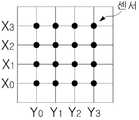
도 1은 상호-커패시턴스 방식 터치 패널을 모식적으로 도시한 평면도이다.1 is a plan view schematically illustrating a mutual-capacitance touch panel.
도 1을 참조하면, 상호-커패시턴스 방식 터치 패널은 일정한 간격으로 배열된 하나 이상의 센서를 포함한다. 각 센서는 하나의 커패시터를 포함하며, 각 센서는 사용자의 터치에 의해 변화하는 커패시턴스를 감지하는 센싱 회로(미도시)에 연결된다.Referring to FIG. 1, a mutual-capacitance touch panel includes one or more sensors arranged at regular intervals. Each sensor includes one capacitor, and each sensor is connected to a sensing circuit (not shown) that senses a capacitance changing by a user's touch.
이하에서는, 상호-커패시턴스 방식 터치 패널의 작동에 대하여 도 2를 참조하여 상세히 설명한다.Hereinafter, the operation of the mutual-capacitance touch panel will be described in detail with reference to FIG. 2.
도 2a는 한 개의 센서와 센싱 회로를 도시한 회로도이며, 도 2b 및 도 2c는 사용자의 터치 입력이 인가되는 경우의 한 개의 센서와 센싱 회로를 도시한 회로도이다.2A is a circuit diagram illustrating one sensor and a sensing circuit, and FIGS. 2B and 2C are circuit diagrams illustrating one sensor and a sensing circuit when a user's touch input is applied.
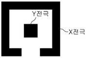
도 2a를 참조하면, 각 센서는 X 전극과 Y 전극으로 구성되는 커패시터를 포함하며, Tx 라인 및 Rx 라인을 통해 센싱 회로와 연결된다. 센싱 회로는 커패시터에 전하를 충전하며, 터치 입력에 의해 변화된 커패시턴스를 검출한다.Referring to FIG. 2A, each sensor includes a capacitor including an X electrode and a Y electrode, and is connected to a sensing circuit through a Tx line and an Rx line. The sensing circuit charges the capacitor and detects the capacitance changed by the touch input.
도 2b 및 도 2c를 참조하면, 사용자의 터치 입력이 인가됨에 따라 X 전극과 Y 전극으로 구성되는 커패시터에 충전된 전하량에 변화가 발생한다. 즉, 도 2c에 도시된 바와 같이, 인체가 커패시터 전극으로 기능하여 터치 입력이 인가되면 Y 전극과 Z 전극으로 구성되는 커패시터가 형성된다. Y 전극과 Z 전극으로 구성되는 커패시터로 인하여 X 전극과 Y 전극으로 구성되는 커패시터에 충전된 전하량이 감소하고, 센싱 회로는 이를 감지하여 사용자 입력을 검출한다.2B and 2C, when a user's touch input is applied, a change occurs in the amount of charge charged in a capacitor composed of an X electrode and a Y electrode. That is, as shown in FIG. 2C, when a human body functions as a capacitor electrode and a touch input is applied, a capacitor including a Y electrode and a Z electrode is formed. Due to the capacitor consisting of the Y electrode and the Z electrode, the amount of charge charged in the capacitor consisting of the X electrode and the Y electrode is reduced, and the sensing circuit detects this to detect a user input.
X 전극과 Y 전극으로 구성되는 커패시터는 SITO(Single Indium Tin Oxide) 방식 또는 DITO(Double Indium Tin Oxide) 방식으로 구현할 수 있다.The capacitor consisting of the X electrode and the Y electrode may be implemented in a single indium tin oxide (SITO) method or a double indium tin oxide (DITO) method.
도 3a 및 도 3b는 각각 SITO 방식 및 DITO 방식을 모식적으로 도시한 단면도이다.3A and 3B are cross-sectional views schematically showing the SITO system and the DITO system, respectively.
도 3a를 참조하면, SITO 방식은 실질적으로 동일한 평면(coplanar) 상에 X 전극과 Y 전극이 형성된다. SITO 방식은 DITO 방식에 비하여 센서의 두께가 얇다는 장점이 있다.Referring to FIG. 3A, in the SITO method, an X electrode and a Y electrode are formed on substantially the same coplanar. SITO method has the advantage that the thickness of the sensor is thinner than the DITO method.
도 3b를 참조하면, DITO 방식은 수직 방향으로 X 전극과 Y 전극이 형성된다. DITO 방식은 SITO 방식에 비하여 노이즈에 강하다는 장점이 있다.Referring to FIG. 3B, in the DITO method, an X electrode and a Y electrode are formed in a vertical direction. The DITO method has an advantage of being more resistant to noise than the SITO method.
X 전극과 Y 전극은 각각 산화 인듐(In2O3)과 산화 주석(SnO2)의 고용체(solid solution)인 ITO(Indium Tin Oxide)로 형성한다. ITO는 투명한 도전성이 있는 산화물로써 터치 패널에 적합한 소재이다. 그러나, RC 상수(RC constant) 값이 커서 터치 패널의 감도를 감소시킨다는 문제점이 있다.The X and Y electrodes are formed of indium tin oxide (ITO), which is a solid solution of indium oxide (In2 O3 ) and tin oxide (SnO2 ), respectively. ITO is a transparent conductive oxide that is suitable for touch panels. However, there is a problem in that the sensitivity of the touch panel is reduced due to a large RC constant value.
ITO 대신에 금속 재료를 사용하면 RC 상수 값을 감소시킬 수 있다. 예를 들어, 도 4에 도시된 X 전극과 Y 전극으로 커패시터를 제조하는 경우 금속 재료의 불투명성으로 인하여 터치 패널의 시인성이 감소한다는 문제점이 있다. 또한, 시인성을 향상시키기 위하여 배선폭을 감소시키는 경우, 사용자 입력을 검출하는데 필요한 커패시턴스를 확보할 수 없다는 문제점이 있다.The use of metallic materials instead of ITO can reduce the RC constant value. For example, when a capacitor is manufactured using the X and Y electrodes illustrated in FIG. 4, there is a problem in that visibility of the touch panel is reduced due to the opacity of the metal material. In addition, when the wiring width is reduced in order to improve visibility, there is a problem in that capacitance required for detecting a user input cannot be secured.
상술한 문제점을 해결하기 위하여, 도 5a에 도시된 메시 패턴을 이용한 도 5b의 X 전극과 Y 전극이 제안되었다.In order to solve the above problem, the X electrode and the Y electrode of FIG. 5B using the mesh pattern shown in FIG. 5A have been proposed.
도 5b의 X 전극과 Y 전극으로 구성되는 커패시터는 도 4의 X 전극과 Y 전극으로 구성되는 커패시터에 비하여 시인성이 우수하다. 그러나, 도 5a에 도시된 메시 패턴은 회절, 굴절, 난반사 및 모아레 현상 등을 발생시켜 시야각(viewing angle)에 따라 시인성이 달라진다는 문제점이 있다.The capacitor composed of the X electrode and the Y electrode of FIG. 5B has better visibility than the capacitor composed of the X electrode and the Y electrode of FIG. 4. However, the mesh pattern illustrated in FIG. 5A generates diffraction, refraction, diffuse reflection, moiré, and the like, so that visibility may vary according to a viewing angle.
본 발명은 벌집형 패턴과 다이아몬드 패턴을 포함하는 메시 패턴을 이용하여 시인성을 향상시킨 벌집형 메시 패턴을 포함하는 정전식 터치 패널용 센서 및 정전식 터치 패널을 제공하는 것을 그 목적으로 한다.An object of the present invention is to provide a sensor for a capacitive touch panel and a capacitive touch panel including a honeycomb mesh pattern having improved visibility by using a mesh pattern including a honeycomb pattern and a diamond pattern.
본 발명에 따른 정전식 터치 패널용 센서는 제1 전극; 및 상기 제1 전극과 커패시터를 형성하는 제2 전극을 포함하되, 상기 제1 전극 및 제2 전극 각각은 상하좌우로 연속되는 하나 이상의 육각 패턴을 포함하는 벌집형 패턴 및 상기 벌집형 패턴에 전기적으로 연결되며, 상하좌우로 연속되는 하나 이상의 사각 패턴을 포함하는 다이아몬드 패턴으로 구성되는 메시 패턴을 포함하되, 상기 하나 이상의 육각 패턴 각각의 중심은 상기 하나 이상의 사각 패턴 각각의 꼭지점과 일치하도록 상기 벌집형 패턴과 상기 다이아몬드 패턴이 오버랩되는 것을 특징으로 한다.The capacitive touch panel sensor according to the present invention includes a first electrode; And a second electrode forming a capacitor with the first electrode, wherein each of the first electrode and the second electrode is electrically connected to the honeycomb pattern and the honeycomb pattern including one or more hexagonal patterns consecutively arranged up, down, left, and right. A mesh pattern comprising a diamond pattern connected to each other, the diamond pattern including one or more square patterns continuous up, down, left, and right, wherein the center of each of the one or more hexagonal patterns coincides with vertices of each of the one or more square patterns. And the diamond pattern overlap.
본 발명에 따른 정전식 터치 패널은 더미 필름; 상기 더미 필름 상부에 구비된 센서층; 및 상기 센서층 상부에 구비된 절연층을 포함하며, 상기 센서층은 제1 전극 및 상기 제1 전극과 커패시터를 형성하는 제2 전극을 포함하는 센서를 구비하며, 상기 제1 전극 및 제2 전극 각각은 상하좌우로 연속되는 하나 이상의 육각 패턴을 포함하는 벌집형 패턴 및 상기 벌집형 패턴에 전기적으로 연결되며, 상하좌우로 연속되는 하나 이상의 사각 패턴을 포함하는 다이아몬드 패턴으로 구성되는 메시 패턴을 포함하되, 상기 하나 이상의 육각 패턴 각각의 중심은 상기 하나 이상의 사각 패턴 각각의 꼭지점과 일치하도록 상기 벌집형 패턴과 상기 다이아몬드 패턴이 오버랩되는 것을 특징으로 한다.Capacitive touch panel according to the present invention is a dummy film; A sensor layer provided on the dummy film; And an insulating layer provided on the sensor layer, wherein the sensor layer includes a first electrode and a second electrode forming a capacitor with the first electrode, wherein the first electrode and the second electrode are provided. Each includes a honeycomb pattern comprising one or more hexagonal patterns continuous up, down, left, and right and a mesh pattern electrically connected to the honeycomb pattern, and a diamond pattern including one or more square patterns continuous up, down, left, and right. The honeycomb pattern and the diamond pattern overlap each other so that a center of each of the one or more hexagonal patterns coincides with a vertex of each of the one or more square patterns.
본 발명에 따른 정전식 터치 패널용 센서는 제1 전극; 및 상기 제1 전극과 커패시터를 형성하는 제2 전극을 포함하되, 상기 제1 전극 및 제2 전극 각각은 상하좌우로 연속되는 단위 패턴을 하나 이상 포함하는 메시 패턴으로 구성되며, 상기 단위 패턴은 제1 변, 제2 변, 제3 변, 상기 제1 변과 대향하는 제4 변, 상기 제2 변과 대향하는 제5 변 및 상기 제3 변과 대향하는 제6 변을 포함하는 육각 금속선 패턴; 및 상기 제1 변과 제4 변을 연결하는 제1 금속선 및 상기 제3 변과 제6 변을 연결하는 제2 금속선을 포함하는 X자 금속선 패턴으로 구성되는 것을 특징으로 한다.The capacitive touch panel sensor according to the present invention includes a first electrode; And a second electrode forming a capacitor with the first electrode, wherein each of the first electrode and the second electrode includes a mesh pattern including one or more unit patterns continuous up, down, left, and right. A hexagonal metal wire pattern including one side, a second side, a third side, a fourth side facing the first side, a fifth side facing the second side, and a sixth side facing the third side; And a first metal line connecting the first side and the fourth side and a second metal line connecting the third side and the sixth side.
상기 제1 전극 및 제2 전극은 동일한 평면상에 위치하는 것이 바람직하다.Preferably, the first electrode and the second electrode are located on the same plane.
상기 하나 이상의 육각 패턴 각각은 금속선으로 구성되는 것이 바람직하다.Each of the one or more hexagonal patterns is preferably composed of a metal wire.
삭제delete
상기 하나 이상의 사각 패턴 각각의 각 변은 물결형 금속선을 포함하는 것이 바람직하다.Each side of each of the one or more square patterns preferably includes a wavy metal line.
삭제delete
상기 금속선의 지름은 2 내지 30㎛인 것이 바람직하며, 5 내지 7㎛인 것이 더욱 바람직하다.It is preferable that the diameter of the said metal wire is 2-30 micrometers, and it is more preferable that it is 5-7 micrometers.
상기 금속선은 은 및 구리 중 어느 하나를 포함하는 것이 바람직하다.It is preferable that the said metal wire contains either silver and copper.
본 발명에 따른 정전식 터치 패널용 센서는 상기 제1 전극 및 제2 전극 사이에 PET 필름을 더 포함하는 것이 바람직하다.Sensor for the capacitive touch panel according to the present invention preferably further comprises a PET film between the first electrode and the second electrode.
상기 더미 필름은 PET 필름 및 반사 방지 필름 중 어느 하나를 포함하는 것이 바람직하다.The dummy film preferably includes any one of a PET film and an antireflection film.
본 발명은 다음과 같은 우수한 효과가 있다.The present invention has the following excellent effects.
본 발명에 따른 센서 및 정전식 터치 패널은 금속선으로 형성된 메시 패턴을 이용하여 전극을 형성하므로 도전성이 우수하고 RC 상수 값이 작다는 장점이 있다.Since the sensor and the capacitive touch panel according to the present invention form an electrode using a mesh pattern formed of a metal wire, the sensor and the capacitive touch panel have excellent conductivity and a small RC constant value.
인쇄 또는 포토리쏘그래피 방식을 이용하여 저저항의 금속으로 본 발명에 따른 메시 패턴을 형성할 수 있어 생산 비용을 낮출 수 있다는 장점이 있다.By using a printing or photolithography method, the mesh pattern according to the present invention can be formed of a low-resistance metal, thereby reducing the production cost.
본 발명에 따른 정전식 터치 패널에 포함된 더미 필름은 광의 난반사, 회절 및 굴절을 감소시켜 우수한 시인성을 제공한다는 장점이 있다.The dummy film included in the capacitive touch panel according to the present invention has an advantage of providing excellent visibility by reducing diffuse reflection, diffraction and refraction of light.
도 1은 상호-커패시턴스 방식 터치 패널을 모식적으로 도시한 평면도.
도 2a 내지 도 2c는 한 개의 센서와 센싱 회로를 도시한 회로도.
도 3a 및 도 3b는 각각 SITO 방식 및 DITO 방식을 모식적으로 도시한 단면도.
도 4는 X 전극 및 Y 전극의 일례를 도시한 평면도.
도 5a 및 도 5b는 각각 종래 기술에 따른 메시 패턴과 이를 적용한 X 전극 및 Y 전극의 일례를 도시한 평면도.
도 6a 내지 도 6b는 본 발명에 따른 메시 패턴을 도시한 평면도.
도 7은 본 발명에 따른 메시 패턴의 단위 패턴을 도시한 평면도.
도 8은 본 발명에 따른 제1 전극 및 제2 전극의 일례를 도시한 단면도.
도 9는 본 발명에 따른 제1 전극 및 제2 전극의 일례를 도시한 평면도.
도 10은 본 발명에 따른 정전식 터치 패널을 도시한 단면도.
도 11은 본 발명에 따른 정전식 터치 패널의 센서층을 도시한 단면도.1 is a plan view schematically showing a mutual-capacitance touch panel;
2A to 2C are circuit diagrams illustrating one sensor and a sensing circuit.
3A and 3B are cross-sectional views schematically showing a SITO system and a DITO system, respectively.
4 is a plan view illustrating one example of an X electrode and a Y electrode;
5A and 5B are plan views illustrating examples of mesh patterns according to the related art and examples of X electrodes and Y electrodes to which the mesh patterns are applied.
6A-6B are plan views illustrating mesh patterns in accordance with the present invention.
7 is a plan view showing a unit pattern of a mesh pattern according to the present invention.
8 is a cross-sectional view showing an example of a first electrode and a second electrode according to the present invention;
9 is a plan view illustrating one example of a first electrode and a second electrode according to the present invention;
10 is a sectional view showing a capacitive touch panel according to the present invention.
11 is a sectional view showing a sensor layer of the capacitive touch panel according to the present invention;
이하에서는, 첨부된 도면을 참조하여 본 발명의 바람직한 실시예를 상세히 설명한다.Hereinafter, with reference to the accompanying drawings will be described in detail a preferred embodiment of the present invention.
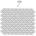
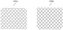
도 6a본 발명에 따른 메시 패턴을 도시한 평면도이며, 도 6b는 발명에 따른 메시 패턴을 벌집형 패턴과 다이아몬드 패턴으로 구분하여 도시한 평면도이다.Figure 6a is a plan view showing a mesh pattern according to the present invention, Figure 6b is a plan view showing the mesh pattern according to the invention divided into a honeycomb pattern and a diamond pattern.
도 6a 및 도 6b를 참조하면, 메시 패턴(600)은 벌집형 패턴(600a)과 다이아몬드 패턴(600b)으로 구성된다. 벌집형 패턴(600a)은 벌집형 패턴(600a)은 금속선으로 구성되며 상하좌우로 연속되는 하나 이상의 육각 패턴을 포함한다. 다이아몬드 패턴(600b)은 벌집형 패턴(600a)에 오버랩되며 벌집형 패턴(600a)에 전기적으로 연결된다. 다이아몬드 패턴(600b)은 금속선으로 구성되며 상하좌우로 연속되는 하나 이상의 사각 패턴을 포함한다. 다이아몬드 패턴(600b)을 구성하는 하나 이상의 사각 패턴 각각의 각 변은 물결형 금속선으로 구성될 수 있다.6A and 6B, the
벌집형 패턴(600a)을 구성하는 하나 이상의 육각 패턴과 다이아몬드 패턴(600b)을 구성하는 금속선은 그 지름이 2 내지 30㎛인 것이 바람직하다. 시인성을 확보하기 위하여 금속선은 그 지름이 5 내지 7㎛인 것이 더욱 바람직하다.At least one hexagonal pattern constituting the
금속선은 은 및 구리 중 어느 하나를 포함할 수 있으며, 표면을 흑화하는 것이 바람직하다.The metal wire may include any one of silver and copper, and it is preferable to blacken the surface.
도 6a에 도시된 바와 같이, 벌집형 패턴(600a)과 다이아몬드 패턴(600b)은 하나 이상의 육각 패턴 각각의 중심과 하나 이상의 사각 패턴 각각의 꼭지점 중 어느 하나와 일치하도록 오버랩된다. 설명의 편의를 위하여, 벌집형 패턴(600a)과 다이아몬드 패턴(600b)을 구분하여 설명하였지만, 벌집형 패턴(600a)과 다이아몬드 패턴(600b)은 일체형으로 구성되는 것이 바람직하다.As shown in FIG. 6A, the
본 발명에 따른 메시 패턴(600)은 인쇄 또는 포토리쏘그래피 방식을 이용하여 형성할 수 있다.The
도 7은 본 발명에 따른 메시 패턴(600)의 단위 패턴을 도시한 평면도이다. 도 6a 및 도 6b에 도시된 바와 같이 메시 패턴(600)을 벌집형 패턴(600a)과 다이아몬드 패턴(600b)으로 구분할 수도 있지만, 설명의 편의를 위하여 도 7에 도시된 바와 같이 메시 패턴(600)을 단위 패턴으로 구분할 수도 있다.7 is a plan view illustrating a unit pattern of the
도 7을 참조하면, 메시 패턴(600)은 상하좌우로 연속되는 단위 패턴(60)을 하나 이상 포함한다. 단위 패턴(50)은 제1 변 내지 제6 변(10-1 내지 10-6)을 포함하는 육각 금속선 패턴과 제1 금속선(20-1) 및 제2 금속선(20-2)을 포함하는 X자 금속선 패턴을 포함한다. 육각 금속선 패턴의 제4 변(10-4)은 제1 변(10-1)과 대향하며, 제3 변(10-3)은 제6 변(10-6)과 대향한다. 제1 금속선(20-1)은 제1 변(10-1)과 제4 변을 연결하며, 제2 금속선(20-2)은 제3 변(10-3)과 제6 변(10-6)을 연결한다.Referring to FIG. 7, the
도 8 및 도 9는 각각 본 발명에 따른 제1 전극 및 제2 전극의 일례를 도시한 단면도 및 평면도이다.8 and 9 are cross-sectional views and plan views showing examples of the first electrode and the second electrode according to the present invention, respectively.
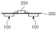
도 8 및 도 9를 참조하면, 제1 전극(100) 및 제2 전극(200)은 각각 메시 패턴(600)을 소정의 형상으로 패터닝하여 형성한다. 도 9에 도시된 제1 전극(100) 및 제2 전극(200)은 본 발명에 따른 메시 패턴(600)으로 형성한 커패시터의 일례이며, 제1 전극(100) 및 제2 전극(200)의 형상이 이에 국한되지는 않는다.8 and 9, the
제1 전극(100) 및 제2 전극(200)은 커패시터, 즉 센서를 형성하며, 본 발명의 터치 패널의 각 노드에 배치된다.The
제1 전극(100) 및 제2 전극(200)은 동일한 평면상(coplanar)에 위치하거나, 절연을 위하여 제1 전극(100) 및 제2 전극(200) 사이에 PET 필름(300)이 삽입될 수도 있다.The
제1 전극; 및
상기 제1 전극과 커패시터를 형성하는 제2 전극
을 포함하되,
상기 제1 전극 및 제2 전극 각각은
상하좌우로 연속되는 하나 이상의 육각 패턴을 포함하는 벌집형 패턴 및 상기 벌집형 패턴에 전기적으로 연결되며, 상하좌우로 연속되는 하나 이상의 사각 패턴을 포함하는 다이아몬드 패턴으로 구성되는 메시 패턴을 포함하되, 상기 하나 이상의 육각 패턴 각각의 중심은 상기 하나 이상의 사각 패턴 각각의 꼭지점과 일치하도록 상기 벌집형 패턴과 상기 다이아몬드 패턴이 오버랩되는 것을 특징으로 하는 정전식 터치 패널용 센서.도 10은 본 발명에 따른 정전식 터치 패널을 도시한 단면도이다.A first electrode; And
A second electrode forming a capacitor with the first electrode
Including,
Each of the first electrode and the second electrode
A honeycomb pattern including one or more hexagonal patterns continuous up, down, left, and right and a mesh pattern electrically connected to the honeycomb pattern, and a diamond pattern including one or more square patterns continuous up, down, left, and right. The center of each of the at least one hexagonal pattern is a sensor for a capacitive touch panel, characterized in that the honeycomb pattern and the diamond pattern overlap so as to coincide with the vertices of each of the at least one square pattern. It is sectional drawing which shows a touch panel.
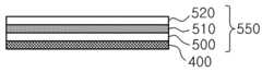
도 10을 참조하면, 본 발명에 따른 정전식 터치 패널(550)은 더미 필름(500), 더미 필름(500) 상부에 구비된 센서층(510) 및 센서층(510) 상부에 구비된 절연층(520)을 포함한다.Referring to FIG. 10, the
더미 필름(500)은 PET 필름(300) 및 반사 방지 필름 중 어느 하나를 포함할수 있으며, 정전식 터치 패널(550)과 디스플레이 패널(400) 사이의 공기층으로 인하여 발생하는 광의 회절, 난반사, 굴절을 감소시켜 사용자의 나안(naked eye)에 센서 패턴이 보이는 현상과 크로스 필터 효과(cross-filter effect)를 감소시키는 기능을 한다.The
도 11은 본 발명에 따른 정전식 터치 패널의 센서층을 도시한 단면도이다.11 is a cross-sectional view illustrating a sensor layer of a capacitive touch panel according to the present invention.
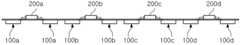
도 11에 도시된 바와 같이, 센서층(510)은 도 6 내지 도 9를 참조하여 설명한 커패시터, 즉 센서를 하나 이상 포함한다. 각 센서는 제1 전극(100a 내지 100d) 및 제2 전극(200a 내지 200d)를 포함한다. 센서는 도 6 내지 도 9를 참조하여 상세히 설명하였으므로 자세한 설명은 생략한다.As shown in FIG. 11, the
100: 제1 전극200: 제2 전극
20-1: 제1 금속선20-2: 제2 금속선
300: PET 필름500: 더미 필름
510: 센서층520: 절연층
550: 정전식 터치 패널600: 메시 패턴
600a: 벌집형 패턴600b: 다이아몬드 패턴
60:단위 패턴100: first electrode 200: second electrode
20-1: First Metal Wire 20-2: Second Metal Wire
300: PET film 500: dummy film
510: sensor layer 520: insulating layer
550
600a:
60: unit pattern
Claims (22)
Translated fromKorean상기 제1 전극과 커패시터를 형성하는 제2 전극
을 포함하되,
상기 제1 전극 및 제2 전극 각각은
상하좌우로 연속되는 하나 이상의 육각 패턴을 포함하는 벌집형 패턴 및 상기 벌집형 패턴에 전기적으로 연결되며, 상하좌우로 연속되는 하나 이상의 사각 패턴을 포함하는 다이아몬드 패턴으로 구성되는 메시 패턴을 포함하되, 상기 하나 이상의 육각 패턴 각각의 중심은 상기 하나 이상의 사각 패턴 각각의 꼭지점과 일치하도록 상기 벌집형 패턴과 상기 다이아몬드 패턴이 오버랩되는 것을 특징으로 하는 정전식 터치 패널용 센서.A first electrode; And
A second electrode forming a capacitor with the first electrode
Including,
Each of the first electrode and the second electrode
A honeycomb pattern including one or more hexagonal patterns continuous up, down, left, and right, and a mesh pattern electrically connected to the honeycomb pattern, and a diamond pattern including one or more square patterns continuous up, down, left, and right. The center of each of the at least one hexagon pattern is a sensor for a capacitive touch panel, characterized in that the honeycomb pattern and the diamond pattern overlap so as to correspond to the vertices of each of the at least one square pattern.
상기 제1 전극 및 제2 전극은 동일한 평면상에 위치하는 것을 특징으로 하는 정전식 터치 패널용 센서.The method of claim 1,
The first electrode and the second electrode is a sensor for a capacitive touch panel, characterized in that located on the same plane.
상기 하나 이상의 육각 패턴 각각은 금속선으로 구성되는 것을 특징으로 하는 정전식 터치 패널용 센서.The method of claim 1,
Each of the at least one hexagonal pattern is a sensor for a capacitive touch panel, characterized in that composed of a metal wire.
상기 하나 이상의 사각 패턴 각각은 금속선으로 구성되는 것을 특징으로 하는 정전식 터치 패널용 센서.The method of claim 1,
Each of the at least one square pattern is a sensor for a capacitive touch panel, characterized in that composed of a metal line.
상기 하나 이상의 사각 패턴 각각의 각 변은 물결형 금속선을 포함하는 것을 특징으로 하는 정전식 터치 패널용 센서.The method of claim 1,
Each side of each of the one or more rectangular patterns, the sensor for a capacitive touch panel, characterized in that it comprises a wavy metal line.
상기 금속선의 지름은 2 내지 30㎛인 것을 특징으로 하는 정전식 터치 패널용 센서.The method according to any one of claims 3 and 4,
The diameter of the metal wire is a sensor for a capacitive touch panel, characterized in that 2 to 30㎛.
상기 금속선의 지름은 5 내지 7㎛인 것을 특징으로 하는 정전식 터치 패널용 센서.The method of claim 7, wherein
The diameter of the metal wire is a sensor for a capacitive touch panel, characterized in that 5 to 7㎛.
상기 금속선은 은 및 구리 중 어느 하나를 포함하는 것을 특징으로 하는 정전식 터치 패널용 센서.The method according to any one of claims 3 and 4,
The metal wire is a sensor for a capacitive touch panel, characterized in that it comprises any one of silver and copper.
상기 제1 전극 및 제2 전극 사이에 PET 필름을 더 포함하는 것을 특징으로 하는 정전식 터치 패널용 센서.The method of claim 1,
Sensor for the capacitive touch panel further comprises a PET film between the first electrode and the second electrode.
상기 더미 필름 상부에 구비된 센서층; 및
상기 센서층 상부에 구비된 절연층
을 포함하며,
상기 센서층은 제1 전극 및 상기 제1 전극과 커패시터를 형성하는 제2 전극을 포함하는 센서를 구비하며, 상기 제1 전극 및 제2 전극 각각은 상하좌우로 연속되는 하나 이상의 육각 패턴을 포함하는 벌집형 패턴 및 상기 벌집형 패턴에 전기적으로 연결되며, 상하좌우로 연속되는 하나 이상의 사각 패턴을 포함하는 다이아몬드 패턴으로 구성되는 메시 패턴을 포함하되, 상기 하나 이상의 육각 패턴 각각의 중심은 상기 하나 이상의 사각 패턴 각각의 꼭지점과 일치하도록 상기 벌집형 패턴과 상기 다이아몬드 패턴이 오버랩되는 것을 특징으로 하는 정전식 터치 패널.Dummy film;
A sensor layer provided on the dummy film; And
Insulation layer provided on the sensor layer
Including;
The sensor layer includes a sensor including a first electrode and a second electrode forming a capacitor with the first electrode, each of the first electrode and the second electrode including one or more hexagonal patterns that are continuous in a vertical direction. And a mesh pattern composed of a honeycomb pattern and a diamond pattern electrically connected to the honeycomb pattern, the diamond pattern including one or more square patterns continuous up, down, left, and right, and the center of each of the one or more hexagonal patterns is one or more squares. And the honeycomb pattern and the diamond pattern overlap each other to correspond to vertices of the patterns.
상기 제1 전극 및 제2 전극은 동일한 평면상에 위치하는 것을 특징으로 하는 정전식 터치 패널.The method of claim 11,
And the first electrode and the second electrode are on the same plane.
상기 하나 이상의 육각 패턴 각각은 금속선으로 구성되는 것을 특징으로 하는 정전식 터치 패널.The method of claim 11,
The at least one hexagonal pattern each of the capacitive touch panel, characterized in that composed of a metal wire.
상기 하나 이상의 사각 패턴 각각은 금속선으로 구성되는 것을 특징으로 하는 정전식 터치 패널.The method of claim 11,
Each of the at least one rectangular pattern is a capacitive touch panel, characterized in that composed of a metal line.
상기 하나 이상의 사각 패턴 각각의 각 변은 물결형 금속선을 포함하는 것을 특징으로 하는 정전식 터치 패널.The method of claim 11,
Each side of each of the one or more rectangular patterns, each capacitive touch panel comprising a wavy metal line.
상기 금속선의 지름은 2 내지 30㎛인 것을 특징으로 하는 정전식 터치 패널.The method according to any one of claims 11 and 14,
The diameter of the metal wire is a capacitive touch panel, characterized in that 2 to 30㎛.
상기 금속선의 지름은 5 내지 7㎛인 것을 특징으로 하는 정전식 터치 패널.The method of claim 17,
The metal wire has a diameter of 5 to 7㎛ capacitive touch panel, characterized in that.
상기 금속선은 은 및 구리 중 어느 하나를 포함하는 것을 특징으로 하는 정전식 터치 패널.The method according to any one of claims 13 and 14,
The metal wire includes any one of silver and copper.
상기 제1 전극 및 제2 전극 사이에 PET 필름을 더 포함하는 것을 특징으로 하는 정전식 터치 패널.The method of claim 11,
Capacitive touch panel further comprises a PET film between the first electrode and the second electrode.
상기 더미 필름은 PET 필름 및 반사 방지 필름 중 어느 하나를 포함하는 것을 특징으로 하는 정전식 터치 패널.The method of claim 11,
The dummy film includes any one of a PET film and an antireflection film.
상기 제1 전극과 커패시터를 형성하는 제2 전극
을 포함하되,
상기 제1 전극 및 제2 전극 각각은 상하좌우로 연속되는 단위 패턴을 하나 이상 포함하는 메시 패턴으로 구성되며, 상기 단위 패턴은 제1 변, 제2 변, 제3 변, 상기 제1 변과 대향하는 제4 변, 상기 제2 변과 대향하는 제5 변 및 상기 제3 변과 대향하는 제6 변을 포함하는 육각 금속선 패턴; 및 상기 제1 변과 제4 변을 연결하는 제1 금속선 및 상기 제3 변과 제6 변을 연결하는 제2 금속선을 포함하는 X자 금속선 패턴으로 구성되는 것을 특징으로 하는 정전식 터치 패널용 센서.A first electrode; And
A second electrode forming a capacitor with the first electrode
Including,
Each of the first electrode and the second electrode includes a mesh pattern including one or more unit patterns continuous up, down, left, and right, and the unit pattern faces the first side, the second side, the third side, and the first side. A hexagonal metal wire pattern including a fourth side, a fifth side facing the second side, and a sixth side facing the third side; And an X-shaped metal wire pattern including a first metal wire connecting the first side and the fourth side and a second metal wire connecting the third side and the sixth side. .
Priority Applications (2)
| Application Number | Priority Date | Filing Date | Title |
|---|---|---|---|
| KR1020110049604AKR101111564B1 (en) | 2011-05-25 | 2011-05-25 | Sensors and capacitive touch panels for capacitive touch panels with honeycomb mesh patterns |
| US13/206,782US20120299865A1 (en) | 2011-05-25 | 2011-08-10 | Sensor for Capacitive Touch Panel Including Mesh Pattern and Capacitive Touch Panel Including the Same |
Applications Claiming Priority (1)
| Application Number | Priority Date | Filing Date | Title |
|---|---|---|---|
| KR1020110049604AKR101111564B1 (en) | 2011-05-25 | 2011-05-25 | Sensors and capacitive touch panels for capacitive touch panels with honeycomb mesh patterns |
Publications (1)
| Publication Number | Publication Date |
|---|---|
| KR101111564B1true KR101111564B1 (en) | 2012-02-24 |
Family
ID=45840126
Family Applications (1)
| Application Number | Title | Priority Date | Filing Date |
|---|---|---|---|
| KR1020110049604AExpired - Fee RelatedKR101111564B1 (en) | 2011-05-25 | 2011-05-25 | Sensors and capacitive touch panels for capacitive touch panels with honeycomb mesh patterns |
Country Status (1)
| Country | Link |
|---|---|
| KR (1) | KR101111564B1 (en) |
Cited By (2)
| Publication number | Priority date | Publication date | Assignee | Title |
|---|---|---|---|---|
| KR20150017380A (en)* | 2012-07-11 | 2015-02-16 | 다이니폰 인사츠 가부시키가이샤 | Touch panel sensor, touch panel device, and display device |
| KR20160034020A (en) | 2014-09-19 | 2016-03-29 | 동우 화인켐 주식회사 | Touch Sensor Panel and Method for Fabricating the same |
Citations (4)
| Publication number | Priority date | Publication date | Assignee | Title |
|---|---|---|---|---|
| US20090084613A1 (en)* | 2007-09-28 | 2009-04-02 | Au Optronics Corporation | Capacitive Touch Panel with Low Coupling Capacitance and Display Device Using the Capacitive Touch Panel |
| JP2010176571A (en)* | 2009-01-30 | 2010-08-12 | Dmc:Kk | Touch panel |
| US20110007030A1 (en)* | 2009-07-09 | 2011-01-13 | Michael Mo | Ultrathin mutual capacitance touch screen and combined ultrathin touch screen |
| JP2011059771A (en)* | 2009-09-07 | 2011-03-24 | Hitachi Chem Co Ltd | Mesh-shaped conductive pattern and base material with conductor layer pattern and touch panel member |
- 2011
- 2011-05-25KRKR1020110049604Apatent/KR101111564B1/ennot_activeExpired - Fee Related
Patent Citations (4)
| Publication number | Priority date | Publication date | Assignee | Title |
|---|---|---|---|---|
| US20090084613A1 (en)* | 2007-09-28 | 2009-04-02 | Au Optronics Corporation | Capacitive Touch Panel with Low Coupling Capacitance and Display Device Using the Capacitive Touch Panel |
| JP2010176571A (en)* | 2009-01-30 | 2010-08-12 | Dmc:Kk | Touch panel |
| US20110007030A1 (en)* | 2009-07-09 | 2011-01-13 | Michael Mo | Ultrathin mutual capacitance touch screen and combined ultrathin touch screen |
| JP2011059771A (en)* | 2009-09-07 | 2011-03-24 | Hitachi Chem Co Ltd | Mesh-shaped conductive pattern and base material with conductor layer pattern and touch panel member |
Cited By (11)
| Publication number | Priority date | Publication date | Assignee | Title |
|---|---|---|---|---|
| KR20150017380A (en)* | 2012-07-11 | 2015-02-16 | 다이니폰 인사츠 가부시키가이샤 | Touch panel sensor, touch panel device, and display device |
| KR20170057466A (en)* | 2012-07-11 | 2017-05-24 | 다이니폰 인사츠 가부시키가이샤 | Touch panel sensor, touch panel device, and display device |
| KR102006089B1 (en)* | 2012-07-11 | 2019-07-31 | 다이니폰 인사츠 가부시키가이샤 | Touch panel sensor, touch panel device, and display device |
| KR102008047B1 (en)* | 2012-07-11 | 2019-08-06 | 다이니폰 인사츠 가부시키가이샤 | Touch panel sensor, touch panel device, and display device |
| US10416826B2 (en) | 2012-07-11 | 2019-09-17 | Dai Nippon Printing Co., Ltd. | Touch panel sensor, touch panel device and display device |
| US10521063B2 (en) | 2012-07-11 | 2019-12-31 | Dai Nippon Printing Co., Ltd. | Touch panel sensor, touch panel device and display device |
| US10901563B2 (en) | 2012-07-11 | 2021-01-26 | Dai Nippon Printing Co., Ltd | Touch panel sensor, touch panel device and display device |
| KR20160034020A (en) | 2014-09-19 | 2016-03-29 | 동우 화인켐 주식회사 | Touch Sensor Panel and Method for Fabricating the same |
| US10303274B2 (en) | 2014-09-19 | 2019-05-28 | Dongwoo Fine-Chem Co., Ltd. | Touch sensor panel and method formanufacturing same |
| US10386946B2 (en) | 2014-09-19 | 2019-08-20 | Dongwoo Fine-Chem Co., Ltd. | Touch sensor panel and method for fabricating the same |
| US10401995B2 (en) | 2014-09-19 | 2019-09-03 | Dongwoo Fine-Chem Co., Ltd. | Touch sensor panel and method for fabricating the same |
Similar Documents
| Publication | Publication Date | Title |
|---|---|---|
| US20120299865A1 (en) | Sensor for Capacitive Touch Panel Including Mesh Pattern and Capacitive Touch Panel Including the Same | |
| TWI585659B (en) | Capacitive touch panel and method for fabricating touch panel reducing visibility of its metal conductor | |
| KR101395195B1 (en) | Touch screen with mesh electrode pattern | |
| US10254904B2 (en) | Conductive sheet, capacitive touch panel, and display device | |
| TWI522867B (en) | In-cell organic light emitting diode touch panel | |
| CN102902425B (en) | Capacitance type touch-control panel structure and manufacture method | |
| US9007332B2 (en) | Position sensing panel | |
| KR101128669B1 (en) | Touch panel sensor including low resistant line pattern | |
| US20120229414A1 (en) | Position sensing panel | |
| TWI628565B (en) | Conductive sheet, capacitive touch panel and display device | |
| US20120098782A1 (en) | Touch panel sensor | |
| JP3182680U (en) | Touch panel | |
| JP2011530113A (en) | Touch sensing device with composite electrode | |
| US10359890B2 (en) | Touch screen, touch panel, and display apparatus | |
| KR101470075B1 (en) | Touch panel | |
| CN103576968A (en) | Touch substrate, display panel and patterned shading layer | |
| KR100954898B1 (en) | Touch panel sensor | |
| KR20140002947U (en) | Touch electrode device | |
| KR102254179B1 (en) | Touch display apparatus | |
| KR101111565B1 (en) | Sensors and capacitive touch panels for capacitive touch panels with honeycomb mesh patterns | |
| KR101111564B1 (en) | Sensors and capacitive touch panels for capacitive touch panels with honeycomb mesh patterns | |
| CN111699461A (en) | Transparent electrode member, laminated transparent electrode member, and capacitance sensor | |
| CN202661991U (en) | Touch-control panel and electronic equipment | |
| CN205644489U (en) | Touch -sensitive screen of embedded forced induction function | |
| TW201439833A (en) | Touch panel |
Legal Events
| Date | Code | Title | Description |
|---|---|---|---|
| A201 | Request for examination | ||
| PA0109 | Patent application | St.27 status event code:A-0-1-A10-A12-nap-PA0109 | |
| PA0201 | Request for examination | St.27 status event code:A-1-2-D10-D11-exm-PA0201 | |
| P11-X000 | Amendment of application requested | St.27 status event code:A-2-2-P10-P11-nap-X000 | |
| P13-X000 | Application amended | St.27 status event code:A-2-2-P10-P13-nap-X000 | |
| A302 | Request for accelerated examination | ||
| PA0302 | Request for accelerated examination | St.27 status event code:A-1-2-D10-D17-exm-PA0302 St.27 status event code:A-1-2-D10-D16-exm-PA0302 | |
| D13-X000 | Search requested | St.27 status event code:A-1-2-D10-D13-srh-X000 | |
| D14-X000 | Search report completed | St.27 status event code:A-1-2-D10-D14-srh-X000 | |
| PE0902 | Notice of grounds for rejection | St.27 status event code:A-1-2-D10-D21-exm-PE0902 | |
| E13-X000 | Pre-grant limitation requested | St.27 status event code:A-2-3-E10-E13-lim-X000 | |
| P11-X000 | Amendment of application requested | St.27 status event code:A-2-2-P10-P11-nap-X000 | |
| P13-X000 | Application amended | St.27 status event code:A-2-2-P10-P13-nap-X000 | |
| E701 | Decision to grant or registration of patent right | ||
| PE0701 | Decision of registration | St.27 status event code:A-1-2-D10-D22-exm-PE0701 | |
| GRNT | Written decision to grant | ||
| PR0701 | Registration of establishment | St.27 status event code:A-2-4-F10-F11-exm-PR0701 | |
| PR1002 | Payment of registration fee | St.27 status event code:A-2-2-U10-U11-oth-PR1002 Fee payment year number:1 | |
| PG1601 | Publication of registration | St.27 status event code:A-4-4-Q10-Q13-nap-PG1601 | |
| PN2301 | Change of applicant | St.27 status event code:A-5-5-R10-R11-asn-PN2301 | |
| PN2301 | Change of applicant | St.27 status event code:A-5-5-R10-R14-asn-PN2301 | |
| P14-X000 | Amendment of ip right document requested | St.27 status event code:A-5-5-P10-P14-nap-X000 | |
| P16-X000 | Ip right document amended | St.27 status event code:A-5-5-P10-P16-nap-X000 | |
| Q16-X000 | A copy of ip right certificate issued | St.27 status event code:A-4-4-Q10-Q16-nap-X000 | |
| FPAY | Annual fee payment | Payment date:20150126 Year of fee payment:4 | |
| PR1001 | Payment of annual fee | St.27 status event code:A-4-4-U10-U11-oth-PR1001 Fee payment year number:4 | |
| FPAY | Annual fee payment | Payment date:20160126 Year of fee payment:5 | |
| PR1001 | Payment of annual fee | St.27 status event code:A-4-4-U10-U11-oth-PR1001 Fee payment year number:5 | |
| LAPS | Lapse due to unpaid annual fee | ||
| PC1903 | Unpaid annual fee | St.27 status event code:A-4-4-U10-U13-oth-PC1903 Not in force date:20170127 Payment event data comment text:Termination Category : DEFAULT_OF_REGISTRATION_FEE | |
| PC1903 | Unpaid annual fee | St.27 status event code:N-4-6-H10-H13-oth-PC1903 Ip right cessation event data comment text:Termination Category : DEFAULT_OF_REGISTRATION_FEE Not in force date:20170127 | |
| P22-X000 | Classification modified | St.27 status event code:A-4-4-P10-P22-nap-X000 |