KR101111439B1 - Control Method for Three-phase Z-Source Inverter - Google Patents
Control Method for Three-phase Z-Source InverterDownload PDFInfo
- Publication number
- KR101111439B1 KR101111439B1KR1020100050408AKR20100050408AKR101111439B1KR 101111439 B1KR101111439 B1KR 101111439B1KR 1020100050408 AKR1020100050408 AKR 1020100050408AKR 20100050408 AKR20100050408 AKR 20100050408AKR 101111439 B1KR101111439 B1KR 101111439B1
- Authority
- KR
- South Korea
- Prior art keywords
- voltage
- modulation index
- actual
- vector
- command
- Prior art date
- Legal status (The legal status is an assumption and is not a legal conclusion. Google has not performed a legal analysis and makes no representation as to the accuracy of the status listed.)
- Expired - Fee Related
Links
Images


Landscapes
- Inverter Devices (AREA)
Abstract
Translated fromKorean
Description
Translated fromKorean본 발명은 전압형 전압형 3상 Z소스 인버터의 제어방법에 관한 것으로, 특히 간소화된 방법으로 출력전압의 안정화를 구현할 수 있는 3상 Z전압원 인버터의 제어방법에 관한 것이다.
The present invention relates to a control method of a voltage type voltage three-phase Z source inverter, and more particularly, to a control method of a three-phase Z voltage source inverter capable of implementing stabilization of an output voltage in a simplified manner.
전압형 3상 Z소스 인버터는 인덕터와 커패시터로 구성된 Z 임피던스 망(Z-Source Network)를 종전의 부스트(boost) 장치를 대신하므로 구성면에서 single stage 구성의 DC-AC 전력변환시스템과 유사하여 출력전압의 손실이 낮다.Voltage-type three-phase Z source inverters replace Z-source networks consisting of inductors and capacitors in place of conventional boost devices, so the output voltage is similar to that of single stage DC-AC power conversion system. The loss of is low.
이러한 전압형 3상 Z소스 인버터를 제어하는 일반적인 방법은 동일 암의 두 스위치의 단락 시간을 이용하여 boost율을 결정하기 때문에 데드시간이 불필요하며, 인버터 동작 중 영 전압 구간에 단락 구간을 구성하므로 손실이 낮고 종전의 시스템 보다 높은 출력을 기대할 수 있다. 따라서 스위치 소자의 손실 가능성이 낮고 구성이 간단하여 신뢰성 및 출력효율이 높다.The general method of controlling such a voltage-type three-phase Z source inverter uses the short time of the two switches of the same arm to determine the boost rate, thereby eliminating the dead time, and forming a short section in the zero voltage section during the inverter operation. You can expect this lower and higher output than the previous system. Therefore, the loss of the switch element is low and the configuration is simple, so the reliability and the output efficiency are high.
하지만 종전의 전압형 3상 Z 소스 인버터의 전압 안정화를 위한 제어방법은 DQ 변환을 통해 3가지 상 전압을 직류전압 값으로 변형하여 지령전압과 비교하는 방식을 기본으로 사용하였다. 이러한 방식은 3가지 상 전압을 검출하기 위한 장치 및 DQ 변환과 추가적인 복잡한 알고리즘을 요구한다.
However, the control method for voltage stabilization of the conventional voltage type three-phase Z source inverter used a method of converting three phase voltages into DC voltage values through DQ conversion and comparing them with the reference voltage. This approach requires a device for detecting three phase voltages and DQ conversion and additional complex algorithms.
본 발명은 상기와 같은 종래 기술의 문제점 및 기술 개발의 필요성을 해결하기 위해 안출된 것으로, 간소화 된 알고리즘으로 출력 전압을 안정화시킬 수 있는 전압형 3상 Z소스 인버터의 제어방법을 제공하는 데에 그 목적이 있다.
The present invention has been made to solve the problems of the prior art and the necessity of the technical development as described above, to provide a control method of a voltage type three-phase Z source inverter that can stabilize the output voltage with a simplified algorithm There is a purpose.
상기의 목적을 달성하기 위해서 본 발명에 의한 전압형 3상 Z소스 인버터 제어방법은 전압이득을 검출하는 제 1 단계; 전압이득 관계식을 바탕으로 변조지수를 결정하는 제 2 단계; 추종 변조지수 결정하는 제 3 단계; 및 추종 변조지수를 이용하여 인버터의 스위치부를 제어하는 제 4 단계;를 포함한다.In order to achieve the above object, a voltage-type three-phase Z source inverter control method according to the present invention includes a first step of detecting a voltage gain; Determining a modulation index based on a voltage gain relationship; A third step of determining a tracking modulation index; And a fourth step of controlling the switch unit of the inverter using the following modulation index.
제 1 단계는 지령 지령출력전압 제어를 위한 커패시터 인가전압을 결정하여, 커패시터 인가전압과 입력전압의 관계식을 이용하여 지령 전압이득을 검출하는 단계; 및 실제 커패시터 인가전압과 입력전압의 관계식을 이용하여 실제 전압이득을 검출하는 단계;를 포함할 수 있다.The first step includes determining a capacitor applied voltage for controlling the command command output voltage, and detecting a command voltage gain using a relationship between the capacitor applied voltage and the input voltage; And detecting an actual voltage gain using a relationship between an actual capacitor applied voltage and an input voltage.
제 2 단계는 암 단락 지수로 정의되는 전압이득에서, 암 단락 지수를 변조지수 관계식으로 대체함으로써 지령 변조지수 및 실제 변조지수를 전압이득 관계식으로 표현하는 것일 수 있다.The second step may be to express the command modulation index and the actual modulation index in a voltage gain relationship by substituting the modulation index relation in the voltage gain defined by the dark short index.
제 3 단계는 지령 변조지수(Mref) 및 실제 변조지수(Mactual)를 비교하여 다음과 같은 관계식으로 추종 변조지수(Mfollow)를 결정하는 것일 수 있다.The third step may be to compare the command modulation index (Mref ) and the actual modulation index (Mactual ) to determine the following modulation index (Mfollow ) by the following relationship.
[수학식][Equation]
Mfollow= ( Mref- Mactual) + MactualMfollow = (Mref Mactual ) + Mactual
제 4 단계는 공간벡터 변조방식의 출력전압 정의와 두 유효벡터 인가시간 정의를 이용하여, 다음의 수학식과 같은 유효벡터(VN,VN+1)의 인가시간(TN, TN+1)을 정의함으로써 스위치부를 제어하는 것일 수 있다.In the fourth step, using the output voltage definition of the space vector modulation method and the definition of the two effective vector application times, the application time (TN , TN+1 ) of the effective vector (VN , VN+1 ) is expressed by the following equation. May be to control the switch unit.
[수학식][Equation]


그리고 제 4 단계에서 스위치부를 제어하는 것은 암 단락 벡터(VD)의 인가시간(TD)을 다음과 같은 수학식으로 제어하는 것일 수 있다.And to control the switch unit in the fourth step may be to control the application time (TD) of the short-arm vector (VD) by the following mathematical expression:
[수학식][Equation]

또한, 제 4 단계에서 스위치부를 제어하는 것은 영 전압 벡터(VZ)의 인가시간(TZ)을 다음과 같은 수학식을 이용하여 제어하는 것일 수 있다.In addition, controlling the switch unit in the fourth step may be to control the application time (TZ ) of the zero voltage vector (VZ ) using the following equation.
[수학식][Equation]

상술한 바와 같이 본 발명에 따르면, 지령 변조지수와 실제 변조지수의 비교를 통해서 변조지수의 최적화 된 추종범위가 결정되며 추종 변조지수의 범위가 미달 또는 초과되는 현상이 발생하지 않는다. 따라서 추종 변조지수로 추종이 매우 빠르고 제어방법이 간소화된다.
As described above, according to the present invention, an optimized tracking range of the modulation index is determined by comparing the command modulation index with the actual modulation index, and a phenomenon in which the range of the following modulation index is less than or exceeded does not occur. Therefore, following the modulation index is very fast and the control method is simplified.
도 1은 본 발명에 의한 인버터 제어방법을 나타내는 시스템 블록도.
도 2 내지 도 6은 본 발명에 의한 인버터 제어를 위한 각각의 시스템의 연산 알고리즘을 나타내는 도면들.
도 7 및 도 8은 공간벡터 변조 방식을 설명하기 위한 도면들
도 9 내지 도 12는 본 발명에 의한 인버터 제어의 시뮬레이션 결과를 나타내는 도면들.1 is a system block diagram showing an inverter control method according to the present invention.
2 to 6 are diagrams showing the calculation algorithm of each system for inverter control according to the present invention.
7 and 8 are diagrams for explaining a space vector modulation scheme.
9 to 12 are diagrams showing simulation results of inverter control according to the present invention.
본 발명에서 사용되는 용어는 가능한 현재 널리 사용되는 일반적인 용어를 선택하였으나, 특정한 경우는 출원인이 임의로 선정한 용어도 있는데 이 경우에는 단순한 용어의 명칭이 아닌 발명의 상세한 설명 부분에 기재되거나 사용된 의미를 고려하여 그 의미가 파악되어야 할 것이다.The terms used in the present invention were selected as general terms as widely used as possible, but in some cases, the terms arbitrarily selected by the applicant are included. In this case, the meanings described or used in the detailed description of the present invention are considered, rather than simply the names of the terms. The meaning should be grasped.
이하, 본 발명에 따른 실시예를 첨부된 도면을 참조하여 구체적으로 설명하기로 한다.Hereinafter, embodiments of the present invention will be described in detail with reference to the accompanying drawings.
도 1은 본 발명에 의한 전압형 3상 Z소스 인버터의 제어방법을 나타내기 위한 시스템의 블록도이다.1 is a block diagram of a system for illustrating a control method of a voltage type three-phase Z source inverter according to the present invention.
도 1을 참조하면, 본 발명에 의한 전압형 3상 Z소스 인버터의 제어방법은 먼저 지령 전압이득(Gref)과 실제 전압이득(Gactual)을 검출한다.Referring to FIG. 1, the control method of the voltage type three-phase Z source inverter according to the present invention first detects the command voltage gain Gref and the actual voltage gain Gactual .
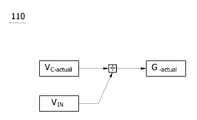
이를 위해서 전압이득 검출부(100)의 실제 전압이득(Gactual) 검출부(110) 및 지령 전압이득(Gref) 검출부(120)는 각각 도 2 및 도 3에서 표현한 것과 같은 알고리즘을 수행한다. 즉, 전압이득(G)은 다음의 [수학식 1]과 같이 커패시터 인가전압(Vc)과 입력전압(VIN)의 관계식으로 표현할 수 있다.The actual voltage gain of the

그리고 공간벡터 변조방식(SVM)을 사용하는 Z 전압원 인버터의 출력전압(VOUT)은 다음의 [수학식 2]와 같다.In addition, the output voltage VOUT of the Z voltage source inverter using the space vector modulation method (SVM) is expressed by

부하에 따라 항상 일정한 지령출력을 유지하기 위한 지령 전압이득(Gref)과 실제 전압이득(Gactual)은 입력전압(VIN)과 커패시터 인가전압(Vc-actual)의 연산을 통해 알 수 있다. 다시 말해서 지령 전압이득(Gref)은 상술한 [수학식 2]를 이용하여 지령출력 전압 제어를 위한 커패시터 인가전압을 결정하고 [수학식 1]을 이용하여 결정할 수 있다. 동일한 방법으로 실제 전압이득(Gactual)은 입력전압(VIN)과 실제 커패시터 인가전압(Vc-actual)으로 결정할 수 있다.The command voltage gain (Gref ) and the actual voltage gain (Gactual ) to maintain a constant command output at all times depending on the load can be obtained by calculating the input voltage (VIN ) and the capacitor applied voltage (Vc-actual ). . In other words, the command voltage gain Gref may be determined by using
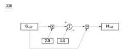
변조지수 변환부(200)는 전압이득 검출부(100)에 의해서 상술한 방법으로 결정된 지령 전압이득(Gref)과 실제 전압이득(Gactual)을 이용하여 지령 변조지수(Mref)와 현재 동작 중인 실제 변조지수(Mactual)를 유도할 수 있다.The
도 4 및 도 5는 이처럼 변조지수 유도를 위한 실제 변조지수 변환부(210) 및 지령 변조지수 변환부(220)의 연산 알고리즘을 나타내는 도면들이다. 이러한 연산을 위해서 변조지수(M) 및 전압이득(G)의 관계가 G=(1-D)/(1-2D)=M?D 인 것을 이용한다. 이때 B는 부스트 팩터(boost factor)로써, 입력 직류전압이 Z-Impedance Network 이후에 인버터 측에 걸리는 전압의 부스트(Boost) 정도를 나타낸다. 또한 암 단락 지수(D)는 동일 암의 두 스위치의 단락 비(shoot through duty ratio)를 의미한다.4 and 5 are diagrams illustrating an operation algorithm of the actual
그리고, 상술한 변조지수(M) 및 전압이득(G)의 관계식에서 암 단락 지수는 '1-M'과 같으므로 변조지수(M)는 다음과 같은 [수학식 3]으로 표현할 수 있다.In addition, since the dark short index is equal to '1-M' in the relational expression of the modulation index M and the voltage gain G, the modulation index M may be expressed as

즉, [수학식 3]을 이용하여 지령 변조지수(Mref)와 현재 동작 중인 실제 변조지수(Mactual)를 지령 전압이득(Gref)과 실제 전압이득(Gactual)의 관계식으로 표현할 수 있다.In other words, using
변조지수 추종부(300)는 도 6과 같은 연산 알고리즘으로 지령 변조지수(Mref)와 실제 변조지수(Mactual)의 비교를 통해서 출력전압 안정화를 위한 추종 변조지수(Mfollow)를 결정한다. 이처럼 변조지수 추종부(300)가 변조지수를 추종시키는 방법은 다음의 [수학식 4]와 같다.The

즉, 지령 변조지수(Mref)와 실제 변조지수(Mactual)가 지령 변조지수(Mref)와 동일해지기 위한 추종 범위값(에러값)을 경정하고 실제 변조지수(Mactual)에 추종 범위값을 연산하여 전압 안정화를 위한 추종 변조지수(Mfollow)를 결정한다.That is, the following range (error value) is determined to make the command modulation index (Mref ) and the actual modulation index (Mactual ) equal to the command modulation index (Mref ), and the range following the actual modulation index (Mactual ). The value is calculated to determine thefollow modulation index (Mfollow ) for voltage stabilization.
동작중인 Z 전압원 인버터의 실제 출력전압이 지령 출력전압 보다 낮은 경우에는 [실제 변조지수(Mactual)>지령 변조지수(Mref)]의 관계식이 성립한다. 따라서 에러값은 (-)값을 가지게 되고, 에러값과 실제 변조지수의 연산을 통해서 추종 변조지수는 지령 변조지수와 동일해진다. 반대로 지령 출력전압이 실제 출력전압 보다 낮은 경우에는 [실제 변조지수(Mactual)<지령 변조지수(Mref)]의 관계를 갖게 되므로 에러값은 (+)값이므로 실제 변조지수와의 연산을 통해서 추종 변조지수(Mfollow)와 동일한 값을 가지게 된다. 이러한 방법으로 종전에 사용되었던 출력전압의 DQ 변환, PI 제어를 필요치 않고 간단한 연산을 통해서 변조지수의 추종범위를 최적으로 결정하여 즉시 추종하는 것이 가능하다.When the actual output voltage of the Z voltage source inverter in operation is lower than the command output voltage, the relationship between [actual modulation index (Mactual )> command modulation index (Mref )] holds. Therefore, the error value has a negative value, and the following modulation index becomes the same as the command modulation index through the calculation of the error value and the actual modulation index. On the contrary, when the command output voltage is lower than the actual output voltage, it has a relationship between [actual modulation index (Mactual ) <command modulation index (Mref )]. Therefore, the error value is a positive value. It has the same value as the following modulation index (Mfollow ). In this way, it is possible to immediately follow the optimal determination of the tracking range of the modulation index through simple calculations without the need for DQ conversion and PI control of the output voltage.
상술한 방법으로 획득된 추종 변조지수를 이용하여 인버터를 제어하는 방법을 살펴보면 다음과 같다.Looking at the method of controlling the inverter using the following modulation index obtained by the above-described method as follows.
도 7은 공간벡터 변조방식의 벡터 공간도이다.7 is a vector space diagram of a space vector modulation method.
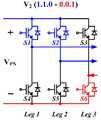
도 7을 참조하면, 육각형의 벡터 공간의 각 모서리에 표시된 6개의 벡터(Vec1 내지 Vec6)는 지령 벡터(Reference Vec)가 회전하는 동안 스위치부(500)의 온-오프(on-off)신호를 의미한다.Referring to FIG. 7, the six vectors Vec1 to Vec6 displayed at each corner of the hexagonal vector space receive the on-off signal of the
도 8a 내지 도 8f는 도 1에 도시된 스위치부(500)를 나타내는 도면으로서 지령벡터에 따른 제 1 내지 제 6 스위치(S1,S2,S3,S4,S5,S6) 간의 신호 흐름을 나타내는 도면들이다. 이때 괄호 안은 제 1 내지 제 6 스위치(S1,S2,S3,S4,S5,S6)들의 온-오프 신호를 나타낸다.8A to 8F are diagrams illustrating the
공간벡터를 이용한 인버터의 제어방법은 육각형의 벡터공간에서 회전하는 지령 벡터(Reference Vec)를 이용한다. 지령 벡터(Reference Vec)가 360° 1회전 시 출력파형은 완전한 정현파가 출력된다. 그리고 출력파형인 정현파의 완전한 형태로 출력되기 위해서는 지령 벡터(Reference Vec)는 제 1 서클(circle.1)의 범위 내에서 회전하여야 한다. 이때 지령 벡터(Reference Vec)의 크기는 출력 정현파의 크기에 비례하고, 회전속도는 출력 정현파의 주파수에 해당한다.The control method of the inverter using the space vector uses a reference vector (Reference Vec) rotating in a hexagonal vector space. When the reference vector (Reference Vec) is rotated 360 °, the output waveform is a full sine wave. In order to output a sinusoidal waveform that is an output waveform, the reference vector Reference Vec must rotate within the range of the first circle. At this time, the magnitude of the reference vector (Reference Vec) is proportional to the magnitude of the output sinusoid, and the rotation speed corresponds to the frequency of the output sinusoid.
도 9는 지령 벡터에 회전에 의한 출력 정현파를 나타내는 도면이다. 도 8에서와 같이 지령 벡터는 각 유효벡터와 겹쳐서 60°씩 회전하지 않고 전체 360°구간을 1°씩 회전한다. 이에 따라 실제 출력 정현파의 파형은 각 섹터로 나눌 수 있다. 위의 과정을 계속해서 반복하면 출력전압은 정현파를 지속적으로 출력한다. 이때 출력되는 정현파는 다음의 [수학식 5]와 같이 표현할 수 있다.9 is a diagram illustrating an output sinusoidal wave by rotation in a command vector. As shown in FIG. 8, the command vector rotates the entire 360 ° section by 1 ° without overlapping with each effective vector by 60 °. Accordingly, the waveform of the actual output sinusoid can be divided into sectors. If the above process is repeated repeatedly, the output voltage continuously outputs the sine wave. At this time, the output sine wave can be expressed as


여기에서 SN은 각 섹터의 번호(1~6)를 의미한다. 그리고 α는 지령 벡터와 Vec1 간의 각도를 나타낸다. 그리고 지령벡터에 인접한 두 유효벡터(Vn,Vn+1)의 인가시간(Tn,Tn+1)의 관계식을 유도하기 위해서, 일반적인 공간벡터 변조방식의 출력전압의 관계식과 두 유효벡터 인가시간 관계식을 살펴보면 다음과 같다.Here, SN means the
일반적인 공간벡터 변조방식의 출력전압은 다음의 [수학식 6]와 같이 표현할 수 있다The output voltage of the general spatial vector modulation method can be expressed as

그리고, 두 유효벡터 인가시간 정의를 표현하는 아래의 [수학식 7]과 같다.In addition, Equation 7 below is used to express two valid vector application time definitions.


위의 [수학식 6] 및 [수학식 7]을 이용하여 두 유효벡터 인가시간을 정의하면 다음의 [수학식 8]과 같다.Using the above [Equation 6] and [Equation 7] to define the two effective vector application time is shown in the following [Equation 8].


또한 지령벡터와 암 단락 벡터(VD)가 최대 내접원 안에서 일정한 규칙으로 존재하기 때문에 암 단락 벡터(VD)의 인가시간(TD) 역시 변조지수를 이용하여 다음의 [수학식 9]과 같이 유도할 수 있다.In addition, since the command vector and the arm short vector (VD ) exist as a regular rule in the maximum inscribed circle, the application time (TD ) of the arm short vector (VD ) is also expressed using the modulation index as shown in [Equation 9]. Can be induced.

따라서 남은 영 전압 벡터(Vz)의 인가시간(Tz)은 암 단락 벡터(VD)와 지령 벡터 영역을 제외한 크기를 갖게 되므로 [수학식 10]과 같이 표현할 수 있다.Therefore, since the application time Tz of the remaining zero voltage vector Vz has a size excluding the dark short vector VD and the command vector region, it can be expressed as shown in [Equation 10].

도 10은 상술한 내용을 바탕으로 하여 제 1 내지 제 6 스위치()를 제어하기 위한 신호들의 타임 차트(time-chart)를 나타내는 도면이다.FIG. 10 is a diagram illustrating a time chart of signals for controlling the first to sixth switches A based on the above description.
도 10을 참조하면, 변조 지수에 의해 암 단락 인가시간(TD) 및다른 벡터의 인가 시간이 결정된다. 그리고 각 인가시간의 합은 TS로 동일하다. 타임 차트를 바탕으로 교류출력의 위상각 마다 각 인가시간은 변화하고, 제 1 내지 제 6 스위치는 6개의 유효벡터(V1 내지V6) 및영 벡터(VZ)에 해당하는 6개의 스위칭 패턴에 의해 동작한다.Referring to FIG. 10, the dark short application time TD and the application time of another vector are determined by the modulation index. And the sum of each application time is equal to TS. Based on the time chart, each application time is changed for each phase angle of the AC output, and the first to sixth switches are applied to six switching patterns corresponding to six valid vectors V1 to V6 and zero vectors VZ. It works by
이와 같이 본 발명은 인버터용 공간 벡터 변조방식에서 각 벡터의 크기 및 인가시간을 변조지수만으로 결정할 수 있다. 또한 동일한 변조지수에서는 항상 일정한 암 단락 인가시간(TD)을 유지하는 것이 가능할 뿐 아니라 각 벡터의 영역이 다른 벡터 영역을 절대 포함하지 않는다. 또한 변조 영역으로 벗어나는 현상이 발생하지 않으므로 출력전압의 왜곡 현상이 발생하지 않는다.As described above, according to the present invention, the size and the application time of each vector in the space vector modulation method for the inverter can be determined using only the modulation index. In addition, it is not only possible to maintain a constant dark short application time TD at the same modulation index, but also each region of the vector never includes another vector region. In addition, since the phenomenon of deviation to the modulation region does not occur, the distortion of the output voltage does not occur.
다음의 [표 1]은 도 11 내지 도 14에 도시된 PSIM 시뮬레이션에 사용한 파라미터를 나타내고 있다.Table 1 below shows parameters used for the PSIM simulation shown in FIGS. 11 to 14.
(156.0V)110 VRMS
(156.0V)
시뮬레이션에서 0.01s이전 시간 동안 변조지수는 1.0으로 유지하고 이후 시간부터는 제안한 알고리즘을 적용하였다. 0.1s를 기준으로 입력전압(VIN)이 100.0V에서 150.0V로 50% 상승 되거나 100V에서 50V로 50%로 감소되고 0.2s를 기준으로 하여 부하가 30.0Ω에서 10.0Ω으로 감소되는 상황을 가정하여 시뮬레이션 하였다.In the simulation, the modulation index was maintained at 1.0 for the time before 0.01 s, and the proposed algorithm was applied after that. Suppose that the input voltage (VIN ) increases by 50% from 100.0V to 150.0V based on 0.1s, or decreases by 50% from 100V to 50V, and the load decreases from 30.0Ω to 10.0Ω based on 0.2s. Simulated by
입력전압(VIN)과 커패시터 인가전압(VC)을 이용하여 ZSI의 출력 교류전압을 제어하는 제안된 알고리즘의 블록선도를 그림 10에 나타내었다. 본 연구에서 제안된 변조지수 추종방법 및 공간벡터 변조방법은 일실시예로 PSIM의 DLL(dynamic library link) 블록을 사용하여 구현될 수 있고, 시뮬레이션 역시 이를 기반으로 수행되었다.The block diagram of the proposed algorithm for controlling the output AC voltage of ZSI using the input voltage (VIN ) and capacitor applied voltage (VC ) is shown in Figure 10. The modulation index tracking method and the space vector modulation method proposed in this study can be implemented using the DLL (dynamic library link) block of PSIM as an example, and the simulation is performed based on this.
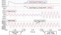
도 11은 부하가 30.0ohm인 조건 하에서 VIN이 0.1s부터 100.0V에서 50.0V로 변화될 때, 그리고 0.2s부터 부하가 10.0ohm으로 감소되는 경우에 대한 실제 전압이득(Gactual)과 지령 전압이득(Gref) 및 실제 변조지수(Mactual)의 추종범위, 전압 안정화를 위한 추종 변조지수(Mfollow)를 차례로 나타내었다. 입력전압이 상승되는 순간 변조지수는 0.6140에서 0.6921로 즉시 변화한 것을 알 수 있다.11 is a time a change in VIN from the 0.1s 100.0V to 50.0V under the condition that the load 30.0ohm, and the actual voltage gain for the case that the load is reduced to 10.0ohm from 0.2s (Gactual) and the reference voltage The tracking range of the gainGref , the actual modulation index Mactual , and the tracking modulation index Mfollow for voltage stabilization are shown in this order. As soon as the input voltage rises, the modulation index immediately changes from 0.6140 to 0.6921.
도 12는 입력전압(VIN)과 커패시터 인가전압(VC-actual) 및 변조지수(Mfollow)변화, 한 상(Phase)에 대한 출력파형을 나타내었으며 출력전압이 110VRMS(156V)로 일정하게 유지됨을 알 수 있다. 입력전압(VIN) 이 증가하는 경우 순간 Z-임피던스 망을 구성하는 커패시터 인가전압(VC-actual)과 교류 출력전압은 거의 변화 없이 동일함을 알 수 있다. 그리고, 부하가 감소한 경우 약간의 과도상태를 거친 후 출력전압은 110VRMS(156V)을 그대로 유지하는 것을 알 수 있다.12 shows the input voltage (VIN ), the capacitor applied voltage (VC-actual ), the modulation index (Mfollow ) change, the output waveform for one phase, and the output voltage is constant at 110VRMS (156V). It can be seen that it is maintained. It can be seen that when the input voltage (VIN ) increases, the capacitor applied voltage (VC-actual ) constituting the instantaneous Z-impedance network and the AC output voltage are almost identical. In addition, when the load decreases, after a slight transient state, the output voltage is maintained at 110VRMS (156V).
도 13은 부하가 30.0ohm인 조건 하에서 입력전압(VIN)이 0.1s부터 100.0V에서 50.0V로 변화될 때 그리고 0.2s부터 부하가 10.0ohm으로 감소되는 경우의 실제 전압이득(Gactual)과 지령 전압이득(Gref) 및 실제 변조지수(Mactual)의 추종범위, 전압 안정화를 위한 추종변조지수(Mfollow)를 차례로 나타내었다. 입력전압이 감소되는 순간 변조지수는 0.6140에서 0.55로 즉시 변화한 것을 알 수 있다.FIG. 13 shows the actual voltage gain (Gactual ) when the input voltage (VIN ) changes from 0.1s to 100.0V to 50.0V under the condition that the load is 30.0 ohm and when the load is reduced to 10.0 ohm from 0.2s. The following shows the following ranges of the command voltage gain (Gref ), the actual modulation index (Mactual ), and the follow modulation index (Mfollow ) for voltage stabilization. As soon as the input voltage decreases, the modulation index immediately changes from 0.6140 to 0.55.
도 14는 입력전압(VIN)과 커패시터 인가전압(VC-actual) 및 변조지수(Mfollow), 한 상(Phase)에 대한 출력파형을 나타내었으며 110VRMS(156V)로 안정화 된 출력파형을 볼 수 있다. 입력전압(VIN)이 감소하는 경우 역시 Z-임피던스 망을 구성하는 커패시터 인가전압(VC-actual)과 출력전압은 거의 변동이 없으며 부하가 감소한 경우에는 짧은 시간 동안(약 반주기)의 과도상태를 거친 후 출력전압이 110VRMS(156V)으로 안정화된 것을 알 수 있다.14 shows the output waveforms for the input voltage (VIN ), the capacitor applied voltage (VC-actual ), the modulation index (Mfollow ), and one phase, and shows the output waveform stabilized at 110VRMS (156V). can see. When the input voltage (VIN ) decreases, the capacitor applied voltage (VC-actual ) and the output voltage constituting the Z-impedance network are almost unchanged. After passing through, it can be seen that the output voltage has stabilized to 110VRMS (156V).
상술한 바와 같이 본 발명에 의한 전압형 3상 Z소스 인버터 제어방법은 지령 변조지수와 실제 변조지수의 간단한 연산을 통해 추종하는 방법을 이용하기 때문에 출력전압의 DQ변환이나 PI 제어 등을 사용하지 않는다. 즉 간단히 지령 변조지수와 실제 변조지수의 비교를 통해서 변조지수의 최적화 된 추종범위가 결정되며 추종 변조지수의 범위가 미달 또는 초과되는 현상이 발생하지 않는다. 따라서 추종 변조지수로 추종이 매우 빠르고 다른 제어방법을 요구하지 않는다.As described above, the voltage-type three-phase Z source inverter control method according to the present invention does not use the output voltage DQ conversion or PI control because it uses a method of following a simple calculation of the command modulation index and the actual modulation index. . That is, the optimized tracking range of the modulation index is determined by simply comparing the command modulation index with the actual modulation index, and there is no phenomenon that the range of the following modulation index is less than or exceeded. Therefore, the following modulation index is very fast and does not require any other control method.
그리고 Z 전압원 인버터의 출력전압에 대한 추종된 변조지수가 우선 결정되므로 공간벡터 변조방식을 적용하기 위해서 출력전압에 대한 부스트 팩터(B), 전압이득, 암 단락지수 등을 따로 고려할 필요없이 변조지수만을 이용하여 각 벡터 및 인가시간을 제어할 수 있다. 또한 변조지수와 암 단락 지수가 고정된 값 안에서 변화되는 특성상 각 벡터는 다른 벡터의 영역을 포함하는 경우가 발생하지 않고 과변조 영역으로 벗어나는 현상도 발생하지 않아서 신뢰성이 높다.Since the following modulation index is determined first for the output voltage of the Z voltage source inverter, only the modulation index is required without considering the boost factor (B), the voltage gain, and the dark short circuit index for the output voltage. Each vector and the application time can be controlled. In addition, because the modulation index and the dark short index are changed within a fixed value, each vector does not include the region of another vector and does not occur to the overmodulation region.
본 발명은 이상에서 살펴본 바와 같이 바람직한 실시 예를 들어 설명하였으나, 상기한 실시 예에 한정되지 아니하며 본 발명의 요지를 벗어나지 않는 범위 내에서 당해 발명이 속하는 기술분야에서 통상의 지식을 가진 자에 의해 다양한 변경과 수정이 가능할 것이다.As described above, the present invention has been described with reference to preferred embodiments, but is not limited to the above-described embodiments, and various modifications may be made by those skilled in the art without departing from the gist of the present invention. Changes and corrections will be possible.
Claims (7)
Translated fromKorean상기 전압이득 관계식을 바탕으로 변조지수를 결정하는 제 2 단계;
추종 변조지수 결정하는 제 3 단계; 및
상기 추종 변조지수를 이용하여 인버터의 스위치부를 제어하는 제 4 단계;를 포함하고,
상기 제 3 단계는
지령 변조지수(Mref) 및 실제 변조지수(Mactual)의 비교를 함으로써, 다음과 같은 관계식으로 상기 추종 변조지수(Mfollow)를 결정하는 것을 특징으로 하는 전압형 3상 Z소스 인버터 제어방법.
[수학식]
Mfollow= ( Mref- Mactual) + Mactual
A first step of detecting a voltage gain using a relation between an input voltage and a capacitor;
Determining a modulation index based on the voltage gain relationship;
A third step of determining a tracking modulation index; And
And a fourth step of controlling the switch unit of the inverter by using the following modulation index.
The third step is
And comparing the reference modulation index (Mref ) and the actual modulation index (Mactual ) to determine the following modulation index (Mfollow ) according to the following relationship.
[Equation]
Mfollow = (Mref -Mactual ) + Mactual
상기 제 1 단계는
지령 지령출력전압 제어를 위한 커패시터 인가전압을 결정하여, 상기 커패시터 인가전압과 입력전압의 관계식을 이용하여 지령 전압이득을 검출하는 단계; 및
실제 커패시터 인가전압과 상기 입력전압의 관계식을 이용하여 실제 전압이득을 검출하는 단계;를 포함하는 것을 특징으로 하는 전압형 3상 Z소스 인버터 제어방법.
The method of claim 1,
The first step is
Determining a capacitor applied voltage for command command output voltage control and detecting a command voltage gain using a relational expression between the capacitor applied voltage and the input voltage; And
And detecting an actual voltage gain by using a relationship between an actual capacitor applied voltage and the input voltage.
상기 제 2 단계는
암 단락 지수로 정의되는 상기 전압이득에서, 상기 암 단락 지수를 상기 변조지수 관계식으로 대체함으로써 지령 변조지수 및 실제 변조지수를 상기 전압이득 관계식으로 표현하는 것을 특징으로 전압형 3상 Z소스 인버터 제어방법.
The method of claim 1,
The second step is
In the voltage gain defined by the dark short index, the command modulation index and the actual modulation index are represented by the voltage gain relation by replacing the dark short index with the modulation index relation. .
상기 제 4 단계에서 상기 스위치부를 제어하는 하는 것은 공간벡터 변조방식의 출력전압 정의와 두 유효벡터 인가시간 정의를 이용하여, 다음의 수학식과 같이 정의되는 유효벡터 인가시간(VN,VN+1)을 이용하는 것을 특징으로 하는 전압형 3상 Z소스 인버터 제어방법.
[수학식]


The method of claim 1,
The controlling of the switch unit in the fourth step uses an output voltage definition of the spatial vector modulation method and two effective vector application time definitions, and an effective vector application time (VN , VN + 1) is defined as follows. Voltage-type three-phase Z source inverter control method characterized in that using.
[Equation]
상기 제 4 단계에서 상기 스위치부를 제어하는 것은 다음과 같은 수학식으로 정의되는 암 단락 벡터(VD)의 인가시간(TD)을 이용하는 것을 특징으로 하는 전압형 3상 Z소스 인버터 제어방법.
[수학식]

The method of claim 5, wherein
The controlling of the switch unit in the fourth step is a voltage-type three-phase Z source inverter control method, characterized in that using the application time (TD ) of the dark short vector (VD ) defined by the following equation.
[Equation]
상기 제 4 단계에서 상기 스위치부를 제어하는 것은 다음과 같은 수학식으로 정의되는 영 전압 벡터(VZ)의 인가시간(TZ)을 이용하는 것을 특징으로 하는 전압형 3상 Z소스 인버터 제어방법.
[수학식]

The method according to claim 6,
The controlling of the switch unit in the fourth step is a voltage type three-phase Z source inverter control method, characterized in that using the applied time (TZ) of the zero voltage vector (VZ) defined by the following equation.
[Equation]
Priority Applications (1)
| Application Number | Priority Date | Filing Date | Title |
|---|---|---|---|
| KR1020100050408AKR101111439B1 (en) | 2010-05-28 | 2010-05-28 | Control Method for Three-phase Z-Source Inverter |
Applications Claiming Priority (1)
| Application Number | Priority Date | Filing Date | Title |
|---|---|---|---|
| KR1020100050408AKR101111439B1 (en) | 2010-05-28 | 2010-05-28 | Control Method for Three-phase Z-Source Inverter |
Publications (2)
| Publication Number | Publication Date |
|---|---|
| KR20110130869A KR20110130869A (en) | 2011-12-06 |
| KR101111439B1true KR101111439B1 (en) | 2012-04-06 |
Family
ID=45499497
Family Applications (1)
| Application Number | Title | Priority Date | Filing Date |
|---|---|---|---|
| KR1020100050408AExpired - Fee RelatedKR101111439B1 (en) | 2010-05-28 | 2010-05-28 | Control Method for Three-phase Z-Source Inverter |
Country Status (1)
| Country | Link |
|---|---|
| KR (1) | KR101111439B1 (en) |
Cited By (1)
| Publication number | Priority date | Publication date | Assignee | Title |
|---|---|---|---|---|
| CN103973152A (en)* | 2014-04-04 | 2014-08-06 | 深圳职业技术学院 | Pulse width modulation control method and pulse width modulation control device |
Families Citing this family (1)
| Publication number | Priority date | Publication date | Assignee | Title |
|---|---|---|---|---|
| CN116191844B (en)* | 2023-02-22 | 2024-08-09 | 中国矿业大学 | A Z-source inverter control method and device with optimized switching loss and common-mode voltage reduction |
Citations (3)
| Publication number | Priority date | Publication date | Assignee | Title |
|---|---|---|---|---|
| US7130205B2 (en) | 2002-06-12 | 2006-10-31 | Michigan State University | Impedance source power converter |
| US20090001923A1 (en) | 2007-06-29 | 2009-01-01 | Gm Global Technology Operations, Inc. | Systems and methods for operating z-source inverter inductors in a continuous current mode |
| US7768228B2 (en) | 2007-09-12 | 2010-08-03 | Gm Global Technology Operations, Inc. | Method and system for converting DC power to AC power |
- 2010
- 2010-05-28KRKR1020100050408Apatent/KR101111439B1/ennot_activeExpired - Fee Related
Patent Citations (3)
| Publication number | Priority date | Publication date | Assignee | Title |
|---|---|---|---|---|
| US7130205B2 (en) | 2002-06-12 | 2006-10-31 | Michigan State University | Impedance source power converter |
| US20090001923A1 (en) | 2007-06-29 | 2009-01-01 | Gm Global Technology Operations, Inc. | Systems and methods for operating z-source inverter inductors in a continuous current mode |
| US7768228B2 (en) | 2007-09-12 | 2010-08-03 | Gm Global Technology Operations, Inc. | Method and system for converting DC power to AC power |
Non-Patent Citations (2)
| Title |
|---|
| 전력전자 추계학술대회 논문집(제목: 이득 및 변조지수 제어에 의한 Z-소스 인버터의 출력전압 제어), 논문발표 2009년 11월* |
| 전력전자 추계학술대회 논문집(제목: 이득 및 변조지수 제어에 의한 Z-소스 인버터의 출력전압 제어), 논문발표 2009년 11월* |
Cited By (2)
| Publication number | Priority date | Publication date | Assignee | Title |
|---|---|---|---|---|
| CN103973152A (en)* | 2014-04-04 | 2014-08-06 | 深圳职业技术学院 | Pulse width modulation control method and pulse width modulation control device |
| CN103973152B (en)* | 2014-04-04 | 2016-10-05 | 深圳职业技术学院 | A kind of pulse width modulation control method and device |
Also Published As
| Publication number | Publication date |
|---|---|
| KR20110130869A (en) | 2011-12-06 |
Similar Documents
| Publication | Publication Date | Title |
|---|---|---|
| Townsend et al. | Phase-shifted carrier modulation techniques for cascaded H-bridge multilevel converters | |
| CN110557039A (en) | inverter control device | |
| CN109510496B (en) | Neutral point voltage balance control method and system for NPC three-level inverter without electrolytic capacitor | |
| Jin et al. | Reduction of dc-link capacitance for three-phase three-wire shunt active power filters | |
| Dey et al. | Synchronous reference frame based control technique for shunt hybrid active power filter under non-ideal voltage | |
| CN104601028A (en) | Neutral-point voltage control system and method for parameter on-line tuning | |
| JP4703251B2 (en) | Operation method of power supply device and power supply device | |
| Chatterjee | A bus clamping PWM-based improved control of grid tied PV inverter with LCL filter under varying grid frequency condition | |
| Karmiris et al. | A multifunction control scheme for current harmonic elimination and voltage sag mitigation using a three phase three level flying capacitor inverter | |
| KR101111439B1 (en) | Control Method for Three-phase Z-Source Inverter | |
| Nannam et al. | A detailed modeling and comparative analysis of hysteresis current controlled Vienna rectifier and space vector pulse width modulated Vienna rectifier in mitigating the harmonic distortion on the input mains | |
| Rajagopal et al. | Shunt active filter based on 7-level cascaded multilevel inverter for harmonic and reactive power compensation | |
| JP6437807B2 (en) | Control circuit for controlling inverter circuit and inverter device provided with the control circuit | |
| Gopalan | A comparative study of control techniques for three phase PWM rectifier | |
| CN106385197A (en) | Output voltage control method for inverter independent operation and controller | |
| JP2016063687A (en) | Power converter | |
| CN111446877B (en) | Control method and system based on two-phase three-bridge-arm inverter circuit | |
| Lin et al. | Analysis and implementation of a three-level active filter with a reduced number of power semiconductors | |
| Zhou et al. | A carrier-based DPWM method with variable clamped interval for NPC three-level inverter | |
| Komurcugil | Hysteresis current-control strategy for single-phase half-bridge shunt active power filters | |
| Shah et al. | Generalized current control scheme for unity power factor two-level and three-level bi-directional front-end power converters: An approach for multi-level front-end converters | |
| Cheng et al. | A modified one cycle control of Vienna rectifier for neutral point voltage balancing control based on cycle-by-cycle correction | |
| Tekwani et al. | Implementation of sector change detection schemes for current error space phasor hysteresis controller based Shunt Active Power Filters | |
| Hsu et al. | Grid Voltage Balancing Strategy Based on Per-Phase-Controlled Inverters | |
| Tao et al. | Virtual-flux-based predictive direct power control of three-phase AC/DC converters |
Legal Events
| Date | Code | Title | Description |
|---|---|---|---|
| A201 | Request for examination | ||
| PA0109 | Patent application | St.27 status event code:A-0-1-A10-A12-nap-PA0109 | |
| PA0201 | Request for examination | St.27 status event code:A-1-2-D10-D11-exm-PA0201 | |
| E902 | Notification of reason for refusal | ||
| PE0902 | Notice of grounds for rejection | St.27 status event code:A-1-2-D10-D21-exm-PE0902 | |
| PG1501 | Laying open of application | St.27 status event code:A-1-1-Q10-Q12-nap-PG1501 | |
| E13-X000 | Pre-grant limitation requested | St.27 status event code:A-2-3-E10-E13-lim-X000 | |
| P11-X000 | Amendment of application requested | St.27 status event code:A-2-2-P10-P11-nap-X000 | |
| P13-X000 | Application amended | St.27 status event code:A-2-2-P10-P13-nap-X000 | |
| E90F | Notification of reason for final refusal | ||
| PE0902 | Notice of grounds for rejection | St.27 status event code:A-1-2-D10-D21-exm-PE0902 | |
| P11-X000 | Amendment of application requested | St.27 status event code:A-2-2-P10-P11-nap-X000 | |
| P13-X000 | Application amended | St.27 status event code:A-2-2-P10-P13-nap-X000 | |
| E701 | Decision to grant or registration of patent right | ||
| PE0701 | Decision of registration | St.27 status event code:A-1-2-D10-D22-exm-PE0701 | |
| GRNT | Written decision to grant | ||
| PR0701 | Registration of establishment | St.27 status event code:A-2-4-F10-F11-exm-PR0701 | |
| PR1002 | Payment of registration fee | St.27 status event code:A-2-2-U10-U11-oth-PR1002 Fee payment year number:1 | |
| PG1601 | Publication of registration | St.27 status event code:A-4-4-Q10-Q13-nap-PG1601 | |
| R18-X000 | Changes to party contact information recorded | St.27 status event code:A-5-5-R10-R18-oth-X000 | |
| PN2301 | Change of applicant | St.27 status event code:A-5-5-R10-R13-asn-PN2301 St.27 status event code:A-5-5-R10-R11-asn-PN2301 | |
| FPAY | Annual fee payment | Payment date:20141230 Year of fee payment:4 | |
| PR1001 | Payment of annual fee | St.27 status event code:A-4-4-U10-U11-oth-PR1001 Fee payment year number:4 | |
| R18-X000 | Changes to party contact information recorded | St.27 status event code:A-5-5-R10-R18-oth-X000 | |
| FPAY | Annual fee payment | Payment date:20151218 Year of fee payment:5 | |
| PR1001 | Payment of annual fee | St.27 status event code:A-4-4-U10-U11-oth-PR1001 Fee payment year number:5 | |
| R18-X000 | Changes to party contact information recorded | St.27 status event code:A-5-5-R10-R18-oth-X000 | |
| FPAY | Annual fee payment | Payment date:20161228 Year of fee payment:6 | |
| PR1001 | Payment of annual fee | St.27 status event code:A-4-4-U10-U11-oth-PR1001 Fee payment year number:6 | |
| P22-X000 | Classification modified | St.27 status event code:A-4-4-P10-P22-nap-X000 | |
| LAPS | Lapse due to unpaid annual fee | ||
| PC1903 | Unpaid annual fee | St.27 status event code:A-4-4-U10-U13-oth-PC1903 Not in force date:20180127 Payment event data comment text:Termination Category : DEFAULT_OF_REGISTRATION_FEE | |
| R18-X000 | Changes to party contact information recorded | St.27 status event code:A-5-5-R10-R18-oth-X000 | |
| PC1903 | Unpaid annual fee | St.27 status event code:N-4-6-H10-H13-oth-PC1903 Ip right cessation event data comment text:Termination Category : DEFAULT_OF_REGISTRATION_FEE Not in force date:20180127 |