KR101111063B1 - Apparatus for joining of substrate - Google Patents
Apparatus for joining of substrateDownload PDFInfo
- Publication number
- KR101111063B1 KR101111063B1KR1020080138517AKR20080138517AKR101111063B1KR 101111063 B1KR101111063 B1KR 101111063B1KR 1020080138517 AKR1020080138517 AKR 1020080138517AKR 20080138517 AKR20080138517 AKR 20080138517AKR 101111063 B1KR101111063 B1KR 101111063B1
- Authority
- KR
- South Korea
- Prior art keywords
- chamber
- upper chamber
- substrate
- support
- screw
- Prior art date
- Legal status (The legal status is an assumption and is not a legal conclusion. Google has not performed a legal analysis and makes no representation as to the accuracy of the status listed.)
- Expired - Fee Related
Links
Images


Classifications
- G—PHYSICS
- G02—OPTICS
- G02F—OPTICAL DEVICES OR ARRANGEMENTS FOR THE CONTROL OF LIGHT BY MODIFICATION OF THE OPTICAL PROPERTIES OF THE MEDIA OF THE ELEMENTS INVOLVED THEREIN; NON-LINEAR OPTICS; FREQUENCY-CHANGING OF LIGHT; OPTICAL LOGIC ELEMENTS; OPTICAL ANALOGUE/DIGITAL CONVERTERS
- G02F1/00—Devices or arrangements for the control of the intensity, colour, phase, polarisation or direction of light arriving from an independent light source, e.g. switching, gating or modulating; Non-linear optics
- G02F1/01—Devices or arrangements for the control of the intensity, colour, phase, polarisation or direction of light arriving from an independent light source, e.g. switching, gating or modulating; Non-linear optics for the control of the intensity, phase, polarisation or colour
- G02F1/13—Devices or arrangements for the control of the intensity, colour, phase, polarisation or direction of light arriving from an independent light source, e.g. switching, gating or modulating; Non-linear optics for the control of the intensity, phase, polarisation or colour based on liquid crystals, e.g. single liquid crystal display cells
- G02F1/1303—Apparatus specially adapted to the manufacture of LCDs
- G—PHYSICS
- G02—OPTICS
- G02F—OPTICAL DEVICES OR ARRANGEMENTS FOR THE CONTROL OF LIGHT BY MODIFICATION OF THE OPTICAL PROPERTIES OF THE MEDIA OF THE ELEMENTS INVOLVED THEREIN; NON-LINEAR OPTICS; FREQUENCY-CHANGING OF LIGHT; OPTICAL LOGIC ELEMENTS; OPTICAL ANALOGUE/DIGITAL CONVERTERS
- G02F1/00—Devices or arrangements for the control of the intensity, colour, phase, polarisation or direction of light arriving from an independent light source, e.g. switching, gating or modulating; Non-linear optics
- G02F1/01—Devices or arrangements for the control of the intensity, colour, phase, polarisation or direction of light arriving from an independent light source, e.g. switching, gating or modulating; Non-linear optics for the control of the intensity, phase, polarisation or colour
- G02F1/13—Devices or arrangements for the control of the intensity, colour, phase, polarisation or direction of light arriving from an independent light source, e.g. switching, gating or modulating; Non-linear optics for the control of the intensity, phase, polarisation or colour based on liquid crystals, e.g. single liquid crystal display cells
- G02F1/133—Constructional arrangements; Operation of liquid crystal cells; Circuit arrangements
- G02F1/1333—Constructional arrangements; Manufacturing methods
- G02F1/1339—Gaskets; Spacers; Sealing of cells
- G—PHYSICS
- G02—OPTICS
- G02F—OPTICAL DEVICES OR ARRANGEMENTS FOR THE CONTROL OF LIGHT BY MODIFICATION OF THE OPTICAL PROPERTIES OF THE MEDIA OF THE ELEMENTS INVOLVED THEREIN; NON-LINEAR OPTICS; FREQUENCY-CHANGING OF LIGHT; OPTICAL LOGIC ELEMENTS; OPTICAL ANALOGUE/DIGITAL CONVERTERS
- G02F1/00—Devices or arrangements for the control of the intensity, colour, phase, polarisation or direction of light arriving from an independent light source, e.g. switching, gating or modulating; Non-linear optics
- G02F1/01—Devices or arrangements for the control of the intensity, colour, phase, polarisation or direction of light arriving from an independent light source, e.g. switching, gating or modulating; Non-linear optics for the control of the intensity, phase, polarisation or colour
- G02F1/13—Devices or arrangements for the control of the intensity, colour, phase, polarisation or direction of light arriving from an independent light source, e.g. switching, gating or modulating; Non-linear optics for the control of the intensity, phase, polarisation or colour based on liquid crystals, e.g. single liquid crystal display cells
- G02F1/133—Constructional arrangements; Operation of liquid crystal cells; Circuit arrangements
- G02F1/1333—Constructional arrangements; Manufacturing methods
- G02F1/133354—Arrangements for aligning or assembling substrates
- G—PHYSICS
- G02—OPTICS
- G02F—OPTICAL DEVICES OR ARRANGEMENTS FOR THE CONTROL OF LIGHT BY MODIFICATION OF THE OPTICAL PROPERTIES OF THE MEDIA OF THE ELEMENTS INVOLVED THEREIN; NON-LINEAR OPTICS; FREQUENCY-CHANGING OF LIGHT; OPTICAL LOGIC ELEMENTS; OPTICAL ANALOGUE/DIGITAL CONVERTERS
- G02F2202/00—Materials and properties
- G02F2202/28—Adhesive materials or arrangements
Landscapes
- Physics & Mathematics (AREA)
- Nonlinear Science (AREA)
- Chemical & Material Sciences (AREA)
- Crystallography & Structural Chemistry (AREA)
- General Physics & Mathematics (AREA)
- Optics & Photonics (AREA)
- Engineering & Computer Science (AREA)
- Manufacturing & Machinery (AREA)
- Mathematical Physics (AREA)
- Container, Conveyance, Adherence, Positioning, Of Wafer (AREA)
Abstract
Translated fromKoreanDescription
Translated fromKorean본 발명은 기판합착장치에 관한 것으로, 더욱 상세하게는 두 기판을 합착하는 기판합착장치에 관한 것이다.The present invention relates to a substrate bonding apparatus, and more particularly to a substrate bonding apparatus for bonding two substrates.
정보화 사회가 발전함에 따라 디스플레이 장치에 대한 요구도 다양한 형태로 증가되어 왔다. 이에 근래에는 LCD(Lipuid Crystal Display Device), PDP(Plasma Display Panel), ELD(Electro Luminescent Display), VFD(Vacuum Fluorescent Display)등 여러 가지 평판 디스플레이 장치가 연구되어 왔고 그 일부는 이미 실생활에 널리 사용되고 있다.As the information society has developed, the demand for display devices has increased in various forms. Recently, various flat panel display devices such as LCD (Lipuid Crystal Display Device), PDP (Plasma Display Panel), ELD (Electro Luminescent Display), VFD (Vacuum Fluorescent Display) have been studied and some of them are widely used in real life. .
그 중 LCD의 경우에는 CRT(Cathode Ray Tube)에 비하여 화질이 우수하고 경량, 박형, 저소비 전력의 특징에 따른 장점으로 인하여 이동형 화상 표시장치의 용도로 많이 사용되고 있다.Among them, LCDs are being used for mobile image display devices because of their excellent image quality compared to CRT (Cathode Ray Tube) and the advantages of light weight, thinness, and low power consumption.
이러한 LCD는 전극이 형성되어 있는 TFT(Thin Film Transistor) 기판과 형광체가 도포된 CF(Color filter) 기판 사이에 액정(Liquid Crystal)을 주입하여 형성된다. 두 기판 사이에는 소정 간격으로 두 기판 사이의 간격을 유지하기 위한 간격재(Spacer)가 배치되며, 두 기판의 외주면에는 액정 물질을 누출을 막기 위한 밀봉 재(Sealer)가 배치된다.The LCD is formed by injecting a liquid crystal between a TFT (Thin Film Transistor) substrate on which an electrode is formed and a CF (Color filter) substrate coated with phosphors. Spacers are disposed between the two substrates to maintain a gap between the two substrates at predetermined intervals, and a sealer is disposed on the outer circumferential surfaces of the two substrates to prevent leakage of the liquid crystal material.
따라서 LCD를 제조함에 있어서, TFT기판 및 CF 기판을 각각 제조한 후에 양 기판을 합착하고 그 사이의 공간에 액정 물질을 주입하는 공정이 필수적으로 필요하며 이중 기판을 합착시키는 공정은 LCD의 품질을 결정하는 중요한 공정 중에 하나이다.Therefore, in manufacturing LCD, after manufacturing TFT substrate and CF substrate, it is necessary to join both substrates and inject liquid crystal material into the space between them, and the process of bonding double substrates determines the quality of LCD. Is one of the important processes.
일반적인 기판합착장치는 진공이 형성되는 챔버의 내부에서 두 기판의 합착 공정을 수행한다. 챔버는 상부챔버와 하부챔버로 분리되며, 상부챔버와 하부챔버 중 어느 하나를 승강시켜 두 기판을 반입, 또는 반출시키도록 구성된다. 따라서 두 챔버 중 어느 하나를 승강시키기 위한 개폐 구동부가 마련되어야 한다.A general substrate bonding apparatus performs a bonding process of two substrates in a chamber in which a vacuum is formed. The chamber is divided into an upper chamber and a lower chamber, and is configured to elevate either one of the upper chamber and the lower chamber to bring in or take out two substrates. Therefore, the opening and closing drive unit for lifting up and down either chamber should be provided.
또한 챔버 내부에서 두 기판의 정렬을 위해 두 기판의 간격조절이 필요하다. 따라서 개폐 구동부와는 별도로 두 기판 중 어느 하나를 승강시키는 간격조절 구동부가 마련되어야 한다.It is also necessary to adjust the spacing of the two substrates to align the two substrates in the chamber. Therefore, apart from the opening and closing drive unit, a spacing control unit for lifting one of the two substrates should be provided.
하지만, 종래의 기판합착장치는 챔버의 개폐와 두 기판의 간격조절을 위한 구동계가 각각 별도로 마련된다. 이에 따라 초기설비 투자비용이 증가되는 문제점이 있다.However, the conventional substrate bonding apparatus is provided with a drive system for opening and closing the chamber and adjusting the distance between the two substrates. Accordingly, there is a problem in that the initial investment cost increases.
또한 종래의 기판합착장치는 챔버와 기판을 별도의 구동부에 의해 지지하므로, 두 기판의 정렬이 번거로우며, 정렬오차가 발생되는 문제점이 있다.In addition, since the conventional substrate bonding apparatus supports the chamber and the substrate by separate driving units, the alignment of the two substrates is cumbersome, and there is a problem that alignment errors occur.
본 발명의 목적은 하나의 구동부에 의해 챔버의 개폐와 두 기판의 간격조절 을 함께 수행되도록 한 기판합착장치를 제공하기 위한 것이다.An object of the present invention is to provide a substrate bonding apparatus to perform the opening and closing of the chamber and the control of the distance between the two substrates by one drive unit.
기판합착장치는 하부기판을 지지하는 하부챔버;상기 하부챔버와 함께 처리공간을 제공하며, 상기 하부챔버로부터 분리 가능한 상부챔버;상기 상부챔버의 내측에 배치되어 상기 상부챔버로부터 이격되며, 상부기판을 지지하는 상정반;상기 상부챔버의 외측에 배치되어 상기 상부챔버로부터 이격되며, 상기 상부챔버를 관통하여 상기 상정반을 지지하는 상정반지지부;및 상기 상부챔버를 승강시켜 상기 처리공간을 개폐시키며, 상기 상정반지지부를 승강시켜 상기 하부기판에 대한 상기 상부기판의 간격을 조절하는 구동부;를 포함한다.The substrate bonding apparatus may include: a lower chamber supporting a lower substrate; an upper chamber providing a processing space together with the lower chamber, the upper chamber being detachable from the lower chamber; disposed inside the upper chamber and spaced apart from the upper chamber, An upper support plate disposed outside the upper chamber and spaced apart from the upper chamber to support the upper plate through the upper chamber; and opening and closing the upper and lower chambers to open and close the processing space. And a driving unit for elevating the upper support unit to adjust a distance between the upper substrate and the lower substrate.
상기 구동부는 회전동력을 제공하는 구동모터;상기 하부챔버와 상기 상부챔버를 관통하여 상기 상정반지지부에 나사결합되며, 상기 구동모터에 의해 회전되어 상기 상정반지지부를 승강시키는 스크류;상기 상부챔버의 하부에 배치되어 상기 스크류에 나사결합되며, 상기 스크류의 회전에 따라 상기 상부챔버를 지지하여 상기 스크류의 회전에 따라 상기 상부챔버를 승강시키는 상기 승강부재;및 상기 하부챔버에 고정되고, 상기 승강부재, 상기 상부챔버 및 상기 상정반지지부를 관통하며, 상기 상부챔버와 상기 승강부재의 승강을 안내하는 승강가이드;를 더 포함할 수 있다.A driving motor providing rotational power; a screw coupled to the upper support part through the lower chamber and the upper chamber, the screw being rotated by the driving motor to elevate the upper support part; An elevating member disposed below and screwed to the screw and supporting the upper chamber according to the rotation of the screw to elevate the upper chamber according to the rotation of the screw; and fixed to the lower chamber, and the elevating member And an elevating guide penetrating the upper chamber and the upper support plate and guiding elevating the upper chamber and the elevating member.
상기 구동부는 상기 상부챔버와 상기 승강부재의 사이에 배치되는 완충부재를 더 포함할 수 있다.The driving unit may further include a buffer member disposed between the upper chamber and the lifting member.
상기 기판합착장치는 상기 하부챔버와 상기 상부챔버의 사이에 배치되는 제1 기밀부재를 더 포함할 수 있다.The substrate bonding apparatus may further include a first hermetic member disposed between the lower chamber and the upper chamber.
상기 상정반지지부는 상기 상부챔버의 상측에 배치되며, 상기 구동부에 의해 승강되는 지지판;및 상기 지지판으로부터 연장되며, 상기 상부챔버를 관통하여 상기 상정반에 체결되는 지지축을 포함할 수 있다.The upper support part may be disposed on an upper side of the upper chamber, and may include a support plate that is lifted by the driving unit; and a support shaft extending from the support plate and fastened to the upper plate by passing through the upper chamber.
상기 기판합착장치는 상기 지지판과 상기 상부챔버의 사이에 배치되는 제2 기밀부재를 더 포함할 수 있다.The substrate bonding apparatus may further include a second hermetic member disposed between the support plate and the upper chamber.
상기 기판합착장치는 상기 하부챔버를 지지하는 프레임;및 상기 프레임에 지지되며, 상기 구동부를 평면 상에서 이동시키는 정렬스테이지를 더 포함할 수 있다.The substrate bonding apparatus may further include a frame supporting the lower chamber, and an alignment stage supported by the frame and moving the driving unit on a plane.
상기 기판합착장치는 상기 상정반이 승강되는 경로에 배치되며, 상기 상정반의 위치를 감지하여 상기 하부기판과 상기 상부기판의 간격을 측정할 수 있도록 하는 간격감지기를 더 포함할 수 있다.The substrate bonding apparatus may further include a gap detector disposed on a path in which the upper plate is lifted and detecting a position of the upper plate to measure a distance between the lower substrate and the upper substrate.
본 발명에 따른 기판합착장치는 하나의 구동부에 의해 챔버의 개폐와 두 기판의 간격을 조절하므로, 초기 설비투자비용이 절감되며, 두 기판의 정렬오차를 줄일 수 있는 효과가 있다.Since the substrate bonding apparatus according to the present invention controls the opening and closing of the chamber and the distance between the two substrates by one driving unit, the initial equipment investment cost is reduced and the alignment error of the two substrates can be reduced.
이하, 본 실시예에 따른 기판합착장치에 대해 첨부된 도면을 참조하여 상세히 설명하도록 한다.Hereinafter, the substrate bonding apparatus according to the present embodiment will be described in detail with reference to the accompanying drawings.
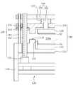
도 1은 본 실시예에 따른 기판합착장치를 나타낸 사시도이고, 도 2는 본 실 시예에 따른 기판합착장치를 나타낸 단면도이다. 도 1 및 도 2를 참조하면, 기판합착장치는 프레임(110), 정렬스테이지(120), 하부챔버(131), 하정반(132), 상부챔버(135), 상정반(136), 상정반지지부(140) 및 구동부(150)를 포함한다.1 is a perspective view showing a substrate bonding apparatus according to the present embodiment, Figure 2 is a cross-sectional view showing a substrate bonding apparatus according to the present embodiment. 1 and 2, the substrate bonding apparatus includes a
프레임(110)은 복수로 마련되어 정렬스테이지(120)와 하부챔버(131)의 테두리부에 배치된다.The
정렬스테이지(120)는 프레임(110)의 내측에 배치되어 프레임(110)에 지지된다. 정렬스테이지(120)는 구동부(150)를 지지하며, 구동부(150)를 도 1에 표기된 x축방향 및 y축방향으로 이동시킨다. 이러한 정렬스테이지(120)는 본 출원인에 의해 출원되어 공개된 "공개번호 10-2006-0055703;기판 합착기"에 개시된 바 있으므로, 상세한 설명은 생략하도록 한다.The
하부챔버(131)는 정렬스테이지(120)의 상측에 배치되어 프레임(110)에 지지된다. 하정반(132)은 하부챔버(131)의 내측에 배치되며, 하부챔버(131)에 지지된다. 하정반(132)은 챔버(130)의 내부로 반입되는 하부기판(S1)을 지지한다.The
상부챔버(135)는 하부챔버(131)의 상측에 배치되며, 하부챔버(131)와 함께 처리공간을 제공한다. 상부챔버(135)는 처리공간(130a)의 개방시 구동부(150)에 의해 지지되고, 처리공간(130a)의 밀폐시 하부챔버(131)에 지지된다. 상정반(136)은 상부챔버(135)의 내측에 배치되며, 상부챔버(135)로부터 이격된다. 도시되지 않았지만 하정반(132) 및 상정반(136)은 기판을 지지하는 진공척, 정전척, 마그네틱척 중 어느 하나를 각각 포함할 수 있다.The
하정반(132)과 상정반의 사이에는 간격감지기(133)가 배치된다. 간격감지 기(133)는 두 기판(S1, S2)의 개략 정렬 이후 두 기판(S1, S2)의 정밀 정렬을 위한 두 기판(S1, S2)의 간격을 감지한다. 간격감지기(133)는 상정반의 승강에 따라 상정반(136)에 접촉되어 접촉신호를 발생시킨다. 이 접촉신호는 이후 설명될 구동모터(151)의 제어신호로 사용된다. 여기서, 도 1 내지 도 2에서는 간격감지기(133)를 접촉식 센서로 도시하고 설명하고 있으나, 다른 실시예로 비접촉식 센서로 채택될 수 있다.The
상정반지지부(140)는 지지판(141)과 지지축(142)을 포함한다. 지지판(141)은 상부챔버(135)의 외측에 배치되며, 상부챔버(135)로부터 이격된다. 지지축(142)은 지지판(141)으로부터 연장되고, 상부챔버(135)를 관통하여 상정반(136)에 체결된다.The upper
구동부(150)는 상부챔버(135)를 승강시켜 처리공간(130a)을 개폐시키며, 상정반지지부(140)를 승강시켜 하부기판(S1)에 대한 상부기판(S2)의 간격을 조절한다. 이러한 구동부(150)는 구동모터(151), 스크류(152), 승강부재(153) 및 승강가이드(154)를 포함한다.The
구동모터(151)는 정렬스테이지(120)에 지지되며, 회전동력을 제공한다. 구동모터는 정회전 및 역회전이 가능하도록 마련된다.The
스크류(152)는 하부챔버(131)와 상부챔버(135)를 관통하며, 지지판(141)에 나사결합되어 지지판(141)을 지지한다. 스크류(152)는 구동모터(151)에 의해 회전되어 지지판(141)을 승강시킨다. 스크류(152)는 구동모터(151)의 정회전에 따라 정회전되어 지지판(141)을 상승시키며, 구동모터(151)의 역회전에 따라 역회전되어 지지판(141)을 하강시킨다.The
승강부재(153)는 상부챔버(135)의 하측에 배치되어 스크류(152)에 나사결합된다. 승강부재(153)는 스크류(152)의 회전에 따라 승강된다. 승강부재(153)는 스크류(152)의 정회전시 상승되어 상부챔버(135)를 지지하여 상부챔버(135)를 상승시키며, 스크류(152)의 역회전시 하강되어 상부챔버(135)를 하부챔버(131) 측으로 하강시킨다.The
승강부재(153)와 상부챔버(135)의 사이에는 완충부재(155)가 배치된다. 완충부재(155)는 스크류(152)의 회전에 따라 서로 접촉되는 상부챔버(135)와 승강부재(153)에 발생될 수 있는 충격을 완화시키며, 상부챔버(135) 및 승강부재(153)의 마모를 방지한다.A
승강가이드(154)는 하부챔버(131)에 고정되며, 승강부재(153), 상부챔버(135) 및 상정반지지부(140)를 관통한다. 승강가이드(154)는 스크류(152)에 나사결합된 상부챔버(135) 및 승강부재(153)가 스크류(152)의 회전에 따라 회전되지 않도록 하며, 상부챔버(135)와 승강부재(153)의 승강을 안내한다.The
한편, 하부챔버(131)와 상부챔버(135)의 사이에는 처리공간(130a)의 밀폐시 하부챔버(131)와 상부챔버(135)의 사이로 처리공간(130a)의 기밀이 새어나가는 것을 방지하는 제1 기밀부재(134)가 배치된다. 제1 기밀부재(134)로는 오-링이 사용된다.Meanwhile, between the
또한, 지지판(141)과 상부챔버(135)의 사이에는 처리공간(130a)의 밀폐시 지지축(142)이 관통되는 관통홀(142a)로부터 처리공간(130a)의 기밀이 새어나가는 것 을 방지하는 제2 기밀부재(137)가 배치된다. 제2 기밀부재(137)로는 벨로우즈가 사용된다.In addition, between the supporting
도시되지 않았지만, 하부기판(S1)과 상부기판(S2)에는 두 기판(S1, S2)의 정렬을 위한 얼라인마크가 각각 형성되어 제공될 수 있으며, 기판합착장치는 두 얼라인마크의 일치여부를 촬영하는 카메라를 포함할 수 있다. 이러한 얼라인마크 및 카메라는 이미 공지된 기술이므로 상세한 설명은 생략하도록 한다.Although not shown, an alignment mark for aligning the two substrates S1 and S2 may be provided on the lower substrate S1 and the upper substrate S2, respectively, and the substrate bonding apparatus may be aligned with the two alignment marks. It may include a camera for photographing. Since the alignment mark and the camera are already known technologies, detailed descriptions thereof will be omitted.
이하, 본 실시예에 따른 기판처리장치의 작동에 대해 첨부된 도면을 참조하여 상세히 설명하도록 한다.Hereinafter, the operation of the substrate treating apparatus according to the present embodiment will be described in detail with reference to the accompanying drawings.
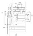
도 3은 본 실시예에 따른 기판처리장치에서 처리공간이 개방된 상태를 나타낸 부분단면도이다. 도 3을 참조하면, 상부챔버(135)는 승강부재(153)에 지지되어 하부챔버(131)로부터 이격된다. 상부챔버(135)가 하부챔버(131)로부터 이격됨에 따라 처리공간(130a)은 개방된다. 개방된 처리공간(130a)으로 하부기판(S1)과 상부기판(S2)이 반입된다. 하부기판(S1)은 하정반(132)에 지지되고 상부기판(S2)은 상정반(136)에 지지되어 서로 대향한다.3 is a partial cross-sectional view showing a state in which a processing space is opened in the substrate processing apparatus according to the present embodiment. Referring to FIG. 3, the
도 4는 본 실시예에 따른 기판처리장치의 처리공간 밀폐 작동을 나타낸 부분단면도이다. 도 4를 참조하면, 처리공간(130a)의 밀폐를 위해 구동모터(151)는 스크류(152)를 역회전시킨다. 스크류(152)가 역회전됨에 따라 지지판(141)과 승강부재(153)는 함께 하강한다. 이때 승강가이드(154)는 지지판(141)과 승강부재(153)의 회전을 방지하며, 지지판(141)과 승강부재(153)의 하강을 안내한다.4 is a partial sectional view showing a process space sealing operation of the substrate processing apparatus according to the present embodiment. Referring to FIG. 4, the
승강부재(153)에 지지되는 상부챔버(135)는 승강부재(153)와 함께 하강된다. 상부챔버(135)는 제1 기밀부재(134)에 접촉되며, 하부챔버(131)에 의해 지지된다. 이와 같이 상부챔버(135)의 하강에 따라 처리공간(130a)은 밀폐되며 제1 기밀부재(134)는 처리공간(130a)의 기밀을 유지시킨다.The
처리공간(130a)이 밀폐되면 두 기판(S1, S2)의 개략 정렬이 이루어진다. 즉, 카메라(미도시)는 두 얼라인마크(미도시)의 일치 여부를 촬영한다. 카메라(미도시)의 촬영결과에 따라 정렬스테이지(120)는 구동부(150)를 평면 상(x축방향 또는, y축방향)으로 이동시킨다. 구동부(150)의 위치가 이동됨에 따라 스크류(152)에 지지되는 지지판(141)의 위치가 이동되고, 지지판(141)의 위치가 이동됨에 따라 지지축(142)에 의해 지지되는 상정반(136)의 위치가 이동된다.When the
이와 같이 상정반(136)의 위치를 조절하여 하정반(132)에 지지되는 하부기판(S1)에 대한 상부기판(S2)의 위치를 조절하여 두 기판을 정렬한다. (이하, 기판 정렬동작)As such, by adjusting the position of the
도 5는 본 실시예에 따른 기판처리장치의 기판 간격조절 작동을 나타낸 부분단면도이다. 도 5를 참조하면, 두 기판(S1, S2)의 정밀 정렬을 위해 구동모터(151)는 스크류(152)를 역회전시킨다. 스크류(152)가 역회전됨에 따라 지지판(141)과 승강부재(153)는 함께 하강한다. 이때 승강가이드(154)는 지지판(141)과 승강부재(153)의 회전을 방지하며, 지지판(141)과 승강부재(153)의 하강을 안내한다.5 is a partial cross-sectional view showing a substrate gap adjusting operation of the substrate processing apparatus according to the present embodiment. Referring to FIG. 5, the
상부챔버(135)는 하부챔버(131)에 의해 지지된 상태이므로, 승강부재(153)는 하강되어 상부챔버(135)로부터 이격된다. 지지판(141)이 하강됨에 따라 지지 축(142)에 의해 지지되는 상정반(136)은 함께 하강한다. 상정반(136)이 하강됨에 따라 상정반(136)은 하정반(132)에 배치된 간격감지기(133)에 접촉된다. 간격감지기(133)는 접촉신호를 발생하며, 구동모터(151)는 접촉신호의 발생에 따라 회전이 정지된다. 이때 두 기판(S1, S2)의 간격은 수 ㎛ ~ 수백 ㎛ 로 형성된다.Since the
이와 같이 두 기판(S1, S2)이 근접하면 상술한 기판 정렬동작에 따라 두 기판의 정밀 정렬이 이루어진다.As such, when the two substrates S1 and S2 are close to each other, precise alignment of the two substrates is performed according to the substrate alignment operation described above.
두 기판(S1, S2)의 정밀 정렬이 이루어지면, 상정반(136)은 상부기판(S2)의 지지상태를 해제한다. 상부기판(S2)은 하부기판(S1)으로 자유낙하하여 하부기판(S1)에 접촉되고, 두 기판(S1, S2)은 합착된다.When the precise alignment of the two substrates (S1, S2) is made, the
도 6은 본 실시예에 따른 기판처리장치의 처리공간 개방 동작을 나타낸 부분단면도이다. 도 6을 참조하면, 합착된 두 기판(S1, S2)의 반출을 위해 구동모터(151)는 스크류(152)를 정회전시킨다. 스크류(152)가 정회전됨에 따라 지지판(141)과 승강부재(153)는 함께 상승한다. 이때 승강가이드(154)는 지지판(141)과 승강부재(153)의 회전을 방지하며, 지지판(141)과 승강부재(153)의 상승을 안내한다.6 is a partial cross-sectional view showing a processing space opening operation of the substrate processing apparatus according to the present embodiment. Referring to FIG. 6, the driving
스크류(152)의 정회전에 의해 상승하는 승강부재(153)는 상부챔버(135)에 접촉된다. 이때 완충부재(155)는 서로 접촉되는 상부챔버(135)와 승강부재(153)에 발생될 수 있는 충격을 완화시키며, 상부챔버(135) 및 승강부재(153)의 마모를 방지한다.The elevating
상부챔버(135)에 접촉된 승강부재(153)는 스크류(152)의 정회전에 따라 계속 해서 상승하며, 상부챔버(135)는 승강부재(153)에 지지되어 승강부재(153)와 함께 상승한다. 상부챔버(135)의 상승에 따라 처리공간(130a)은 개방된다.The elevating
이후, 합착된 두 기판(S1, S2)은 개방된 처리공간(130a)의 외부로 반출된다.Thereafter, the two bonded substrates S1 and S2 are carried out of the
상술한 바와 같이 기판합착장치는 구동부(150)에 의해 처리공간(130a)의 개폐와 두 기판(S1, S2)의 간격조절을 수행할 수 있다.As described above, the substrate bonding apparatus may perform opening / closing of the
도 1은 본 실시예에 따른 기판합착장치를 나타낸 사시도이다.1 is a perspective view showing a substrate bonding apparatus according to the present embodiment.
도 2는 본 실시예에 따른 기판합착장치를 나타낸 단면도이다.2 is a cross-sectional view showing a substrate bonding apparatus according to the present embodiment.
도 3은 본 실시예에 따른 기판처리장치에서 처리공간이 개방된 상태를 나타낸 부분단면도이다.3 is a partial cross-sectional view showing a state in which a processing space is opened in the substrate processing apparatus according to the present embodiment.
도 4는 본 실시예에 따른 기판처리장치의 처리공간 밀폐 작동을 나타낸 부분단면도이다.4 is a partial sectional view showing a process space sealing operation of the substrate processing apparatus according to the present embodiment.
도 5는 본 실시예에 따른 기판처리장치의 기판 간격조절 작동을 나타낸 부분단면도이다.5 is a partial cross-sectional view showing a substrate gap adjusting operation of the substrate processing apparatus according to the present embodiment.
도 6은 본 실시예에 따른 기판처리장치의 처리공간 개방 동작을 나타낸 부분단면도이다.6 is a partial cross-sectional view showing a processing space opening operation of the substrate processing apparatus according to the present embodiment.
<도면의 주요부분에 대한 부호 설명>Description of the Related Art [0002]
110 : 프레임120 : 정렬스테이지110: frame 120: alignment stage
130 : 챔버131 : 하부챔버130: chamber 131: lower chamber
135 : 상부챔버136 : 상정반135: upper chamber 136: upper plate
140 : 상정반지지부141 : 지지판140: upper plate support 141: support plate
142 : 지지축150 : 구동부142: support shaft 150: drive unit
152 : 스크류154 : 승강부재152: screw 154: lifting member
Claims (8)
Translated fromKoreanPriority Applications (1)
| Application Number | Priority Date | Filing Date | Title |
|---|---|---|---|
| KR1020080138517AKR101111063B1 (en) | 2008-12-31 | 2008-12-31 | Apparatus for joining of substrate |
Applications Claiming Priority (1)
| Application Number | Priority Date | Filing Date | Title |
|---|---|---|---|
| KR1020080138517AKR101111063B1 (en) | 2008-12-31 | 2008-12-31 | Apparatus for joining of substrate |
Publications (2)
| Publication Number | Publication Date |
|---|---|
| KR20100079920A KR20100079920A (en) | 2010-07-08 |
| KR101111063B1true KR101111063B1 (en) | 2012-02-16 |
Family
ID=42640957
Family Applications (1)
| Application Number | Title | Priority Date | Filing Date |
|---|---|---|---|
| KR1020080138517AExpired - Fee RelatedKR101111063B1 (en) | 2008-12-31 | 2008-12-31 | Apparatus for joining of substrate |
Country Status (1)
| Country | Link |
|---|---|
| KR (1) | KR101111063B1 (en) |
Cited By (1)
| Publication number | Priority date | Publication date | Assignee | Title |
|---|---|---|---|---|
| US11728200B2 (en) | 2019-05-23 | 2023-08-15 | Samsung Electronics Co., Ltd. | Wafer bonding apparatuses |
Families Citing this family (318)
| Publication number | Priority date | Publication date | Assignee | Title |
|---|---|---|---|---|
| US9394608B2 (en) | 2009-04-06 | 2016-07-19 | Asm America, Inc. | Semiconductor processing reactor and components thereof |
| US8802201B2 (en) | 2009-08-14 | 2014-08-12 | Asm America, Inc. | Systems and methods for thin-film deposition of metal oxides using excited nitrogen-oxygen species |
| US9312155B2 (en) | 2011-06-06 | 2016-04-12 | Asm Japan K.K. | High-throughput semiconductor-processing apparatus equipped with multiple dual-chamber modules |
| US10854498B2 (en) | 2011-07-15 | 2020-12-01 | Asm Ip Holding B.V. | Wafer-supporting device and method for producing same |
| US20130023129A1 (en) | 2011-07-20 | 2013-01-24 | Asm America, Inc. | Pressure transmitter for a semiconductor processing environment |
| US9017481B1 (en) | 2011-10-28 | 2015-04-28 | Asm America, Inc. | Process feed management for semiconductor substrate processing |
| US10714315B2 (en) | 2012-10-12 | 2020-07-14 | Asm Ip Holdings B.V. | Semiconductor reaction chamber showerhead |
| KR101540054B1 (en)* | 2012-12-28 | 2015-07-29 | 엘아이지인베니아 주식회사 | Method and apparatus for bonding substrates |
| US20160376700A1 (en) | 2013-02-01 | 2016-12-29 | Asm Ip Holding B.V. | System for treatment of deposition reactor |
| US10683571B2 (en) | 2014-02-25 | 2020-06-16 | Asm Ip Holding B.V. | Gas supply manifold and method of supplying gases to chamber using same |
| US10167557B2 (en) | 2014-03-18 | 2019-01-01 | Asm Ip Holding B.V. | Gas distribution system, reactor including the system, and methods of using the same |
| US11015245B2 (en) | 2014-03-19 | 2021-05-25 | Asm Ip Holding B.V. | Gas-phase reactor and system having exhaust plenum and components thereof |
| US10858737B2 (en) | 2014-07-28 | 2020-12-08 | Asm Ip Holding B.V. | Showerhead assembly and components thereof |
| US9890456B2 (en) | 2014-08-21 | 2018-02-13 | Asm Ip Holding B.V. | Method and system for in situ formation of gas-phase compounds |
| US9657845B2 (en) | 2014-10-07 | 2017-05-23 | Asm Ip Holding B.V. | Variable conductance gas distribution apparatus and method |
| US10941490B2 (en) | 2014-10-07 | 2021-03-09 | Asm Ip Holding B.V. | Multiple temperature range susceptor, assembly, reactor and system including the susceptor, and methods of using the same |
| US10276355B2 (en) | 2015-03-12 | 2019-04-30 | Asm Ip Holding B.V. | Multi-zone reactor, system including the reactor, and method of using the same |
| US10458018B2 (en) | 2015-06-26 | 2019-10-29 | Asm Ip Holding B.V. | Structures including metal carbide material, devices including the structures, and methods of forming same |
| US10600673B2 (en) | 2015-07-07 | 2020-03-24 | Asm Ip Holding B.V. | Magnetic susceptor to baseplate seal |
| US10211308B2 (en) | 2015-10-21 | 2019-02-19 | Asm Ip Holding B.V. | NbMC layers |
| US11139308B2 (en) | 2015-12-29 | 2021-10-05 | Asm Ip Holding B.V. | Atomic layer deposition of III-V compounds to form V-NAND devices |
| US10529554B2 (en) | 2016-02-19 | 2020-01-07 | Asm Ip Holding B.V. | Method for forming silicon nitride film selectively on sidewalls or flat surfaces of trenches |
| US10343920B2 (en) | 2016-03-18 | 2019-07-09 | Asm Ip Holding B.V. | Aligned carbon nanotubes |
| US10865475B2 (en) | 2016-04-21 | 2020-12-15 | Asm Ip Holding B.V. | Deposition of metal borides and silicides |
| US10190213B2 (en) | 2016-04-21 | 2019-01-29 | Asm Ip Holding B.V. | Deposition of metal borides |
| US10032628B2 (en) | 2016-05-02 | 2018-07-24 | Asm Ip Holding B.V. | Source/drain performance through conformal solid state doping |
| US10367080B2 (en) | 2016-05-02 | 2019-07-30 | Asm Ip Holding B.V. | Method of forming a germanium oxynitride film |
| US11453943B2 (en) | 2016-05-25 | 2022-09-27 | Asm Ip Holding B.V. | Method for forming carbon-containing silicon/metal oxide or nitride film by ALD using silicon precursor and hydrocarbon precursor |
| US10612137B2 (en) | 2016-07-08 | 2020-04-07 | Asm Ip Holdings B.V. | Organic reactants for atomic layer deposition |
| US9859151B1 (en) | 2016-07-08 | 2018-01-02 | Asm Ip Holding B.V. | Selective film deposition method to form air gaps |
| US10714385B2 (en) | 2016-07-19 | 2020-07-14 | Asm Ip Holding B.V. | Selective deposition of tungsten |
| KR102532607B1 (en)* | 2016-07-28 | 2023-05-15 | 에이에스엠 아이피 홀딩 비.브이. | Substrate processing apparatus and method of operating the same |
| US9887082B1 (en) | 2016-07-28 | 2018-02-06 | Asm Ip Holding B.V. | Method and apparatus for filling a gap |
| US9812320B1 (en) | 2016-07-28 | 2017-11-07 | Asm Ip Holding B.V. | Method and apparatus for filling a gap |
| US10643826B2 (en) | 2016-10-26 | 2020-05-05 | Asm Ip Holdings B.V. | Methods for thermally calibrating reaction chambers |
| US11532757B2 (en) | 2016-10-27 | 2022-12-20 | Asm Ip Holding B.V. | Deposition of charge trapping layers |
| US10714350B2 (en) | 2016-11-01 | 2020-07-14 | ASM IP Holdings, B.V. | Methods for forming a transition metal niobium nitride film on a substrate by atomic layer deposition and related semiconductor device structures |
| US10643904B2 (en) | 2016-11-01 | 2020-05-05 | Asm Ip Holdings B.V. | Methods for forming a semiconductor device and related semiconductor device structures |
| US10229833B2 (en) | 2016-11-01 | 2019-03-12 | Asm Ip Holding B.V. | Methods for forming a transition metal nitride film on a substrate by atomic layer deposition and related semiconductor device structures |
| US10134757B2 (en) | 2016-11-07 | 2018-11-20 | Asm Ip Holding B.V. | Method of processing a substrate and a device manufactured by using the method |
| KR102546317B1 (en) | 2016-11-15 | 2023-06-21 | 에이에스엠 아이피 홀딩 비.브이. | Gas supply unit and substrate processing apparatus including the same |
| KR102762543B1 (en) | 2016-12-14 | 2025-02-05 | 에이에스엠 아이피 홀딩 비.브이. | Substrate processing apparatus |
| US11447861B2 (en) | 2016-12-15 | 2022-09-20 | Asm Ip Holding B.V. | Sequential infiltration synthesis apparatus and a method of forming a patterned structure |
| US11581186B2 (en) | 2016-12-15 | 2023-02-14 | Asm Ip Holding B.V. | Sequential infiltration synthesis apparatus |
| KR102700194B1 (en) | 2016-12-19 | 2024-08-28 | 에이에스엠 아이피 홀딩 비.브이. | Substrate processing apparatus |
| US10269558B2 (en) | 2016-12-22 | 2019-04-23 | Asm Ip Holding B.V. | Method of forming a structure on a substrate |
| US10867788B2 (en) | 2016-12-28 | 2020-12-15 | Asm Ip Holding B.V. | Method of forming a structure on a substrate |
| US11390950B2 (en) | 2017-01-10 | 2022-07-19 | Asm Ip Holding B.V. | Reactor system and method to reduce residue buildup during a film deposition process |
| US10655221B2 (en) | 2017-02-09 | 2020-05-19 | Asm Ip Holding B.V. | Method for depositing oxide film by thermal ALD and PEALD |
| US10468261B2 (en) | 2017-02-15 | 2019-11-05 | Asm Ip Holding B.V. | Methods for forming a metallic film on a substrate by cyclical deposition and related semiconductor device structures |
| US10529563B2 (en) | 2017-03-29 | 2020-01-07 | Asm Ip Holdings B.V. | Method for forming doped metal oxide films on a substrate by cyclical deposition and related semiconductor device structures |
| USD876504S1 (en) | 2017-04-03 | 2020-02-25 | Asm Ip Holding B.V. | Exhaust flow control ring for semiconductor deposition apparatus |
| KR102457289B1 (en) | 2017-04-25 | 2022-10-21 | 에이에스엠 아이피 홀딩 비.브이. | Method for depositing a thin film and manufacturing a semiconductor device |
| US10770286B2 (en) | 2017-05-08 | 2020-09-08 | Asm Ip Holdings B.V. | Methods for selectively forming a silicon nitride film on a substrate and related semiconductor device structures |
| US10892156B2 (en) | 2017-05-08 | 2021-01-12 | Asm Ip Holding B.V. | Methods for forming a silicon nitride film on a substrate and related semiconductor device structures |
| US12040200B2 (en) | 2017-06-20 | 2024-07-16 | Asm Ip Holding B.V. | Semiconductor processing apparatus and methods for calibrating a semiconductor processing apparatus |
| US11306395B2 (en) | 2017-06-28 | 2022-04-19 | Asm Ip Holding B.V. | Methods for depositing a transition metal nitride film on a substrate by atomic layer deposition and related deposition apparatus |
| US10685834B2 (en) | 2017-07-05 | 2020-06-16 | Asm Ip Holdings B.V. | Methods for forming a silicon germanium tin layer and related semiconductor device structures |
| KR20190009245A (en) | 2017-07-18 | 2019-01-28 | 에이에스엠 아이피 홀딩 비.브이. | Methods for forming a semiconductor device structure and related semiconductor device structures |
| US11374112B2 (en) | 2017-07-19 | 2022-06-28 | Asm Ip Holding B.V. | Method for depositing a group IV semiconductor and related semiconductor device structures |
| US10541333B2 (en) | 2017-07-19 | 2020-01-21 | Asm Ip Holding B.V. | Method for depositing a group IV semiconductor and related semiconductor device structures |
| US11018002B2 (en) | 2017-07-19 | 2021-05-25 | Asm Ip Holding B.V. | Method for selectively depositing a Group IV semiconductor and related semiconductor device structures |
| US10590535B2 (en)* | 2017-07-26 | 2020-03-17 | Asm Ip Holdings B.V. | Chemical treatment, deposition and/or infiltration apparatus and method for using the same |
| TWI815813B (en) | 2017-08-04 | 2023-09-21 | 荷蘭商Asm智慧財產控股公司 | Showerhead assembly for distributing a gas within a reaction chamber |
| US10770336B2 (en) | 2017-08-08 | 2020-09-08 | Asm Ip Holding B.V. | Substrate lift mechanism and reactor including same |
| US10692741B2 (en) | 2017-08-08 | 2020-06-23 | Asm Ip Holdings B.V. | Radiation shield |
| US11769682B2 (en) | 2017-08-09 | 2023-09-26 | Asm Ip Holding B.V. | Storage apparatus for storing cassettes for substrates and processing apparatus equipped therewith |
| US10249524B2 (en) | 2017-08-09 | 2019-04-02 | Asm Ip Holding B.V. | Cassette holder assembly for a substrate cassette and holding member for use in such assembly |
| US11139191B2 (en) | 2017-08-09 | 2021-10-05 | Asm Ip Holding B.V. | Storage apparatus for storing cassettes for substrates and processing apparatus equipped therewith |
| USD900036S1 (en) | 2017-08-24 | 2020-10-27 | Asm Ip Holding B.V. | Heater electrical connector and adapter |
| US11830730B2 (en) | 2017-08-29 | 2023-11-28 | Asm Ip Holding B.V. | Layer forming method and apparatus |
| US11056344B2 (en) | 2017-08-30 | 2021-07-06 | Asm Ip Holding B.V. | Layer forming method |
| US11295980B2 (en) | 2017-08-30 | 2022-04-05 | Asm Ip Holding B.V. | Methods for depositing a molybdenum metal film over a dielectric surface of a substrate by a cyclical deposition process and related semiconductor device structures |
| KR102491945B1 (en) | 2017-08-30 | 2023-01-26 | 에이에스엠 아이피 홀딩 비.브이. | Substrate processing apparatus |
| KR102401446B1 (en) | 2017-08-31 | 2022-05-24 | 에이에스엠 아이피 홀딩 비.브이. | Substrate processing apparatus |
| KR102630301B1 (en) | 2017-09-21 | 2024-01-29 | 에이에스엠 아이피 홀딩 비.브이. | Method of sequential infiltration synthesis treatment of infiltrateable material and structures and devices formed using same |
| US10844484B2 (en) | 2017-09-22 | 2020-11-24 | Asm Ip Holding B.V. | Apparatus for dispensing a vapor phase reactant to a reaction chamber and related methods |
| US10658205B2 (en) | 2017-09-28 | 2020-05-19 | Asm Ip Holdings B.V. | Chemical dispensing apparatus and methods for dispensing a chemical to a reaction chamber |
| US10403504B2 (en) | 2017-10-05 | 2019-09-03 | Asm Ip Holding B.V. | Method for selectively depositing a metallic film on a substrate |
| US10319588B2 (en) | 2017-10-10 | 2019-06-11 | Asm Ip Holding B.V. | Method for depositing a metal chalcogenide on a substrate by cyclical deposition |
| US10923344B2 (en) | 2017-10-30 | 2021-02-16 | Asm Ip Holding B.V. | Methods for forming a semiconductor structure and related semiconductor structures |
| US10910262B2 (en) | 2017-11-16 | 2021-02-02 | Asm Ip Holding B.V. | Method of selectively depositing a capping layer structure on a semiconductor device structure |
| KR102443047B1 (en) | 2017-11-16 | 2022-09-14 | 에이에스엠 아이피 홀딩 비.브이. | Method of processing a substrate and a device manufactured by the same |
| US11022879B2 (en) | 2017-11-24 | 2021-06-01 | Asm Ip Holding B.V. | Method of forming an enhanced unexposed photoresist layer |
| WO2019103613A1 (en) | 2017-11-27 | 2019-05-31 | Asm Ip Holding B.V. | A storage device for storing wafer cassettes for use with a batch furnace |
| CN111344522B (en) | 2017-11-27 | 2022-04-12 | 阿斯莫Ip控股公司 | Including clean mini-environment device |
| US10872771B2 (en) | 2018-01-16 | 2020-12-22 | Asm Ip Holding B. V. | Method for depositing a material film on a substrate within a reaction chamber by a cyclical deposition process and related device structures |
| TWI799494B (en) | 2018-01-19 | 2023-04-21 | 荷蘭商Asm 智慧財產控股公司 | Deposition method |
| KR102695659B1 (en) | 2018-01-19 | 2024-08-14 | 에이에스엠 아이피 홀딩 비.브이. | Method for depositing a gap filling layer by plasma assisted deposition |
| USD903477S1 (en) | 2018-01-24 | 2020-12-01 | Asm Ip Holdings B.V. | Metal clamp |
| US11018047B2 (en) | 2018-01-25 | 2021-05-25 | Asm Ip Holding B.V. | Hybrid lift pin |
| KR102455643B1 (en)* | 2018-01-26 | 2022-10-19 | 주식회사 케이씨텍 | Apparatus for Treating Substrate and the Method Thereof |
| USD880437S1 (en) | 2018-02-01 | 2020-04-07 | Asm Ip Holding B.V. | Gas supply plate for semiconductor manufacturing apparatus |
| US11081345B2 (en) | 2018-02-06 | 2021-08-03 | Asm Ip Holding B.V. | Method of post-deposition treatment for silicon oxide film |
| US10896820B2 (en) | 2018-02-14 | 2021-01-19 | Asm Ip Holding B.V. | Method for depositing a ruthenium-containing film on a substrate by a cyclical deposition process |
| WO2019158960A1 (en) | 2018-02-14 | 2019-08-22 | Asm Ip Holding B.V. | A method for depositing a ruthenium-containing film on a substrate by a cyclical deposition process |
| US10731249B2 (en) | 2018-02-15 | 2020-08-04 | Asm Ip Holding B.V. | Method of forming a transition metal containing film on a substrate by a cyclical deposition process, a method for supplying a transition metal halide compound to a reaction chamber, and related vapor deposition apparatus |
| KR102636427B1 (en) | 2018-02-20 | 2024-02-13 | 에이에스엠 아이피 홀딩 비.브이. | Substrate processing method and apparatus |
| US10658181B2 (en) | 2018-02-20 | 2020-05-19 | Asm Ip Holding B.V. | Method of spacer-defined direct patterning in semiconductor fabrication |
| US10975470B2 (en) | 2018-02-23 | 2021-04-13 | Asm Ip Holding B.V. | Apparatus for detecting or monitoring for a chemical precursor in a high temperature environment |
| US11473195B2 (en) | 2018-03-01 | 2022-10-18 | Asm Ip Holding B.V. | Semiconductor processing apparatus and a method for processing a substrate |
| US11629406B2 (en) | 2018-03-09 | 2023-04-18 | Asm Ip Holding B.V. | Semiconductor processing apparatus comprising one or more pyrometers for measuring a temperature of a substrate during transfer of the substrate |
| US11114283B2 (en) | 2018-03-16 | 2021-09-07 | Asm Ip Holding B.V. | Reactor, system including the reactor, and methods of manufacturing and using same |
| KR102646467B1 (en) | 2018-03-27 | 2024-03-11 | 에이에스엠 아이피 홀딩 비.브이. | Method of forming an electrode on a substrate and a semiconductor device structure including an electrode |
| US11230766B2 (en) | 2018-03-29 | 2022-01-25 | Asm Ip Holding B.V. | Substrate processing apparatus and method |
| US11088002B2 (en) | 2018-03-29 | 2021-08-10 | Asm Ip Holding B.V. | Substrate rack and a substrate processing system and method |
| KR102501472B1 (en) | 2018-03-30 | 2023-02-20 | 에이에스엠 아이피 홀딩 비.브이. | Substrate processing method |
| KR102600229B1 (en) | 2018-04-09 | 2023-11-10 | 에이에스엠 아이피 홀딩 비.브이. | Substrate supporting device, substrate processing apparatus including the same and substrate processing method |
| TWI811348B (en) | 2018-05-08 | 2023-08-11 | 荷蘭商Asm 智慧財產控股公司 | Methods for depositing an oxide film on a substrate by a cyclical deposition process and related device structures |
| US12025484B2 (en) | 2018-05-08 | 2024-07-02 | Asm Ip Holding B.V. | Thin film forming method |
| US12272527B2 (en) | 2018-05-09 | 2025-04-08 | Asm Ip Holding B.V. | Apparatus for use with hydrogen radicals and method of using same |
| KR20190129718A (en) | 2018-05-11 | 2019-11-20 | 에이에스엠 아이피 홀딩 비.브이. | Methods for forming a doped metal carbide film on a substrate and related semiconductor device structures |
| KR102596988B1 (en) | 2018-05-28 | 2023-10-31 | 에이에스엠 아이피 홀딩 비.브이. | Method of processing a substrate and a device manufactured by the same |
| US11718913B2 (en) | 2018-06-04 | 2023-08-08 | Asm Ip Holding B.V. | Gas distribution system and reactor system including same |
| TWI840362B (en) | 2018-06-04 | 2024-05-01 | 荷蘭商Asm Ip私人控股有限公司 | Wafer handling chamber with moisture reduction |
| US11286562B2 (en) | 2018-06-08 | 2022-03-29 | Asm Ip Holding B.V. | Gas-phase chemical reactor and method of using same |
| KR102568797B1 (en) | 2018-06-21 | 2023-08-21 | 에이에스엠 아이피 홀딩 비.브이. | Substrate processing system |
| US10797133B2 (en) | 2018-06-21 | 2020-10-06 | Asm Ip Holding B.V. | Method for depositing a phosphorus doped silicon arsenide film and related semiconductor device structures |
| KR102854019B1 (en) | 2018-06-27 | 2025-09-02 | 에이에스엠 아이피 홀딩 비.브이. | Periodic deposition method for forming a metal-containing material and films and structures comprising the metal-containing material |
| TWI873894B (en) | 2018-06-27 | 2025-02-21 | 荷蘭商Asm Ip私人控股有限公司 | Cyclic deposition methods for forming metal-containing material and films and structures including the metal-containing material |
| KR102686758B1 (en) | 2018-06-29 | 2024-07-18 | 에이에스엠 아이피 홀딩 비.브이. | Method for depositing a thin film and manufacturing a semiconductor device |
| US10612136B2 (en) | 2018-06-29 | 2020-04-07 | ASM IP Holding, B.V. | Temperature-controlled flange and reactor system including same |
| US10755922B2 (en) | 2018-07-03 | 2020-08-25 | Asm Ip Holding B.V. | Method for depositing silicon-free carbon-containing film as gap-fill layer by pulse plasma-assisted deposition |
| US10388513B1 (en) | 2018-07-03 | 2019-08-20 | Asm Ip Holding B.V. | Method for depositing silicon-free carbon-containing film as gap-fill layer by pulse plasma-assisted deposition |
| US10767789B2 (en) | 2018-07-16 | 2020-09-08 | Asm Ip Holding B.V. | Diaphragm valves, valve components, and methods for forming valve components |
| US11053591B2 (en) | 2018-08-06 | 2021-07-06 | Asm Ip Holding B.V. | Multi-port gas injection system and reactor system including same |
| US10883175B2 (en) | 2018-08-09 | 2021-01-05 | Asm Ip Holding B.V. | Vertical furnace for processing substrates and a liner for use therein |
| US10829852B2 (en) | 2018-08-16 | 2020-11-10 | Asm Ip Holding B.V. | Gas distribution device for a wafer processing apparatus |
| US11430674B2 (en) | 2018-08-22 | 2022-08-30 | Asm Ip Holding B.V. | Sensor array, apparatus for dispensing a vapor phase reactant to a reaction chamber and related methods |
| KR102707956B1 (en) | 2018-09-11 | 2024-09-19 | 에이에스엠 아이피 홀딩 비.브이. | Method for deposition of a thin film |
| US11024523B2 (en) | 2018-09-11 | 2021-06-01 | Asm Ip Holding B.V. | Substrate processing apparatus and method |
| US11049751B2 (en) | 2018-09-14 | 2021-06-29 | Asm Ip Holding B.V. | Cassette supply system to store and handle cassettes and processing apparatus equipped therewith |
| CN110970344B (en) | 2018-10-01 | 2024-10-25 | Asmip控股有限公司 | Substrate holding apparatus, system comprising the same and method of using the same |
| US11232963B2 (en) | 2018-10-03 | 2022-01-25 | Asm Ip Holding B.V. | Substrate processing apparatus and method |
| KR102592699B1 (en) | 2018-10-08 | 2023-10-23 | 에이에스엠 아이피 홀딩 비.브이. | Substrate support unit and apparatuses for depositing thin film and processing the substrate including the same |
| US10847365B2 (en) | 2018-10-11 | 2020-11-24 | Asm Ip Holding B.V. | Method of forming conformal silicon carbide film by cyclic CVD |
| US10811256B2 (en) | 2018-10-16 | 2020-10-20 | Asm Ip Holding B.V. | Method for etching a carbon-containing feature |
| KR102605121B1 (en) | 2018-10-19 | 2023-11-23 | 에이에스엠 아이피 홀딩 비.브이. | Substrate processing apparatus and substrate processing method |
| KR102546322B1 (en) | 2018-10-19 | 2023-06-21 | 에이에스엠 아이피 홀딩 비.브이. | Substrate processing apparatus and substrate processing method |
| USD948463S1 (en) | 2018-10-24 | 2022-04-12 | Asm Ip Holding B.V. | Susceptor for semiconductor substrate supporting apparatus |
| US12378665B2 (en) | 2018-10-26 | 2025-08-05 | Asm Ip Holding B.V. | High temperature coatings for a preclean and etch apparatus and related methods |
| US11087997B2 (en) | 2018-10-31 | 2021-08-10 | Asm Ip Holding B.V. | Substrate processing apparatus for processing substrates |
| KR102748291B1 (en) | 2018-11-02 | 2024-12-31 | 에이에스엠 아이피 홀딩 비.브이. | Substrate support unit and substrate processing apparatus including the same |
| US11572620B2 (en) | 2018-11-06 | 2023-02-07 | Asm Ip Holding B.V. | Methods for selectively depositing an amorphous silicon film on a substrate |
| US11031242B2 (en) | 2018-11-07 | 2021-06-08 | Asm Ip Holding B.V. | Methods for depositing a boron doped silicon germanium film |
| US10847366B2 (en) | 2018-11-16 | 2020-11-24 | Asm Ip Holding B.V. | Methods for depositing a transition metal chalcogenide film on a substrate by a cyclical deposition process |
| US10818758B2 (en) | 2018-11-16 | 2020-10-27 | Asm Ip Holding B.V. | Methods for forming a metal silicate film on a substrate in a reaction chamber and related semiconductor device structures |
| US10559458B1 (en) | 2018-11-26 | 2020-02-11 | Asm Ip Holding B.V. | Method of forming oxynitride film |
| US12040199B2 (en) | 2018-11-28 | 2024-07-16 | Asm Ip Holding B.V. | Substrate processing apparatus for processing substrates |
| US11217444B2 (en) | 2018-11-30 | 2022-01-04 | Asm Ip Holding B.V. | Method for forming an ultraviolet radiation responsive metal oxide-containing film |
| KR102636428B1 (en) | 2018-12-04 | 2024-02-13 | 에이에스엠 아이피 홀딩 비.브이. | A method for cleaning a substrate processing apparatus |
| US11158513B2 (en) | 2018-12-13 | 2021-10-26 | Asm Ip Holding B.V. | Methods for forming a rhenium-containing film on a substrate by a cyclical deposition process and related semiconductor device structures |
| TWI874340B (en) | 2018-12-14 | 2025-03-01 | 荷蘭商Asm Ip私人控股有限公司 | Method of forming device structure, structure formed by the method and system for performing the method |
| TWI866480B (en) | 2019-01-17 | 2024-12-11 | 荷蘭商Asm Ip 私人控股有限公司 | Methods of forming a transition metal containing film on a substrate by a cyclical deposition process |
| KR102727227B1 (en) | 2019-01-22 | 2024-11-07 | 에이에스엠 아이피 홀딩 비.브이. | Semiconductor processing device |
| CN111524788B (en) | 2019-02-01 | 2023-11-24 | Asm Ip私人控股有限公司 | Method for forming topologically selective films of silicon oxide |
| TWI838458B (en) | 2019-02-20 | 2024-04-11 | 荷蘭商Asm Ip私人控股有限公司 | Apparatus and methods for plug fill deposition in 3-d nand applications |
| TWI845607B (en) | 2019-02-20 | 2024-06-21 | 荷蘭商Asm Ip私人控股有限公司 | Cyclical deposition method and apparatus for filling a recess formed within a substrate surface |
| TWI873122B (en) | 2019-02-20 | 2025-02-21 | 荷蘭商Asm Ip私人控股有限公司 | Method of filling a recess formed within a surface of a substrate, semiconductor structure formed according to the method, and semiconductor processing apparatus |
| KR102626263B1 (en) | 2019-02-20 | 2024-01-16 | 에이에스엠 아이피 홀딩 비.브이. | Cyclical deposition method including treatment step and apparatus for same |
| TWI842826B (en) | 2019-02-22 | 2024-05-21 | 荷蘭商Asm Ip私人控股有限公司 | Substrate processing apparatus and method for processing substrate |
| KR102782593B1 (en) | 2019-03-08 | 2025-03-14 | 에이에스엠 아이피 홀딩 비.브이. | Structure Including SiOC Layer and Method of Forming Same |
| US11742198B2 (en) | 2019-03-08 | 2023-08-29 | Asm Ip Holding B.V. | Structure including SiOCN layer and method of forming same |
| KR102858005B1 (en) | 2019-03-08 | 2025-09-09 | 에이에스엠 아이피 홀딩 비.브이. | Method for Selective Deposition of Silicon Nitride Layer and Structure Including Selectively-Deposited Silicon Nitride Layer |
| JP2020167398A (en) | 2019-03-28 | 2020-10-08 | エーエスエム・アイピー・ホールディング・ベー・フェー | Door openers and substrate processing equipment provided with door openers |
| KR102809999B1 (en) | 2019-04-01 | 2025-05-19 | 에이에스엠 아이피 홀딩 비.브이. | Method of manufacturing semiconductor device |
| KR20200123380A (en) | 2019-04-19 | 2020-10-29 | 에이에스엠 아이피 홀딩 비.브이. | Layer forming method and apparatus |
| KR20200125453A (en) | 2019-04-24 | 2020-11-04 | 에이에스엠 아이피 홀딩 비.브이. | Gas-phase reactor system and method of using same |
| US11289326B2 (en) | 2019-05-07 | 2022-03-29 | Asm Ip Holding B.V. | Method for reforming amorphous carbon polymer film |
| KR20200130121A (en) | 2019-05-07 | 2020-11-18 | 에이에스엠 아이피 홀딩 비.브이. | Chemical source vessel with dip tube |
| KR20200130652A (en) | 2019-05-10 | 2020-11-19 | 에이에스엠 아이피 홀딩 비.브이. | Method of depositing material onto a surface and structure formed according to the method |
| JP7612342B2 (en) | 2019-05-16 | 2025-01-14 | エーエスエム・アイピー・ホールディング・ベー・フェー | Wafer boat handling apparatus, vertical batch furnace and method |
| JP7598201B2 (en) | 2019-05-16 | 2024-12-11 | エーエスエム・アイピー・ホールディング・ベー・フェー | Wafer boat handling apparatus, vertical batch furnace and method |
| USD975665S1 (en) | 2019-05-17 | 2023-01-17 | Asm Ip Holding B.V. | Susceptor shaft |
| USD947913S1 (en) | 2019-05-17 | 2022-04-05 | Asm Ip Holding B.V. | Susceptor shaft |
| USD935572S1 (en) | 2019-05-24 | 2021-11-09 | Asm Ip Holding B.V. | Gas channel plate |
| USD922229S1 (en) | 2019-06-05 | 2021-06-15 | Asm Ip Holding B.V. | Device for controlling a temperature of a gas supply unit |
| KR20200141002A (en) | 2019-06-06 | 2020-12-17 | 에이에스엠 아이피 홀딩 비.브이. | Method of using a gas-phase reactor system including analyzing exhausted gas |
| KR20200141931A (en) | 2019-06-10 | 2020-12-21 | 에이에스엠 아이피 홀딩 비.브이. | Method for cleaning quartz epitaxial chambers |
| KR20200143254A (en) | 2019-06-11 | 2020-12-23 | 에이에스엠 아이피 홀딩 비.브이. | Method of forming an electronic structure using an reforming gas, system for performing the method, and structure formed using the method |
| USD944946S1 (en) | 2019-06-14 | 2022-03-01 | Asm Ip Holding B.V. | Shower plate |
| USD931978S1 (en) | 2019-06-27 | 2021-09-28 | Asm Ip Holding B.V. | Showerhead vacuum transport |
| KR20210005515A (en) | 2019-07-03 | 2021-01-14 | 에이에스엠 아이피 홀딩 비.브이. | Temperature control assembly for substrate processing apparatus and method of using same |
| JP7499079B2 (en) | 2019-07-09 | 2024-06-13 | エーエスエム・アイピー・ホールディング・ベー・フェー | Plasma device using coaxial waveguide and substrate processing method |
| CN112216646A (en) | 2019-07-10 | 2021-01-12 | Asm Ip私人控股有限公司 | Substrate supporting assembly and substrate processing device comprising same |
| KR20210010307A (en) | 2019-07-16 | 2021-01-27 | 에이에스엠 아이피 홀딩 비.브이. | Substrate processing apparatus |
| KR102860110B1 (en) | 2019-07-17 | 2025-09-16 | 에이에스엠 아이피 홀딩 비.브이. | Methods of forming silicon germanium structures |
| KR20210010816A (en) | 2019-07-17 | 2021-01-28 | 에이에스엠 아이피 홀딩 비.브이. | Radical assist ignition plasma system and method |
| US11643724B2 (en) | 2019-07-18 | 2023-05-09 | Asm Ip Holding B.V. | Method of forming structures using a neutral beam |
| KR20210010817A (en) | 2019-07-19 | 2021-01-28 | 에이에스엠 아이피 홀딩 비.브이. | Method of Forming Topology-Controlled Amorphous Carbon Polymer Film |
| TWI839544B (en) | 2019-07-19 | 2024-04-21 | 荷蘭商Asm Ip私人控股有限公司 | Method of forming topology-controlled amorphous carbon polymer film |
| TWI851767B (en) | 2019-07-29 | 2024-08-11 | 荷蘭商Asm Ip私人控股有限公司 | Methods for selective deposition utilizing n-type dopants and/or alternative dopants to achieve high dopant incorporation |
| CN112309900A (en) | 2019-07-30 | 2021-02-02 | Asm Ip私人控股有限公司 | Substrate processing apparatus |
| CN112309899A (en) | 2019-07-30 | 2021-02-02 | Asm Ip私人控股有限公司 | Substrate processing apparatus |
| US12169361B2 (en) | 2019-07-30 | 2024-12-17 | Asm Ip Holding B.V. | Substrate processing apparatus and method |
| US11587815B2 (en) | 2019-07-31 | 2023-02-21 | Asm Ip Holding B.V. | Vertical batch furnace assembly |
| US11587814B2 (en) | 2019-07-31 | 2023-02-21 | Asm Ip Holding B.V. | Vertical batch furnace assembly |
| US11227782B2 (en) | 2019-07-31 | 2022-01-18 | Asm Ip Holding B.V. | Vertical batch furnace assembly |
| CN112323048B (en) | 2019-08-05 | 2024-02-09 | Asm Ip私人控股有限公司 | Liquid level sensor for chemical source container |
| CN112342526A (en) | 2019-08-09 | 2021-02-09 | Asm Ip私人控股有限公司 | Heater assembly including cooling device and method of using same |
| USD965044S1 (en) | 2019-08-19 | 2022-09-27 | Asm Ip Holding B.V. | Susceptor shaft |
| USD965524S1 (en) | 2019-08-19 | 2022-10-04 | Asm Ip Holding B.V. | Susceptor support |
| JP2021031769A (en) | 2019-08-21 | 2021-03-01 | エーエスエム アイピー ホールディング ビー.ブイ. | Production apparatus of mixed gas of film deposition raw material and film deposition apparatus |
| USD940837S1 (en) | 2019-08-22 | 2022-01-11 | Asm Ip Holding B.V. | Electrode |
| USD949319S1 (en) | 2019-08-22 | 2022-04-19 | Asm Ip Holding B.V. | Exhaust duct |
| USD930782S1 (en) | 2019-08-22 | 2021-09-14 | Asm Ip Holding B.V. | Gas distributor |
| USD979506S1 (en) | 2019-08-22 | 2023-02-28 | Asm Ip Holding B.V. | Insulator |
| KR20210024423A (en) | 2019-08-22 | 2021-03-05 | 에이에스엠 아이피 홀딩 비.브이. | Method for forming a structure with a hole |
| KR20210024420A (en) | 2019-08-23 | 2021-03-05 | 에이에스엠 아이피 홀딩 비.브이. | Method for depositing silicon oxide film having improved quality by peald using bis(diethylamino)silane |
| US11286558B2 (en) | 2019-08-23 | 2022-03-29 | Asm Ip Holding B.V. | Methods for depositing a molybdenum nitride film on a surface of a substrate by a cyclical deposition process and related semiconductor device structures including a molybdenum nitride film |
| KR102806450B1 (en) | 2019-09-04 | 2025-05-12 | 에이에스엠 아이피 홀딩 비.브이. | Methods for selective deposition using a sacrificial capping layer |
| KR102733104B1 (en) | 2019-09-05 | 2024-11-22 | 에이에스엠 아이피 홀딩 비.브이. | Substrate processing apparatus |
| US11562901B2 (en) | 2019-09-25 | 2023-01-24 | Asm Ip Holding B.V. | Substrate processing method |
| CN112593212B (en) | 2019-10-02 | 2023-12-22 | Asm Ip私人控股有限公司 | Method for forming topologically selective silicon oxide film by cyclic plasma enhanced deposition process |
| KR20210042810A (en) | 2019-10-08 | 2021-04-20 | 에이에스엠 아이피 홀딩 비.브이. | Reactor system including a gas distribution assembly for use with activated species and method of using same |
| TWI846953B (en) | 2019-10-08 | 2024-07-01 | 荷蘭商Asm Ip私人控股有限公司 | Substrate processing device |
| TW202128273A (en) | 2019-10-08 | 2021-08-01 | 荷蘭商Asm Ip私人控股有限公司 | Gas injection system, reactor system, and method of depositing material on surface of substratewithin reaction chamber |
| TWI846966B (en) | 2019-10-10 | 2024-07-01 | 荷蘭商Asm Ip私人控股有限公司 | Method of forming a photoresist underlayer and structure including same |
| US12009241B2 (en) | 2019-10-14 | 2024-06-11 | Asm Ip Holding B.V. | Vertical batch furnace assembly with detector to detect cassette |
| TWI834919B (en) | 2019-10-16 | 2024-03-11 | 荷蘭商Asm Ip私人控股有限公司 | Method of topology-selective film formation of silicon oxide |
| US11637014B2 (en) | 2019-10-17 | 2023-04-25 | Asm Ip Holding B.V. | Methods for selective deposition of doped semiconductor material |
| KR102845724B1 (en) | 2019-10-21 | 2025-08-13 | 에이에스엠 아이피 홀딩 비.브이. | Apparatus and methods for selectively etching films |
| KR20210050453A (en) | 2019-10-25 | 2021-05-07 | 에이에스엠 아이피 홀딩 비.브이. | Methods for filling a gap feature on a substrate surface and related semiconductor structures |
| US11646205B2 (en) | 2019-10-29 | 2023-05-09 | Asm Ip Holding B.V. | Methods of selectively forming n-type doped material on a surface, systems for selectively forming n-type doped material, and structures formed using same |
| KR20210054983A (en) | 2019-11-05 | 2021-05-14 | 에이에스엠 아이피 홀딩 비.브이. | Structures with doped semiconductor layers and methods and systems for forming same |
| US11501968B2 (en) | 2019-11-15 | 2022-11-15 | Asm Ip Holding B.V. | Method for providing a semiconductor device with silicon filled gaps |
| KR102861314B1 (en) | 2019-11-20 | 2025-09-17 | 에이에스엠 아이피 홀딩 비.브이. | Method of depositing carbon-containing material on a surface of a substrate, structure formed using the method, and system for forming the structure |
| CN112951697B (en) | 2019-11-26 | 2025-07-29 | Asmip私人控股有限公司 | Substrate processing apparatus |
| US11450529B2 (en) | 2019-11-26 | 2022-09-20 | Asm Ip Holding B.V. | Methods for selectively forming a target film on a substrate comprising a first dielectric surface and a second metallic surface |
| CN112885692B (en) | 2019-11-29 | 2025-08-15 | Asmip私人控股有限公司 | Substrate processing apparatus |
| CN120432376A (en) | 2019-11-29 | 2025-08-05 | Asm Ip私人控股有限公司 | Substrate processing apparatus |
| JP7527928B2 (en) | 2019-12-02 | 2024-08-05 | エーエスエム・アイピー・ホールディング・ベー・フェー | Substrate processing apparatus and substrate processing method |
| KR20210070898A (en) | 2019-12-04 | 2021-06-15 | 에이에스엠 아이피 홀딩 비.브이. | Substrate processing apparatus |
| KR20210078405A (en) | 2019-12-17 | 2021-06-28 | 에이에스엠 아이피 홀딩 비.브이. | Method of forming vanadium nitride layer and structure including the vanadium nitride layer |
| KR20210080214A (en) | 2019-12-19 | 2021-06-30 | 에이에스엠 아이피 홀딩 비.브이. | Methods for filling a gap feature on a substrate and related semiconductor structures |
| JP7636892B2 (en) | 2020-01-06 | 2025-02-27 | エーエスエム・アイピー・ホールディング・ベー・フェー | Channeled Lift Pins |
| JP7730637B2 (en) | 2020-01-06 | 2025-08-28 | エーエスエム・アイピー・ホールディング・ベー・フェー | Gas delivery assembly, components thereof, and reactor system including same |
| US11993847B2 (en) | 2020-01-08 | 2024-05-28 | Asm Ip Holding B.V. | Injector |
| KR20210093163A (en) | 2020-01-16 | 2021-07-27 | 에이에스엠 아이피 홀딩 비.브이. | Method of forming high aspect ratio features |
| KR102675856B1 (en) | 2020-01-20 | 2024-06-17 | 에이에스엠 아이피 홀딩 비.브이. | Method of forming thin film and method of modifying surface of thin film |
| TWI889744B (en) | 2020-01-29 | 2025-07-11 | 荷蘭商Asm Ip私人控股有限公司 | Contaminant trap system, and baffle plate stack |
| TW202513845A (en) | 2020-02-03 | 2025-04-01 | 荷蘭商Asm Ip私人控股有限公司 | Semiconductor structures and methods for forming the same |
| KR20210100010A (en) | 2020-02-04 | 2021-08-13 | 에이에스엠 아이피 홀딩 비.브이. | Method and apparatus for transmittance measurements of large articles |
| US11776846B2 (en) | 2020-02-07 | 2023-10-03 | Asm Ip Holding B.V. | Methods for depositing gap filling fluids and related systems and devices |
| TW202146691A (en) | 2020-02-13 | 2021-12-16 | 荷蘭商Asm Ip私人控股有限公司 | Gas distribution assembly, shower plate assembly, and method of adjusting conductance of gas to reaction chamber |
| KR20210103956A (en) | 2020-02-13 | 2021-08-24 | 에이에스엠 아이피 홀딩 비.브이. | Substrate processing apparatus including light receiving device and calibration method of light receiving device |
| TWI855223B (en) | 2020-02-17 | 2024-09-11 | 荷蘭商Asm Ip私人控股有限公司 | Method for growing phosphorous-doped silicon layer |
| CN113410160A (en) | 2020-02-28 | 2021-09-17 | Asm Ip私人控股有限公司 | System specially used for cleaning parts |
| KR20210113043A (en) | 2020-03-04 | 2021-09-15 | 에이에스엠 아이피 홀딩 비.브이. | Alignment fixture for a reactor system |
| KR20210116240A (en) | 2020-03-11 | 2021-09-27 | 에이에스엠 아이피 홀딩 비.브이. | Substrate handling device with adjustable joints |
| US11876356B2 (en) | 2020-03-11 | 2024-01-16 | Asm Ip Holding B.V. | Lockout tagout assembly and system and method of using same |
| KR102775390B1 (en) | 2020-03-12 | 2025-02-28 | 에이에스엠 아이피 홀딩 비.브이. | Method for Fabricating Layer Structure Having Target Topological Profile |
| US12173404B2 (en) | 2020-03-17 | 2024-12-24 | Asm Ip Holding B.V. | Method of depositing epitaxial material, structure formed using the method, and system for performing the method |
| KR102755229B1 (en) | 2020-04-02 | 2025-01-14 | 에이에스엠 아이피 홀딩 비.브이. | Thin film forming method |
| TWI887376B (en) | 2020-04-03 | 2025-06-21 | 荷蘭商Asm Ip私人控股有限公司 | Method for manufacturing semiconductor device |
| TWI888525B (en) | 2020-04-08 | 2025-07-01 | 荷蘭商Asm Ip私人控股有限公司 | Apparatus and methods for selectively etching silcon oxide films |
| KR20210128343A (en) | 2020-04-15 | 2021-10-26 | 에이에스엠 아이피 홀딩 비.브이. | Method of forming chromium nitride layer and structure including the chromium nitride layer |
| US11821078B2 (en) | 2020-04-15 | 2023-11-21 | Asm Ip Holding B.V. | Method for forming precoat film and method for forming silicon-containing film |
| US11996289B2 (en) | 2020-04-16 | 2024-05-28 | Asm Ip Holding B.V. | Methods of forming structures including silicon germanium and silicon layers, devices formed using the methods, and systems for performing the methods |
| KR20210130646A (en) | 2020-04-21 | 2021-11-01 | 에이에스엠 아이피 홀딩 비.브이. | Method for processing a substrate |
| TW202208671A (en) | 2020-04-24 | 2022-03-01 | 荷蘭商Asm Ip私人控股有限公司 | Methods of forming structures including vanadium boride and vanadium phosphide layers |
| CN113555279A (en) | 2020-04-24 | 2021-10-26 | Asm Ip私人控股有限公司 | Methods of forming vanadium nitride-containing layers and structures comprising the same |
| KR20210132612A (en) | 2020-04-24 | 2021-11-04 | 에이에스엠 아이피 홀딩 비.브이. | Methods and apparatus for stabilizing vanadium compounds |
| KR102866804B1 (en) | 2020-04-24 | 2025-09-30 | 에이에스엠 아이피 홀딩 비.브이. | Vertical batch furnace assembly comprising a cooling gas supply |
| KR20210132600A (en) | 2020-04-24 | 2021-11-04 | 에이에스엠 아이피 홀딩 비.브이. | Methods and systems for depositing a layer comprising vanadium, nitrogen, and a further element |
| KR102783898B1 (en) | 2020-04-29 | 2025-03-18 | 에이에스엠 아이피 홀딩 비.브이. | Solid source precursor vessel |
| KR20210134869A (en) | 2020-05-01 | 2021-11-11 | 에이에스엠 아이피 홀딩 비.브이. | Fast FOUP swapping with a FOUP handler |
| KR102788543B1 (en) | 2020-05-13 | 2025-03-27 | 에이에스엠 아이피 홀딩 비.브이. | Laser alignment fixture for a reactor system |
| TW202146699A (en) | 2020-05-15 | 2021-12-16 | 荷蘭商Asm Ip私人控股有限公司 | Method of forming a silicon germanium layer, semiconductor structure, semiconductor device, method of forming a deposition layer, and deposition system |
| KR20210143653A (en) | 2020-05-19 | 2021-11-29 | 에이에스엠 아이피 홀딩 비.브이. | Substrate processing apparatus |
| KR102795476B1 (en) | 2020-05-21 | 2025-04-11 | 에이에스엠 아이피 홀딩 비.브이. | Structures including multiple carbon layers and methods of forming and using same |
| KR20210145079A (en) | 2020-05-21 | 2021-12-01 | 에이에스엠 아이피 홀딩 비.브이. | Flange and apparatus for processing substrates |
| TWI873343B (en) | 2020-05-22 | 2025-02-21 | 荷蘭商Asm Ip私人控股有限公司 | Reaction system for forming thin film on substrate |
| KR20210146802A (en) | 2020-05-26 | 2021-12-06 | 에이에스엠 아이피 홀딩 비.브이. | Method for depositing boron and gallium containing silicon germanium layers |
| TWI876048B (en) | 2020-05-29 | 2025-03-11 | 荷蘭商Asm Ip私人控股有限公司 | Substrate processing device |
| TW202212620A (en) | 2020-06-02 | 2022-04-01 | 荷蘭商Asm Ip私人控股有限公司 | Apparatus for processing substrate, method of forming film, and method of controlling apparatus for processing substrate |
| TW202208659A (en) | 2020-06-16 | 2022-03-01 | 荷蘭商Asm Ip私人控股有限公司 | Method for depositing boron containing silicon germanium layers |
| TW202218133A (en) | 2020-06-24 | 2022-05-01 | 荷蘭商Asm Ip私人控股有限公司 | Method for forming a layer provided with silicon |
| TWI873359B (en) | 2020-06-30 | 2025-02-21 | 荷蘭商Asm Ip私人控股有限公司 | Substrate processing method |
| US12431354B2 (en) | 2020-07-01 | 2025-09-30 | Asm Ip Holding B.V. | Silicon nitride and silicon oxide deposition methods using fluorine inhibitor |
| TW202202649A (en) | 2020-07-08 | 2022-01-16 | 荷蘭商Asm Ip私人控股有限公司 | Substrate processing method |
| KR20220010438A (en) | 2020-07-17 | 2022-01-25 | 에이에스엠 아이피 홀딩 비.브이. | Structures and methods for use in photolithography |
| KR20220011092A (en) | 2020-07-20 | 2022-01-27 | 에이에스엠 아이피 홀딩 비.브이. | Method and system for forming structures including transition metal layers |
| TWI878570B (en) | 2020-07-20 | 2025-04-01 | 荷蘭商Asm Ip私人控股有限公司 | Method and system for depositing molybdenum layers |
| US12322591B2 (en) | 2020-07-27 | 2025-06-03 | Asm Ip Holding B.V. | Thin film deposition process |
| KR20220021863A (en) | 2020-08-14 | 2022-02-22 | 에이에스엠 아이피 홀딩 비.브이. | Method for processing a substrate |
| US12040177B2 (en) | 2020-08-18 | 2024-07-16 | Asm Ip Holding B.V. | Methods for forming a laminate film by cyclical plasma-enhanced deposition processes |
| TW202228863A (en) | 2020-08-25 | 2022-08-01 | 荷蘭商Asm Ip私人控股有限公司 | Method for cleaning a substrate, method for selectively depositing, and reaction system |
| US11725280B2 (en) | 2020-08-26 | 2023-08-15 | Asm Ip Holding B.V. | Method for forming metal silicon oxide and metal silicon oxynitride layers |
| TW202229601A (en) | 2020-08-27 | 2022-08-01 | 荷蘭商Asm Ip私人控股有限公司 | Method of forming patterned structures, method of manipulating mechanical property, device structure, and substrate processing system |
| TW202217045A (en) | 2020-09-10 | 2022-05-01 | 荷蘭商Asm Ip私人控股有限公司 | Methods for depositing gap filing fluids and related systems and devices |
| USD990534S1 (en) | 2020-09-11 | 2023-06-27 | Asm Ip Holding B.V. | Weighted lift pin |
| KR20220036866A (en) | 2020-09-16 | 2022-03-23 | 에이에스엠 아이피 홀딩 비.브이. | Silicon oxide deposition method |
| USD1012873S1 (en) | 2020-09-24 | 2024-01-30 | Asm Ip Holding B.V. | Electrode for semiconductor processing apparatus |
| TWI889903B (en) | 2020-09-25 | 2025-07-11 | 荷蘭商Asm Ip私人控股有限公司 | Semiconductor processing method |
| US12009224B2 (en) | 2020-09-29 | 2024-06-11 | Asm Ip Holding B.V. | Apparatus and method for etching metal nitrides |
| KR20220045900A (en) | 2020-10-06 | 2022-04-13 | 에이에스엠 아이피 홀딩 비.브이. | Deposition method and an apparatus for depositing a silicon-containing material |
| CN114293174A (en) | 2020-10-07 | 2022-04-08 | Asm Ip私人控股有限公司 | Gas supply unit and substrate processing apparatus including the same |
| TW202229613A (en) | 2020-10-14 | 2022-08-01 | 荷蘭商Asm Ip私人控股有限公司 | Method of depositing material on stepped structure |
| TW202232565A (en) | 2020-10-15 | 2022-08-16 | 荷蘭商Asm Ip私人控股有限公司 | Method of manufacturing semiconductor device, and substrate treatment apparatus using ether-cat |
| TW202217037A (en) | 2020-10-22 | 2022-05-01 | 荷蘭商Asm Ip私人控股有限公司 | Method of depositing vanadium metal, structure, device and a deposition assembly |
| TW202223136A (en) | 2020-10-28 | 2022-06-16 | 荷蘭商Asm Ip私人控股有限公司 | Method for forming layer on substrate, and semiconductor processing system |
| TW202229620A (en) | 2020-11-12 | 2022-08-01 | 特文特大學 | Deposition system, method for controlling reaction condition, method for depositing |
| TW202229795A (en) | 2020-11-23 | 2022-08-01 | 荷蘭商Asm Ip私人控股有限公司 | A substrate processing apparatus with an injector |
| TW202235649A (en) | 2020-11-24 | 2022-09-16 | 荷蘭商Asm Ip私人控股有限公司 | Methods for filling a gap and related systems and devices |
| TW202235675A (en) | 2020-11-30 | 2022-09-16 | 荷蘭商Asm Ip私人控股有限公司 | Injector, and substrate processing apparatus |
| US12255053B2 (en) | 2020-12-10 | 2025-03-18 | Asm Ip Holding B.V. | Methods and systems for depositing a layer |
| TW202233884A (en) | 2020-12-14 | 2022-09-01 | 荷蘭商Asm Ip私人控股有限公司 | Method of forming structures for threshold voltage control |
| US11946137B2 (en) | 2020-12-16 | 2024-04-02 | Asm Ip Holding B.V. | Runout and wobble measurement fixtures |
| TW202232639A (en) | 2020-12-18 | 2022-08-16 | 荷蘭商Asm Ip私人控股有限公司 | Wafer processing apparatus with a rotatable table |
| TW202231903A (en) | 2020-12-22 | 2022-08-16 | 荷蘭商Asm Ip私人控股有限公司 | Transition metal deposition method, transition metal layer, and deposition assembly for depositing transition metal on substrate |
| TW202226899A (en) | 2020-12-22 | 2022-07-01 | 荷蘭商Asm Ip私人控股有限公司 | Plasma treatment device having matching box |
| TW202242184A (en) | 2020-12-22 | 2022-11-01 | 荷蘭商Asm Ip私人控股有限公司 | Precursor capsule, precursor vessel, vapor deposition assembly, and method of loading solid precursor into precursor vessel |
| USD980813S1 (en) | 2021-05-11 | 2023-03-14 | Asm Ip Holding B.V. | Gas flow control plate for substrate processing apparatus |
| USD980814S1 (en) | 2021-05-11 | 2023-03-14 | Asm Ip Holding B.V. | Gas distributor for substrate processing apparatus |
| USD981973S1 (en) | 2021-05-11 | 2023-03-28 | Asm Ip Holding B.V. | Reactor wall for substrate processing apparatus |
| USD990441S1 (en) | 2021-09-07 | 2023-06-27 | Asm Ip Holding B.V. | Gas flow control plate |
| USD1060598S1 (en) | 2021-12-03 | 2025-02-04 | Asm Ip Holding B.V. | Split showerhead cover |
Citations (1)
| Publication number | Priority date | Publication date | Assignee | Title |
|---|---|---|---|---|
| KR20040063635A (en)* | 2003-01-08 | 2004-07-14 | 주식회사 에이디피엔지니어링 | Substrate pressing apparatus for use in LCD cell fabricating process |
- 2008
- 2008-12-31KRKR1020080138517Apatent/KR101111063B1/ennot_activeExpired - Fee Related
Patent Citations (1)
| Publication number | Priority date | Publication date | Assignee | Title |
|---|---|---|---|---|
| KR20040063635A (en)* | 2003-01-08 | 2004-07-14 | 주식회사 에이디피엔지니어링 | Substrate pressing apparatus for use in LCD cell fabricating process |
Cited By (1)
| Publication number | Priority date | Publication date | Assignee | Title |
|---|---|---|---|---|
| US11728200B2 (en) | 2019-05-23 | 2023-08-15 | Samsung Electronics Co., Ltd. | Wafer bonding apparatuses |
Also Published As
| Publication number | Publication date |
|---|---|
| KR20100079920A (en) | 2010-07-08 |
Similar Documents
| Publication | Publication Date | Title |
|---|---|---|
| KR101111063B1 (en) | Apparatus for joining of substrate | |
| KR101281123B1 (en) | apparatus for attaching substrates of flat plate display element | |
| KR101378072B1 (en) | An apparatus for attaching substrates | |
| US7864289B2 (en) | Apparatus and method for attaching substrates | |
| JP4024698B2 (en) | Bonding device for liquid crystal display elements | |
| KR100994497B1 (en) | Substrate Bonding Device and Substrate Bonding Method Using The Same | |
| KR100961871B1 (en) | Board Bonding Device | |
| KR100994494B1 (en) | Board Bonding Device | |
| KR100931609B1 (en) | Board Bonding Device | |
| KR100960816B1 (en) | Board Bonding Device | |
| KR101360117B1 (en) | apparatus for attaching substrates and method for attaching substrates by using same | |
| KR100890380B1 (en) | Board Bonding Device | |
| KR101367663B1 (en) | apparatus for attaching substrates of flat plate display element | |
| JP2009282411A (en) | Method and device for manufacturing liquid crystal display panel | |
| KR100915699B1 (en) | Apparatus for assembling substrates | |
| KR101990854B1 (en) | Apparatus for Attaching Substrate and Method for Manufacturing Attached Substrate using the same | |
| KR100643504B1 (en) | Bonding device and substrate bonding method of liquid crystal panel substrate | |
| KR100931602B1 (en) | Board Bonding Device | |
| KR101926761B1 (en) | Pairing apparatus for substrates and method thereof | |
| KR101358952B1 (en) | apparatus for attaching substrates | |
| KR101471387B1 (en) | Vibration correcting unit and substrate bonding machine having the same | |
| KR101540054B1 (en) | Method and apparatus for bonding substrates | |
| KR101052887B1 (en) | Sealing material and substrate bonding device using the same | |
| KR100915698B1 (en) | Apparatus for attaching substrates of flat plate display element | |
| KR20090039460A (en) | Board Bonding Device |
Legal Events
| Date | Code | Title | Description |
|---|---|---|---|
| A201 | Request for examination | ||
| PA0109 | Patent application | St.27 status event code:A-0-1-A10-A12-nap-PA0109 | |
| PA0201 | Request for examination | St.27 status event code:A-1-2-D10-D11-exm-PA0201 | |
| PN2301 | Change of applicant | St.27 status event code:A-3-3-R10-R13-asn-PN2301 St.27 status event code:A-3-3-R10-R11-asn-PN2301 | |
| PG1501 | Laying open of application | St.27 status event code:A-1-1-Q10-Q12-nap-PG1501 | |
| E902 | Notification of reason for refusal | ||
| PE0902 | Notice of grounds for rejection | St.27 status event code:A-1-2-D10-D21-exm-PE0902 | |
| P11-X000 | Amendment of application requested | St.27 status event code:A-2-2-P10-P11-nap-X000 | |
| P13-X000 | Application amended | St.27 status event code:A-2-2-P10-P13-nap-X000 | |
| E90F | Notification of reason for final refusal | ||
| PE0902 | Notice of grounds for rejection | St.27 status event code:A-1-2-D10-D21-exm-PE0902 | |
| P11-X000 | Amendment of application requested | St.27 status event code:A-2-2-P10-P11-nap-X000 | |
| P13-X000 | Application amended | St.27 status event code:A-2-2-P10-P13-nap-X000 | |
| E701 | Decision to grant or registration of patent right | ||
| PE0701 | Decision of registration | St.27 status event code:A-1-2-D10-D22-exm-PE0701 | |
| GRNT | Written decision to grant | ||
| PR0701 | Registration of establishment | St.27 status event code:A-2-4-F10-F11-exm-PR0701 | |
| PR1002 | Payment of registration fee | St.27 status event code:A-2-2-U10-U11-oth-PR1002 Fee payment year number:1 | |
| PG1601 | Publication of registration | St.27 status event code:A-4-4-Q10-Q13-nap-PG1601 | |
| PN2301 | Change of applicant | St.27 status event code:A-5-5-R10-R13-asn-PN2301 St.27 status event code:A-5-5-R10-R11-asn-PN2301 | |
| PN2301 | Change of applicant | St.27 status event code:A-5-5-R10-R13-asn-PN2301 St.27 status event code:A-5-5-R10-R11-asn-PN2301 | |
| FPAY | Annual fee payment | Payment date:20150127 Year of fee payment:4 | |
| PR1001 | Payment of annual fee | St.27 status event code:A-4-4-U10-U11-oth-PR1001 Fee payment year number:4 | |
| PN2301 | Change of applicant | St.27 status event code:A-5-5-R10-R13-asn-PN2301 St.27 status event code:A-5-5-R10-R11-asn-PN2301 | |
| LAPS | Lapse due to unpaid annual fee | ||
| PC1903 | Unpaid annual fee | St.27 status event code:A-4-4-U10-U13-oth-PC1903 Not in force date:20160126 Payment event data comment text:Termination Category : DEFAULT_OF_REGISTRATION_FEE | |
| PN2301 | Change of applicant | St.27 status event code:A-5-5-R10-R13-asn-PN2301 St.27 status event code:A-5-5-R10-R11-asn-PN2301 | |
| PC1903 | Unpaid annual fee | St.27 status event code:N-4-6-H10-H13-oth-PC1903 Ip right cessation event data comment text:Termination Category : DEFAULT_OF_REGISTRATION_FEE Not in force date:20160126 | |
| P22-X000 | Classification modified | St.27 status event code:A-4-4-P10-P22-nap-X000 | |
| R18-X000 | Changes to party contact information recorded | St.27 status event code:A-5-5-R10-R18-oth-X000 |