KR101110437B1 - Semiconductor Device and Method for Manufacturing the same - Google Patents
Semiconductor Device and Method for Manufacturing the sameDownload PDFInfo
- Publication number
- KR101110437B1 KR101110437B1KR1020100006524AKR20100006524AKR101110437B1KR 101110437 B1KR101110437 B1KR 101110437B1KR 1020100006524 AKR1020100006524 AKR 1020100006524AKR 20100006524 AKR20100006524 AKR 20100006524AKR 101110437 B1KR101110437 B1KR 101110437B1
- Authority
- KR
- South Korea
- Prior art keywords
- gate electrode
- electrode material
- recess
- forming
- layer
- Prior art date
- Legal status (The legal status is an assumption and is not a legal conclusion. Google has not performed a legal analysis and makes no representation as to the accuracy of the status listed.)
- Active
Links
- 239000004065semiconductorSubstances0.000titleclaimsabstractdescription36
- 238000004519manufacturing processMethods0.000titleclaimsabstractdescription14
- 238000000034methodMethods0.000titleclaimsdescription27
- 239000007772electrode materialSubstances0.000claimsabstractdescription61
- ATJFFYVFTNAWJD-UHFFFAOYSA-NTinChemical compound[Sn]ATJFFYVFTNAWJD-UHFFFAOYSA-N0.000claimsabstractdescription15
- WFKWXMTUELFFGS-UHFFFAOYSA-NtungstenChemical compound[W]WFKWXMTUELFFGS-UHFFFAOYSA-N0.000claimsdescription16
- 229910052721tungstenInorganic materials0.000claimsdescription16
- 239000010937tungstenSubstances0.000claimsdescription16
- 239000000758substrateSubstances0.000claimsdescription15
- 229910052719titaniumInorganic materials0.000claimsdescription14
- 230000008569processEffects0.000claimsdescription10
- 238000005530etchingMethods0.000claimsdescription9
- 229910021420polycrystalline siliconInorganic materials0.000claimsdescription6
- 229920005591polysiliconPolymers0.000claimsdescription6
- OKTJSMMVPCPJKN-UHFFFAOYSA-NCarbonChemical compound[C]OKTJSMMVPCPJKN-UHFFFAOYSA-N0.000claimsdescription3
- 229910052799carbonInorganic materials0.000claimsdescription3
- 229920002120photoresistant polymerPolymers0.000description13
- 239000010936titaniumSubstances0.000description11
- 150000004767nitridesChemical class0.000description9
- 238000002955isolationMethods0.000description7
- 230000006870functionEffects0.000description5
- 239000003990capacitorSubstances0.000description4
- 238000011161developmentMethods0.000description4
- RTAQQCXQSZGOHL-UHFFFAOYSA-NTitaniumChemical compound[Ti]RTAQQCXQSZGOHL-UHFFFAOYSA-N0.000description3
- 230000008901benefitEffects0.000description3
- 238000013461designMethods0.000description3
- 238000007792additionMethods0.000description2
- 239000004020conductorSubstances0.000description2
- 230000007423decreaseEffects0.000description2
- 230000000593degrading effectEffects0.000description2
- 239000012535impuritySubstances0.000description2
- 230000010354integrationEffects0.000description2
- 239000000463materialSubstances0.000description2
- 238000012986modificationMethods0.000description2
- 230000004048modificationEffects0.000description2
- 230000003071parasitic effectEffects0.000description2
- 238000006467substitution reactionMethods0.000description2
- 238000012546transferMethods0.000description2
- 230000002411adverseEffects0.000description1
- 230000004888barrier functionEffects0.000description1
- 238000013500data storageMethods0.000description1
- 230000003247decreasing effectEffects0.000description1
- 230000008021depositionEffects0.000description1
- 230000002542deteriorative effectEffects0.000description1
- 230000000694effectsEffects0.000description1
- 230000005684electric fieldEffects0.000description1
- 230000014759maintenance of locationEffects0.000description1
Images


Classifications
- H—ELECTRICITY
- H10—SEMICONDUCTOR DEVICES; ELECTRIC SOLID-STATE DEVICES NOT OTHERWISE PROVIDED FOR
- H10D—INORGANIC ELECTRIC SEMICONDUCTOR DEVICES
- H10D64/00—Electrodes of devices having potential barriers
- H10D64/20—Electrodes characterised by their shapes, relative sizes or dispositions
- H10D64/27—Electrodes not carrying the current to be rectified, amplified, oscillated or switched, e.g. gates
- H10D64/311—Gate electrodes for field-effect devices
- H10D64/411—Gate electrodes for field-effect devices for FETs
- H10D64/511—Gate electrodes for field-effect devices for FETs for IGFETs
- H10D64/512—Disposition of the gate electrodes, e.g. buried gates
- H10D64/513—Disposition of the gate electrodes, e.g. buried gates within recesses in the substrate, e.g. trench gates, groove gates or buried gates
- H—ELECTRICITY
- H10—SEMICONDUCTOR DEVICES; ELECTRIC SOLID-STATE DEVICES NOT OTHERWISE PROVIDED FOR
- H10B—ELECTRONIC MEMORY DEVICES
- H10B12/00—Dynamic random access memory [DRAM] devices
- H10B12/01—Manufacture or treatment
- H10B12/02—Manufacture or treatment for one transistor one-capacitor [1T-1C] memory cells
- H10B12/05—Making the transistor
- H10B12/053—Making the transistor the transistor being at least partially in a trench in the substrate
- H—ELECTRICITY
- H10—SEMICONDUCTOR DEVICES; ELECTRIC SOLID-STATE DEVICES NOT OTHERWISE PROVIDED FOR
- H10B—ELECTRONIC MEMORY DEVICES
- H10B12/00—Dynamic random access memory [DRAM] devices
- H10B12/30—DRAM devices comprising one-transistor - one-capacitor [1T-1C] memory cells
- H10B12/48—Data lines or contacts therefor
- H10B12/488—Word lines
- H—ELECTRICITY
- H10—SEMICONDUCTOR DEVICES; ELECTRIC SOLID-STATE DEVICES NOT OTHERWISE PROVIDED FOR
- H10D—INORGANIC ELECTRIC SEMICONDUCTOR DEVICES
- H10D12/00—Bipolar devices controlled by the field effect, e.g. insulated-gate bipolar transistors [IGBT]
- H10D12/01—Manufacture or treatment
- H10D12/031—Manufacture or treatment of IGBTs
- H10D12/032—Manufacture or treatment of IGBTs of vertical IGBTs
- H10D12/038—Manufacture or treatment of IGBTs of vertical IGBTs having a recessed gate, e.g. trench-gate IGBTs
Landscapes
- Engineering & Computer Science (AREA)
- Manufacturing & Machinery (AREA)
- Electrodes Of Semiconductors (AREA)
- Semiconductor Memories (AREA)
- Insulated Gate Type Field-Effect Transistor (AREA)
Abstract
Translated fromKoreanDescription
Translated fromKorean본 발명은 반도체 소자 및 그 제조 방법에 관한 것으로, 특히 게이트 전극의 두께를 조절하여 소자의 특성을 향상시키는 반도체 소자 및 그 제조 방법에 관련된 기술이다.BACKGROUND OF THE INVENTION 1. Field of the Invention The present invention relates to a semiconductor device and a method for manufacturing the same, and more particularly, to a semiconductor device for improving the characteristics of the device by adjusting the thickness of a gate electrode and a technology related to the method for manufacturing the same.
반도체 기억 장치는 캐패시터 및 트랜지스터로 구성된 단위셀을 다수 포함하고 있으며, 이중 캐패시터는 데이터를 임시 저장하기 위해 사용되고 트랜지스터는 환경에 따라 전기전도도가 변화하는 반도체의 성질을 이용하여 제어 신호(워드 라인)에 대응하여 비트 라인과 캐패시터간 데이터를 전달하기 위해 사용된다. 트랜지스터는 게이트(gate), 소스(source), 및 드레인(drain)의 세 영역으로 구성되어 있으며, 게이트로 입력되는 제어 신호에 따라 소스와 드레인 간 전하의 이동이 일어난다. 소스와 드레인 간 전하의 이동은 채널(channel) 영역을 통해 이루어진다.The semiconductor memory device includes a plurality of unit cells composed of a capacitor and a transistor, and a double capacitor is used to temporarily store data, and a transistor is used to control signals (word lines) by using a property of a semiconductor whose electrical conductivity varies depending on the environment. Correspondingly used to transfer data between the bit line and the capacitor. A transistor is composed of three regions: a gate, a source, and a drain. Charge occurs between a source and a drain in accordance with a control signal input to the gate. The transfer of charge between the source and drain occurs through the channel region.
통상적인 트랜지스터를 반도체 기판에 만드는 경우 반도체 기판에 게이트를 형성하고 게이트의 양 옆에 불순물을 도핑하여 소스와 드레인을 형성해왔다. 반도체 기억 장치의 데이터 저장용량이 증가하고 집적도는 높아지면서 각각의 단위셀의 크기는 점점 작게 제조되도록 요구되고 있다. 즉, 단위셀에 포함된 캐패시터와 트랜지스터의 디자인 규칙(Design Rule)이 감소하였고, 이에 따라 셀 트랜지스터의 채널 길이도 점점 줄어들면서 통상적인 트랜지스터에 단채널 효과 및 DIBL(Drain Induced Barrier Lower) 등이 발생하여 동작의 신뢰성이 저하되었다. 채널의 길이가 감소하면서 발생한 현상들은 셀 트랜지스터가 정상적인 동작을 수행할 수 있도록 문턱 전압을 유지할 경우 극복이 가능하다. 통상적으로, 트랜지스터의 채널이 짧아질수록 채널이 형성되는 영역에 불순물의 도핑 농도를 증가시켜왔다.When conventional transistors are made in a semiconductor substrate, a gate is formed on the semiconductor substrate and doped with impurities on both sides of the gate to form a source and a drain. As the data storage capacity of the semiconductor memory device increases and the degree of integration increases, the size of each unit cell is required to be made smaller and smaller. That is, the design rules of the capacitors and transistors included in the unit cell have been reduced. As a result, the channel length of the cell transistors has gradually decreased, resulting in short channel effects and drain induced barrier lower (DIBL). The reliability of the operation was lowered. Phenomena that occur as the channel length decreases can be overcome by maintaining the threshold voltage so that the cell transistor can perform normal operation. Typically, the shorter the channel of the transistor, the higher the doping concentration of impurities in the region where the channel is formed.
하지만, 디자인 규칙이 100nm 이하로 감소하면서 그만큼 채널 영역에 도핑 농도가 더 증가하는 것은 SN접합(Storage Node(SN) junction)에서의 전계를 증가시켜 반도체 기억 장치의 리프레쉬 특성을 저하시키는 또 다른 문제를 야기한다. 이를 극복하기 위해 디자인 규칙이 감소하더라도 셀 트랜지스터의 채널 길이를 유지할 수 있도록 채널이 수직 방향으로 길게 확보된 3차원 채널 구조를 가진 셀 트랜지스터를 사용한다. 즉, 수평 방향의 채널 폭이 짧더라도 수직 방향으로 채널 길이를 확보한 만큼 도핑 농도를 감소시킬 수 있어 리프레쉬 특성이 나빠지는 것을 막는다.However, as the design rule decreases to less than 100 nm, the increase in doping concentration in the channel region further increases the electric field at the storage node (SN) junction, thereby degrading the refresh characteristics of the semiconductor memory device. Cause. To overcome this problem, a cell transistor having a three-dimensional channel structure having a long channel length in the vertical direction is used to maintain the channel length of the cell transistor even if the design rule is reduced. That is, even if the channel width in the horizontal direction is short, the doping concentration can be reduced by securing the channel length in the vertical direction, thereby preventing the refresh characteristics from deteriorating.
아울러, 반도체 소자의 집적도가 높아질수록 셀 트랜지스터에 연결된 워드 라인과 비트 라인 사이의 거리가 가까워진다. 이로 인해 발생하는 기생 캐패시턴스가 증가하면서 비트 라인을 통해 전달되는 데이터를 증폭하는 센스 앰프의 동작 마진이 악화되어 반도체 장치의 동작 신뢰성에 치명적인 영향을 끼치는 등의 단점이 발생하였다. 이러한 점을 극복하기 위해 비트 라인과 워드 라인 간의 기생 캐패시턴스를 줄이기 위해 워드 라인을 반도체 기판의 상부가 아닌 리세스 내에만 형성하는 매립 워드 라인 구조가 제안되었다. 매립 워드 라인 구조는 반도체 기판 내 형성된 리세스 내에 도전 물질을 형성하고 도전 물질의 상부를 절연막으로 덮어 워드 라인이 반도체 기판 내에 매립되도록 함으로써 소스/드레인이 형성되는 반도체 기판상에 형성되는 비트 라인과의 전기적인 격리를 명확히 할 수 있다.In addition, as the degree of integration of the semiconductor device increases, the distance between the word line and the bit line connected to the cell transistor is closer. As the parasitic capacitance increases, the operating margin of the sense amplifier, which amplifies the data transmitted through the bit line, is deteriorated, which adversely affects the operation reliability of the semiconductor device. In order to overcome this problem, a buried word line structure has been proposed in which word lines are formed only in recesses, not on top of a semiconductor substrate, in order to reduce parasitic capacitance between bit lines and word lines. The buried word line structure is formed with a bit line formed on a semiconductor substrate on which a source / drain is formed by forming a conductive material in a recess formed in the semiconductor substrate and covering the top of the conductive material with an insulating film so that the word line is buried in the semiconductor substrate. Electrical isolation can be clarified.
전술한 바와 같이, 매립 워드 라인 구조는 소스/드레인 정션(Junction)과 워드 라인이 오버랩된 영역이 존재하고 이러한 오버랩된 영역에서 GIDL(Gate Induced Drain Leakage)이 발생한다. 상기 GIDL이 크게 되면 저장된 전하가 방전되어 메모리 리텐션(retention) 특성이 열화되는 문제점이 있다.As described above, in the buried word line structure, a region where the source / drain junction and the word line overlap each other, and a GIDL (Gate Induced Drain Leakage) occurs in the overlapped region. If the GIDL is large, the stored charge is discharged, thereby degrading memory retention characteristics.
전술한 종래의 문제점을 해결하기 위하여, 본 발명은 리세스 내의 하부에 형성된 게이트 전극 물질(TiN)을 두껍게 형성하여 워크 펑션(work function)이 높은 상태를 유지하고, 리세스 내의 게이트 전극(W)의 상부를 하부보다 더 넓게 형성함으로써 게이트 전극의 저항을 줄일 수 있는 반도체 소자 및 그 제조 방법을 제공한다.In order to solve the above-described conventional problems, the present invention forms a thick gate electrode material (TiN) formed in the lower portion of the recess to maintain a high work function, the gate electrode (W) in the recess Provided are a semiconductor device and a method of manufacturing the same, which may reduce the resistance of the gate electrode by forming an upper portion of the upper portion of the upper portion of the upper portion of the upper portion of the gate electrode.
본 발명은 반도체 기판상에 리세스를 형성하는 단계, 상기 리세스를 포함한 전면에 제 1 게이트 전극 물질 및 하드마스크층을 형성하는 단계, 상기 하드마스크층 및 상기 제 1 게이트 전극 물질을 식각하여 상기 리세스의 내측 하부에 상기 제 1 게이트 전극 패턴을 형성하는 단계, 상기 리세스를 포함한 전면에 제 2 게이트 전극 물질을 형성하는 단계 및 상기 제 2 게이트 전극 물질을 에치백(Etchback)하여 상기 제 2 게이트 전극 물질을 분리하는 단계를 포함하는 반도체 소자의 제조 방법을 제공한다.The present invention provides a method for manufacturing a semiconductor device, the method comprising: forming a recess on a semiconductor substrate, forming a first gate electrode material and a hard mask layer on the entire surface including the recess, and etching the hard mask layer and the first gate electrode material to form a recess on the front surface including the recess. Forming the first gate electrode pattern on an inner lower portion of a recess, forming a second gate electrode material on the front surface including the recess, and etching back the second gate electrode material to form the second gate electrode material; It provides a method for manufacturing a semiconductor device comprising the step of separating the gate electrode material.
바람직하게는, 상기 제 1 게이트 전극 물질은 TiN, TaN, Ti, Ta, Mo, Al 및 이들의 조합 중 선택 어느 하나의 물질로 형성하는 것을 특징으로 한다.Preferably, the first gate electrode material is formed of any one material selected from TiN, TaN, Ti, Ta, Mo, Al, and a combination thereof.
바람직하게는, 상기 하드마스크층은 폴리실리콘층, 산화막, 감광막, 탄소층 및 이들의 조합 중 선택된 어느 하나를 이용하는 것을 특징으로 한다.Preferably, the hard mask layer is characterized by using any one selected from a polysilicon layer, an oxide film, a photosensitive film, a carbon layer and a combination thereof.
바람직하게는, 상기 제 2 게이트 전극 물질은 TiN, TaN, Ti, Ta, Mo, Al 및 이들의 조합 중 선택 어느 하나의 물질과 텅스텐(W)으로 형성하는 것을 특징으로 한다.Preferably, the second gate electrode material is formed of tungsten (W) and any one selected from TiN, TaN, Ti, Ta, Mo, Al, and combinations thereof.
바람직하게는, 상기 텅스텐(W)층은 리세스 내의 하부보다 상부에 더 넓게 증착되는 것을 특징으로 한다.Preferably, the tungsten (W) layer is deposited wider on top than on the bottom in the recess.
바람직하게는, 상기 리세스 내의 하부의 상기 제 1 및 제 2 게이트 전극 물질의 두께는 상기 리세스 내의 상부의 상기 제 2 게이트 전극 물질의 두께보다 두껍게 형성되는 것을 특징으로 한다.Preferably, the thickness of the first and second gate electrode material below the recess is thicker than the thickness of the second gate electrode material above the recess.
바람직하게는, 상기 제 2 게이트 전극 물질을 분리하는 단계는 에치백(Etchback) 공정을 이용하는 것을 특징으로 한다.Preferably, the separating of the second gate electrode material is characterized by using an etchback process.
아울러, 본 발명은 반도체 기판상에 리세스를 형성하는 단계, 상기 리세스를 포함한 전면에 제 1 게이트 전극 물질을 형성하는 단계, 상기 제 1 게이트 전극 물질을 식각하여 상기 리세스의 내측 하부에 상기 제 1 게이트 전극 패턴을 형성하는 단계, 상기 리세스 내에 제 2 게이트 전극 물질을 형성하는 단계 및 상기 제 2 게이트 전극 물질을 식각하여 상기 리세스 간의 상기 제 2 게이트 전극 물질을 분리하는 단계를 포함한다.In addition, the present invention comprises the steps of forming a recess on a semiconductor substrate, forming a first gate electrode material on the front surface including the recess, etching the first gate electrode material to the inner lower portion of the recess; Forming a first gate electrode pattern, forming a second gate electrode material in the recess, and etching the second gate electrode material to separate the second gate electrode material between the recesses; .
바람직하게는, 상기 제 1 및 제 2 게이트 전극 물질은 TiN, TaN, Ti, Ta, Mo, Al 및 이들의 조합 중 선택된 어느 하나의 물질과 텅스텐(W)으로 형성하는 것을 특징으로 한다.Preferably, the first and second gate electrode materials are formed of tungsten (W) and any one selected from TiN, TaN, Ti, Ta, Mo, Al, and combinations thereof.
바람직하게는, 상기 제 2 게이트 전극 물질을 분리하는 단계는 에치백(Etchback) 공정을 이용하는 것을 특징으로 한다.Preferably, the separating of the second gate electrode material is characterized by using an etchback process.
아울러, 본 발명은 반도체 기판상에 형성된 리세스, 상기 리세스의 내측 하부에 형성된 제 1 게이트 전극 물질, 상기 리세스 내에 매립된 제 2 게이트 전극 물질 및 상기 제 2 게이트 전극 물질이 분리되어 형성된 게이트 전극을 포함하는 반도체 소자를 제공한다.In addition, the present invention provides a gate formed by separating a recess formed on a semiconductor substrate, a first gate electrode material formed in the lower portion of the recess, a second gate electrode material embedded in the recess, and the second gate electrode material. Provided is a semiconductor device including an electrode.
바람직하게는, 상기 제 1 및 제 2 게이트 전극 물질은 TiN, TaN, Ti, Ta, Mo, Al 및 이들의 조합 중 선택된 어느 하나의 물질과 텅스텐(W)으로 형성하는 것을 특징으로 한다.Preferably, the first and second gate electrode materials are formed of tungsten (W) and any one selected from TiN, TaN, Ti, Ta, Mo, Al, and combinations thereof.
바람직하게는, 상기 텅스텐(W)은 리세스 내의 하부보다 상부에 더 넓게 증착된 것을 특징으로 한다.Preferably, the tungsten (W) is characterized in that it is deposited wider on top than the bottom in the recess.
본 발명은 리세스 내의 하부에 형성된 게이트 전극 물질(TiN)을 두껍게 형성하여 워크 펑션(work function)이 높은 상태를 유지하고, 리세스 내의 게이트 전극(W)의 상부를 하부보다 더 넓게 형성함으로써 게이트 전극의 저항을 줄일 수 있는 장점을 가진다.According to the present invention, the gate electrode material TiN formed in the lower portion of the recess is thickly formed so that the work function is high, and the upper portion of the gate electrode W in the recess is formed wider than the lower portion thereof. It has the advantage of reducing the resistance of the electrode.
도 1a 내지 도 1e는 본 발명의 실시 예에 따른 반도체 소자 및 그 제조 방법을 도시한 단면도들.
도 2a 내지 도 2d는 본 발명의 다른 실시 예에 따른 반도체 소자 및 그 제조 방법을 도시한 단면도들.1A to 1E are cross-sectional views illustrating a semiconductor device and a method of manufacturing the same according to an embodiment of the present invention.
2A to 2D are cross-sectional views illustrating a semiconductor device and a manufacturing method thereof according to another embodiment of the present invention.
이하, 첨부한 도면을 참조하여 본 발명의 실시 예에 상세히 설명하고자 한다.Hereinafter, exemplary embodiments will be described in detail with reference to the accompanying drawings.
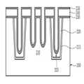
도 1a 내지 도 1e는 본 발명의 실시 예에 따른 반도체 소자 및 그 제조 방법을 도시한 단면도들이다.1A to 1E are cross-sectional views illustrating a semiconductor device and a method of manufacturing the same according to an embodiment of the present invention.
도 1a를 참조하면, 반도체 기판(200)상에 감광막을 형성한 후, 트렌치(Trench) 마스크를 이용한 노광 및 현상 공정으로 감광막 패턴(미도시)을 형성한다. 감광막 패턴을 마스크로 상기 반도체 기판(200)을 식각하여 트렌치(미도시)를 형성한다. 상기 트렌치에 패드 질화막(215) 및 절연막(미도시)을 매립하여 활성 영역(210)을 정의하는 소자분리막(220)을 형성한다.Referring to FIG. 1A, after the photoresist film is formed on the
다음에는, 상기 활성 영역(210) 및 소자분리막(220)을 포함한 전면에 감광막을 형성한 후, 리세스(Recess) 마스크를 이용한 노광 및 현상 공정으로 감광막 패턴(미도시)을 형성한다. 이후, 감광막 패턴을 마스크로 상기 활성 영역(210) 및 소자분리막(220)을 식각하여 리세스(225)를 형성한다.Next, after the photoresist film is formed on the entire surface including the
다음에는, 리세스(225)를 포함한 전면에 게이트 절연막(230) 및 하드마스크층 질화막 패턴(240)을 형성한 후, 상기 리세스(225) 및 상기 하드마스층 질화막 패턴(240)을 포함한 전면에 제 1 게이트 전극 물질(250)을 형성한다. 이때, 제 1 게이트 전극 물질(250)은 TiN, TaN, Ti, Ta, Mo, Al 및 이들의 조합 중 선택 어느 하나의 물질로 형성하는 것이 바람직하다.Next, after the
도 1b를 참조하면, 제 1 게이트 전극 물질(250)을 포함한 전면에 상기 하드마스크층으로 이용하는 폴리실리콘층(260)을 형성한다. 이때, 하드마스크층은 폴리실리콘층(Polysilicon), 산화막(Oxide), 감광막(Photo resist), 탄소막(Carbon) 및 이들의 조합 중 선택된 어느 하나의 층으로 형성 가능하다.Referring to FIG. 1B, a
도 1c를 참조하면, 폴리실리콘층(260) 및 제 1 게이트 전극 물질(250)을 에치백(Etchback)하여 일부를 제거한 후, 상기 폴리실리콘층(260)을 완전히 제거하여 리세스(225) 내의 하부의 일부 영역에만 제 1 게이트 전극 패턴(255)이 남는다. 여기서, 리세스(225) 내의 하부의 일부 영역에만 제 1 게이트 전극 패턴(255)이 남아있기 때문에 후속 공정 시 추가로 게이트 전극 물질(나이트라이드 티타늄층 및 텅스텐층)을 증착하게 되면 게이트 전극의 하부가 상부보다 두껍게 형성되어 워크 펑션(work function) 값을 크게 유지할 수 있다.Referring to FIG. 1C, the
도 1d를 참조하면, 상기 리세스(225)에 제 2 게이트 전극 물질(270, 280)을 증착한다. 이때, 제 2 게이트 전극 물질(270, 280)은 TiN, TaN, Ti, Ta, Mo, Al 및 이들의 조합 중 선택 어느 하나의 물질과 텅스텐(W)으로 형성하는 것이 바람직하다.Referring to FIG. 1D, second
여기서, 게이트 전극 물질(텅스텐)의 상부(A 영역)는 하부(B 영역)보다 더 넓게 형성되어 게이트 전극의 저항을 줄일 수 있다.Here, the upper portion (region A) of the gate electrode material (tungsten) may be formed wider than the lower portion (region B) to reduce the resistance of the gate electrode.
도 1e를 참조하면, 상기 제 2 게이트 전극 물질(270, 280)을 에치백(Etchback)하여 게이트 전극이 서로 분리되는 매립 게이트(Buried Gate, 290)를 완성한다.Referring to FIG. 1E, the second
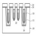
도 2a 내지 도 2d는 본 발명의 다른 실시 예에 따른 반도체 소자 및 그 제조 방법을 도시한 단면도들이다.2A to 2D are cross-sectional views illustrating a semiconductor device and a method of manufacturing the same according to other embodiments of the inventive concept.
도 2a를 참조하면, 반도체 기판(300)상에 감광막을 형성한 후, 트렌치(Trench) 마스크를 이용한 노광 및 현상 공정으로 감광막 패턴(미도시)을 형성한다. 감광막 패턴을 마스크로 상기 반도체 기판(300)을 식각하여 트렌치(미도시)를 형성한다. 상기 트렌치에 패드 질화막(315) 및 절연막(미도시)을 매립하여 활성 영역(310)을 정의하는 소자분리막(320)을 형성한다.Referring to FIG. 2A, after the photoresist film is formed on the
다음에는, 상기 활성 영역(310) 및 소자분리막(320)을 포함한 전면에 감광막을 형성한 후, 리세스(Recess) 마스크를 이용한 노광 및 현상 공정으로 감광막 패턴(미도시)을 형성한다. 이후, 감광막 패턴을 마스크로 상기 활성 영역(310) 및 소자분리막(320)을 식각하여 리세스(325)를 형성한다.Next, after the photoresist film is formed on the entire surface including the
다음에는, 리세스(325)를 포함한 전면에 게이트 절연막(330) 및 하드마스크층 질화막 패턴(340)을 형성한 후, 상기 하드마스층 질화막 패턴(340)을 포함한 전면에 제 1 게이트 전극 물질(350, 360)을 형성한다. 이때, 제 1 게이트 전극 물질(350, 360)은 TiN, TaN, Ti, Ta, Mo, Al 및 이들의 조합 중 선택 어느 하나의 물질과 텅스텐(W)으로 형성하는 것이 바람직하다.Next, after the
도 2b를 참조하면, 상기 하드마스크층 질화막 패턴(340)이 노출될 때까지 제 1 게이트 전극 물질(350, 360)을 에치백(Etchback, 370)하여 제 1 게이트 전극 패턴(355, 365)을 형성한다. 후속 공정 시 게이트 전극 물질(나이트라이드 티타늄층 및 텅스텐층)을 추가 증착하게 되면 게이트 전극(나이트라이드 티타늄층)의 하부는 상기 게이트 전극의 상부에 비해 두텁게 형성되어 워크 펑션(work function)이 큰 상태를 유지하는 장점이 있다.Referring to FIG. 2B, the first
도 2c를 참조하면, 제 1 게이트 전극 패턴(355, 365)을 포함한 전면에 제 2 게이트 전극 물질(380, 390)을 형성한다. 이때, 제 2 게이트 전극 물질(380, 390)은 TiN, TaN, Ti, Ta, Mo, Al 및 이들의 조합 중 선택 어느 하나의 물질과 텅스텐(W)으로 형성하는 것이 바람직하다.Referring to FIG. 2C, second
여기서, 제 2 게이트 전극 물질(텅스텐층, 390)의 상부(A 영역)는 다른 제 1 게이트 전극 물질(텅스텐층, 365)의 하부(B 영역)보다 더 넓게 형성함으로써 게이트 전극의 저항을 줄일 수 있다.Here, the upper portion (region A) of the second gate electrode material (tungsten layer) 390 may be formed wider than the lower portion (region B) of the other first gate electrode material (tungsten layer) 365 to reduce the resistance of the gate electrode. have.
도 2d를 참조하면, 제 2 게이트 전극 물질(380, 390)을 에치백(Etchback, 400)하여 제 2 게이트 전극 패턴(385, 395)으로 형성된 매립 게이트(Buried Gate, 410)를 완성한다.Referring to FIG. 2D, the buried
전술한 바와 같이, 본 발명은 리세스 내의 하부에 형성된 게이트 전극 물질(TiN)을 두껍게 형성하여 워크 펑션(work function)이 높은 상태를 유지하고, 리세스 내의 게이트 전극(W)의 상부를 하부보다 더 넓게 형성함으로써 게이트 전극의 저항을 줄일 수 있는 장점을 가진다.As described above, the present invention forms a thick gate electrode material TiN formed in the lower portion of the recess so that the work function is high, and the upper portion of the gate electrode W in the recess is lower than the lower portion. By forming a wider it has the advantage of reducing the resistance of the gate electrode.
아울러 본 발명의 바람직한 실시 예는 예시의 목적을 위한 것으로, 당업자라면 첨부된 특허청구범위의 기술적 사상과 범위를 통해 다양한 수정, 변경, 대체 및 부가가 가능할 것이며, 이러한 수정 변경 등은 이하의 특허청구범위에 속하는 것으로 보아야 할 것이다.It will be apparent to those skilled in the art that various modifications, additions, and substitutions are possible, and that various modifications, additions and substitutions are possible, within the spirit and scope of the appended claims. As shown in Fig.
Claims (13)
Translated fromKorean상기 리세스를 포함한 전면에 제 1 게이트 전극 물질 및 하드마스크층을 형성하는 단계;
상기 하드마스크층 및 상기 제 1 게이트 전극 물질을 식각하여 상기 리세스의 내측 하부에 상기 제 1 게이트 전극 패턴을 형성하는 단계;
상기 리세스를 포함한 전면에 제 2 게이트 전극 물질을 형성하는 단계; 및
상기 제 2 게이트 전극 물질을 식각하여 상기 제 2 게이트 전극 물질을 분리하는 단계
를 포함하는 반도체 소자의 제조 방법.Forming a recess on the semiconductor substrate;
Forming a first gate electrode material and a hard mask layer on the entire surface including the recess;
Etching the hard mask layer and the first gate electrode material to form the first gate electrode pattern on an inner lower portion of the recess;
Forming a second gate electrode material on the front surface including the recess; And
Etching the second gate electrode material to separate the second gate electrode material
Method for manufacturing a semiconductor device comprising a.
상기 제 1 게이트 전극 물질은 TiN, TaN, Ti, Ta, Mo, Al 및 이들의 조합 중 선택 어느 하나의 물질로 형성하는 것을 특징으로 하는 반도체 소자의 제조 방법.The method of claim 1,
The first gate electrode material is formed of any one selected from TiN, TaN, Ti, Ta, Mo, Al, and a combination thereof.
상기 하드마스크층은 폴리실리콘층, 산화막, 감광막, 탄소층 및 이들의 조합 중 선택된 어느 하나를 이용하는 것을 특징으로 하는 반도체 소자의 제조 방법.The method of claim 1,
The hard mask layer is a method for manufacturing a semiconductor device, characterized in that any one selected from polysilicon layer, oxide film, photosensitive film, carbon layer and combinations thereof.
상기 제 2 게이트 전극 물질은 TiN, TaN, Ti, Ta, Mo, Al 및 이들의 조합 중 선택 어느 하나의 물질과 텅스텐(W)으로 형성하는 것을 특징으로 하는 반도체 소자의 제조 방법.The method of claim 1,
The second gate electrode material is formed of tungsten (W) and any one selected from TiN, TaN, Ti, Ta, Mo, Al, and a combination thereof.
상기 텅스텐(W)층은 리세스 내의 하부보다 상부에 더 넓게 증착되는 것을 특징으로 하는 반도체 소자의 제조 방법.The method of claim 4, wherein
And the tungsten (W) layer is deposited on top of the bottom of the recess in a wider area.
상기 리세스 내의 하부의 상기 제 1 및 제 2 게이트 전극 물질의 두께는 상기 리세스 내의 상부의 상기 제 2 게이트 전극 물질의 두께보다 두껍게 형성되는 것을 특징으로 하는 반도체 소자의 제조 방법.The method of claim 1,
And wherein the thickness of the first and second gate electrode material below the recess is thicker than the thickness of the second gate electrode material above the recess.
상기 제 2 게이트 전극 물질을 분리하는 단계는 에치백(Etchback) 공정을 이용하는 것을 특징으로 하는 반도체 소자의 제조 방법.The method of claim 1,
And separating the second gate electrode material using an etchback process.
상기 리세스를 포함한 전면에 제 1 게이트 전극 물질을 형성하는 단계;
상기 제 1 게이트 전극 물질을 식각하여 상기 리세스의 내측 하부에 상기 제 1 게이트 전극 패턴을 형성하는 단계;
상기 리세스 내에 제 2 게이트 전극 물질을 형성하는 단계; 및
상기 제 2 게이트 전극 물질을 식각하여 상기 리세스 간의 상기 제 2 게이트 전극 물질을 분리하는 단계
를 포함하는 반도체 소자의 제조 방법.Forming a recess on the semiconductor substrate;
Forming a first gate electrode material on the front surface including the recess;
Etching the first gate electrode material to form the first gate electrode pattern under the inner side of the recess;
Forming a second gate electrode material in the recess; And
Etching the second gate electrode material to separate the second gate electrode material between the recesses
Method for manufacturing a semiconductor device comprising a.
상기 제 1 및 제 2 게이트 전극 물질은 TiN, TaN, Ti, Ta, Mo, Al 및 이들의 조합 중 선택된 어느 하나의 물질과 텅스텐(W)으로 형성하는 것을 특징으로 하는 반도체 소자의 제조 방법.The method of claim 8,
The first and second gate electrode materials are formed of tungsten (W) and any one selected from TiN, TaN, Ti, Ta, Mo, Al, and a combination thereof.
상기 제 2 게이트 전극 물질을 분리하는 단계는 에치백(Etchback) 공정을 이용하는 것을 특징으로 하는 반도체 소자의 제조 방법.The method of claim 8,
And separating the second gate electrode material using an etchback process.
Priority Applications (3)
| Application Number | Priority Date | Filing Date | Title |
|---|---|---|---|
| KR1020100006524AKR101110437B1 (en) | 2010-01-25 | 2010-01-25 | Semiconductor Device and Method for Manufacturing the same |
| US12/848,045US8278201B2 (en) | 2010-01-25 | 2010-07-30 | Semiconductor device having a buried gate and method for manufacturing the same |
| US13/597,137US8546858B2 (en) | 2010-01-25 | 2012-08-28 | Semiconductor device and method for manufacturing the same |
Applications Claiming Priority (1)
| Application Number | Priority Date | Filing Date | Title |
|---|---|---|---|
| KR1020100006524AKR101110437B1 (en) | 2010-01-25 | 2010-01-25 | Semiconductor Device and Method for Manufacturing the same |
Publications (2)
| Publication Number | Publication Date |
|---|---|
| KR20110087071A KR20110087071A (en) | 2011-08-02 |
| KR101110437B1true KR101110437B1 (en) | 2012-02-24 |
Family
ID=44308319
Family Applications (1)
| Application Number | Title | Priority Date | Filing Date |
|---|---|---|---|
| KR1020100006524AActiveKR101110437B1 (en) | 2010-01-25 | 2010-01-25 | Semiconductor Device and Method for Manufacturing the same |
Country Status (2)
| Country | Link |
|---|---|
| US (2) | US8278201B2 (en) |
| KR (1) | KR101110437B1 (en) |
Families Citing this family (22)
| Publication number | Priority date | Publication date | Assignee | Title |
|---|---|---|---|---|
| KR102008318B1 (en)* | 2012-12-06 | 2019-08-08 | 삼성전자주식회사 | Semiconductor device |
| KR20150090669A (en)* | 2014-01-29 | 2015-08-06 | 에스케이하이닉스 주식회사 | Dual work function bruied gate type transistor, method for manufacturing the same and electronic device having the same |
| KR20150090674A (en)* | 2014-01-29 | 2015-08-06 | 에스케이하이닉스 주식회사 | Transistor having dual work function bruied gate electrode, method for manufacturing the same and electronic device having the same |
| KR102162733B1 (en)* | 2014-05-29 | 2020-10-07 | 에스케이하이닉스 주식회사 | Dual work function bruied gate type transistor, method for manufacturing the same and electronic device having the same |
| KR102312262B1 (en) | 2014-09-02 | 2021-10-15 | 삼성전자주식회사 | Semiconductor device and method of fabricating the same |
| US9859157B1 (en) | 2016-07-14 | 2018-01-02 | International Business Machines Corporation | Method for forming improved liner layer and semiconductor device including the same |
| KR102616853B1 (en)* | 2016-07-15 | 2023-12-26 | 에스케이하이닉스 주식회사 | 3- Dimensions Semiconductor Integrated Circuit Device And Method of Manufacturing The same |
| KR102429608B1 (en) | 2016-08-17 | 2022-08-04 | 삼성전자주식회사 | Semiconductor device and method for fabricating the same |
| CN108807384B (en)* | 2017-05-04 | 2019-10-18 | 联华电子股份有限公司 | Semiconductor element and manufacturing method thereof |
| KR102279732B1 (en)* | 2017-07-21 | 2021-07-22 | 삼성전자주식회사 | Semiconductor memory device and method of forming the same |
| CN109427652B (en) | 2017-08-31 | 2020-08-18 | 联华电子股份有限公司 | Method for manufacturing embedded character line structure and structure |
| CN109801880B (en) | 2017-11-17 | 2021-05-18 | 联华电子股份有限公司 | Buried character line of dynamic random access memory and method of making the same |
| KR102697920B1 (en)* | 2018-11-26 | 2024-08-22 | 삼성전자주식회사 | Semiconductor device and method of fabricating the same |
| KR20220014588A (en)* | 2020-07-29 | 2022-02-07 | 삼성전자주식회사 | A semiconductor device |
| US11424360B1 (en)* | 2021-02-04 | 2022-08-23 | Nanya Technology Corporation | Semiconductor device and method for manufacturing the same |
| TWI803217B (en)* | 2021-12-16 | 2023-05-21 | 南亞科技股份有限公司 | Memory device having word lines with reduced leakage |
| US20230197771A1 (en)* | 2021-12-16 | 2023-06-22 | Nanya Technology Corporation | Memory device having word lines with reduced leakage |
| TWI794055B (en)* | 2021-12-20 | 2023-02-21 | 南亞科技股份有限公司 | Memory device having word lines with improved resistance and manufacturing method thereof |
| US12262524B2 (en)* | 2021-12-20 | 2025-03-25 | Nanya Technology Corporation | Method of manufacturing memory device having word lines with improved resistance |
| US12414292B2 (en) | 2022-03-16 | 2025-09-09 | Nanya Technology Corporation | Method for manufacturing memory device having word line with dual conductive materials |
| TWI825735B (en)* | 2022-03-16 | 2023-12-11 | 南亞科技股份有限公司 | Memory device having word line with dual conductive materials |
| US20240098978A1 (en)* | 2022-09-21 | 2024-03-21 | Nanya Technology Corporation | Semiconductor device and method for manufacturing the same |
Citations (1)
| Publication number | Priority date | Publication date | Assignee | Title |
|---|---|---|---|---|
| KR20090076028A (en)* | 2008-01-07 | 2009-07-13 | 삼성전자주식회사 | Semiconductor device and manufacturing method |
Family Cites Families (4)
| Publication number | Priority date | Publication date | Assignee | Title |
|---|---|---|---|---|
| US6087222A (en)* | 1998-03-05 | 2000-07-11 | Taiwan Semiconductor Manufacturing Company | Method of manufacture of vertical split gate flash memory device |
| JP2001168092A (en)* | 1999-01-08 | 2001-06-22 | Toshiba Corp | Semiconductor device and method of manufacturing the same |
| KR100614240B1 (en)* | 2004-06-10 | 2006-08-18 | 삼성전자주식회사 | Semiconductor device including field effect transistor and method for forming same |
| US7494876B1 (en)* | 2005-04-21 | 2009-02-24 | Vishay Siliconix | Trench-gated MIS device having thick polysilicon insulation layer at trench bottom and method of fabricating the same |
- 2010
- 2010-01-25KRKR1020100006524Apatent/KR101110437B1/enactiveActive
- 2010-07-30USUS12/848,045patent/US8278201B2/enactiveActive
- 2012
- 2012-08-28USUS13/597,137patent/US8546858B2/enactiveActive
Patent Citations (1)
| Publication number | Priority date | Publication date | Assignee | Title |
|---|---|---|---|---|
| KR20090076028A (en)* | 2008-01-07 | 2009-07-13 | 삼성전자주식회사 | Semiconductor device and manufacturing method |
Also Published As
| Publication number | Publication date |
|---|---|
| US8546858B2 (en) | 2013-10-01 |
| KR20110087071A (en) | 2011-08-02 |
| US8278201B2 (en) | 2012-10-02 |
| US20120319195A1 (en) | 2012-12-20 |
| US20110180868A1 (en) | 2011-07-28 |
Similar Documents
| Publication | Publication Date | Title |
|---|---|---|
| KR101110437B1 (en) | Semiconductor Device and Method for Manufacturing the same | |
| KR101205143B1 (en) | Semiconductor Device and Method for Manufacturing the same | |
| CN102214578B (en) | Semiconductor device and manufacture method thereof | |
| KR101139987B1 (en) | Semiconductor Device and Method for Manufacturing the same | |
| KR101087895B1 (en) | Semiconductor element and manufacturing method thereof | |
| KR101095686B1 (en) | Semiconductor memory device and manufacturing method thereof | |
| KR101194872B1 (en) | Semiconductor memory device | |
| KR101095802B1 (en) | Semiconductor element and manufacturing method thereof | |
| US20150214147A1 (en) | Semiconductor device and method for manufacturing the same | |
| KR101139464B1 (en) | Semiconductor Device and Method for Manufacturing the same | |
| KR101205160B1 (en) | Semiconductor device and method of fabricating the same | |
| KR101095722B1 (en) | Manufacturing Method of Semiconductor Device | |
| KR101185948B1 (en) | Method for Manufacturing Semiconductor Device | |
| KR20120042575A (en) | Method for manufacturing semiconductor device | |
| KR20110101924A (en) | Manufacturing Method of Semiconductor Device | |
| KR20120030873A (en) | Semiconductor device and method for manufacturing the same | |
| KR20120030872A (en) | Method for manufacturing semiconductor device | |
| KR20110132752A (en) | Manufacturing Method of Semiconductor Device |
Legal Events
| Date | Code | Title | Description |
|---|---|---|---|
| A201 | Request for examination | ||
| PA0109 | Patent application | Patent event code:PA01091R01D Comment text:Patent Application Patent event date:20100125 | |
| PA0201 | Request for examination | ||
| E902 | Notification of reason for refusal | ||
| PE0902 | Notice of grounds for rejection | Comment text:Notification of reason for refusal Patent event date:20110513 Patent event code:PE09021S01D | |
| PG1501 | Laying open of application | ||
| E701 | Decision to grant or registration of patent right | ||
| PE0701 | Decision of registration | Patent event code:PE07011S01D Comment text:Decision to Grant Registration Patent event date:20111228 | |
| GRNT | Written decision to grant | ||
| PR0701 | Registration of establishment | Comment text:Registration of Establishment Patent event date:20120119 Patent event code:PR07011E01D | |
| PR1002 | Payment of registration fee | Payment date:20120119 End annual number:3 Start annual number:1 | |
| PG1601 | Publication of registration | ||
| FPAY | Annual fee payment | Payment date:20141218 Year of fee payment:4 | |
| PR1001 | Payment of annual fee | Payment date:20141218 Start annual number:4 End annual number:4 | |
| FPAY | Annual fee payment | Payment date:20151221 Year of fee payment:5 | |
| PR1001 | Payment of annual fee | Payment date:20151221 Start annual number:5 End annual number:5 | |
| FPAY | Annual fee payment | Payment date:20161125 Year of fee payment:6 | |
| PR1001 | Payment of annual fee | Payment date:20161125 Start annual number:6 End annual number:6 | |
| FPAY | Annual fee payment | Payment date:20171220 Year of fee payment:7 | |
| PR1001 | Payment of annual fee | Payment date:20171220 Start annual number:7 End annual number:7 | |
| FPAY | Annual fee payment | Payment date:20181219 Year of fee payment:8 | |
| PR1001 | Payment of annual fee | Payment date:20181219 Start annual number:8 End annual number:8 | |
| FPAY | Annual fee payment | Payment date:20191224 Year of fee payment:9 | |
| PR1001 | Payment of annual fee | Payment date:20191224 Start annual number:9 End annual number:9 | |
| PR1001 | Payment of annual fee | Payment date:20201228 Start annual number:10 End annual number:10 | |
| PR1001 | Payment of annual fee | Payment date:20221227 Start annual number:12 End annual number:12 | |
| PR1001 | Payment of annual fee | Payment date:20231227 Start annual number:13 End annual number:13 | |
| PR1001 | Payment of annual fee | Payment date:20241226 Start annual number:14 End annual number:14 |