KR101101785B1 - Patterning method - Google Patents
Patterning methodDownload PDFInfo
- Publication number
- KR101101785B1 KR101101785B1KR1020117004101AKR20117004101AKR101101785B1KR 101101785 B1KR101101785 B1KR 101101785B1KR 1020117004101 AKR1020117004101 AKR 1020117004101AKR 20117004101 AKR20117004101 AKR 20117004101AKR 101101785 B1KR101101785 B1KR 101101785B1
- Authority
- KR
- South Korea
- Prior art keywords
- film
- forming
- pattern
- gas
- oxygen
- Prior art date
- Legal status (The legal status is an assumption and is not a legal conclusion. Google has not performed a legal analysis and makes no representation as to the accuracy of the status listed.)
- Active
Links
Images


Classifications
- H—ELECTRICITY
- H01—ELECTRIC ELEMENTS
- H01L—SEMICONDUCTOR DEVICES NOT COVERED BY CLASS H10
- H01L21/00—Processes or apparatus adapted for the manufacture or treatment of semiconductor or solid state devices or of parts thereof
- H01L21/02—Manufacture or treatment of semiconductor devices or of parts thereof
- H01L21/027—Making masks on semiconductor bodies for further photolithographic processing not provided for in group H01L21/18 or H01L21/34
- H01L21/0271—Making masks on semiconductor bodies for further photolithographic processing not provided for in group H01L21/18 or H01L21/34 comprising organic layers
- H01L21/0273—Making masks on semiconductor bodies for further photolithographic processing not provided for in group H01L21/18 or H01L21/34 comprising organic layers characterised by the treatment of photoresist layers
- H01L21/0274—Photolithographic processes
- H—ELECTRICITY
- H01—ELECTRIC ELEMENTS
- H01L—SEMICONDUCTOR DEVICES NOT COVERED BY CLASS H10
- H01L21/00—Processes or apparatus adapted for the manufacture or treatment of semiconductor or solid state devices or of parts thereof
- H01L21/02—Manufacture or treatment of semiconductor devices or of parts thereof
- H01L21/027—Making masks on semiconductor bodies for further photolithographic processing not provided for in group H01L21/18 or H01L21/34
- H01L21/0271—Making masks on semiconductor bodies for further photolithographic processing not provided for in group H01L21/18 or H01L21/34 comprising organic layers
- H01L21/0273—Making masks on semiconductor bodies for further photolithographic processing not provided for in group H01L21/18 or H01L21/34 comprising organic layers characterised by the treatment of photoresist layers
- G—PHYSICS
- G03—PHOTOGRAPHY; CINEMATOGRAPHY; ANALOGOUS TECHNIQUES USING WAVES OTHER THAN OPTICAL WAVES; ELECTROGRAPHY; HOLOGRAPHY
- G03F—PHOTOMECHANICAL PRODUCTION OF TEXTURED OR PATTERNED SURFACES, e.g. FOR PRINTING, FOR PROCESSING OF SEMICONDUCTOR DEVICES; MATERIALS THEREFOR; ORIGINALS THEREFOR; APPARATUS SPECIALLY ADAPTED THEREFOR
- G03F7/00—Photomechanical, e.g. photolithographic, production of textured or patterned surfaces, e.g. printing surfaces; Materials therefor, e.g. comprising photoresists; Apparatus specially adapted therefor
- G03F7/26—Processing photosensitive materials; Apparatus therefor
- G03F7/40—Treatment after imagewise removal, e.g. baking
- G03F7/405—Treatment with inorganic or organometallic reagents after imagewise removal
- G—PHYSICS
- G03—PHOTOGRAPHY; CINEMATOGRAPHY; ANALOGOUS TECHNIQUES USING WAVES OTHER THAN OPTICAL WAVES; ELECTROGRAPHY; HOLOGRAPHY
- G03F—PHOTOMECHANICAL PRODUCTION OF TEXTURED OR PATTERNED SURFACES, e.g. FOR PRINTING, FOR PROCESSING OF SEMICONDUCTOR DEVICES; MATERIALS THEREFOR; ORIGINALS THEREFOR; APPARATUS SPECIALLY ADAPTED THEREFOR
- G03F7/00—Photomechanical, e.g. photolithographic, production of textured or patterned surfaces, e.g. printing surfaces; Materials therefor, e.g. comprising photoresists; Apparatus specially adapted therefor
- G03F7/0035—Multiple processes, e.g. applying a further resist layer on an already in a previously step, processed pattern or textured surface
- G—PHYSICS
- G03—PHOTOGRAPHY; CINEMATOGRAPHY; ANALOGOUS TECHNIQUES USING WAVES OTHER THAN OPTICAL WAVES; ELECTROGRAPHY; HOLOGRAPHY
- G03F—PHOTOMECHANICAL PRODUCTION OF TEXTURED OR PATTERNED SURFACES, e.g. FOR PRINTING, FOR PROCESSING OF SEMICONDUCTOR DEVICES; MATERIALS THEREFOR; ORIGINALS THEREFOR; APPARATUS SPECIALLY ADAPTED THEREFOR
- G03F7/00—Photomechanical, e.g. photolithographic, production of textured or patterned surfaces, e.g. printing surfaces; Materials therefor, e.g. comprising photoresists; Apparatus specially adapted therefor
- G03F7/004—Photosensitive materials
- G03F7/075—Silicon-containing compounds
- G03F7/0755—Non-macromolecular compounds containing Si-O, Si-C or Si-N bonds
- H—ELECTRICITY
- H01—ELECTRIC ELEMENTS
- H01L—SEMICONDUCTOR DEVICES NOT COVERED BY CLASS H10
- H01L21/00—Processes or apparatus adapted for the manufacture or treatment of semiconductor or solid state devices or of parts thereof
- H01L21/02—Manufacture or treatment of semiconductor devices or of parts thereof
- H01L21/02104—Forming layers
- H01L21/02107—Forming insulating materials on a substrate
- H01L21/02109—Forming insulating materials on a substrate characterised by the type of layer, e.g. type of material, porous/non-porous, pre-cursors, mixtures or laminates
- H01L21/02112—Forming insulating materials on a substrate characterised by the type of layer, e.g. type of material, porous/non-porous, pre-cursors, mixtures or laminates characterised by the material of the layer
- H01L21/02123—Forming insulating materials on a substrate characterised by the type of layer, e.g. type of material, porous/non-porous, pre-cursors, mixtures or laminates characterised by the material of the layer the material containing silicon
- H01L21/02164—Forming insulating materials on a substrate characterised by the type of layer, e.g. type of material, porous/non-porous, pre-cursors, mixtures or laminates characterised by the material of the layer the material containing silicon the material being a silicon oxide, e.g. SiO2
- H—ELECTRICITY
- H01—ELECTRIC ELEMENTS
- H01L—SEMICONDUCTOR DEVICES NOT COVERED BY CLASS H10
- H01L21/00—Processes or apparatus adapted for the manufacture or treatment of semiconductor or solid state devices or of parts thereof
- H01L21/02—Manufacture or treatment of semiconductor devices or of parts thereof
- H01L21/02104—Forming layers
- H01L21/02107—Forming insulating materials on a substrate
- H01L21/02225—Forming insulating materials on a substrate characterised by the process for the formation of the insulating layer
- H01L21/0226—Forming insulating materials on a substrate characterised by the process for the formation of the insulating layer formation by a deposition process
- H01L21/02263—Forming insulating materials on a substrate characterised by the process for the formation of the insulating layer formation by a deposition process deposition from the gas or vapour phase
- H01L21/02271—Forming insulating materials on a substrate characterised by the process for the formation of the insulating layer formation by a deposition process deposition from the gas or vapour phase deposition by decomposition or reaction of gaseous or vapour phase compounds, i.e. chemical vapour deposition
- H01L21/0228—Forming insulating materials on a substrate characterised by the process for the formation of the insulating layer formation by a deposition process deposition from the gas or vapour phase deposition by decomposition or reaction of gaseous or vapour phase compounds, i.e. chemical vapour deposition deposition by cyclic CVD, e.g. ALD, ALE, pulsed CVD
- H—ELECTRICITY
- H01—ELECTRIC ELEMENTS
- H01L—SEMICONDUCTOR DEVICES NOT COVERED BY CLASS H10
- H01L21/00—Processes or apparatus adapted for the manufacture or treatment of semiconductor or solid state devices or of parts thereof
- H01L21/02—Manufacture or treatment of semiconductor devices or of parts thereof
- H01L21/027—Making masks on semiconductor bodies for further photolithographic processing not provided for in group H01L21/18 or H01L21/34
- H01L21/0271—Making masks on semiconductor bodies for further photolithographic processing not provided for in group H01L21/18 or H01L21/34 comprising organic layers
- H—ELECTRICITY
- H01—ELECTRIC ELEMENTS
- H01L—SEMICONDUCTOR DEVICES NOT COVERED BY CLASS H10
- H01L21/00—Processes or apparatus adapted for the manufacture or treatment of semiconductor or solid state devices or of parts thereof
- H01L21/02—Manufacture or treatment of semiconductor devices or of parts thereof
- H01L21/027—Making masks on semiconductor bodies for further photolithographic processing not provided for in group H01L21/18 or H01L21/34
- H01L21/033—Making masks on semiconductor bodies for further photolithographic processing not provided for in group H01L21/18 or H01L21/34 comprising inorganic layers
- H01L21/0334—Making masks on semiconductor bodies for further photolithographic processing not provided for in group H01L21/18 or H01L21/34 comprising inorganic layers characterised by their size, orientation, disposition, behaviour, shape, in horizontal or vertical plane
- H01L21/0337—Making masks on semiconductor bodies for further photolithographic processing not provided for in group H01L21/18 or H01L21/34 comprising inorganic layers characterised by their size, orientation, disposition, behaviour, shape, in horizontal or vertical plane characterised by the process involved to create the mask, e.g. lift-off masks, sidewalls, or to modify the mask, e.g. pre-treatment, post-treatment
- H—ELECTRICITY
- H01—ELECTRIC ELEMENTS
- H01L—SEMICONDUCTOR DEVICES NOT COVERED BY CLASS H10
- H01L21/00—Processes or apparatus adapted for the manufacture or treatment of semiconductor or solid state devices or of parts thereof
- H01L21/02—Manufacture or treatment of semiconductor devices or of parts thereof
- H01L21/04—Manufacture or treatment of semiconductor devices or of parts thereof the devices having potential barriers, e.g. a PN junction, depletion layer or carrier concentration layer
- H01L21/18—Manufacture or treatment of semiconductor devices or of parts thereof the devices having potential barriers, e.g. a PN junction, depletion layer or carrier concentration layer the devices having semiconductor bodies comprising elements of Group IV of the Periodic Table or AIIIBV compounds with or without impurities, e.g. doping materials
- H01L21/30—Treatment of semiconductor bodies using processes or apparatus not provided for in groups H01L21/20 - H01L21/26
- H01L21/302—Treatment of semiconductor bodies using processes or apparatus not provided for in groups H01L21/20 - H01L21/26 to change their surface-physical characteristics or shape, e.g. etching, polishing, cutting
- H01L21/306—Chemical or electrical treatment, e.g. electrolytic etching
- H01L21/3065—Plasma etching; Reactive-ion etching
- H—ELECTRICITY
- H01—ELECTRIC ELEMENTS
- H01L—SEMICONDUCTOR DEVICES NOT COVERED BY CLASS H10
- H01L21/00—Processes or apparatus adapted for the manufacture or treatment of semiconductor or solid state devices or of parts thereof
- H01L21/02—Manufacture or treatment of semiconductor devices or of parts thereof
- H01L21/04—Manufacture or treatment of semiconductor devices or of parts thereof the devices having potential barriers, e.g. a PN junction, depletion layer or carrier concentration layer
- H01L21/18—Manufacture or treatment of semiconductor devices or of parts thereof the devices having potential barriers, e.g. a PN junction, depletion layer or carrier concentration layer the devices having semiconductor bodies comprising elements of Group IV of the Periodic Table or AIIIBV compounds with or without impurities, e.g. doping materials
- H01L21/30—Treatment of semiconductor bodies using processes or apparatus not provided for in groups H01L21/20 - H01L21/26
- H01L21/31—Treatment of semiconductor bodies using processes or apparatus not provided for in groups H01L21/20 - H01L21/26 to form insulating layers thereon, e.g. for masking or by using photolithographic techniques; After treatment of these layers; Selection of materials for these layers
- H01L21/3105—After-treatment
- H01L21/311—Etching the insulating layers by chemical or physical means
- H01L21/31144—Etching the insulating layers by chemical or physical means using masks
- H—ELECTRICITY
- H01—ELECTRIC ELEMENTS
- H01L—SEMICONDUCTOR DEVICES NOT COVERED BY CLASS H10
- H01L21/00—Processes or apparatus adapted for the manufacture or treatment of semiconductor or solid state devices or of parts thereof
- H01L21/02—Manufacture or treatment of semiconductor devices or of parts thereof
- H01L21/04—Manufacture or treatment of semiconductor devices or of parts thereof the devices having potential barriers, e.g. a PN junction, depletion layer or carrier concentration layer
- H01L21/18—Manufacture or treatment of semiconductor devices or of parts thereof the devices having potential barriers, e.g. a PN junction, depletion layer or carrier concentration layer the devices having semiconductor bodies comprising elements of Group IV of the Periodic Table or AIIIBV compounds with or without impurities, e.g. doping materials
- H01L21/30—Treatment of semiconductor bodies using processes or apparatus not provided for in groups H01L21/20 - H01L21/26
- H01L21/31—Treatment of semiconductor bodies using processes or apparatus not provided for in groups H01L21/20 - H01L21/26 to form insulating layers thereon, e.g. for masking or by using photolithographic techniques; After treatment of these layers; Selection of materials for these layers
- H01L21/3205—Deposition of non-insulating-, e.g. conductive- or resistive-, layers on insulating layers; After-treatment of these layers
- H01L21/321—After treatment
- H01L21/3213—Physical or chemical etching of the layers, e.g. to produce a patterned layer from a pre-deposited extensive layer
- H01L21/32139—Physical or chemical etching of the layers, e.g. to produce a patterned layer from a pre-deposited extensive layer using masks
Landscapes
- Engineering & Computer Science (AREA)
- Physics & Mathematics (AREA)
- General Physics & Mathematics (AREA)
- Condensed Matter Physics & Semiconductors (AREA)
- Manufacturing & Machinery (AREA)
- Computer Hardware Design (AREA)
- Microelectronics & Electronic Packaging (AREA)
- Power Engineering (AREA)
- Chemical & Material Sciences (AREA)
- Inorganic Chemistry (AREA)
- Organic Chemistry (AREA)
- Chemical Kinetics & Catalysis (AREA)
- Plasma & Fusion (AREA)
- Spectroscopy & Molecular Physics (AREA)
- Formation Of Insulating Films (AREA)
- Drying Of Semiconductors (AREA)
- Exposure Of Semiconductors, Excluding Electron Or Ion Beam Exposure (AREA)
- Exposure And Positioning Against Photoresist Photosensitive Materials (AREA)
- Photosensitive Polymer And Photoresist Processing (AREA)
- Chemical Vapour Deposition (AREA)
Abstract
Translated fromKoreanDescription
Translated fromKorean본 발명은, 반도체 프로세스에 이용되고, 노광 장치의 해상 한계 이하의 패턴을 형성하는 패터닝 방법에 관한 것이다.This invention relates to the patterning method used for a semiconductor process and forming the pattern below the resolution limit of an exposure apparatus.
반도체 디바이스의 고집적도화에 따라, 제조 프로세스에 요구되는 배선폭 또는 분리폭은 미세화되고 있다. 일반적으로, 미세 패턴은 포토리소그래피 기술을 이용하여 레지스트 패턴을 형성하고, 해당 레지스트 패턴을 에칭 마스크로 이용하여 하지(下地)의 각종 박막을 에칭함으로써 형성된다.With the higher integration of semiconductor devices, the wiring width or separation width required for the manufacturing process is becoming smaller. Generally, a fine pattern is formed by forming a resist pattern using photolithography technique, and etching various thin films of the base using the resist pattern as an etching mask.
미세 패턴을 형성하기 위해서는 포토리소그래피 기술이 중요하지만, 최근의 반도체 디바이스의 미세화는 포토리소그래피 기술의 해상 한계 이하의 치수를 요구하는 데에까지 이르렀다.Photolithography technology is important for forming fine patterns, but the recent miniaturization of semiconductor devices has come to require dimensions below the resolution limit of photolithography technology.
해상 한계 이하의 패턴을 형성하는 기술은, 예를 들면, 특허 문헌 1에 기재되어 있다.The technique of forming a pattern below a resolution limit is described in
특허 문헌 1은, 제 1 감광막 패턴(이하, 제 1 레지스트 패턴이라고 함)을 형성하고, 해당 제 1 레지스트 패턴을 베이크(bake)한 후, 해당 제 1 레지스트 패턴 상에 산화막을 형성한다. 그 후, 제 1 레지스트 패턴끼리의 중간에 제 2 감광막 패턴(이하, 제 2 레지스트 패턴이라고 함)을 형성하고, 제 1 레지스트 패턴 및 제 2 레지스트 패턴을 에칭 마스크로 이용하여 하지(下地)의 박막을 에칭하여 미세 패턴을 형성한다.
특허 문헌 1에 의하면, 2 개의 노광 마스크를 이용하여 미세 패턴을 형성하므로, 1 개의 노광 마스크를 이용하여 미세 패턴을 형성하는 경우에 비해 2 배 이상의 분해능을 얻을 수 있다. 이 때문에, 해상 한계 이하의 미세 패턴을 형성할 수 있다.According to
또한, 레지스트 패턴 상에 산화막을 형성하는 기술은, 예를 들면, 특허 문헌 2에 기재되어 있다.In addition, the technique of forming an oxide film on a resist pattern is described in
특허 문헌 2는, 해상 한계 이하의 미세 패턴을 형성하는 방법은 기재하고 있지 않으나, 레지스트 패턴 상에 산화막을 형성해 둠으로써, 레지스트 패턴의 박형화 현상을 방지할 수 있고, 형성된 미세 패턴에 스트리에이션(striation) 또는 위글링(wiggling)이 발생하는 것을 방지할 수 있는 기술이 기재되어 있다.
특허 문헌 1 : 일본특허공보 제2757983호Patent Document 1: Japanese Patent Publication No. 2757983
특허 문헌 2 : 일본특허공개공보 2004-80033호Patent Document 2: Japanese Patent Laid-Open No. 2004-80033
특허 문헌 1에 의하면, 해상 한계 이하의 미세 패턴을 형성할 수 있다. 그러나, 미세 패턴의 임계 치수(CD)의 균일성의 요구는 갈수록 점점 커지고 있다. 예를 들면, 제 1 레지스트 패턴 상에 형성하는 산화막의 막 두께 균일성이 양호하지 않으면, 미세 패턴에 대한 양호한 CD 컨트롤이 곤란해진다.According to
특허 문헌 2는, 예를 들면, 그 단락 [0010]에, 레지스트 패턴에 손상이 발생하지 않도록, 산화막은 상온 ~ 400℃의 사이의 온도로 형성하는 것이 바람직하다고 하는 것이 기재되고, 이러한 산화막을 실현하는 방법으로서 원자층 퇴적법(ALD)을 개시하고 있다.
그러나, 특허 문헌 2는, ALD보다 더 저온에서, 또한 균일한 막 두께로 산화막을 형성하는 기술에 대해서는 전혀 개시하고 있지 않다.However,
본 발명은, 해상 한계 이하의 피치를 갖는 미세 패턴의 CD 균일성을, 보다 양호하게 할 수 있는 패터닝 방법을 제공하는 것을 목적으로 한다.An object of this invention is to provide the patterning method which can make CD uniformity of the fine pattern which has a pitch below a resolution limit more favorable.
상기 과제를 해결하기 위하여, 본 발명의 제 1 태양에 따른 패터닝 방법은, 기판 상에 제 1 막을 형성하는 공정과, 제 1 막 상에 제 1 레지스트막을 형성하는 공정과, 제 1 레지스트막을 포토리소그래피에 의하여 소정의 피치를 갖는 제 1 레지스트 패턴으로 가공하는 공정과, 유기 실리콘을 포함하는 제 1 가스와 활성화된 산소종을 포함하는 제 2 가스를 해당 기판으로 교대로 공급하여, 제 1 레지스트 패턴 및 제 1 막 상에 실리콘 산화막을 형성하는 공정과, 실리콘 산화막 상에 제 2 레지스트막을 형성하는 공정과, 제 2 레지스트막을 포토리소그래피에 의하여 소정의 피치를 갖는 제 2 레지스트 패턴으로 가공하는 공정과, 제 1 레지스트 패턴 및 제 2 레지스트 패턴을 마스크로 이용하여 제 1 막을 가공하는 공정을 구비한다.In order to solve the said subject, the patterning method which concerns on the 1st aspect of this invention is a process of forming a 1st film on a board | substrate, a process of forming a 1st resist film on a 1st film, and photolithography a 1st resist film. Process of processing into a first resist pattern having a predetermined pitch, and alternately supplying a first gas containing organic silicon and a second gas containing activated oxygen species to the substrate, thereby providing a first resist pattern and Forming a silicon oxide film on the first film, forming a second resist film on the silicon oxide film, processing the second resist film into a second resist pattern having a predetermined pitch by photolithography, and A process of processing a 1st film using a 1st resist pattern and a 2nd resist pattern as a mask is provided.
또한, 본 발명의 제 2 태양에 따른 패터닝 방법은, 기판 상에 제 1 막을 형성하는 공정과, 제 1 막 상에, 제 1 막과는 다른 재료로 구성되는 하드마스크막을 형성하는 공정과, 하드마스크막 상에 제 1 레지스트막을 형성하는 공정과, 제 1 레지스트막을 포토리소그래피에 의하여 소정의 피치를 갖는 제 1 레지스트 패턴으로 가공하는 공정과, 유기 실리콘을 포함하는 제 1 가스와 활성화된 산소종을 포함하는 제 2 가스를 해당 기판으로 교대로 공급하여, 제 1 레지스트 패턴 및 하드마스크막 상에 실리콘 산화막을 형성하는 공정과, 실리콘 산화막 상에 제 2 레지스트막을 형성하는 공정과, 제 2 레지스트막을 포토리소그래피에 의하여 소정의 피치를 갖는 제 2 레지스트 패턴으로 가공하는 공정과, 제 1 레지스트 패턴 및 제 2 레지스트 패턴을 마스크로 이용하여 하드마스크막을 가공하는 공정과, 가공된 하드마스크막을 마스크로 이용하여 제 1 막을 가공하는 공정을 구비한다.Moreover, the patterning method which concerns on the 2nd aspect of this invention is a process of forming a 1st film | membrane on a board | substrate, the process of forming a hardmask film | membrane which consists of materials different from a 1st film on a 1st film, and hard Forming a first resist film on the mask film, processing the first resist film into a first resist pattern having a predetermined pitch by photolithography, a first gas containing organic silicon, and activated oxygen species Alternately supplying a second gas to the substrate to form a silicon oxide film on the first resist pattern and the hard mask film, forming a second resist film on the silicon oxide film, and a second resist film. Processing into a second resist pattern having a predetermined pitch by lithography, and using the first resist pattern and the second resist pattern as masks A process of processing a hard mask film and a process of processing a 1st film using the processed hard mask film as a mask are provided.
본 발명에 의하면, 해상 한계 이하의 피치를 갖는 미세 패턴의 CD 균일성을 보다 양호하게 할 수 있는 패터닝 방법을 제공할 수 있다.According to this invention, the patterning method which can make CD uniformity of the fine pattern which has a pitch below a resolution limit more favorable can be provided.
도 1은 본 발명의 제 1 실시예에 따른 패터닝 방법을 주요 제조 공정마다 도시한 단면도이다.
도 2는 본 발명의 제 1 실시예에 따른 패터닝 방법을 주요 제조 공정마다 도시한 단면도이다.
도 3은 본 발명의 제 1 실시예에 따른 패터닝 방법을 주요 제조 공정마다 도시한 단면도이다.
도 4는 본 발명의 제 1 실시예에 따른 패터닝 방법을 주요 제조 공정마다 도시한 단면도이다.
도 5는 본 발명의 제 1 실시예에 따른 미세 패턴 형성 방법을 주요 제조 공정마다 도시한 단면도이다.
도 6은 본 발명의 제 1 실시예에 따른 패터닝 방법을 주요 제조 공정마다 도시한 단면도이다.
도 7은 본 발명의 제 1 실시예에 따른 패터닝 방법을 주요 제조 공정마다 도시한 단면도이다.
도 8은 본 발명의 제 1 실시예에 따른 패터닝 방법에 사용되는 성막 장치의 일예를 도시한 종단면도이다.
도 9는 실리콘 산화막(104)을 형성하기 위한 성막 장치의 일예를 도시한 횡단면도이다.
도 10은 실리콘 산화막(104)을 형성하기 위한 성막 방법에서의 가스의 공급 타이밍을 도시한 타이밍 차트이다.
도 11은 실리콘 산화막의 성막 방법을 실시할 때의 반응을 설명하기 위한 모식도이다.
도 12는 O2 가스 플라즈마를 이용하여 성막한 경우와 O3 가스를 이용하여 성막한 경우에서 불순물량을 비교한 도면이다.
도 13은 본 발명의 제 2 실시예에 따른 패터닝 방법의 주요 제조 공정을 도시한 단면도이다.
도 14는 본 발명의 제 2 실시예에 따른 패터닝 방법에 사용되는 성막 장치의 일예를 도시한 종단면도이다.
도 15는 본 발명의 제 3 실시예에 따른 패터닝 방법을 주요 제조 공정마다 도시한 단면도이다.
도 16은 본 발명의 제 3 실시예에 따른 패터닝 방법을 주요 제조 공정마다 도시한 단면도이다.
도 17은 본 발명의 제 3 실시예에 따른 패터닝 방법을 주요 제조 공정마다 도시한 단면도이다.
도 18은 본 발명의 제 3 실시예에 따른 패터닝 방법을 주요 제조 공정마다 도시한 단면도이다.
도 19는 본 발명의 제 3 실시예에 따른 패터닝 방법을 주요 제조 공정마다 도시한 단면도이다.
도 20은 본 발명의 제 3 실시예에 따른 패터닝 방법을 주요 제조 공정마다 도시한 단면도이다.
도 21은 본 발명의 제 3 실시예에 따른 패터닝 방법을 주요 제조 공정마다 도시한 단면도이다.
도 22는 본 발명의 제 3 실시예에 따른 패터닝 방법을 주요 제조 공정마다 도시한 단면도이다.
도 23은 본 발명의 제 3 실시예에 따른 패터닝 방법을 주요 제조 공정마다 도시한 단면도이다.
도 24a는 본 발명의 제 4 실시예에 따른 패터닝 방법을 주요 제조 공정마다 도시한 단면도이다.
*도 24b는 본 발명의 제 4 실시예에 따른 패터닝 방법을 주요 제조 공정마다 도시한 단면도이다.
도 24c는 본 발명의 제 4 실시예에 따른 패터닝 방법을 주요 제조 공정마다 도시한 단면도이다.
도 24d는 본 발명의 제 4 실시예에 따른 패터닝 방법을 주요 제조 공정마다 도시한 단면도이다.
도 24e는 본 발명의 제 4 실시예에 따른 패터닝 방법을 주요 제조 공정마다 도시한 단면도이다.
도 24f는 본 발명의 제 4 실시예에 따른 패터닝 방법을 주요 제조 공정마다 도시한 단면도이다.
도 24g는 본 발명의 제 4 실시예에 따른 패터닝 방법을 주요 제조 공정마다 도시한 단면도이다.
도 24h는 본 발명의 제 4 실시예에 따른 패터닝 방법을 주요 제조 공정마다 도시한 단면도이다.
도 24i는 본 발명의 제 4 실시예에 따른 패터닝 방법을 주요 제조 공정마다 도시한 단면도이다.
도 25a는 제 1 내지 제 3 실시예에 따른 패터닝 방법에 이어서 실시할 수 있는 반도체 장치의 제조 방법을 설명하기 위한 단면도이다.
도 25b는 제 1 내지 제 3 실시예에 따른 패터닝 방법에 이어서 실시할 수 있는 반도체 장치의 제조 방법을 설명하기 위한 단면도이다.
도 26a는 제 1 내지 제 3 실시예에 따른 패터닝 방법에 이어서 실시할 수 있는 반도체 장치의 제조 방법을 설명하기 위한 단면도이다.
도 26b는 제 1 내지 제 3 실시예에 따른 패터닝 방법에 이어서 실시할 수 있는 반도체 장치의 제조 방법을 설명하기 위한 단면도이다.
도 27은 제 1 내지 제 3 실시예에 따른 패터닝 방법을 이용하여 제조할 수 있는 반도체 장치의 일예를 도시한 단면도이다.1 is a cross-sectional view showing a patterning method according to a first embodiment of the present invention for each major manufacturing process.
2 is a cross-sectional view showing the patterning method according to the first embodiment of the present invention for each major manufacturing process.
3 is a cross-sectional view showing the patterning method according to the first embodiment of the present invention for each major manufacturing process.
4 is a cross-sectional view showing the patterning method according to the first embodiment of the present invention for each major manufacturing process.
FIG. 5 is a cross-sectional view illustrating a method for forming a fine pattern according to a first embodiment of the present invention for each major manufacturing process. FIG.
6 is a cross-sectional view showing the patterning method according to the first embodiment of the present invention for each major manufacturing process.
7 is a cross-sectional view showing the patterning method according to the first embodiment of the present invention for each major manufacturing process.
8 is a longitudinal sectional view showing an example of a film forming apparatus used in the patterning method according to the first embodiment of the present invention.
9 is a cross-sectional view showing an example of a film forming apparatus for forming the
10 is a timing chart showing a timing of supply of gas in the film forming method for forming the
It is a schematic diagram for demonstrating reaction at the time of performing the film-forming method of a silicon oxide film.
FIG. 12 is a view comparing impurity amounts in the case of film formation using O2 gas plasma and in the case of film formation using O3 gas.
13 is a cross-sectional view showing the main manufacturing process of the patterning method according to the second embodiment of the present invention.
14 is a longitudinal sectional view showing an example of a film forming apparatus used in the patterning method according to the second embodiment of the present invention.
15 is a cross-sectional view showing the patterning method according to the third embodiment of the present invention for each major manufacturing process.
16 is a cross-sectional view showing the patterning method according to the third embodiment of the present invention for each major manufacturing process.
17 is a cross-sectional view showing the patterning method according to the third embodiment of the present invention for each major manufacturing process.
18 is a cross-sectional view showing the patterning method according to the third embodiment of the present invention for each major manufacturing process.
19 is a cross-sectional view showing the patterning method according to the third embodiment of the present invention for each major manufacturing process.
20 is a cross-sectional view showing the patterning method according to the third embodiment of the present invention for each major manufacturing process.
21 is a cross-sectional view showing the patterning method according to the third embodiment of the present invention for each major manufacturing process.
22 is a cross-sectional view showing the patterning method according to the third embodiment of the present invention for each major manufacturing process.
23 is a cross-sectional view showing the patterning method according to the third embodiment of the present invention for each major manufacturing process.
24A is a cross-sectional view showing the patterning method according to the fourth embodiment of the present invention for each major manufacturing process.
24B is a sectional view showing the patterning method according to the fourth embodiment of the present invention for each major manufacturing process.
24C is a cross-sectional view showing the patterning method according to the fourth embodiment of the present invention for each major manufacturing process.
24D is a cross-sectional view showing the patterning method according to the fourth embodiment of the present invention for each major manufacturing process.
24E is a cross-sectional view showing the patterning method according to the fourth embodiment of the present invention for each major manufacturing process.
24F is a cross-sectional view showing the patterning method according to the fourth embodiment of the present invention for each major manufacturing process.
24G is a sectional view showing the patterning method according to the fourth embodiment of the present invention for each major manufacturing process.
24H is a cross-sectional view showing the patterning method according to the fourth embodiment of the present invention for each major manufacturing process.
24I is a sectional view showing the patterning method according to the fourth embodiment of the present invention for each major manufacturing process.
25A is a cross-sectional view for illustrating a method of manufacturing a semiconductor device that can be performed following the patterning method according to the first to third embodiments.
25B is a cross-sectional view for illustrating a method for manufacturing a semiconductor device that can be performed following the patterning method according to the first to third embodiments.
26A is a cross-sectional view for illustrating a method for manufacturing a semiconductor device that can be performed following the patterning method according to the first to third embodiments.
FIG. 26B is a cross-sectional view for illustrating a method for manufacturing a semiconductor device that can be performed following the patterning method according to the first to third embodiments. FIG.
27 is a cross-sectional view illustrating one example of a semiconductor device that can be manufactured using the patterning method according to the first to third embodiments.
이하, 첨부 도면을 참조하여 본 발명의 실시예에 대하여 구체적으로 설명한다.Hereinafter, embodiments of the present invention will be described in detail with reference to the accompanying drawings.
(제 1 실시예)(First embodiment)
도 1 내지 도 7은, 본 발명의 제 1 실시예에 따른 패터닝 방법을 주요 제조 공정마다 도시한 단면도이다.1 to 7 are cross-sectional views showing the patterning method according to the first embodiment of the present invention for each major manufacturing step.
제 1 실시예는, 본 발명에 따른 패터닝 방법의 기본적인 프로세스 순서를 예시하는 것이다.The first embodiment illustrates the basic process sequence of the patterning method according to the present invention.
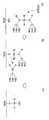
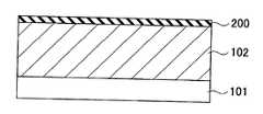
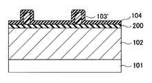
우선, 도 1에 도시한 바와 같이, 반도체 기판(101) 상에 박막(102)을 형성한다. 본 명세서에서는, 반도체 기판(101)은, 반도체, 예를 들면 실리콘 기판만을 도시한 것이 아니라, 반도체 기판 내 또는 반도체 기판 상에 형성된 반도체 소자 또는 집적 회로 패턴에 대응한 도전막, 이들을 절연하는 층간 절연막이 형성된 구조체를 포함한다. 박막(102)은 후에 미세 패턴으로 가공되는 막이며, SiN 또는 SiO2의 절연막이어도 좋고 도전성 폴리실리콘과 같은 도전막이어도 좋다. 본 실시예에서는, 일예로서 박막(102)을 SiN으로 한다. 이어서, 박막(102) 상에 반사 방지 재료를 도포하고, 반사 방지막(BARC)(200)을 형성한다.First, as shown in FIG. 1, the
이어서, 도 2에 도시한 바와 같이, 반사 방지막(200) 상에 포토레지스트를 도포하고, 포토레지스트막을 형성한다. 이어서, 포토리소그래피 기술을 이용하여, 포토레지스트막을 소정의 피치(p1)를 갖는 레지스트 패턴(103)으로 가공한다. 본 실시예에서는, 레지스트 패턴(103)은 라인·앤드·스페이스(line-and-space) 패턴을 가지고, 소정의 피치(p1)는 노광 장치의 해상 한계 정도로 한다.Next, as shown in FIG. 2, a photoresist is apply | coated on the
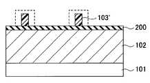
이어서, 도 3에 도시한 바와 같이, 레지스트 패턴(103)을 트리밍하고, 트리밍된 레지스트 패턴(103’)을 얻는다(본 명세서에서는, 제 1 회 트리밍 처리라고 함). 트리밍 처리는, 예를 들면 산소 래디컬 또는 오존 가스를 포함하는 분위기 중에서 실온 ~ 100℃의 온도에서 행해진다.3, the resist
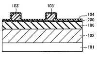
이어서, 도 4에 도시한 바와 같이, 트리밍된 레지스트 패턴(103’) 및 반사 방지막(200) 상에, 박막(102), 반사 방지막(200) 및 레지스트 패턴(103’)과는 다른 실리콘 산화막(104)을 형성한다. 실리콘 산화막(104)은, 후에 행해지는 2 회째의 포토리소그래피 공정으로부터 레지스트 패턴(103’)을 보호하기 위하여 형성된다. 본 명세서에서는, 이러한 실리콘 산화막(104)의 형성을 하드닝 처리라고 한다. 본 실시예에서는, 하드닝 처리를, 유기 실리콘을 포함하는 소스 가스와 플라즈마에 의하여 활성화(여기)된, 산소 래디컬 등의 산소종을 포함하는 가스를 교대로 공급하면서, 트리밍된 레지스트 패턴(103’) 및 반사 방지막(200) 상에 실리콘 산화막(104)을 형성한다.Next, as shown in FIG. 4, on the trimmed resist
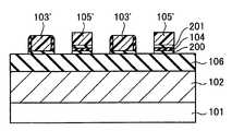
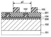
이어서, 도 5에 도시한 바와 같이, 실리콘 산화막(104) 상에 포토레지스트를 도포하고, 포토레지스트막을 형성한다. 이어서, 포토리소그래피 기술을 이용하여, 포토레지스트막을 소정의 피치(p2)를 갖는 레지스트 패턴(105)으로 가공한다. 본 실시예에서는, 레지스트 패턴(105)은 트리밍된 레지스트 패턴(103’)과 마찬가지로, 라인·앤드·스페이스 패턴을 가지고 있다. 또한, 레지스트 패턴(105)의 소정의 피치(p2)는 노광 장치의 해상 한계 정도로 한다. 또한, 본 실시예의 레지스트 패턴(105)은 트리밍된 레지스트 패턴(103’) 사이에 배치되고, 레지스트 패턴(103’)과 레지스트 패턴(105)이 교대로 배치된다.Next, as shown in FIG. 5, a photoresist is applied on the
이어서, 도 6에 도시한 바와 같이, 레지스트 패턴(105)을 트리밍하고, 트리밍된 레지스트 패턴(105’)을 얻는다(본 명세서에서는 제 2 회 트리밍 처리라고 함). 트리밍 처리는, 예를 들어, 산소 래디컬 또는 오존 가스를 포함하는 분위기 중에서, 실온 ~ 100℃의 온도에서 행해질 수 있다. 제 2 회 트리밍 처리에 의하여, 레지스트 패턴(103’ 및 105’)으로 이루어진 레지스트 패턴이 형성된다. 이 레지스트 패턴은, 패턴(103’ 및 105’)이 교대로 배치된 패턴이므로, 그 피치(p3)는 피치(p1 및 p2)보다 좁은 피치, 본 실시예에서는 피치(p1 및 p2)의 거의 1/2의 피치가 된다. 이와 같이, 따로따로 형성된 레지스트 패턴(103’ 및 105’)을 교대로 배치함으로써, 해상 한계 이하의 피치를 갖는 레지스트 패턴을 형성할 수 있다.6, the resist
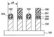
이어서, 도 7에 도시한 바와 같이, 레지스트 패턴(103’ 및 105’)을 에칭 마스크로 이용하여, 반사 방지막(200), 실리콘 산화막(104) 및 박막(102)을 에칭하고, 박막(102)을 원하는 미세 패턴으로 가공한다. 가공된 박막(102)의 피치(p4)는 레지스트 패턴(103’ 및 105’)의 피치(p3)와 거의 동일해지므로, 박막(102)으로 이루어진 미세 패턴의 피치(p4)는 해상 한계 이하로 할 수 있다. 이와 같이 하여, 제 1 실시예에서는 해상 한계 이하의 피치를 갖는 미세 패턴을 형성할 수 있다.Next, as shown in FIG. 7, the
또한, 제 1 실시예에서는 하드닝 처리 시, 유기 실리콘을 포함하는 소스 가스와, 플라즈마에 의하여 여기된 산소 래디컬 등의 산소종을 포함하는 가스를 교대로 공급하여, 반사 방지막(200) 및 트리밍된 레지스트 패턴(103’) 상에 실리콘 산화막(104)을 형성함으로써, 해상 한계 이하의 피치를 갖는 미세 패턴의 CD 균일성을 보다 양호하게 할 수 있다. 이 성막에 대하여 이하 자세하게 설명한다.In addition, in the first embodiment, during the hardening process, a source gas containing organic silicon and a gas containing oxygen species such as oxygen radicals excited by plasma are alternately supplied to prevent the
도 8은 실리콘 산화막(104)의 성막에 사용되는 성막 장치의 일예를 도시한 종단면도, 도 9는 도 8의 성막 장치를 도시한 횡단면도, 도 10은 본 실시예에서의 가스의 공급 타이밍을 도시한 타이밍 차트이다. 또한, 도 9에서는 가열 장치를 생략하고 있다.FIG. 8 is a longitudinal sectional view showing an example of a film forming apparatus used for forming a
도 8 및 도 9에 도시한 바와 같이, 성막 장치(80)는 하단이 개구된 천장이 있는 원통체 형상의 처리 용기(1)를 가지고 있다. 이 처리 용기(1)의 전체는, 예를 들면 석영에 의하여 형성되어 있고, 이 처리 용기(1) 내의 천장에는 석영제의 천정판(2)이 설치되어 봉지되어 있다. 또한, 이 처리 용기(1)의 하단 개구부에는, 예를 들면 스테인레스 스틸에 의하여 원통체 형상으로 성형된 매니폴드(3)가 O 링 등의 씰 부재(4)를 거쳐 연결되어 있다.As shown in FIG. 8 and FIG. 9, the film-forming
상기 매니폴드(3)는, 처리 용기(1)의 하단을 지지하고 있으며, 이 매니폴드(3)의 하방으로부터 피처리체로서 다수 매, 예를 들면 50 ~ 100 매의 반도체 웨이퍼(W)를 다단으로 재치할 수 있는 석영제의 웨이퍼 보트(5)가 처리 용기(1) 내에 삽입할 수 있게 되어 있다. 이 웨이퍼 보트(5)는 3 개의 지지 기둥(6)을 갖고(도 9 참조), 지지 기둥(6)에 형성된 홈에 의해 다수 매의 웨이퍼(W)가 지지되도록 되어 있다.The
이 웨이퍼 보트(5)는 석영제의 보온통(7) 상에 재치되어 있으며, 보온통(7)은 테이블(8) 상에 재치되어 있다. 테이블(8)은 매니폴드(3)의 하단 개구부를 개폐하는, 예를 들면 스테인레스 스틸제의 덮개부(9)를 관통하는 회전축(10) 상에 지지된다.The
그리고, 이 회전축(10)의 관통부에는, 예를 들면 자성 유체 씰(11)이 설치되어 있으며, 회전축(10)을 기밀하게 씰링하면서 회전 가능하게 지지하고 있다. 또한, 덮개부(9)의 주변부와 매니폴드(3)의 하단부와의 사이에는, 예를 들면, O 링으로 이루어지는 씰 부재(12)가 개재되어 있으며, 이에 의해 처리 용기(1) 내의 씰성을 유지하고 있다.And the
상기의 회전축(10)은, 예를 들면 보트 엘리베이터 등의 승강 기구(도시하지 않음)에 지지된 암(13)의 선단에 설치되어 있으며, 웨이퍼 보트(5) 및 덮개부(9) 등은 일체적으로 상승되어 처리 용기(1) 내에 삽입되고, 강하되어 처리 용기(1)로부터 취출된다. 또한, 상기 테이블(8)을 상기 덮개부(9) 측에 고정하여 설치하고, 웨이퍼 보트(5)를 회전시키지 않고 웨이퍼(W)의 처리를 행하여도 좋다.The
또한, 성막 장치(80)는, 처리 용기(1) 내에 산소 함유 가스, 예를 들면 O2 가스를 공급하는 산소 함유 가스 공급 기구(14)와, 처리 용기(1) 내에 Si 소스 가스를 공급하는 Si 소스 가스 공급 기구(15)와, 처리 용기(1) 내에 퍼지 가스로서 불활성 가스, 예를 들면 N2 가스를 공급하는 퍼지 가스 공급 기구(16)를 가지고 있다.Further, the
본 실시예에서는, 실리콘 산화막(104)을 성막하기 위한 Si 소스 가스로서 유기 실리콘을 포함하는 Si 소스 가스를 이용한다. 유기 실리콘을 포함하는 Si 소스 가스의 예는, 아미노실란계 프리커서이다. 아미노실란계 프리커서의 예는, 1 가 또는 2 가의 아미노실란계 프리커서이다. 1 가 또는 2 가의 아미노실란계 프리커서의 구체적인 예는, BTBAS(비스터셔리부틸아미노실란), BDMAS(비스디메틸아미노실란), BDEAS(비스디에틸아미노실란), DMAS(디메틸아미노실란), DEAS(디에틸아미노실란), DPAS(디프로필아미노실란), BAS(부틸아미노실란), DIPAS(디이소프로필아미노실란) 및 BEMAS(비스에틸메틸아미노실란)이다. 또한, 유기 실리콘을 포함하는 Si 소스 가스로서, 상기 열거한 프리커서 중 하나를 이용하여도 좋고, 이들 중 둘 이상을 조합하여 이용해도 좋다.In this embodiment, Si source gas containing organic silicon is used as the Si source gas for forming the
또한, 아미노실란계 프리커서로서는, 3 가의 아미노실란계 프리커서를 이용할 수도 있다. 3 가의 아미노실란계 프리커서의 예는, TDMAS(트리디메틸아미노실란)이다.As the aminosilane-based precursor, a trivalent aminosilane-based precursor can also be used. An example of a trivalent aminosilane-based precursor is TDMAS (tridimethylaminosilane).
또한, 유기 실리콘을 포함하는 Si 소스 가스로서는, 아미노실란계 프리커서 외에, 에톡시실란계 프리커서를 이용할 수도 있다. 에톡시실란계 프리커서의 예는, 예를 들면 TEOS(테트라에톡시실란)이다.As the Si source gas containing organic silicon, in addition to the aminosilane precursor, an ethoxysilane precursor may be used. An example of an ethoxysilane precursor is TEOS (tetraethoxysilane), for example.
산소 함유 가스 공급 기구(14)는, 산소 함유 가스 공급원(17)과, 산소 함유 가스 공급원(17)으로부터 산소 함유 가스를 유도하는 산소 함유 가스 배관(18)과, 이 산소 함유 가스 배관(18)에 접속되고, 매니폴드(3)의 측벽을 내측으로 관통하여 상방향으로 굴곡되어 수직으로 연장되는 석영관으로 이루어지는 산소 함유 가스 분산 노즐(19)을 가지고 있다. 이 산소 함유 가스 분산 노즐(19)의 수직 부분에는, 복수의 가스 토출 홀(19a)이 소정의 간격을 두고 형성되어 있으며, 각 가스 토출 홀(19a)로부터 수평 방향으로 처리 용기(1)를 향하여 대략 균일하게 산소 함유 가스, 예를 들면 O2 가스를 토출할 수 있도록 되어 있다.The oxygen-containing
또한, Si 소스 가스 공급 기구(15)는, Si 소스 가스 공급원(20)과, 이 Si 소스 가스 공급원(20)으로부터 Si 소스 가스를 유도하는 Si 소스 가스 배관(21)과, 이 Si 소스 가스 배관(21)에 접속되고, 매니폴드(3)의 측벽을 내측으로 관통하여 상방향으로 굴곡되어 수직으로 연장되는 석영관으로 이루어지는 Si 소스 가스 분산 노즐(22)을 가지고 있다. 여기에서는 Si 소스 가스 분산 노즐(22)은 2 개 설치되어 있으며(도 9 참조), 각 Si 소스 가스 분산 노즐(22)에는 그 길이 방향을 따라 복수의 가스 토출 홀(22a)이 소정의 간격을 두고 형성되어 있으며, 각 가스 토출 홀(22a)로부터 수평 방향으로 처리 용기(1) 내에 대략 균일하게 유기 실리콘을 포함하는 Si 소스 가스를 토출할 수 있도록 되어 있다. 또한, Si 소스 가스 분산 노즐(22)은 1 개뿐이어도 좋다.The Si source
또한, 퍼지 가스 공급 기구(16)는, 퍼지 가스 공급원(23)과, 퍼지 가스 공급원(23)으로부터 퍼지 가스를 유도하는 퍼지 가스 배관(24)과, 이 퍼지 가스 배관(24)에 접속되고, 매니폴드(3)의 측벽을 관통하여 설치된 퍼지 가스 노즐(25)을 가지고 있다. 퍼지 가스로서는, 불활성 가스, 예를 들면 N2 가스를 적합하게 이용할 수 있다.In addition, the purge
산소 함유 가스 배관(18), Si 소스 가스 배관(21), 퍼지 가스 배관(24)에는 각각 개폐 밸브(18a, 21a, 24a) 및 매스플로우 콘트롤러와 같은 유량 제어기(18b, 21b, 24b)가 설치되어 있으며, 산소 함유 가스, Si 소스 가스 및 퍼지 가스를 각각 유량 제어하면서 공급할 수 있다.In the oxygen-containing
이 플라즈마 생성 기구(30)는 플라즈마 구획벽(32)을 갖고 있다. 플라즈마 구획벽(32)은, 처리 용기(1)의 측벽에서의 소정의 폭을 가진 세로로 긴 부분을 제거함으로써, 형성된 가늘고 긴 개구(31)를 외측으로부터 감싸듯이 처리 용기(1)의 외벽에 기밀하게 장착되어 있다. 또한, 플라즈마 구획벽(32)은, 단면 오목부 형상을 이루어 상하로 가늘고 길게 형성되고, 예를 들면 석영으로 형성되어 있다. 또한, 플라즈마 생성 기구(30)는, 이 플라즈마 구획벽(32)의 양측벽의 외면에 상하 방향을 따라 서로 대향하듯이 배치된 가늘고 긴 한 쌍의 플라즈마 전극(33)과, 이 플라즈마 전극(33)에 급전 라인(34)을 거쳐 접속되어 고주파 전력을 공급하는 고주파 전원(35)을 가지고 있다. 그리고, 상기 플라즈마 전극(33)에 고주파 전원(35)으로부터, 예를 들면 13.56 MHz의 고주파 전압을 인가함으로써, 산소 함유 가스의 플라즈마가 발생할 수 있다. 또한, 이 고주파 전압의 주파수는 13.56 MHz에 한정되지 않고, 다른 주파수, 예를 들면 400 kHz 등을 이용하여도 좋다.This
상기와 같은 플라즈마 구획벽(32)을 형성함으로써, 처리 용기(1)의 측벽의 일부가 오목부 형상으로 외측으로 함몰되고, 플라즈마 구획벽(32)의 내부 공간이 처리 용기(1)의 내부 공간에 일체적으로 연통된다. 또한, 개구(31)는 웨이퍼 보트(5)에서의 웨이퍼(W)가 유지되는 영역의 세로 방향의 전체에 대응하는 높이를 가지고 있다.By forming the
상기 산소 함유 가스 분산 노즐(19)은, 처리 용기(1) 내를 상방향으로 연장되어 가는 도중에, 처리 용기(1)의 반경 방향의 바깥 방향으로 굴곡되고, 상기 플라즈마 구획벽(32) 내의 가장 안쪽 부분(처리 용기(1)의 중심으로부터 가장 멀리 떨어진 부분)을 따라, 상방을 향하여 기립되어 있다. 이 때문에, 가스 토출 홀(19a)로부터 토출된 산소 함유 가스는, 고주파 전원(35)이 온(on) 되어 전극(33) 사이에 생성되는 고주파 전자계에 의하여 플라즈마화되어, 처리 용기(1)의 내부 공간으로 유입된다.The oxygen-containing
플라즈마 구획벽(32)의 외측에는, 이를 감싸도록, 예를 들면 석영으로 이루어지는 절연 보호 커버(36)가 장착되어 있다. 또한, 이 절연 보호 커버(36)의 내측 부분에는, 도시하지 않은 냉매 통로가 설치되어 있으며, 예를 들면, 냉각된 질소 가스를 흐르게 함으로써 상기 플라즈마 전극(33)을 냉각할 수 있다.On the outer side of the
2 개의 Si 소스 가스 분산 노즐(22)은, 처리 용기(1) 내에서 개구(31)의 양측에 위치하도록 기립하고 있으며, 이 Si 소스 가스 분산 노즐(22)에 형성된 복수의 가스 분사 홀(22a)로부터 처리 용기(1)의 내측을 향하여 Si 소스 가스로서 1 분자 내에 1 개 또는 2 개의 아미노기를 갖는 아미노실란 가스를 토출할 수 있도록 되어 있다.The two Si source
한편, 처리 용기(1)의 개구(31)의 반대측에는, 처리 용기(1) 내를 진공 배기하기 위한 배기구(37)가 설치되어 있다. 이 배기구(37)는 처리 용기(1)의 측벽의 일부를 세로로 길게 제거함으로써 형성되어 있다. 처리 용기(1)의 이 배기구(37)에 대응하는 부분에는, 배기구(37)를 감싸도록 단면 오목부 형상으로 성형된 배기구 커버 부재(38)가 용접에 의하여 설치되어 있다. 이 배기구 커버 부재(38)는, 처리 용기(1)의 측벽을 따라 상방으로 연장되어 있으며, 처리 용기(1)의 상방에 가스 출구(39)를 규정하고 있다. 그리고, 이 가스 출구(39)로부터, 도시하지 않은 진공 펌프 등을 포함하는 진공 배기 기구에 의하여 진공 배기된다. 그리고, 이 처리 용기(1)의 외주를 둘러싸듯이, 이 처리 용기(1) 및 그 내부의 웨이퍼(W)를 가열하는 통체 형상의 가열 장치(40)가 설치되어 있다.On the other hand, an
성막 장치(80)의 각 구성부의 제어, 예를 들면 밸브(18a, 21a, 24a)의 개폐에 의한 각 가스의 공급·정지, 매스플로우 콘트롤러(18b, 21b, 24b)에 의한 가스 유량의 제어, 및 고주파 전원(35)의 온·오프 제어, 가열 장치(40)의 제어 등은, 예를 들면 마이크로 프로세서(컴퓨터)로 이루어진 콘트롤러(50)에 의하여 행해진다. 콘트롤러(50)에는, 공정 관리자가 성막 장치(80)를 관리하기 위하여 커맨드의 입력 조작 등을 행하는 키보드 또는 성막 장치(80)의 가동 상황을 표시하는 디스플레이 등으로 이루어진 유저 인터페이스(51)가 접속되어 있다.Control of each component of the
또한, 콘트롤러(50)에는, 성막 장치(80)에서 실행되는 각종 처리를 콘트롤러(50)의 제어로 실현하기 위한 제어 프로그램, 또는 처리 조건에 따라 성막 장치(80)의 각 구성부에 처리를 실행시키기 위한 프로그램, 즉, 레시피가 저장된 기억부(52)가 접속되어 있다. 제어 프로그램 또는 레시피는, 기억 매체(52a)에 기억되어 있어도 좋고, 기억 매체(52a)로부터 기억부(52)에 저장된다. 기억 매체(52a)는 하드 디스크 또는 반도체 메모리여도 좋고, CD-ROM, DVD, 플래시 메모리 등의 가반성(可搬性)의 것이어도 좋다. 또한, 제어 프로그램 또는 레시피는, 다른 장치로부터, 예를 들면 전용 회선을 거쳐 다운로드되어 기억부(52)에 기억되게 해도 좋다.In addition, the
그리고, 필요에 따라, 유저 인터페이스(51)로부터의 지시 등으로, 임의의 레시피를 기억부(52)로부터 독출(讀出)하여 콘트롤러(50)에 실행시킴으로써, 콘트롤러(50)의 제어 하에서 성막 장치(80)에서의 원하는 처리가 행해진다.Then, if necessary, an arbitrary recipe is read out from the
이어서, 이상과 같이 구성된 성막 장치를 이용하여 행해지는 실리콘 산화막(104)의 성막 방법의 일예를, 도 10을 참조하여 설명한다.Next, an example of the film-forming method of the
예를 들면 50 ~ 100 매의 웨이퍼(W)가 탑재된 상태의 웨이퍼 보트(5)를 사전에 소정의 온도로 제어된 처리 용기(1) 내로 그 하방으로부터 상승시킴으로써 로드하고, 덮개부(9)에서 매니폴드(3)의 하단 개구부를 닫음으로써 처리 용기(1) 내를 밀폐 공간으로 한다. 웨이퍼(W)는, 예를 들면 직경 300 mm를 갖고 있어도 좋다.For example, the
그리고, 처리 용기(1) 내를 소정의 프로세스 압력으로 유지하고, 또한 가열 장치(40)로의 공급 전력을 제어하여, 웨이퍼 온도를 상승시켜 프로세스 온도로 유지하고, 웨이퍼 보트(5)를 회전시킨 상태에서 성막 처리를 개시한다.Then, the inside of the
이 때의 성막 처리의 일예를 도 10에 도시한다. 본 일예는, 유기 실리콘을 포함하는 Si 소스 가스로서, 아미노실란 가스, 예를 들면, BTBAS를 이용한 경우이지만, 다른 아미노실란 가스를 이용한 경우 및 에톡시실란 가스를 이용한 경 에도 마찬가지로 실시할 수 있다.An example of the film-forming process at this time is shown in FIG. This example is a case where an aminosilane gas, for example, BTBAS is used as the Si source gas containing organic silicon, but can also be carried out similarly when using another aminosilane gas and when using an ethoxysilane gas.
도 10에 도시한 바와 같이, 성막 처리의 일예에서는, 유기 실리콘을 포함하는 Si 소스 가스를 처리 용기(1) 내로 흘려 Si 소스를 흡착시키는 공정(S1)과, 산소 함유 가스를 플라즈마로 여기함으로써 형성된, 산소 래디컬 등의 산소종을 포함하는 가스를 처리 용기(1)에 공급하여, Si 소스 가스를 산화시키는 공정(S2)을 교대로 반복한다. 또한, 본 일예에서는, 이들 공정(S1)과 공정(S2)과의 사이에서 처리 용기(1) 내로부터 처리 용기(1) 내로 잔류하는 가스를 배출하는 공정(S3)을 실시한다.As shown in FIG. 10, in one example of the film forming process, a step (S1) of flowing a Si source gas containing organic silicon into the
구체적으로는, 본 일예에서는, 공정(S1)에서, Si 소스 가스 공급 기구(15)의 Si 소스 가스 공급원(20)으로부터, Si 소스 가스로서 1 분자 내에 2 개의 아미노기를 갖는 아미노실란 가스, 예를 들면 BTBAS를 Si 소스 가스 배관(21) 및 Si 소스 가스 분산 노즐(22)을 거쳐, 가스 토출 홀(22a)로부터 처리 용기(1) 내로 T1 기간 공급한다. 이에 의해, 웨이퍼(W)에 Si 소스를 흡착시킨다. 이 때의 기간 T1은, 1 ~ 60 sec가 예시된다. 또한, Si 소스 가스의 유량은 10 ~ 500 mL/min(sccm)가 예시된다. 또한, 이 때의 처리 용기(1) 내의 압력은 13.3 ~ 665 Pa가 예시된다.Specifically, in the present example, an aminosilane gas having two amino groups in one molecule as the Si source gas from the Si source
플라즈마에 의하여 생성된, 산소 래디컬 등의 산소종을 포함하는 가스를 공급하는 공정(S2)에서는, 산소 함유 가스 기구(14)의 산소 함유 가스 공급원(17)으로부터, 산소 함유 가스로서, 예를 들면 O2 가스를 산소 함유 가스 배관(18) 및 산소 함유 가스 분산 노즐(19)을 거쳐 가스 토출 홀(19a)로부터 토출하고, 이 때, 플라즈마 생성 기구(30)의 고주파 전원(35)을 온(on)으로 하여 고주파 전계를 형성하고, 이 고주파 전계에 의하여 산소 함유 가스, 예를 들면 O2 가스를 플라즈마화한다. 그리고, 이와 같이 플라즈마화된 산소 함유 가스를 처리 용기(1) 내로 공급한다. 이에 의해, 웨이퍼(W)에 흡착된 Si 소스가 산화되어 SiO2가 형성된다. 이 처리 기간 T2는 5 ~ 300 sec의 범위가 예시된다. 또한, 산소 함유 가스의 유량은 웨이퍼 보트(5)에 유지되는 웨이퍼(W)의 매수에 따라서도 다르지만, 100 ~ 20000 mL/min(sccm)가 예시된다. 또한, 고주파 전원(35)의 주파수는 13.56 MHz여도 좋고, 파워로서는 5 ~ 1000 W여도 좋다. 또한, 이 때의 처리 용기(1) 내의 압력은 13.3 ~ 665 Pa여도 좋다.In the step S2 of supplying a gas containing oxygen species such as oxygen radicals generated by plasma, from the oxygen-containing
이 경우에, 산소 함유 가스로서는, O2 가스 외에, NO 가스, N2O 가스, H2O 가스, O3 가스를 들 수 있고, 이들을 고주파 전계에 의하여 플라즈마화하여 산화제로서 이용한다. 산화제로서는, 상기의 산소 함유 가스의 플라즈마에 한정되지 않고, 다른 산소 함유 가스의 플라즈마여도 좋지만, 그 중에서도 O2 플라즈마가 바람직하다. 산화제로서, 특히 O2 가스 플라즈마 중의, 산소 래디컬을 포함하는 산소종을 이용함으로써, SiO2 막의 성막이 300℃ 이하, 나아가 100℃ 이하, 이상적으로는 실온에서도 성막이 가능하다. 또한, 산소 함유 가스로서, 예시한 산소 함유 가스 중 하나를 이용해도 좋고, 둘 이상을 이용해도 좋다.In this case, as the oxygen-containing gas, in addition to O2 gas, NO gas, N2 O gas, H2 O gas, and O3 gas may be mentioned, and these are converted into plasma by a high frequency electric field and used as an oxidizing agent. The oxidizing agent is not limited to the plasma of the oxygen-containing gas, and may be plasma of another oxygen-containing gas, but among these, O2 plasma is preferable. As an oxidizing agent, in particular, by using oxygen species containing oxygen radicals in an O2 gas plasma, the film formation of the SiO2 film can be carried out at 300 ° C. or lower, further 100 ° C. or lower, ideally even at room temperature. As the oxygen-containing gas, one of the exemplified oxygen-containing gases may be used, or two or more thereof may be used.
또한, 공정(S1)과 공정(S2)과의 사이에 행해지는 공정(S3)은, 공정(S1) 후 및 공정(S2) 후에 처리 용기(1) 내에 잔류하는 가스를 배기하여, 다음의 공정에서 원하는 반응을 발생시키는 공정이다. 공정(S3)은, 처리 용기(1) 내를 진공 배기하면서 퍼지 가스 공급 기구(16)의 퍼지 가스 공급원(23)으로부터 퍼지 가스 배관(24) 및 퍼지 가스 노즐(25)을 거쳐, 퍼지 가스로서 불활성 가스, 예를 들면 N2 가스를 공급함으로써 행해진다. 이 공정(S3)의 기간 T3으로서는 1 ~ 60 sec가 예시된다. 또한, 퍼지 가스 유량으로서는 50 ~ 5000 mL/min(sccm)가 예시된다. 또한, 이 공정(S3)은, 처리 용기(1) 내에 잔류하고 있는 가스를 배기할 수 있다면, 퍼지 가스를 공급하지 않고 모든 가스의 공급을 정지한 상태에서 진공 배기를 계속하여 행해도 좋다. 단, 퍼지 가스를 공급함으로써, 단시간에 처리 용기(1) 내의 잔류 가스를 배출할 수 있다. 또한, 이 때의 처리 용기(1) 내의 압력은 13.3 ~ 665 Pa여도 좋다.In addition, the step S3 performed between the step S1 and the step S2 exhausts the gas remaining in the
이와 같이 하여, 공정(S1)과 공정(S2)과의 사이에, 처리 용기(1) 내로부터 가스를 제거하는 공정(S3)을 사이에 두고, 교대로 간헐적으로 Si 소스 가스와 산소 래디컬 등의 산소종을 포함하는 O2 플라즈마를 반복하여 공급함으로써, SiO2 막의 얇은 막을 한 층씩 반복하여 적층하여 소정의 두께로 할 수 있다.Thus, between the process S1 and the process S2, the process S3 which removes gas from the inside of the
이 때의 반응예를 도 11에 도시한다. 도 11에는 반응예가 모식적으로 도시된다. 본 반응예에서는, 일예로서 Si 소스 가스에 BTBAS를 이용한 때를 예시한다.An example of the reaction at this time is shown in FIG. An example of reaction is schematically shown in FIG. In this reaction example, the time when BTBAS is used for Si source gas is illustrated as an example.
도 11(a)에 도시한 바와 같이, 이미 퇴적된 SiO2 막의 표면에는 OH 기가 존재하고 있으며, 거기에 Si 소스로서, 예를 들면 BTBAS가 공급된다. 그리고, Si 소스가 흡착되는 공정(공정(S1))에서는, 도 11(b)에 도시한 바와 같이, BTBAS의 Si가 표면의 OH 기의 산소 원자와 결합하여 트리메틸아미노기를 이탈시킨다. 이 때, 2 개의 아미노기를 갖는 아미노실란인 BTBAS는 OH와의 반응성이 높고, 또한 아미노기는 이러한 Si와 OH 기와의 반응의 구조적인 장해가 되기 어려우므로, Si의 흡착 반응이 신속하게 진행된다. 이 때 이탈한 트리메틸아미노기는 공정(S3)에 의하여 처리 용기(1)로부터 배출된다. 그리고, 다음의 산화 공정(공정(S2))에서는, 도 11(c)에 도시한 바와 같이, 트리메틸아미노기가 이탈된 후의 Si 화합물이, O2 가스 플라즈마 중의, 산소 래디컬을 포함하는 산소종에 의하여 산화되어 SiO2가 된다(단, 표면에는 H가 흡착하여 OH 기가 형성되어 있음). 이와 같이, O2 가스 플라즈마 중의, 산소 래디컬을 포함하는 산소종을 이용한 산화 반응은, 순수한 화학적 반응과 달리 높은 온도가 필요하지 않으므로, 저온에서의 반응이 가능하다.As shown in Fig. 11 (a), OH groups exist on the surface of the SiO2 film that has already been deposited, and BTBAS is supplied thereto as a Si source. In the step of adsorbing the Si source (step S1), as shown in FIG. 11B, Si of BTBAS bonds with the oxygen atom of the OH group on the surface to release the trimethylamino group. At this time, BTBAS, which is an aminosilane having two amino groups, has high reactivity with OH, and since the amino group is unlikely to be a structural obstacle of the reaction between Si and OH groups, the adsorption reaction of Si proceeds rapidly. The trimethylamino group separated at this time is discharged | emitted from the
BTBAS는 Si 소스 가스로서 이용하는 1 분자 내에 2 개의 아미노기를 갖는 아미노실란 가스이다. 이러한 아미노실란 가스로서는, 상기 BTBAS 외에 BDEAS(비스디에틸아미노실란), BDMAS(비스디메틸아미노실란)를 들 수 있다.BTBAS is an aminosilane gas having two amino groups in one molecule used as the Si source gas. Examples of such aminosilane gas include BDEAS (bisdiethylaminosilane) and BDMAS (bisdimethylaminosilane) in addition to the above BTBAS.
또한, Si 소스 가스에는, 1 분자 내에 3 개 이상의 아미노기를 갖는 아미노실란 가스를 이용할 수도 있고, 1 분자 내에 1 개의 아미노기를 갖는 아미노실란 가스를 이용할 수도 있다.As the Si source gas, an aminosilane gas having three or more amino groups in one molecule may be used, or an aminosilane gas having one amino group in one molecule may be used.
제 1 실시예는, Si 소스로서 유기 실리콘을 포함하는 소스 가스를 이용하고, 산화 처리에서 반응이 온도를 상승시키지 않고 진행할 수 있는 O2 가스 플라즈마에 포함되는 산소 래디컬을 포함하는 산소종을 이용하고, 이들을 교대로 공급하므로, 양호한 막질의 SiO2 막을 100℃ 이하, 나아가 실온이라고 하는 종래에서는 생각할 수 없는 저온 및 높은 성막률로 성막할 수 있다.The first embodiment uses a source gas containing organic silicon as the Si source, and uses an oxygen species containing oxygen radicals contained in an O2 gas plasma in which the reaction can proceed without raising the temperature in the oxidation treatment. Since these are alternately supplied, a SiO2 film having a good film quality can be formed at a low temperature and a high film formation rate not conventionally considered to be 100 ° C. or lower and room temperature.
이와 같이, 본 실시예에서는, 원리적으로 100℃ 이하라고 하는 극저온에서 성막할 수 있으나, 이보다 높은 온도에서도 성막할 수 있다. 단, 성막 온도가 상승함에 따라 막 두께 불균일이 커지는 것과, 레지스트 패턴(103’)에 주는 열적인 영향을 고려하면, 성막 온도는 100℃ 이하인 것이 가장 바람직하다.As described above, in the present embodiment, the film can be formed at a cryogenic temperature of 100 ° C. or lower in principle, but the film can be formed even at a higher temperature. However, considering the increase in film thickness unevenness as the film forming temperature increases and the thermal effect on the resist
이어서, 제 1 실시예에 기초하여, 실제로 성막한 결과에 대하여 설명한다.Next, based on the 1st Example, the result of actually forming into a film is demonstrated.
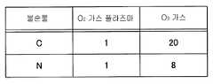
우선, 산화제에 대하여 실험을 행하였다. Si 소스 가스로서 BTBAS를 이용하고, 산화 처리에 O2 가스 플라즈마를 이용하고, 이들을 교대로 공급함으로써 SiO2 막을 성막하였다. 여기서는, 처리 용기 내에 300 mm 웨이퍼를 100 매 삽입하고, 성막 온도를 100℃로 하고, BTBAS의 공급량을 30 mL/min(sccm), 압력을 53 Pa로 하여 공정(S1)을 30 sec 행하고, O2 가스의 공급량을 2000 mL/min(sccm), 압력을 665 Pa, 13.56 MHz의 고주파 파워를 50 W로 하여 공정(S2)을 40 sec 행하고, 이들을 42 사이클 반복하여 SiO2 막을 성막한다. 또한, 처리 용기 내를 퍼지(purge)하기 위해, 공정(S1) 전에는 처리 용기 내를 진공 배기하면서 3500 mL/min(sccm)의 유량으로 퍼지 가스로서 N2 가스를 7 sec 동안 공급하고, 공정(S2) 전에는 처리 용기 내를 진공 배기하면서 3500 mL/min(sccm)의 유량으로 퍼지 가스로서 N2 가스를 6 sec 동안 공급하였다.First, an experiment was conducted with respect to an oxidizing agent. A SiO2 film was formed by using BTBAS as the Si source gas, using an O2 gas plasma for the oxidation treatment, and alternately supplying them. Here, 100 sheets of 300 mm wafers were inserted into the processing container, the film formation temperature was set to 100 ° C, the step (S1) was performed for 30 sec at a supply rate of BTBAS of 30 mL / min (sccm) and a pressure of 53 Pa.The step (S2) is performed for 40 sec at a supply rate of2 gas of 2000 mL / min (sccm), a pressure of 665 Pa, and a high frequency power of 13.56 MHz at 50 W, and these cycles are repeated 42 cycles to form a SiO2 film. In addition, in order to purge the inside of the processing vessel, N2 gas is supplied as a purge gas for 7 sec at a flow rate of 3500 mL / min (sccm) while evacuating the inside of the processing vessel before the step (S1). Prior to S2), N2 gas was supplied for 6 sec as a purge gas at a flow rate of 3500 mL / min (sccm) while evacuating the processing vessel.
비교를 위해, 공정(S2)의 산화 처리 시의 산화제로서, O3 가스를 플라즈마화하지 않고, 250 g/Nm3의 유량으로 공급한 이외에는 상기 조건과 동일하게 하여 SiO2 막을 성막하였다.For comparison, a SiO2 film was formed under the same conditions as above except that the O3 gas was supplied at a flow rate of 250 g / Nm3 as a oxidant at the time of oxidation treatment in the step (S2) without plasmaation.
그 결과, 본 발명의 실시예에 기초하여, 산화제로서 O2 가스 플라즈마 중의, 산소 래디컬을 포함하는 산소종을 이용한 경우에는, 산소를 래디컬화하지 않는 O3 가스를 이용한 경우보다 5 배 정도의 성막률(속도)을 얻을 수 있음이 확인되었다. 또한, O2 가스 플라즈마를 이용한 경우에는, 막 두께의 면 내 불균일도 매우 작다는 것도 확인되었다.As a result, based on the embodiment of the present invention, when oxygen species containing oxygen radicals in an O2 gas plasma were used as the oxidizing agent, film formation was about five times higher than when O3 gas without radicalizing oxygen was used. It was confirmed that the rate (speed) can be obtained. In addition, O was confirmed that the case where thesecond gas plasma is very small even in non-uniform surface of the film thickness.
이어서, 성막 온도에 대하여 실험을 행하였다.Next, experiment was performed about the film-forming temperature.
여기에서는, Si 소스 가스로서 BTBAS를 이용하고, 산화 처리에 O2 가스 플라즈마를 이용하고, 성막 온도 이외에는 상기 실험과 동일하게 하여 성막을 행하였다. 온도는 실온(25℃), 75℃, 100℃, 200℃, 300℃으로 변화시켜 실험을 행하였다.Here, BTBAS was used as the Si source gas, O2 gas plasma was used for the oxidation treatment, and film formation was performed in the same manner as in the above experiment except for the film formation temperature. The temperature was changed to room temperature (25 degreeC), 75 degreeC, 100 degreeC, 200 degreeC, and 300 degreeC, and the experiment was performed.
그 결과, 100℃ 이하라고 하는 저온에서도 높은 성막률로 성막할 수 있고, 실온에서도 충분히 실용적인 성막이 가능하다는 것이 확인되었다. 또한, 100℃ 이하, 특히 25℃(실온) ~ 75℃이라고 하는 저온역에서는, 높은 성막률로 균일성이 높은 막 두께를 얻을 수 있음이 확인되었다. 또한, 성막 온도가 300℃를 넘으면 막 두께 불균일이 커지고, 성막 온도는 300℃ 이하가 바람직함이 확인되었다. 특히, 레지스트 패턴 상에 성막하는 경우에는 100℃ 이하가 바람직하다는 것은 전술한 바와 같다.As a result, it was confirmed that the film can be formed at a high film forming rate even at a low temperature of 100 ° C. or lower, and that the film can be sufficiently practical at room temperature. Moreover, it was confirmed that a film thickness with high uniformity can be obtained at a high film-forming rate in 100 degrees C or less, especially 25 degreeC (room temperature)-75 degreeC. Moreover, when film-forming temperature exceeded 300 degreeC, the film thickness nonuniformity became large and it was confirmed that 300 degreeC or less is preferable for film-forming temperature. In particular, when forming a film on a resist pattern, it is as mentioned above that 100 degrees C or less is preferable.
이어서, 하드닝 처리 시의 불순물 농도를 측정하였다.Next, the impurity concentration at the time of hardening treatment was measured.
여기에서는, Si 소스 가스로서 BTBAS를 이용하고, 산화 처리에 O2 가스 플라즈마를 이용하여 성막한 경우와, O3 가스를 이용하여 성막한 경우에, 불순물로서 탄소(C) 및 질소(N)의 농도를 비교해 보았다. 측정은, 2 차 이온 질량 분석(SIMS)을 이용하여 행하였다.Here, when BTBAS is used as the Si source gas, and film formation is carried out using an O2 gas plasma for oxidation treatment and when film formation is performed using O3 gas, carbon (C) and nitrogen (N) are impurities. The concentrations were compared. The measurement was performed using secondary ion mass spectrometry (SIMS).
그 결과를 도 12에 도시한다. 이 도에 도시한 바와 같이, O2 가스 플라즈마를 이용하여 성막한 경우의 탄소(C)의 농도 및 질소(N)의 농도를 각각 “1”로서 규격화했을 때, O3 가스를 이용하여 성막한 경우에는, 탄소(C)의 농도는 20 배, 질소(N)의 농도는 8 배라고 하는 측정 결과를 얻을 수 있었다. 이 결과로부터, 하드닝 처리에, O2 가스 플라즈마를 이용하여 성막하는 것이, 불순물의 저감에 효과적임이 확인되었다. 포토레지스트는 일반적으로 암모니아에 약하고, 암모니아의 발생이 포트레지스트 포이즈닝(poisoning)의 한 요인이 된다. 암모니아의 발생을 억제하기 위해서는, 질소(N)의 발생을 억제하는 것이 효과적이다. O2 가스 플라즈마를 이용하여 산화 처리하면, 질소(N)의 발생량을 적게 억제할 수 있으므로, 포트레지스트 포이즈닝을 억제할 수 있게 된다. 이는, 하드닝 처리에 유리하다.The result is shown in FIG. As shown in this figure, when the concentration of carbon (C) and the concentration of nitrogen (N) in the case of film formation using an O2 gas plasma are normalized as "1", respectively, film formation using O3 gas is performed. In the case, the measurement result that the concentration of carbon (C) is 20 times and the concentration of nitrogen (N) is 8 times was obtained. From this result, it was confirmed that forming a film using O2 gas plasma for hardening treatment is effective for reducing impurities. Photoresists are generally vulnerable to ammonia, and the generation of ammonia is a factor in potash poisoning. In order to suppress the generation of ammonia, it is effective to suppress the generation of nitrogen (N). When the oxidation treatment is performed using an O2 gas plasma, the amount of nitrogen (N) generated can be reduced to a low degree, so that potash poisoning can be suppressed. This is advantageous for the hardening treatment.
이와 같이, 제 1 실시예에 의하면, 해상 한계 이하의 피치를 갖는 미세 패턴을 형성할 수 있다. 이와 함께, 실리콘 산화막(104)을, 유기 실리콘을 포함하는 소스 가스와, 플라즈마에 의하여 생성된, 산소 래디컬 등의 산소종을 포함하는 가스를 교대로 공급하여 형성함으로써, 레지스트 패턴(103’)의 내열 온도 이하의 매우 낮은 온도로, 또한 막 두께의 제어성도 좋게 형성할 수 있다. 또한, 질소(N)의 발생을 억제하므로, 포토레지스트 포이즈닝을 억제하는 것도 가능해진다. 그 결과, 실리콘 산화막(104)의 막 두께를 분자 레벨에서 제어할 수 있고, CD 제어가 용이하게 되며, CD 균일성의 확보가 양호하게 이루어진다.Thus, according to the first embodiment, it is possible to form a fine pattern having a pitch below the resolution limit. In addition, the
이와 같이 하여 형성된 박막(102)의 미세 패턴은, 예를 들면 트랜지스터의 게이트 전극 또는 반도체 메모리의 비트선과 같이, 고밀도로 배치되는 집적 회로 패턴에 이용할 수 있다.The fine pattern of the
(제 2 실시예)(Second embodiment)
도 13은, 본 발명의 제 2 실시예에 따른 패터닝 방법의 주요 제조 공정을 도시한 단면도이다.13 is a cross-sectional view showing the main manufacturing process of the patterning method according to the second embodiment of the present invention.
도 13에 도시한 바와 같이, 제 2 실시예는 제 1 실시예에서 설명한 제 1 회 트리밍 처리와 하드닝 처리를 동일한 성막 장치 내에서 연속 처리하도록 한 것이다(in-situ 처리).As shown in Fig. 13, in the second embodiment, the first trimming processing and the hardening processing described in the first embodiment are continuously processed in the same film forming apparatus (in-situ processing).
트리밍 처리는 에칭 장치 또는 애싱 장치 등을 이용하여 행하여지고, 이에 대하여 하드닝 처리는 성막 장치를 이용하여 행하여진다. 이 때문에, 일반적으로 트리밍 처리를 끝낸 반도체 기판(웨이퍼)은, 애싱 장치로부터 일단 인출된 후, 성막 장치에 반송된다.The trimming treatment is performed using an etching apparatus, an ashing apparatus, or the like, while the hardening treatment is performed using a film forming apparatus. For this reason, generally the semiconductor substrate (wafer) which finished the trimming process is once taken out from an ashing apparatus, and is conveyed to the film-forming apparatus.
이와 같이, 트리밍 처리 후, 웨이퍼가 장치로부터 인출되므로, 레지스트 패턴(103’)의 표면에 먼지 등이 부착될 가능성이 있다. 레지스트 패턴(103’)의 표면에 먼지 등이 부착되면, 레지스트 패턴(103’) 상에 형성되는 실리콘 산화막(104)에서는 결함 밀도가 증가하고, 또한 그 막 두께의 균일성이 쉽게 악화된다.Thus, since the wafer is taken out from the apparatus after the trimming treatment, dust or the like may adhere to the surface of the resist
이에 대하여, 제 2 실시예에 의하면, 트리밍 처리를 성막 장치에서 행하고, 또한, 트리밍 처리와 하드닝 처리를 동일한 성막 장치 중에서 연속적으로 행한다. 이에 의해, 레지스트 패턴(103’)의 표면을 청정하게 유지한 채로, 실리콘 산화막(104)을 성막할 수 있어, 그 결함 밀도를 저감시키고, 또한 막 두께의 균일성을 높일 수 있다고 하는 이점이 발생된다.In contrast, according to the second embodiment, the trimming process is performed in the film forming apparatus, and the trimming process and the hardening process are continuously performed in the same film forming apparatus. Thereby, the advantage that the
또한, 두 처리를 동일 장치 내에서 연속적으로 행함으로써, 반송 또는 대기 시간(Queuing-time)을 저감하여, 생산 효율을 향상시켜 비용을 저감할 수 있다고 하는 효과도 있다.In addition, by carrying out the two processes continuously in the same apparatus, there is an effect that it is possible to reduce the conveying or waiting time (Queuing-time), improve the production efficiency and reduce the cost.
이 제 2 실시예에 따른 패터닝 방법에 사용되는 성막 장치의 일예를 도 14에 도시한다.An example of the film-forming apparatus used for the patterning method which concerns on this 2nd Example is shown in FIG.
도 14에 도시한 바와 같이, 제 2 실시예에 따른 패터닝 방법에 사용되는 성막 장치(80’)의 기본 구성은, 도 8에 도시한 성막 장치(80)와 마찬가지이며, 특히 산소 함유 가스 공급 기구(14)와, Si 소스 가스 공급 기구(15)와, 플라즈마 생성 기구(30)를 구비하고 있으므로, 제 1 실시예에서 설명한 실리콘 산화막(104)의 성막과 동일한 성막을 행할 수 있다.As shown in FIG. 14, the basic structure of the film-forming apparatus 80 'used for the patterning method which concerns on 2nd Example is the same as that of the film-forming
또한, 성막 장치(80’)는, 오존 함유 가스 공급 기구(14’)를 구비하고 있다. 오존 함유 가스 공급 기구(14’)는 오존 함유 가스 공급원(17’)을 구비하고, 이 오존 함유 가스 공급원(17’)은 유량 제어기(18d) 및 개폐 밸브(18c)를 거쳐, 예를 들면 산소 함유 가스 배관(18)에 접속되어 있다. 이에 의해, 오존 함유 가스를 처리 용기(1) 내로 공급할 수 있다The film forming apparatus 80 'includes an ozone-containing gas supply mechanism 14'. The ozone-containing gas supply mechanism 14 'includes an ozone-containing gas supply source 17', and this ozone-containing gas supply source 17 'passes through the
트리밍 처리 시에는, 오존 함유 가스, 예를 들면 오존 가스를 이용한다. 오존 가스를 이용하여 트리밍 처리할 때에는 플라즈마를 생성하지 않아도 좋다. 이 때문에, 오존 함유 가스는, 예를 들면, 플라즈마 생성 기구(30)에서는 플라즈마 전극(33)에 고주파 전압을 인가하지 않는 상태에서, 분산 노즐(19)을 거쳐 처리 용기(1) 내로 공급하도록 하면 된다.At the time of trimming treatment, ozone-containing gas, for example ozone gas, is used. When trimming using ozone gas, it is not necessary to generate plasma. For this reason, when the ozone containing gas is supplied into the
도 14에 도시한 성막 장치(80’)에 의하면, 산소 함유 가스 공급 기구(14), Si 소스 가스 공급 기구(15) 및 플라즈마 생성 기구(30)에, 추가로 오존 함유 가스 공급 기구(14’)를 구비하고 있으므로, 처리 용기(1) 내에서 오존 함유 가스를 이용하여 레지스트 패턴(103)을 트리밍 처리한 후, 동일한 처리 용기(1) 내에서 유기 실리콘을 포함하는 소스 가스와, 플라즈마에 생성된 산소 래디컬 등의 산소종을 포함하는 가스를 교대로 공급하면서 실리콘 산화막(104)을 성막할 수 있다. 따라서, 레지스트 패턴(103’)의 표면을 청정하게 유지한 채로, 제 1 실시예에서 설명한 방법으로 실리콘 산화막(104)을 성막할 수 있고, 제 1 실시예에 비해, 실리콘 산화막(104)의 결함 밀도를 저감시키고, 또한 막 두께의 균일성을 높일 수 있다고 하는 이점이 발생된다.According to the
(제 3 실시예)(Third embodiment)
도 15 내지 도 23은, 본 발명의 제 3 실시예에 따른 패터닝 방법을 주요 제조 공정마다 도시한 단면도이다.15 to 23 are cross-sectional views showing the patterning method according to the third embodiment of the present invention for each major manufacturing step.
제 3 실시예는, 본 발명에 따른 패터닝 방법을, 실제의 반도체 프로세스에 보다 적합하게 적용할 수 있는 일예를 도시한 것이다.The third embodiment shows an example in which the patterning method according to the present invention can be more suitably applied to an actual semiconductor process.
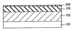
우선, 도 15에 도시한 바와 같이, 제 1 실시예와 마찬가지로, 반도체 기판(101) 상에, 박막(102), 예를 들면 도전성 실리콘막을 형성한 후, 박막(102) 상에 하드마스크막(106)을 형성한다. 하드마스크막(106)은 박막(102)과 다른 막으로 이루어지고, 또한, 박막(102)에 대하여 에칭 선택비를 실현할 수 있는 막으로 이루어진다. 예를 들면, 박막(102)이 도전성 실리콘막인 경우에는, 하드마스크막(106)에는, 예를 들면 실리콘 질화막 등이 선택된다. 이어서, 하드마스크막(106) 상에 반사 방지막(200)을 형성한다.First, as shown in FIG. 15, similarly to the first embodiment, a
이어서, 도 16에 도시한 바와 같이, 반사 방지막(200) 상에 포토레지스트를 도포하고, 포토레지스트막을 형성한다. 이어서, 포토리소그래피 기술을 이용하여, 포토레지스트막을 소정의 피치(p1)를 갖는 레지스트 패턴(103)으로 가공한다. 본 실시예에서는, 제 1 실시예와 마찬가지로, 레지스트 패턴(103)은, 예를 들면 라인·앤드·스페이스 패턴을 가지고, 소정의 피치(p1)로서는 노광 장치의 해상 한계 정도로 한다.Next, as shown in FIG. 16, a photoresist is apply | coated on the
이어서, 도 17에 도시한 바와 같이, 레지스트 패턴(103)을 트리밍하고, 트리밍된 레지스트 패턴(103’)을 얻는다(제 1 회 트리밍 처리). 트리밍 처리의 조건은 제 1 실시예와 동일한 조건이면 된다.Next, as shown in FIG. 17, the resist
이어서, 도 18에 도시한 바와 같이, 트리밍된 레지스트 패턴(103’) 및 반사 방지막(200) 상에 실리콘 산화막(104)을 형성한다(하드닝 처리). 제 3 실시예에서도 실리콘 산화막(104)의 형성은 제 1 실시예와 마찬가지이며, 유기 실리콘을 포함하는 소스 가스와, 플라즈마에 의하여 생성된, 산소 래디컬 등의 산소종을 포함하는 가스를 교대로 공급하면서 형성된다.Next, as shown in FIG. 18, the
이어서, 도 19에 도시한 바와 같이, 실리콘 산화막(104) 상에 반사 방지막(201)을 형성한다. 이어서, 반사 방지막(201) 상에 포토레지스트를 도포하고, 포토레지스트막을 형성한다. 이어서, 포토리소그래피 기술을 이용하여, 포토레지스트막을 소정의 피치(p2)를 갖는 레지스트 패턴(105)으로 가공한다. 본 실시예에서는, 레지스트 패턴(105)은, 트리밍된 레지스트 패턴(103’)과 마찬가지로 라인·앤드·스페이스 패턴을 갖는다. 또한, 레지스트 패턴(105)의 소정의 피치(p2)는 노광 장치의 해상 한계 정도로 한다. 또한, 본 실시예의 레지스트 패턴(105)은 트리밍된 레지스트 패턴(103’) 사이에 배치되고, 레지스트 패턴(103’)과 레지스트 패턴(105)이 교대로 배치된다.Subsequently, as shown in FIG. 19, an
이어서, 도 20에 도시한 바와 같이, 레지스트 패턴(105)을 트리밍하고, 트리밍된 레지스트 패턴(105’)을 얻는다(제 2 회 트리밍 처리). 트리밍 처리의 조건은 제 1 실시예와 동일한 조건이면 된다. 제 2 회 트리밍 처리에 의하여, 레지스트 패턴(103’ 및 105’)으로 이루어진 레지스트 패턴이 형성되고, 제 1 실시예와 마찬가지로, 해상 한계 이하의 피치를 갖는 레지스트 패턴이 형성된다.Next, as shown in FIG. 20, the resist
이어서, 도 21에 도시한 바와 같이, 레지스트 패턴(103’ 및 105’)을 에칭 마스크로 이용하여 반사 방지막(201, 200) 및 실리콘 산화막(104)을 에칭하고, 또한, 도 22에 도시한 바와 같이, 하드마스크막(106)을 에칭한다.Next, as shown in FIG. 21, the
이어서, 도 23에 도시한 바와 같이, 반사 방지막(201, 200), 실리콘 산화막(104), 레지스트 패턴(103’ 및 105’)을 제거한 후, 하드마스크막(106)을 에칭 마스크로 이용하여 박막(102)을 에칭하고, 박막(102)을 원하는 미세 패턴으로 가공한다. 하드마스크막(106)의 피치(p3’)는 레지스트 패턴(103’ 및 105’)의 피치(p3)와 거의 동일하며, 해상 한계 이하이다. 따라서, 하드마스크막(106)을 에칭 마스크로 이용하여 에칭된 박막(102)의 피치(p4)는 해상 한계 이하가 된다. 이와 같이 하여, 제 3 실시예에서는, 해상 한계 이하의 피치를 갖는 미세 패턴을 형성할 수 있다.Next, as shown in FIG. 23, after removing the
제 3 실시예에서도, 하드닝 처리 시, 유기 실리콘을 포함하는 소스 가스와, 플라즈마에 의해 여기된, 산소 래디컬 등의 산소종을 포함하는 가스를 교대로 공급하여 실리콘 산화막(104)을 형성하므로, 제 1 실시예와 마찬가지로, 해상 한계 이하의 피치를 갖는 미세 패턴의 CD 균일성을 보다 양호하게 할 수 있다.Also in the third embodiment, during the hardening process, the
또한, 제 3 실시예에 의하면, 박막(102)을 하드마스크막(106)을 에칭 마스크로 이용하여 에칭하므로, 레지스트 패턴(103’ 및 105’)을 에칭 마스크로 이용하여 에칭하는 경우에 비해, 막 두께가 두꺼운 박막(102)을 가공할 수 있다고 하는 이점이 발생된다.Further, according to the third embodiment, since the
또한, 제 3 실시예는 제 2 실시예와 조합할 수 있으며, 제 1 회 트리밍 처리(도 17 참조)와 하드닝 처리(도 18 참조)를 동일한 성막 장치 중에서 연속 처리할 수 있다. 이 경우에는, 제 2 실시예와 마찬가지로, 레지스트 패턴(103’)의 표면을 청정하게 유지한 채로 실리콘 산화막(104)을 성막할 수 있으므로, 실리콘 산화막(104)의 막 두께의 균일성을 보다 높일 수 있게 된다.Further, the third embodiment can be combined with the second embodiment, and the first trimming process (see FIG. 17) and the hardening process (see FIG. 18) can be continuously processed in the same film forming apparatus. In this case, as in the second embodiment, since the
(제 4 실시예)(Example 4)
도 24a 내지 도 24i는, 본 발명의 제 4 실시예에 따른 패터닝 방법을 주요 제조 공정마다 도시한 단면도이다.24A to 24I are sectional views showing the patterning method according to the fourth embodiment of the present invention for each major manufacturing step.
우선, 도 24a에 도시한 바와 같이, 제 1 실시예와 마찬가지로, 반도체 기판(101) 상에 박막(102)을 형성한다. 본 명세서에서는, 반도체 기판(101)은, 반도체, 예를 들면, 실리콘 기판만을 도시한 것이 아니라, 반도체 기판 내, 또는 반도체 기판 상에 형성된 반도체 소자 또는 집적 회로 패턴에 대응한 도전막, 이들을 절연하는 층간 절연막이 형성된 구조체를 포함한다. 박막(102)은, 후에 미세 패턴으로 가공되는 막이며, SiN 또는 SiO2의 절연막이어도 좋고, 도전성 폴리실리콘과 같은 도전막이어도 좋다. 본 실시예에서는, 일예로서 박막(102)을 SiN으로 한다. 이어서, 박막(102) 상에 반사 방지 재료를 도포하고, 반사 방지막(BARC)(200)을 형성한다.First, as shown in FIG. 24A, the
이어서, 도 24b에 도시한 바와 같이, 반사 방지막(200) 상에 포토레지스트를 도포하고, 포토레지스트막을 형성하고, 포토리소그래피 기술을 이용하여 포토레지스트막을 가공하여, 소정의 피치(p1)를 갖는 레지스트 패턴(103)을 얻는다. 본 실시예에서는, 레지스트 패턴(103)은 라인·앤드·스페이스 패턴을 가지고, 소정의 피치(p1)는 노광 장치의 해상 한계 정도로 한다.Subsequently, as shown in FIG. 24B, a photoresist is applied on the
이어서, 도 24c에 도시한 바와 같이, 레지스트 패턴(103)을 트리밍하고, 트리밍된 레지스트 패턴(103’)을 얻는다(본 명세서에서는 제 1 회 트리밍 처리라고 함). 트리밍 처리는, 예를 들면 산소 래디컬 또는 오존 가스를 포함하는 분위기 중에서, 실온 ~ 100℃의 온도에서 행해진다.Subsequently, as shown in FIG. 24C, the resist
이어서, 도 24d에 도시한 바와 같이, 트리밍된 레지스트 패턴(103’) 및 반사 방지막(200) 상에, 박막(102), 반사 방지막(200) 및 레지스트 패턴(103’)과는 다른 실리콘 산화막(104)을 형성한다(하드닝 처리). 실리콘 산화막(104)은, 선행하는 실시예와 마찬가지로, 도 8 내지 도 10을 참조하면서 설명한 성막 장치(80) 또는 도 14를 참조하면서 설명한 성막 장치(80’)를 이용하여 형성할 수 있다.Next, as shown in FIG. 24D, on the trimmed resist
이어서, 도 24e에 도시한 바와 같이, 실리콘 산화막(104) 상에 반사 방지 재료를 도포하고, 반사 방지막(BARC)(201)을 형성한다. 반사 방지막(201)의 두께는 그 표면이 거의 평탄하게 되는 정도이며, 이에 의해, 레지스트 패턴(103’)에 의하여 발생하는 고저(高低)차가 충분히 저감된다.Next, as shown in FIG. 24E, an antireflection material is applied on the
이어서, 반사 방지막(201) 상에 포토레지스트를 도포하고, 포토레지스트막을 형성한다. 이 후, 도 24f에 도시한 바와 같이, 포토리소그래피 기술에 의하여 포토레지스트막을 가공하여, 소정의 피치(p2)를 갖는 레지스트 패턴(105)을 형성한다. 본 실시예에서는, 레지스트 패턴(105)은, 트리밍된 레지스트 패턴(103’)과 마찬가지로 라인·앤드·스페이스 패턴을 가지고 있다. 또한, 레지스트 패턴(105)의 소정의 피치(p2)는 노광 장치의 해상 한계 정도로 한다. 또한, 본 실시예의 레지스트 패턴(105)은 트리밍된 레지스트 패턴(103’) 사이에 배치되고, 레지스트 패턴(103’)과 레지스트 패턴(105)이 교대로 배치된다.Next, a photoresist is applied on the
이어서, 제 2 회째의 트리밍 처리를 행한다. 즉, 도 24g에 도시한 바와 같이, 레지스트 패턴(105)을 트리밍하고, 트리밍된 레지스트 패턴(105’)을 얻는다(도 24h). 이 트리밍 처리는, 예를 들면 산소 래디컬 또는 오존 가스를 포함하는 분위기 중에서, 실온 ~ 100℃의 온도에서 행할 수 있다. 지금까지 설명한 순서에 의하여, 레지스트 패턴(103’)과 레지스트 패턴(105’)이라고 하는 2 개의 레지스트 패턴이 형성된다. 이들 2 개의 레지스트 패턴(103’, 105’)은, 후술하는 바와 같이, 실질적으로 하나의 레지스트 패턴으로서 기능한다. 이 레지스트 패턴은, 패턴(103’ 및 105’)이 교대로 배치된 패턴이므로, 그 피치(p3)는 피치(p1 및 p2)보다 좁은 피치, 본 실시예에서는, 피치(p1 및 p2)의 거의 1/2의 피치가 된다. 이와 같이, 각각 형성된 레지스트 패턴(103’ 및 105’)을 교대로 배치함으로써, 해상 한계 이하의 피치를 갖는 레지스트 패턴을 형성할 수 있다.Next, a 2nd trimming process is performed. That is, as shown in Fig. 24G, the resist
이어서, 도 24i에 도시한 바와 같이, 레지스트 패턴(103’ 및 105’)을 에칭 마스크로 이용하여, 반사 방지막(201, 200), 실리콘 산화막(104) 및 박막(102)을 에칭하고, 박막(102)을 원하는 미세 패턴으로 가공한다. 가공된 박막(102)의 피치(p4)는, 레지스트 패턴(103’ 및 105’)의 피치(p3)와 거의 동일해지므로, 박막(102)으로 이루어진 미세 패턴의 피치(p4)는 해상 한계 이하로 할 수 있다. 이와 같이 하여, 제 4 실시예에서는, 해상 한계 이하의 피치를 갖는 미세 패턴을 형성할 수 있다.Next, as shown in FIG. 24I, the
또한, 제 4 실시예에 의한 미세 패턴 형성 방법에 의하면, 레지스트 패턴(103’)의 보호막으로서의 실리콘 산화막(104) 상에, 표면이 평탄해지는 정도의 두께를 갖는 반사 방지막(201)이 형성되므로, 반사 방지막(201) 상에, 윤곽이 보다 명확한 레지스트 패턴(105(105’))을 형성할 수 있게 된다. 따라서, 레지스트 패턴(103’ 및 105’)을 마스크 층으로서 이용한 박막(102)의 에칭에서의 에칭 정밀도를 전체적으로 높일 수 있다.Further, according to the method for forming a fine pattern according to the fourth embodiment, since the
또한, 본 발명은, 상기 실시예에 한정되지 않고, 다양한 변형이 가능하다. 예를 들면, 상기 실시예에서는, 본 발명을 복수의 반도체 웨이퍼를 탑재하여 일괄적으로 성막을 행하는 뱃치(batch)식의 성막 장치에 적용한 예를 도시하였으나, 이에 한정되지 않고, 1 매의 웨이퍼마다 성막을 행하는 매엽식의 성막 장치에 적용할 수도 있다. 또한, 에톡시실란 가스 및 아미노실란 가스로서는, 상기 실시예에 도시한 것에 한정되지 않는다. 또한, 산화제로서 다양한 산소 함유 가스를 플라즈마화함으로써 생성한 산소 래디컬 등을 도시하였으나, 이에 한정되지 않고, 산소 래디컬 등의 산소종을 생성할 수 있는 한, 어떠한 가스라도 이용할 수 있다. 또한, 상술한 산소종은 플라즈마에 의하지 않고, 다양한 산소 함유 가스에 레이저 광 또는 자외역 광(파장 : 약 350 nm 이하)을 조사하여 산소 분자 등을 활성화함으로써 생성해도 좋고, 또한, 산소 함유 가스를 열적으로 활성화함으로써 생성해도 좋다.In addition, this invention is not limited to the said Example, A various deformation | transformation is possible. For example, in the above embodiment, an example in which the present invention is applied to a batch type film forming apparatus in which a plurality of semiconductor wafers are mounted and formed in a batch is illustrated, but the present invention is not limited thereto. It can also be applied to a single film type film forming apparatus for forming a film. In addition, as an ethoxysilane gas and an aminosilane gas, it is not limited to what was shown in the said Example. In addition, although the oxygen radicals etc. which were produced | generated by making various oxygen containing gas into plasma were shown as an oxidizing agent, it is not limited to this, Any gas can be used as long as oxygen species, such as oxygen radicals, can be produced | generated. In addition, the above-mentioned oxygen species may be produced by irradiating various oxygen-containing gases with laser light or ultraviolet light (wavelength: about 350 nm or less) and activating oxygen molecules or the like without using plasma, and generating oxygen-containing gas. You may produce by thermally activating.
또한, 상기 실시예에서는, Si 소스 가스와 플라즈마에 의하여 여기된 산소종을 포함하는 가스를 완전히 교대로 공급하였으나, Si 소스 가스를 공급할 때에도, 플라즈마 등에 의해 활성화(여기)된 산소종을 포함하는 가스를 공급하도록 해도 좋다.Further, in the above embodiment, the Si source gas and the gas containing oxygen species excited by the plasma are completely supplied alternately, but when the Si source gas is supplied, the gas containing oxygen species activated (excited) by the plasma or the like is also supplied. May be supplied.
또한, 상기의 실시예에서 설명한 패터닝 방법은, 이하의 프로세스를 계속 행함으로써, 반도체 장치를 제조하는 방법으로 발전시킬 수 있다. 즉, 에칭 대상인 박막(102)이, 산화 실리콘, 산질화 실리콘, 질화 실리콘 등의 절연성의 재료로 형성되는 경우, 박막(102)을 에칭하여 미세 패턴을 얻는 단계를 행한 후(도 7, 도 23, 도 24i 참조), 이 에칭에서 에칭 마스크로서 사용한 레지스트 패턴(103’, 105’) 등을 제거하는 단계를 행하면, 도 25a에 도시한 바와 같이, 반도체 기판(101) 상에 미세 패턴(이하, 편의상 절연막(102a)이라고 함)만이 남는다. 이어서, 절연막(102a)의 간극을, 반도체, 예를 들면 실리콘으로 매립하는 단계와, 매립한 반도체를 평탄화하여 절연막(102a)의 상면을 노출시키는 단계를 행하면, 도 25b에 도시한 바와 같이, 절연막(102a)과 실리콘부(110a)가 교대로 배열되어 형성된다. 이와 같이 하면, 실리콘부(110a)를 소자 영역으로 하고, 절연막(102a)을 소자 분리 영역으로 하는 반도체 장치를 제조할 수 있게 된다. 또한, 절연막(102a)의 간극을 반도체로 매립할 때, 반도체에 소정의 불순물을 첨가하여 전도 제어(전도형 및/또는 전도도의 제어)를 행해도 좋다. 또한, 레지스트 패턴(103’, 105’) 등을 제거하는 단계를 행하지 않고, 반도체로 매립하는 단계를 행해도 좋다. 이와 같이 해도, 평탄화하는 단계에서 레지스트 패턴(103’, 105’) 등을 제거할 수 있기 때문이다. 단, 레지스트 패턴(103’, 105’) 등을 제거하는 편이, 절연막(102a)의 간극을 반도체로 매립할 때에 에스펙트비를 작게할 수 있다는 점에서 바람직하다.The patterning method described in the above embodiment can be developed into a method of manufacturing a semiconductor device by continuing the following process. That is, when the
또한, 에칭 대상인 박막(102)이, 반도체, 예를 들면 실리콘으로 형성되는 경우, 박막(102)을 에칭하여 미세 패턴을 얻는 단계를 행한 후(도 7, 도 23, 도 24i 참조), 이 에칭에서 에칭 마스크로서 사용한 레지스트 패턴(103’, 105’) 등을 제거하는 단계를 행하면, 미세 패턴(이하, 편의상 실리콘막(102b)이라고 함)만이 반도체 기판(101) 상에 남는다. 이어서, 실리콘막(102b)의 간극을, 산화 실리콘, 산질화 실리콘, 질화 실리콘 등의 절연성의 재료로 매립하는 단계와, 매립한 절연성의 재료를 평탄화하여 실리콘막(102b)의 상면을 노출시키는 단계를 행하면, 도 26b에 도시한 바와 같이, 실리콘막(102b)과 절연부(110b)가 교대로 배열되어 형성된다. 이와 같이 하면, 실리콘막(102b)을 소자 영역으로 하고, 절연부(110b)를 소자 분리 영역으로 하는 반도체 장치를 제조할 수 있게 된다. 또한, 박막(102)을 반도체로 형성하는 경우, 사전에, 이온 주입법(Ion Implantation)에 의하여 박막(102)에 소정의 불순물을 첨가하여 전도 제어(전도형 및/또는 전도도의 제어)를 행해도 좋다. 또한, 박막(102)을 CVD 등에 의하여 형성하는 경우에, 소정의 도펀트 가스를 이용하여 불순물을 첨가하여 전도 제어를 행해도 상관없다. 또한, 레지스트 패턴(103’, 105’) 등을 제거하는 단계를 행하지 않고, 절연성의 재료로 매립하는 단계를 행해도 좋다. 이와 같이 해도, 평탄화하는 단계에서 레지스트 패턴(103’, 105’) 등을 제거할 수 있기 때문이다. 단, 레지스트 패턴(103’, 105’) 등을 제거하는 편이, 실리콘막(102b)의 간극을 절연성의 재료로 매립할 때에 에스펙트비를 작게할 수 있다 점에서 바람직하다.In addition, when the
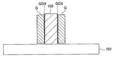
또한, 제 1 내지 제 3 실시예에 따른 패터닝 방법은, 일예로서 도 27에 도시한 반도체 장치의 제조에 이용할 수 있다. 도 27은, 반도체로 형성되고, 제 1 내지 제 3 실시예 중 어느 하나의 패터닝 방법에 의하여 형성된 박막(102)과, 이 박막(102)을 개재하도록 형성된 절연층(GOX)과, 절연층(GOX)에 접하는 전극층(G)을 구비하는, 소위 Fin형 전계 효과 트랜지스터(FET)의 단면도이다. 본 발명의 실시예에 의한 패터닝 방법에 의하면, 포토리소그래피에 이용할 수 있는 노광 장치의 해상 한계 치수보다 좁은 폭을 갖는 박막(102)을 형성할 수 있으므로, Fin형 FET를 미세화할 수 있고, 집적 밀도의 향상이 가능해진다.The patterning method according to the first to third embodiments can be used for manufacturing the semiconductor device shown in FIG. 27 as an example. 27 is a
또한, 상기 실시예에서는, 플라즈마를 형성하는 기구를 처리 용기에 일체적으로 내장한 예에 대하여 설명하였으나, 이에 한정되지 않으며, 처리 용기와는 별개로 설치하여, 처리 용기의 밖에서 사전에 플라즈마화하여 처리 용기에 도입하는 리모트 플라즈마 장치를 이용하여도 좋다.In addition, in the above embodiment, an example in which a mechanism for forming plasma is integrally embedded in the processing container has been described. However, the present invention is not limited thereto, and is provided separately from the processing container so as to be plasma-formed before the processing container. You may use the remote plasma apparatus introduce | transduced into a processing container.
또한, 성막 장치(80, 80’)의 웨이퍼 보트(5)는, 50 ~ 100 매의 웨이퍼(W)를 탑재할 수 있다고 설명하였으나, 탑재 웨이퍼 매수는 이 범위에 한정되지 않는다. 예를 들면, 성막 장치(80, 80’)는 비교적 적은 매수의 웨이퍼, 예를 들면 2 ~ 15 매 정도를 탑재할 수 있는 웨이퍼 보트(5)를 갖고 있어도 좋다. 또한, 성막 장치(80, 80’)는 2 ~ 15 매 정도의 비교적 적은 매수의 웨이퍼를 일괄적으로 처리하는 것을 의도한, 이른바 세미·뱃치(미니·뱃치) 타입의 성막 장치로서 구성해도 좋다.In addition, although the
또한, 피처리체로서는, 반도체 웨이퍼에 한정되지 않고, LCD 글라스 기판 등의 다른 기판에도 본 발명을 적용할 수 있다.In addition, as a to-be-processed object, this invention is applicable not only to a semiconductor wafer but also to other board | substrates, such as an LCD glass substrate.
또한, 포토레지스트막을 형성하기 전에, 반사 방지막(200, 201)을 형성하였으나, 반사 방지막(200, 201)은 필요에 따라 형성하면 된다.In addition, although the
또한, 레지스트 패턴(103 및 105)의 트리밍도 필요에 따라 행하면 좋다.In addition, trimming of the resist
본 국제 출원은 2007 년 6 월 8 일에 출원된 일본특허출원 2007-153184호에 기초한 우선권을 주장하는 것이며, 2007-153184호의 전체의 내용을 여기에 원용한다.This international application claims the priority based on Japanese Patent Application No. 2007-153184 for which it applied on June 8, 2007, and uses the content of 2007-153184 here.
101 : 반도체 기판
102 : 박막
103 : 포토레지스트 패턴
103’: 트리밍된 포토레지스트 패턴
104 : 실리콘 산화막
105 : 포토레지스트 패턴
105’: 트리밍된 포토레지스트 패턴
106 : 하드마스크막
200, 201 : 반사 방지막101: semiconductor substrate
102: thin film
103: photoresist pattern
103 ': trimmed photoresist pattern
104: silicon oxide film
105: photoresist pattern
105 ': trimmed photoresist pattern
106: hard mask
200, 201: antireflection film
Claims (15)
Translated fromKorean상기 박막을 가공할 때에, 마스크가 되는 막을 형성하는 공정과,
상기 마스크가 되는 막을 소정의 피치를 갖는 라인을 포함하는 패턴으로 가공하는 패턴 가공 공정과,
상기 라인을 포함하는 패턴을 트리밍하는 트리밍 공정과,
소스 가스와 활성화된 산소종을 교대로 공급하여, 상기 라인을 포함하는 패턴 및 상기 박막 상에 산화막을 성막하는 성막 공정
을 구비하는 미세 패턴의 형성 방법으로서,
상기 트리밍 공정과 상기 성막 공정을 상기 산화막을 성막하는 성막 장치 내에서 연속적으로 행하는 것을 특징으로 하는 미세 패턴의 형성 방법.
Forming a thin film on the substrate,
When processing the said thin film, the process of forming the film used as a mask,
A pattern processing step of processing the film serving as the mask into a pattern including a line having a predetermined pitch,
A trimming process of trimming the pattern including the lines;
A film forming process of supplying a source gas and activated oxygen species alternately to form an oxide film on the pattern including the line and the thin film.
As a method of forming a fine pattern comprising:
The trimming step and the film forming step are successively performed in a film forming apparatus for forming the oxide film.
상기 박막을 가공할 때에, 제 1 마스크가 되는 막을 형성하는 공정과,
상기 제 1 마스크가 되는 막을 소정의 피치를 갖는 라인을 포함하는 제 1 패턴으로 가공하는 제 1 패턴 가공 공정과,
산화막을 성막하는 성막 장치 내에서 상기 제 1 패턴을 트리밍하는 제 1 트리밍 공정과,
상기 제 1 트리밍 공정과 연속하여, 상기 성막 장치 내로 소스 가스와 활성화된 산소종을 교대로 공급하여, 상기 제 1 트리밍 공정에 의해 트리밍된 상기 제 1 패턴 및 상기 박막 상에 산화막을 성막하는 성막 공정과,
상기 산화막 상에 제 2 마스크가 되는 막을 형성하는 공정과,
상기 제 2 마스크가 되는 막을 소정의 피치를 갖는 라인을 포함하는 제 2 패턴으로 가공하는 제 2 패턴 가공 공정과,
상기 제 2 패턴을 트리밍하는 제 2 트리밍 공정
을 구비하는 미세 패턴의 형성 방법으로서,
상기 산화막이 형성된 상기 제 1 패턴 및 트리밍된 상기 제 2 패턴을 마스크로 이용하여 상기 박막을 가공하는 것을 특징으로 하는 미세 패턴의 형성 방법.
Forming a thin film on the substrate,
When processing the said thin film, the process of forming the film used as a 1st mask,
A first pattern processing step of processing the film to be the first mask into a first pattern including a line having a predetermined pitch,
A first trimming step of trimming the first pattern in a film forming apparatus for forming an oxide film;
A film forming process in which an oxide film is formed on the first pattern and the thin film trimmed by the first trimming process by alternately supplying a source gas and activated oxygen species to the film forming apparatus in succession to the first trimming process. and,
Forming a film to be a second mask on the oxide film;
A second pattern processing step of processing the film serving as the second mask into a second pattern including a line having a predetermined pitch,
A second trimming process of trimming the second pattern
As a method of forming a fine pattern comprising:
And forming the fine pattern using the first pattern on which the oxide film is formed and the trimmed second pattern as a mask.
상기 마스크가 되는 막으로서 레지스트막을 이용하는 것을 특징으로 하는 미세 패턴의 형성 방법.
The method of claim 1,
A method of forming a fine pattern, wherein a resist film is used as the film to be the mask.
상기 패턴 가공 공정으로서 포토리소그래피 기술을 이용하여 상기 소정의 피치를 갖는 라인을 포함하는 패턴으로 가공하는 것을 특징으로 하는 미세 패턴의 형성 방법.
The method of claim 1,
A method of forming a fine pattern, comprising: processing into a pattern including a line having the predetermined pitch using photolithography as the pattern processing step.
상기 트리밍 공정은 산소 함유 가스 플라즈마 또는 오존 함유 가스를 이용하여 트리밍하는 것을 특징으로 하는 미세 패턴의 형성 방법.
The method of claim 1,
The trimming process is a method of forming a fine pattern, characterized in that for trimming using an oxygen-containing gas plasma or ozone-containing gas.
상기 소스 가스로서 아미노실란계 프리커서를 이용하는 것을 특징으로 하는 미세 패턴의 형성 방법.
The method according to claim 1 or 2,
A method of forming a fine pattern, wherein an aminosilane-based precursor is used as the source gas.
상기 아미노실란계 프리커서는, 1 가 또는 2 가의 아미노실란계 프리커서인 것을 특징으로 하는 미세 패턴의 형성 방법.
The method according to claim 6,
The aminosilane precursor is a monovalent or divalent aminosilane precursor.
상기 1 가 또는 2 가의 아미노실란계 프리커서는,
BTBAS(비스터셔리부틸아미노실란),
BDMAS(비스디메틸아미노실란),
BDEAS(비스디에틸아미노실란),
DMAS(디메틸아미노실란),
DEAS(디에틸아미노실란),
DPAS(디프로필아미노실란),
BAS(부틸아미노실란),
DIPAS(디이소프로필아미노실란),
BEMAS(비스에틸메틸아미노실란)
으로부터 선택된 적어도 1 종을 이용하는 것을 특징으로 하는 미세 패턴의 형성 방법.
The method of claim 7, wherein
The monovalent or divalent aminosilane-based precursor is,
BTBAS (Busterary Butylaminosilane),
BDMAS (bisdimethylaminosilane),
BDEAS (bisdiethylaminosilane),
DMAS (dimethylaminosilane),
DEAS (diethylaminosilane),
DPAS (dipropylaminosilane),
BAS (butylaminosilane),
DIPAS (diisopropylaminosilane),
BEMAS (bisethylmethylaminosilane)
A method for forming a fine pattern, characterized in that at least one selected from the group is used.
상기 활성화된 산소종으로서 플라즈마에 의해 여기된 산소 래디컬을 이용하는 것을 특징으로 하는 미세 패턴의 형성 방법.
The method according to claim 1 or 2,
And forming oxygen radicals excited by plasma as the activated oxygen species.
상기 플라즈마에 의해 여기된 산소 래디컬은, O2 가스, NO 가스, N2O 가스, H2O 가스, O3 가스 중 어느 하나로부터 선택되는 적어도 1 종을 플라즈마화하여 얻는 것을 특징으로 하는 미세 패턴의 형성 방법.
The method of claim 9,
The oxygen radicals excited by the plasma are obtained by plasmalizing at least one selected from any one of O2 gas, NO gas, N2 O gas, H2 O gas, and O3 gas. Method of formation.
상기 제1 마스크가 되는 막 및 상기 제2 마스크가 되는 막으로서 레지스트막을 이용하는 것을 특징으로 하는 미세 패턴의 형성 방법.
The method of claim 2,
A resist pattern is used as a film to be said first mask and a film to be said second mask.
상기 제1 패턴 가공 공정으로서 포토리소그래피 기술을 이용하여 상기 소정의 피치를 갖는 라인을 포함하는 제1 패턴으로 가공하며,
상기 제2 패턴 가공 공정으로서 포토리소그래피 기술을 이용하여 상기 소정의 피치를 갖는 라인을 포함하는 제2 패턴으로 가공하는 것을 특징으로 하는 미세 패턴의 형성 방법.
The method of claim 2,
Processing into a first pattern including a line having the predetermined pitch using photolithography technology as the first pattern processing step,
A method of forming a fine pattern, comprising: processing into a second pattern including a line having the predetermined pitch using photolithography as the second pattern processing step.
상기 제1 트리밍 공정 및 상기 제2 트리밍 공정은 산소 함유 가스 플라즈마 또는 오존 함유 가스를 이용하여 트리밍하는 것을 특징으로 하는 미세 패턴의 형성 방법.
The method of claim 2,
And the first trimming step and the second trimming step trim using an oxygen-containing gas plasma or an ozone-containing gas.
상기 처리 용기 내로 소스 가스를 공급하는 소스 가스 공급 수단과,
상기 처리 용기 내로 산소 함유 가스를 공급하는 산소 함유 가스 공급 수단과,
상기 산소 함유 가스로부터 여기된 산소 래디컬을 형성하는 플라즈마 생성 수단
을 구비하고,
상기 처리 용기 내로 상기 소스 가스와 산소 래디컬을 교대로 공급함으로써, 소정의 피치를 갖는 라인을 포함하는 패턴이 형성된 상기 기판 상에 산화막을 성막하는 성막 장치로서,
상기 산화막을 성막하기 전에 산소 래디컬을 공급함으로써, 상기 소정의 피치를 갖는 라인을 포함하는 패턴을 트리밍하는 것을 특징으로 하는 성막 장치.
A processing container for processing the substrate,
Source gas supply means for supplying a source gas into the processing container;
Oxygen-containing gas supply means for supplying an oxygen-containing gas into the processing container;
Plasma generating means for forming an oxygen radical excited from the oxygen-containing gas
And
A film forming apparatus for forming an oxide film on the substrate on which a pattern including a line having a predetermined pitch is formed by alternately supplying the source gas and the oxygen radical into the processing container,
A film forming apparatus, wherein the pattern including the line having the predetermined pitch is trimmed by supplying oxygen radicals before forming the oxide film.
상기 처리 용기 내로 소스 가스를 공급하는 소스 가스 공급 수단과,
상기 처리 용기 내로 산소 함유 가스를 공급하는 산소 함유 가스 공급 수단과,
상기 처리 용기 내로 오존 함유 가스를 공급하는 오존 함유 가스 공급 수단과,
상기 산소 함유 가스로부터 여기된 산소 래디컬을 형성하는 플라즈마 생성 수단
을 구비하고,
상기 처리 용기 내로 상기 소스 가스와 산소 래디컬을 교대로 공급함으로써, 소정의 피치를 갖는 라인을 포함하는 패턴이 형성된 상기 기판 상에 산화막을 성막하는 성막 장치로서,
상기 산화막을 성막하기 전에 오존 함유 가스를 공급함으로써, 상기 소정의 피치를 갖는 라인을 포함하는 패턴을 트리밍하는 것을 특징으로 하는 성막 장치.
A processing container for processing the substrate,
Source gas supply means for supplying a source gas into the processing container;
Oxygen-containing gas supply means for supplying an oxygen-containing gas into the processing container;
Ozone-containing gas supply means for supplying an ozone-containing gas into the processing container;
Plasma generating means for forming an oxygen radical excited from the oxygen-containing gas
And
A film forming apparatus for forming an oxide film on the substrate on which a pattern including a line having a predetermined pitch is formed by alternately supplying the source gas and oxygen radical into the processing container,
A film forming apparatus, wherein the pattern including the line having the predetermined pitch is trimmed by supplying an ozone-containing gas before forming the oxide film.
Applications Claiming Priority (3)
| Application Number | Priority Date | Filing Date | Title |
|---|---|---|---|
| JP2007153184 | 2007-06-08 | ||
| JPJP-P-2007-153184 | 2007-06-08 | ||
| PCT/JP2008/060482WO2008149988A1 (en) | 2007-06-08 | 2008-06-06 | Patterning method |
Related Parent Applications (1)
| Application Number | Title | Priority Date | Filing Date |
|---|---|---|---|
| KR1020097005569ADivisionKR101073858B1 (en) | 2007-06-08 | 2008-06-06 | Patterning method |
Publications (2)
| Publication Number | Publication Date |
|---|---|
| KR20110036129A KR20110036129A (en) | 2011-04-06 |
| KR101101785B1true KR101101785B1 (en) | 2012-01-05 |
Family
ID=40093792
Family Applications (3)
| Application Number | Title | Priority Date | Filing Date |
|---|---|---|---|
| KR1020117004101AActiveKR101101785B1 (en) | 2007-06-08 | 2008-06-06 | Patterning method |
| KR1020117021227AActiveKR101217778B1 (en) | 2007-06-08 | 2008-06-06 | patterning method |
| KR1020097005569AActiveKR101073858B1 (en) | 2007-06-08 | 2008-06-06 | Patterning method |
Family Applications After (2)
| Application Number | Title | Priority Date | Filing Date |
|---|---|---|---|
| KR1020117021227AActiveKR101217778B1 (en) | 2007-06-08 | 2008-06-06 | patterning method |
| KR1020097005569AActiveKR101073858B1 (en) | 2007-06-08 | 2008-06-06 | Patterning method |
Country Status (5)
| Country | Link |
|---|---|
| US (2) | US7989354B2 (en) |
| JP (2) | JP4659856B2 (en) |
| KR (3) | KR101101785B1 (en) |
| TW (2) | TWI498941B (en) |
| WO (1) | WO2008149988A1 (en) |
Families Citing this family (441)
| Publication number | Priority date | Publication date | Assignee | Title |
|---|---|---|---|---|
| US8852851B2 (en) | 2006-07-10 | 2014-10-07 | Micron Technology, Inc. | Pitch reduction technology using alternating spacer depositions during the formation of a semiconductor device and systems including same |
| KR101011490B1 (en)* | 2007-06-08 | 2011-01-31 | 도쿄엘렉트론가부시키가이샤 | Patterning method |
| KR101101785B1 (en)* | 2007-06-08 | 2012-01-05 | 도쿄엘렉트론가부시키가이샤 | Patterning method |
| US8004045B2 (en)* | 2007-07-27 | 2011-08-23 | Panasonic Corporation | Semiconductor device and method for producing the same |
| US7989307B2 (en) | 2008-05-05 | 2011-08-02 | Micron Technology, Inc. | Methods of forming isolated active areas, trenches, and conductive lines in semiconductor structures and semiconductor structures including the same |
| JP5384852B2 (en)* | 2008-05-09 | 2014-01-08 | 株式会社日立国際電気 | Semiconductor device manufacturing method and semiconductor manufacturing apparatus |
| US10151981B2 (en) | 2008-05-22 | 2018-12-11 | Micron Technology, Inc. | Methods of forming structures supported by semiconductor substrates |
| JP2009294439A (en)* | 2008-06-05 | 2009-12-17 | Toshiba Corp | Resist pattern forming method |
| JP2010027978A (en)* | 2008-07-23 | 2010-02-04 | Toshiba Corp | Pattern forming method |
| JP5236716B2 (en)* | 2008-09-29 | 2013-07-17 | 東京エレクトロン株式会社 | Mask pattern forming method, fine pattern forming method, and film forming apparatus |
| US10378106B2 (en) | 2008-11-14 | 2019-08-13 | Asm Ip Holding B.V. | Method of forming insulation film by modified PEALD |
| US8273634B2 (en)* | 2008-12-04 | 2012-09-25 | Micron Technology, Inc. | Methods of fabricating substrates |
| US8247302B2 (en) | 2008-12-04 | 2012-08-21 | Micron Technology, Inc. | Methods of fabricating substrates |
| US8796155B2 (en) | 2008-12-04 | 2014-08-05 | Micron Technology, Inc. | Methods of fabricating substrates |
| JP2010161162A (en)* | 2009-01-07 | 2010-07-22 | Tokyo Electron Ltd | Fine pattern forming method |
| JP5329265B2 (en)* | 2009-03-09 | 2013-10-30 | 株式会社日立国際電気 | Semiconductor device manufacturing method and substrate processing apparatus |
| JP5275094B2 (en)* | 2009-03-13 | 2013-08-28 | 東京エレクトロン株式会社 | Substrate processing method |
| JP5275093B2 (en)* | 2009-03-13 | 2013-08-28 | 東京エレクトロン株式会社 | Substrate processing method |
| US8268543B2 (en)* | 2009-03-23 | 2012-09-18 | Micron Technology, Inc. | Methods of forming patterns on substrates |
| JP5363856B2 (en)* | 2009-03-30 | 2013-12-11 | 富士フイルム株式会社 | Pattern formation method |
| US8197915B2 (en) | 2009-04-01 | 2012-06-12 | Asm Japan K.K. | Method of depositing silicon oxide film by plasma enhanced atomic layer deposition at low temperature |
| US9394608B2 (en) | 2009-04-06 | 2016-07-19 | Asm America, Inc. | Semiconductor processing reactor and components thereof |
| JP5385001B2 (en)* | 2009-05-08 | 2014-01-08 | 株式会社日立国際電気 | Semiconductor device manufacturing method and substrate processing apparatus |
| US9330934B2 (en) | 2009-05-18 | 2016-05-03 | Micron Technology, Inc. | Methods of forming patterns on substrates |
| US8802201B2 (en) | 2009-08-14 | 2014-08-12 | Asm America, Inc. | Systems and methods for thin-film deposition of metal oxides using excited nitrogen-oxygen species |
| JP5023128B2 (en)* | 2009-10-07 | 2012-09-12 | 東京エレクトロン株式会社 | Coating and developing apparatus and coating and developing method |
| US20110129991A1 (en)* | 2009-12-02 | 2011-06-02 | Kyle Armstrong | Methods Of Patterning Materials, And Methods Of Forming Memory Cells |
| KR101662702B1 (en)* | 2009-12-31 | 2016-10-06 | 삼성전자 주식회사 | Method of manufacturing semiconductor device |
| JP2011176177A (en)* | 2010-02-25 | 2011-09-08 | Hitachi Kokusai Electric Inc | Method of manufacturing semiconductor device, semiconductor device and substrate processing apparatus |
| EP2378543B1 (en)* | 2010-04-14 | 2015-05-20 | ASM Genitech Korea Ltd. | Method of forming semiconductor patterns |
| JP5192016B2 (en)* | 2010-05-07 | 2013-05-08 | 東京エレクトロン株式会社 | Semiconductor device manufacturing method and semiconductor device manufacturing apparatus |
| US8343881B2 (en) | 2010-06-04 | 2013-01-01 | Applied Materials, Inc. | Silicon dioxide layer deposited with BDEAS |
| US8455341B2 (en) | 2010-09-02 | 2013-06-04 | Micron Technology, Inc. | Methods of forming features of integrated circuitry |
| JP5692850B2 (en)* | 2010-12-28 | 2015-04-01 | 東京エレクトロン株式会社 | Thin film forming method, thin film forming apparatus, and program |
| US8298951B1 (en) | 2011-04-13 | 2012-10-30 | Asm Japan K.K. | Footing reduction using etch-selective layer |
| US8575032B2 (en) | 2011-05-05 | 2013-11-05 | Micron Technology, Inc. | Methods of forming a pattern on a substrate |
| US9312155B2 (en) | 2011-06-06 | 2016-04-12 | Asm Japan K.K. | High-throughput semiconductor-processing apparatus equipped with multiple dual-chamber modules |
| US9793148B2 (en) | 2011-06-22 | 2017-10-17 | Asm Japan K.K. | Method for positioning wafers in multiple wafer transport |
| US10364496B2 (en) | 2011-06-27 | 2019-07-30 | Asm Ip Holding B.V. | Dual section module having shared and unshared mass flow controllers |
| US10854498B2 (en) | 2011-07-15 | 2020-12-01 | Asm Ip Holding B.V. | Wafer-supporting device and method for producing same |
| US20130023129A1 (en) | 2011-07-20 | 2013-01-24 | Asm America, Inc. | Pressure transmitter for a semiconductor processing environment |
| US9017481B1 (en) | 2011-10-28 | 2015-04-28 | Asm America, Inc. | Process feed management for semiconductor substrate processing |
| US9177794B2 (en) | 2012-01-13 | 2015-11-03 | Micron Technology, Inc. | Methods of patterning substrates |
| US8946830B2 (en) | 2012-04-04 | 2015-02-03 | Asm Ip Holdings B.V. | Metal oxide protective layer for a semiconductor device |
| US9102121B2 (en) | 2012-05-03 | 2015-08-11 | Micron Technology, Inc. | Substrates and methods of forming a pattern on a substrate |
| US8629048B1 (en) | 2012-07-06 | 2014-01-14 | Micron Technology, Inc. | Methods of forming a pattern on a substrate |
| US9558931B2 (en) | 2012-07-27 | 2017-01-31 | Asm Ip Holding B.V. | System and method for gas-phase sulfur passivation of a semiconductor surface |
| US9659799B2 (en) | 2012-08-28 | 2017-05-23 | Asm Ip Holding B.V. | Systems and methods for dynamic semiconductor process scheduling |
| KR20140029050A (en) | 2012-08-31 | 2014-03-10 | 삼성전자주식회사 | Method of forming pattern |
| US9021985B2 (en) | 2012-09-12 | 2015-05-05 | Asm Ip Holdings B.V. | Process gas management for an inductively-coupled plasma deposition reactor |
| US9324811B2 (en) | 2012-09-26 | 2016-04-26 | Asm Ip Holding B.V. | Structures and devices including a tensile-stressed silicon arsenic layer and methods of forming same |
| US10714315B2 (en) | 2012-10-12 | 2020-07-14 | Asm Ip Holdings B.V. | Semiconductor reaction chamber showerhead |
| TWI471669B (en)* | 2012-11-15 | 2015-02-01 | Chunghwa Picture Tubes Ltd | Method for forming wires with narrow spacing |
| US9640416B2 (en) | 2012-12-26 | 2017-05-02 | Asm Ip Holding B.V. | Single-and dual-chamber module-attachable wafer-handling chamber |
| US20160376700A1 (en) | 2013-02-01 | 2016-12-29 | Asm Ip Holding B.V. | System for treatment of deposition reactor |
| US9589770B2 (en) | 2013-03-08 | 2017-03-07 | Asm Ip Holding B.V. | Method and systems for in-situ formation of intermediate reactive species |
| US9484191B2 (en) | 2013-03-08 | 2016-11-01 | Asm Ip Holding B.V. | Pulsed remote plasma method and system |
| JP5519059B2 (en)* | 2013-05-23 | 2014-06-11 | 株式会社日立国際電気 | Semiconductor device manufacturing method and substrate processing apparatus |
| US8993054B2 (en) | 2013-07-12 | 2015-03-31 | Asm Ip Holding B.V. | Method and system to reduce outgassing in a reaction chamber |
| US9018111B2 (en) | 2013-07-22 | 2015-04-28 | Asm Ip Holding B.V. | Semiconductor reaction chamber with plasma capabilities |
| US9793115B2 (en) | 2013-08-14 | 2017-10-17 | Asm Ip Holding B.V. | Structures and devices including germanium-tin films and methods of forming same |
| US9240412B2 (en) | 2013-09-27 | 2016-01-19 | Asm Ip Holding B.V. | Semiconductor structure and device and methods of forming same using selective epitaxial process |
| US9556516B2 (en) | 2013-10-09 | 2017-01-31 | ASM IP Holding B.V | Method for forming Ti-containing film by PEALD using TDMAT or TDEAT |
| US10179947B2 (en) | 2013-11-26 | 2019-01-15 | Asm Ip Holding B.V. | Method for forming conformal nitrided, oxidized, or carbonized dielectric film by atomic layer deposition |
| KR20160089515A (en)* | 2013-12-05 | 2016-07-27 | 도쿄엘렉트론가부시키가이샤 | Direct current superposition freeze |
| US10683571B2 (en) | 2014-02-25 | 2020-06-16 | Asm Ip Holding B.V. | Gas supply manifold and method of supplying gases to chamber using same |
| US9447498B2 (en) | 2014-03-18 | 2016-09-20 | Asm Ip Holding B.V. | Method for performing uniform processing in gas system-sharing multiple reaction chambers |
| US10167557B2 (en) | 2014-03-18 | 2019-01-01 | Asm Ip Holding B.V. | Gas distribution system, reactor including the system, and methods of using the same |
| US11015245B2 (en) | 2014-03-19 | 2021-05-25 | Asm Ip Holding B.V. | Gas-phase reactor and system having exhaust plenum and components thereof |
| KR20150109088A (en)* | 2014-03-19 | 2015-10-01 | 에스케이하이닉스 주식회사 | Method for forming fine pattern of semiconductor device |
| US9404587B2 (en) | 2014-04-24 | 2016-08-02 | ASM IP Holding B.V | Lockout tagout for semiconductor vacuum valve |
| US10858737B2 (en) | 2014-07-28 | 2020-12-08 | Asm Ip Holding B.V. | Showerhead assembly and components thereof |
| US9543180B2 (en) | 2014-08-01 | 2017-01-10 | Asm Ip Holding B.V. | Apparatus and method for transporting wafers between wafer carrier and process tool under vacuum |
| US9890456B2 (en) | 2014-08-21 | 2018-02-13 | Asm Ip Holding B.V. | Method and system for in situ formation of gas-phase compounds |
| US9165765B1 (en) | 2014-09-09 | 2015-10-20 | Tokyo Electron Limited | Method for patterning differing critical dimensions at sub-resolution scales |
| US9657845B2 (en) | 2014-10-07 | 2017-05-23 | Asm Ip Holding B.V. | Variable conductance gas distribution apparatus and method |
| US10941490B2 (en) | 2014-10-07 | 2021-03-09 | Asm Ip Holding B.V. | Multiple temperature range susceptor, assembly, reactor and system including the susceptor, and methods of using the same |
| JP6382055B2 (en)* | 2014-10-07 | 2018-08-29 | 東京エレクトロン株式会社 | Method for processing an object |
| KR102300403B1 (en) | 2014-11-19 | 2021-09-09 | 에이에스엠 아이피 홀딩 비.브이. | Method of depositing thin film |
| KR102263121B1 (en) | 2014-12-22 | 2021-06-09 | 에이에스엠 아이피 홀딩 비.브이. | Semiconductor device and manufacuring method thereof |
| JP6249970B2 (en)* | 2015-01-30 | 2017-12-20 | 東京エレクトロン株式会社 | Manufacturing method of semiconductor device |
| JP6559430B2 (en) | 2015-01-30 | 2019-08-14 | 東京エレクトロン株式会社 | Method for processing an object |
| US9478415B2 (en) | 2015-02-13 | 2016-10-25 | Asm Ip Holding B.V. | Method for forming film having low resistance and shallow junction depth |
| US10529542B2 (en) | 2015-03-11 | 2020-01-07 | Asm Ip Holdings B.V. | Cross-flow reactor and method |
| US10276355B2 (en) | 2015-03-12 | 2019-04-30 | Asm Ip Holding B.V. | Multi-zone reactor, system including the reactor, and method of using the same |
| JP6462477B2 (en) | 2015-04-27 | 2019-01-30 | 東京エレクトロン株式会社 | Method for processing an object |
| US10458018B2 (en) | 2015-06-26 | 2019-10-29 | Asm Ip Holding B.V. | Structures including metal carbide material, devices including the structures, and methods of forming same |
| US10600673B2 (en) | 2015-07-07 | 2020-03-24 | Asm Ip Holding B.V. | Magnetic susceptor to baseplate seal |
| US9899291B2 (en) | 2015-07-13 | 2018-02-20 | Asm Ip Holding B.V. | Method for protecting layer by forming hydrocarbon-based extremely thin film |
| US10043661B2 (en) | 2015-07-13 | 2018-08-07 | Asm Ip Holding B.V. | Method for protecting layer by forming hydrocarbon-based extremely thin film |
| US10083836B2 (en) | 2015-07-24 | 2018-09-25 | Asm Ip Holding B.V. | Formation of boron-doped titanium metal films with high work function |
| US10087525B2 (en) | 2015-08-04 | 2018-10-02 | Asm Ip Holding B.V. | Variable gap hard stop design |
| US9647114B2 (en) | 2015-08-14 | 2017-05-09 | Asm Ip Holding B.V. | Methods of forming highly p-type doped germanium tin films and structures and devices including the films |
| US9711345B2 (en) | 2015-08-25 | 2017-07-18 | Asm Ip Holding B.V. | Method for forming aluminum nitride-based film by PEALD |
| US9960072B2 (en) | 2015-09-29 | 2018-05-01 | Asm Ip Holding B.V. | Variable adjustment for precise matching of multiple chamber cavity housings |
| US9909214B2 (en) | 2015-10-15 | 2018-03-06 | Asm Ip Holding B.V. | Method for depositing dielectric film in trenches by PEALD |
| US10211308B2 (en) | 2015-10-21 | 2019-02-19 | Asm Ip Holding B.V. | NbMC layers |
| US10322384B2 (en) | 2015-11-09 | 2019-06-18 | Asm Ip Holding B.V. | Counter flow mixer for process chamber |
| US9455138B1 (en) | 2015-11-10 | 2016-09-27 | Asm Ip Holding B.V. | Method for forming dielectric film in trenches by PEALD using H-containing gas |
| US9607837B1 (en) | 2015-12-21 | 2017-03-28 | Asm Ip Holding B.V. | Method for forming silicon oxide cap layer for solid state diffusion process |
| US9627221B1 (en) | 2015-12-28 | 2017-04-18 | Asm Ip Holding B.V. | Continuous process incorporating atomic layer etching |
| US9735024B2 (en) | 2015-12-28 | 2017-08-15 | Asm Ip Holding B.V. | Method of atomic layer etching using functional group-containing fluorocarbon |
| US11139308B2 (en) | 2015-12-29 | 2021-10-05 | Asm Ip Holding B.V. | Atomic layer deposition of III-V compounds to form V-NAND devices |
| US9754779B1 (en) | 2016-02-19 | 2017-09-05 | Asm Ip Holding B.V. | Method for forming silicon nitride film selectively on sidewalls or flat surfaces of trenches |
| US10468251B2 (en) | 2016-02-19 | 2019-11-05 | Asm Ip Holding B.V. | Method for forming spacers using silicon nitride film for spacer-defined multiple patterning |
| US10529554B2 (en) | 2016-02-19 | 2020-01-07 | Asm Ip Holding B.V. | Method for forming silicon nitride film selectively on sidewalls or flat surfaces of trenches |
| US10501866B2 (en) | 2016-03-09 | 2019-12-10 | Asm Ip Holding B.V. | Gas distribution apparatus for improved film uniformity in an epitaxial system |
| US10343920B2 (en) | 2016-03-18 | 2019-07-09 | Asm Ip Holding B.V. | Aligned carbon nanotubes |
| US9892913B2 (en) | 2016-03-24 | 2018-02-13 | Asm Ip Holding B.V. | Radial and thickness control via biased multi-port injection settings |
| KR102549308B1 (en) | 2016-03-29 | 2023-06-30 | 도쿄엘렉트론가부시키가이샤 | Etching apparatus |
| JP6784530B2 (en)* | 2016-03-29 | 2020-11-11 | 東京エレクトロン株式会社 | How to process the object to be processed |
| US10190213B2 (en) | 2016-04-21 | 2019-01-29 | Asm Ip Holding B.V. | Deposition of metal borides |
| US10865475B2 (en) | 2016-04-21 | 2020-12-15 | Asm Ip Holding B.V. | Deposition of metal borides and silicides |
| US10087522B2 (en) | 2016-04-21 | 2018-10-02 | Asm Ip Holding B.V. | Deposition of metal borides |
| US10367080B2 (en) | 2016-05-02 | 2019-07-30 | Asm Ip Holding B.V. | Method of forming a germanium oxynitride film |
| US10032628B2 (en) | 2016-05-02 | 2018-07-24 | Asm Ip Holding B.V. | Source/drain performance through conformal solid state doping |
| KR102592471B1 (en) | 2016-05-17 | 2023-10-20 | 에이에스엠 아이피 홀딩 비.브이. | Method of forming metal interconnection and method of fabricating semiconductor device using the same |
| JP6541618B2 (en)* | 2016-05-25 | 2019-07-10 | 東京エレクトロン株式会社 | Method of processing an object |
| US11453943B2 (en) | 2016-05-25 | 2022-09-27 | Asm Ip Holding B.V. | Method for forming carbon-containing silicon/metal oxide or nitride film by ALD using silicon precursor and hydrocarbon precursor |
| US10388509B2 (en) | 2016-06-28 | 2019-08-20 | Asm Ip Holding B.V. | Formation of epitaxial layers via dislocation filtering |
| US9859151B1 (en) | 2016-07-08 | 2018-01-02 | Asm Ip Holding B.V. | Selective film deposition method to form air gaps |
| US10612137B2 (en) | 2016-07-08 | 2020-04-07 | Asm Ip Holdings B.V. | Organic reactants for atomic layer deposition |
| JP6788400B2 (en)* | 2016-07-08 | 2020-11-25 | 東京エレクトロン株式会社 | How to process the object to be processed |
| US9793135B1 (en) | 2016-07-14 | 2017-10-17 | ASM IP Holding B.V | Method of cyclic dry etching using etchant film |
| US10714385B2 (en) | 2016-07-19 | 2020-07-14 | Asm Ip Holding B.V. | Selective deposition of tungsten |
| KR102354490B1 (en) | 2016-07-27 | 2022-01-21 | 에이에스엠 아이피 홀딩 비.브이. | Method of processing a substrate |
| US9812320B1 (en) | 2016-07-28 | 2017-11-07 | Asm Ip Holding B.V. | Method and apparatus for filling a gap |
| US9887082B1 (en)* | 2016-07-28 | 2018-02-06 | Asm Ip Holding B.V. | Method and apparatus for filling a gap |
| US10177025B2 (en) | 2016-07-28 | 2019-01-08 | Asm Ip Holding B.V. | Method and apparatus for filling a gap |
| KR102532607B1 (en) | 2016-07-28 | 2023-05-15 | 에이에스엠 아이피 홀딩 비.브이. | Substrate processing apparatus and method of operating the same |
| US10395919B2 (en) | 2016-07-28 | 2019-08-27 | Asm Ip Holding B.V. | Method and apparatus for filling a gap |
| JP6759004B2 (en)* | 2016-08-29 | 2020-09-23 | 東京エレクトロン株式会社 | How to process the object to be processed |
| US10090316B2 (en) | 2016-09-01 | 2018-10-02 | Asm Ip Holding B.V. | 3D stacked multilayer semiconductor memory using doped select transistor channel |
| US10410943B2 (en) | 2016-10-13 | 2019-09-10 | Asm Ip Holding B.V. | Method for passivating a surface of a semiconductor and related systems |
| US10643826B2 (en) | 2016-10-26 | 2020-05-05 | Asm Ip Holdings B.V. | Methods for thermally calibrating reaction chambers |
| US11532757B2 (en) | 2016-10-27 | 2022-12-20 | Asm Ip Holding B.V. | Deposition of charge trapping layers |
| US10229833B2 (en) | 2016-11-01 | 2019-03-12 | Asm Ip Holding B.V. | Methods for forming a transition metal nitride film on a substrate by atomic layer deposition and related semiconductor device structures |
| US10643904B2 (en) | 2016-11-01 | 2020-05-05 | Asm Ip Holdings B.V. | Methods for forming a semiconductor device and related semiconductor device structures |
| US10714350B2 (en) | 2016-11-01 | 2020-07-14 | ASM IP Holdings, B.V. | Methods for forming a transition metal niobium nitride film on a substrate by atomic layer deposition and related semiconductor device structures |
| US10435790B2 (en) | 2016-11-01 | 2019-10-08 | Asm Ip Holding B.V. | Method of subatmospheric plasma-enhanced ALD using capacitively coupled electrodes with narrow gap |
| US10134757B2 (en) | 2016-11-07 | 2018-11-20 | Asm Ip Holding B.V. | Method of processing a substrate and a device manufactured by using the method |
| KR102546317B1 (en) | 2016-11-15 | 2023-06-21 | 에이에스엠 아이피 홀딩 비.브이. | Gas supply unit and substrate processing apparatus including the same |
| US10340135B2 (en) | 2016-11-28 | 2019-07-02 | Asm Ip Holding B.V. | Method of topologically restricted plasma-enhanced cyclic deposition of silicon or metal nitride |
| KR102762543B1 (en) | 2016-12-14 | 2025-02-05 | 에이에스엠 아이피 홀딩 비.브이. | Substrate processing apparatus |
| US11581186B2 (en) | 2016-12-15 | 2023-02-14 | Asm Ip Holding B.V. | Sequential infiltration synthesis apparatus |
| US9916980B1 (en) | 2016-12-15 | 2018-03-13 | Asm Ip Holding B.V. | Method of forming a structure on a substrate |
| US11447861B2 (en) | 2016-12-15 | 2022-09-20 | Asm Ip Holding B.V. | Sequential infiltration synthesis apparatus and a method of forming a patterned structure |
| KR102700194B1 (en) | 2016-12-19 | 2024-08-28 | 에이에스엠 아이피 홀딩 비.브이. | Substrate processing apparatus |
| US10269558B2 (en) | 2016-12-22 | 2019-04-23 | Asm Ip Holding B.V. | Method of forming a structure on a substrate |
| US10867788B2 (en) | 2016-12-28 | 2020-12-15 | Asm Ip Holding B.V. | Method of forming a structure on a substrate |
| US11390950B2 (en) | 2017-01-10 | 2022-07-19 | Asm Ip Holding B.V. | Reactor system and method to reduce residue buildup during a film deposition process |
| US10655221B2 (en) | 2017-02-09 | 2020-05-19 | Asm Ip Holding B.V. | Method for depositing oxide film by thermal ALD and PEALD |
| US10468261B2 (en) | 2017-02-15 | 2019-11-05 | Asm Ip Holding B.V. | Methods for forming a metallic film on a substrate by cyclical deposition and related semiconductor device structures |
| US10283353B2 (en) | 2017-03-29 | 2019-05-07 | Asm Ip Holding B.V. | Method of reforming insulating film deposited on substrate with recess pattern |
| US10529563B2 (en) | 2017-03-29 | 2020-01-07 | Asm Ip Holdings B.V. | Method for forming doped metal oxide films on a substrate by cyclical deposition and related semiconductor device structures |
| US10103040B1 (en) | 2017-03-31 | 2018-10-16 | Asm Ip Holding B.V. | Apparatus and method for manufacturing a semiconductor device |
| USD830981S1 (en) | 2017-04-07 | 2018-10-16 | Asm Ip Holding B.V. | Susceptor for semiconductor substrate processing apparatus |
| KR102457289B1 (en) | 2017-04-25 | 2022-10-21 | 에이에스엠 아이피 홀딩 비.브이. | Method for depositing a thin film and manufacturing a semiconductor device |
| US10892156B2 (en) | 2017-05-08 | 2021-01-12 | Asm Ip Holding B.V. | Methods for forming a silicon nitride film on a substrate and related semiconductor device structures |
| US10446393B2 (en) | 2017-05-08 | 2019-10-15 | Asm Ip Holding B.V. | Methods for forming silicon-containing epitaxial layers and related semiconductor device structures |
| US10770286B2 (en) | 2017-05-08 | 2020-09-08 | Asm Ip Holdings B.V. | Methods for selectively forming a silicon nitride film on a substrate and related semiconductor device structures |
| US10504742B2 (en) | 2017-05-31 | 2019-12-10 | Asm Ip Holding B.V. | Method of atomic layer etching using hydrogen plasma |
| US10886123B2 (en) | 2017-06-02 | 2021-01-05 | Asm Ip Holding B.V. | Methods for forming low temperature semiconductor layers and related semiconductor device structures |
| US12040200B2 (en) | 2017-06-20 | 2024-07-16 | Asm Ip Holding B.V. | Semiconductor processing apparatus and methods for calibrating a semiconductor processing apparatus |
| US11306395B2 (en) | 2017-06-28 | 2022-04-19 | Asm Ip Holding B.V. | Methods for depositing a transition metal nitride film on a substrate by atomic layer deposition and related deposition apparatus |
| US10685834B2 (en) | 2017-07-05 | 2020-06-16 | Asm Ip Holdings B.V. | Methods for forming a silicon germanium tin layer and related semiconductor device structures |
| KR20190009245A (en) | 2017-07-18 | 2019-01-28 | 에이에스엠 아이피 홀딩 비.브이. | Methods for forming a semiconductor device structure and related semiconductor device structures |
| US10541333B2 (en) | 2017-07-19 | 2020-01-21 | Asm Ip Holding B.V. | Method for depositing a group IV semiconductor and related semiconductor device structures |
| US11374112B2 (en) | 2017-07-19 | 2022-06-28 | Asm Ip Holding B.V. | Method for depositing a group IV semiconductor and related semiconductor device structures |
| US11018002B2 (en) | 2017-07-19 | 2021-05-25 | Asm Ip Holding B.V. | Method for selectively depositing a Group IV semiconductor and related semiconductor device structures |
| US10605530B2 (en) | 2017-07-26 | 2020-03-31 | Asm Ip Holding B.V. | Assembly of a liner and a flange for a vertical furnace as well as the liner and the vertical furnace |
| US10590535B2 (en) | 2017-07-26 | 2020-03-17 | Asm Ip Holdings B.V. | Chemical treatment, deposition and/or infiltration apparatus and method for using the same |
| US10312055B2 (en) | 2017-07-26 | 2019-06-04 | Asm Ip Holding B.V. | Method of depositing film by PEALD using negative bias |
| TWI815813B (en) | 2017-08-04 | 2023-09-21 | 荷蘭商Asm智慧財產控股公司 | Showerhead assembly for distributing a gas within a reaction chamber |
| US10692741B2 (en) | 2017-08-08 | 2020-06-23 | Asm Ip Holdings B.V. | Radiation shield |
| US10770336B2 (en) | 2017-08-08 | 2020-09-08 | Asm Ip Holding B.V. | Substrate lift mechanism and reactor including same |
| US11769682B2 (en) | 2017-08-09 | 2023-09-26 | Asm Ip Holding B.V. | Storage apparatus for storing cassettes for substrates and processing apparatus equipped therewith |
| US11139191B2 (en) | 2017-08-09 | 2021-10-05 | Asm Ip Holding B.V. | Storage apparatus for storing cassettes for substrates and processing apparatus equipped therewith |
| US10249524B2 (en) | 2017-08-09 | 2019-04-02 | Asm Ip Holding B.V. | Cassette holder assembly for a substrate cassette and holding member for use in such assembly |
| US10236177B1 (en) | 2017-08-22 | 2019-03-19 | ASM IP Holding B.V.. | Methods for depositing a doped germanium tin semiconductor and related semiconductor device structures |
| USD900036S1 (en) | 2017-08-24 | 2020-10-27 | Asm Ip Holding B.V. | Heater electrical connector and adapter |
| JP6817168B2 (en)* | 2017-08-25 | 2021-01-20 | 東京エレクトロン株式会社 | How to process the object to be processed |
| US11830730B2 (en) | 2017-08-29 | 2023-11-28 | Asm Ip Holding B.V. | Layer forming method and apparatus |
| US11295980B2 (en) | 2017-08-30 | 2022-04-05 | Asm Ip Holding B.V. | Methods for depositing a molybdenum metal film over a dielectric surface of a substrate by a cyclical deposition process and related semiconductor device structures |
| KR102491945B1 (en) | 2017-08-30 | 2023-01-26 | 에이에스엠 아이피 홀딩 비.브이. | Substrate processing apparatus |
| US11056344B2 (en) | 2017-08-30 | 2021-07-06 | Asm Ip Holding B.V. | Layer forming method |
| KR102401446B1 (en) | 2017-08-31 | 2022-05-24 | 에이에스엠 아이피 홀딩 비.브이. | Substrate processing apparatus |
| JP6895352B2 (en) | 2017-09-12 | 2021-06-30 | 東京エレクトロン株式会社 | How to process the work piece |
| US10607895B2 (en) | 2017-09-18 | 2020-03-31 | Asm Ip Holdings B.V. | Method for forming a semiconductor device structure comprising a gate fill metal |
| KR102630301B1 (en) | 2017-09-21 | 2024-01-29 | 에이에스엠 아이피 홀딩 비.브이. | Method of sequential infiltration synthesis treatment of infiltrateable material and structures and devices formed using same |
| US10844484B2 (en) | 2017-09-22 | 2020-11-24 | Asm Ip Holding B.V. | Apparatus for dispensing a vapor phase reactant to a reaction chamber and related methods |
| US10658205B2 (en) | 2017-09-28 | 2020-05-19 | Asm Ip Holdings B.V. | Chemical dispensing apparatus and methods for dispensing a chemical to a reaction chamber |
| US10403504B2 (en) | 2017-10-05 | 2019-09-03 | Asm Ip Holding B.V. | Method for selectively depositing a metallic film on a substrate |
| US10319588B2 (en) | 2017-10-10 | 2019-06-11 | Asm Ip Holding B.V. | Method for depositing a metal chalcogenide on a substrate by cyclical deposition |
| US10923344B2 (en) | 2017-10-30 | 2021-02-16 | Asm Ip Holding B.V. | Methods for forming a semiconductor structure and related semiconductor structures |
| KR102443047B1 (en) | 2017-11-16 | 2022-09-14 | 에이에스엠 아이피 홀딩 비.브이. | Method of processing a substrate and a device manufactured by the same |
| US10910262B2 (en) | 2017-11-16 | 2021-02-02 | Asm Ip Holding B.V. | Method of selectively depositing a capping layer structure on a semiconductor device structure |
| US11022879B2 (en) | 2017-11-24 | 2021-06-01 | Asm Ip Holding B.V. | Method of forming an enhanced unexposed photoresist layer |
| WO2019103613A1 (en) | 2017-11-27 | 2019-05-31 | Asm Ip Holding B.V. | A storage device for storing wafer cassettes for use with a batch furnace |
| CN111344522B (en) | 2017-11-27 | 2022-04-12 | 阿斯莫Ip控股公司 | Including clean mini-environment device |
| US10290508B1 (en) | 2017-12-05 | 2019-05-14 | Asm Ip Holding B.V. | Method for forming vertical spacers for spacer-defined patterning |
| US10872771B2 (en) | 2018-01-16 | 2020-12-22 | Asm Ip Holding B. V. | Method for depositing a material film on a substrate within a reaction chamber by a cyclical deposition process and related device structures |
| TWI799494B (en) | 2018-01-19 | 2023-04-21 | 荷蘭商Asm 智慧財產控股公司 | Deposition method |
| KR102695659B1 (en) | 2018-01-19 | 2024-08-14 | 에이에스엠 아이피 홀딩 비.브이. | Method for depositing a gap filling layer by plasma assisted deposition |
| USD903477S1 (en) | 2018-01-24 | 2020-12-01 | Asm Ip Holdings B.V. | Metal clamp |
| US11018047B2 (en) | 2018-01-25 | 2021-05-25 | Asm Ip Holding B.V. | Hybrid lift pin |
| USD880437S1 (en) | 2018-02-01 | 2020-04-07 | Asm Ip Holding B.V. | Gas supply plate for semiconductor manufacturing apparatus |
| US10535516B2 (en) | 2018-02-01 | 2020-01-14 | Asm Ip Holdings B.V. | Method for depositing a semiconductor structure on a surface of a substrate and related semiconductor structures |
| US11081345B2 (en) | 2018-02-06 | 2021-08-03 | Asm Ip Holding B.V. | Method of post-deposition treatment for silicon oxide film |
| WO2019158960A1 (en) | 2018-02-14 | 2019-08-22 | Asm Ip Holding B.V. | A method for depositing a ruthenium-containing film on a substrate by a cyclical deposition process |
| US10896820B2 (en) | 2018-02-14 | 2021-01-19 | Asm Ip Holding B.V. | Method for depositing a ruthenium-containing film on a substrate by a cyclical deposition process |
| US10731249B2 (en) | 2018-02-15 | 2020-08-04 | Asm Ip Holding B.V. | Method of forming a transition metal containing film on a substrate by a cyclical deposition process, a method for supplying a transition metal halide compound to a reaction chamber, and related vapor deposition apparatus |
| US10658181B2 (en)* | 2018-02-20 | 2020-05-19 | Asm Ip Holding B.V. | Method of spacer-defined direct patterning in semiconductor fabrication |
| KR102636427B1 (en) | 2018-02-20 | 2024-02-13 | 에이에스엠 아이피 홀딩 비.브이. | Substrate processing method and apparatus |
| US10975470B2 (en) | 2018-02-23 | 2021-04-13 | Asm Ip Holding B.V. | Apparatus for detecting or monitoring for a chemical precursor in a high temperature environment |
| US11473195B2 (en) | 2018-03-01 | 2022-10-18 | Asm Ip Holding B.V. | Semiconductor processing apparatus and a method for processing a substrate |
| US11629406B2 (en) | 2018-03-09 | 2023-04-18 | Asm Ip Holding B.V. | Semiconductor processing apparatus comprising one or more pyrometers for measuring a temperature of a substrate during transfer of the substrate |
| US11114283B2 (en) | 2018-03-16 | 2021-09-07 | Asm Ip Holding B.V. | Reactor, system including the reactor, and methods of manufacturing and using same |
| KR102646467B1 (en) | 2018-03-27 | 2024-03-11 | 에이에스엠 아이피 홀딩 비.브이. | Method of forming an electrode on a substrate and a semiconductor device structure including an electrode |
| US11230766B2 (en) | 2018-03-29 | 2022-01-25 | Asm Ip Holding B.V. | Substrate processing apparatus and method |
| US10510536B2 (en) | 2018-03-29 | 2019-12-17 | Asm Ip Holding B.V. | Method of depositing a co-doped polysilicon film on a surface of a substrate within a reaction chamber |
| US11088002B2 (en) | 2018-03-29 | 2021-08-10 | Asm Ip Holding B.V. | Substrate rack and a substrate processing system and method |
| KR102501472B1 (en) | 2018-03-30 | 2023-02-20 | 에이에스엠 아이피 홀딩 비.브이. | Substrate processing method |
| KR102600229B1 (en) | 2018-04-09 | 2023-11-10 | 에이에스엠 아이피 홀딩 비.브이. | Substrate supporting device, substrate processing apparatus including the same and substrate processing method |
| TWI811348B (en) | 2018-05-08 | 2023-08-11 | 荷蘭商Asm 智慧財產控股公司 | Methods for depositing an oxide film on a substrate by a cyclical deposition process and related device structures |
| US12025484B2 (en) | 2018-05-08 | 2024-07-02 | Asm Ip Holding B.V. | Thin film forming method |
| US12272527B2 (en) | 2018-05-09 | 2025-04-08 | Asm Ip Holding B.V. | Apparatus for use with hydrogen radicals and method of using same |
| KR20190129718A (en) | 2018-05-11 | 2019-11-20 | 에이에스엠 아이피 홀딩 비.브이. | Methods for forming a doped metal carbide film on a substrate and related semiconductor device structures |
| KR102596988B1 (en) | 2018-05-28 | 2023-10-31 | 에이에스엠 아이피 홀딩 비.브이. | Method of processing a substrate and a device manufactured by the same |
| US11718913B2 (en) | 2018-06-04 | 2023-08-08 | Asm Ip Holding B.V. | Gas distribution system and reactor system including same |
| TWI840362B (en) | 2018-06-04 | 2024-05-01 | 荷蘭商Asm Ip私人控股有限公司 | Wafer handling chamber with moisture reduction |
| US11286562B2 (en) | 2018-06-08 | 2022-03-29 | Asm Ip Holding B.V. | Gas-phase chemical reactor and method of using same |
| US10797133B2 (en) | 2018-06-21 | 2020-10-06 | Asm Ip Holding B.V. | Method for depositing a phosphorus doped silicon arsenide film and related semiconductor device structures |
| KR102568797B1 (en) | 2018-06-21 | 2023-08-21 | 에이에스엠 아이피 홀딩 비.브이. | Substrate processing system |
| KR102854019B1 (en) | 2018-06-27 | 2025-09-02 | 에이에스엠 아이피 홀딩 비.브이. | Periodic deposition method for forming a metal-containing material and films and structures comprising the metal-containing material |
| TWI873894B (en) | 2018-06-27 | 2025-02-21 | 荷蘭商Asm Ip私人控股有限公司 | Cyclic deposition methods for forming metal-containing material and films and structures including the metal-containing material |
| US10612136B2 (en) | 2018-06-29 | 2020-04-07 | ASM IP Holding, B.V. | Temperature-controlled flange and reactor system including same |
| KR102686758B1 (en) | 2018-06-29 | 2024-07-18 | 에이에스엠 아이피 홀딩 비.브이. | Method for depositing a thin film and manufacturing a semiconductor device |
| US10755922B2 (en) | 2018-07-03 | 2020-08-25 | Asm Ip Holding B.V. | Method for depositing silicon-free carbon-containing film as gap-fill layer by pulse plasma-assisted deposition |
| US10388513B1 (en) | 2018-07-03 | 2019-08-20 | Asm Ip Holding B.V. | Method for depositing silicon-free carbon-containing film as gap-fill layer by pulse plasma-assisted deposition |
| US10767789B2 (en) | 2018-07-16 | 2020-09-08 | Asm Ip Holding B.V. | Diaphragm valves, valve components, and methods for forming valve components |
| US10483099B1 (en) | 2018-07-26 | 2019-11-19 | Asm Ip Holding B.V. | Method for forming thermally stable organosilicon polymer film |
| US11053591B2 (en) | 2018-08-06 | 2021-07-06 | Asm Ip Holding B.V. | Multi-port gas injection system and reactor system including same |
| US10883175B2 (en) | 2018-08-09 | 2021-01-05 | Asm Ip Holding B.V. | Vertical furnace for processing substrates and a liner for use therein |
| US10829852B2 (en) | 2018-08-16 | 2020-11-10 | Asm Ip Holding B.V. | Gas distribution device for a wafer processing apparatus |
| US11430674B2 (en) | 2018-08-22 | 2022-08-30 | Asm Ip Holding B.V. | Sensor array, apparatus for dispensing a vapor phase reactant to a reaction chamber and related methods |
| US11024523B2 (en) | 2018-09-11 | 2021-06-01 | Asm Ip Holding B.V. | Substrate processing apparatus and method |
| KR102707956B1 (en) | 2018-09-11 | 2024-09-19 | 에이에스엠 아이피 홀딩 비.브이. | Method for deposition of a thin film |
| US11049751B2 (en) | 2018-09-14 | 2021-06-29 | Asm Ip Holding B.V. | Cassette supply system to store and handle cassettes and processing apparatus equipped therewith |
| CN110970344B (en) | 2018-10-01 | 2024-10-25 | Asmip控股有限公司 | Substrate holding apparatus, system comprising the same and method of using the same |
| US11232963B2 (en) | 2018-10-03 | 2022-01-25 | Asm Ip Holding B.V. | Substrate processing apparatus and method |
| KR102592699B1 (en) | 2018-10-08 | 2023-10-23 | 에이에스엠 아이피 홀딩 비.브이. | Substrate support unit and apparatuses for depositing thin film and processing the substrate including the same |
| US10847365B2 (en) | 2018-10-11 | 2020-11-24 | Asm Ip Holding B.V. | Method of forming conformal silicon carbide film by cyclic CVD |
| US10811256B2 (en) | 2018-10-16 | 2020-10-20 | Asm Ip Holding B.V. | Method for etching a carbon-containing feature |
| KR102605121B1 (en) | 2018-10-19 | 2023-11-23 | 에이에스엠 아이피 홀딩 비.브이. | Substrate processing apparatus and substrate processing method |
| KR102546322B1 (en) | 2018-10-19 | 2023-06-21 | 에이에스엠 아이피 홀딩 비.브이. | Substrate processing apparatus and substrate processing method |
| USD948463S1 (en) | 2018-10-24 | 2022-04-12 | Asm Ip Holding B.V. | Susceptor for semiconductor substrate supporting apparatus |
| US10381219B1 (en) | 2018-10-25 | 2019-08-13 | Asm Ip Holding B.V. | Methods for forming a silicon nitride film |
| US12378665B2 (en) | 2018-10-26 | 2025-08-05 | Asm Ip Holding B.V. | High temperature coatings for a preclean and etch apparatus and related methods |
| US11087997B2 (en) | 2018-10-31 | 2021-08-10 | Asm Ip Holding B.V. | Substrate processing apparatus for processing substrates |
| KR102748291B1 (en) | 2018-11-02 | 2024-12-31 | 에이에스엠 아이피 홀딩 비.브이. | Substrate support unit and substrate processing apparatus including the same |
| US11572620B2 (en) | 2018-11-06 | 2023-02-07 | Asm Ip Holding B.V. | Methods for selectively depositing an amorphous silicon film on a substrate |
| US11031242B2 (en) | 2018-11-07 | 2021-06-08 | Asm Ip Holding B.V. | Methods for depositing a boron doped silicon germanium film |
| US10847366B2 (en) | 2018-11-16 | 2020-11-24 | Asm Ip Holding B.V. | Methods for depositing a transition metal chalcogenide film on a substrate by a cyclical deposition process |
| US10818758B2 (en) | 2018-11-16 | 2020-10-27 | Asm Ip Holding B.V. | Methods for forming a metal silicate film on a substrate in a reaction chamber and related semiconductor device structures |
| US10559458B1 (en) | 2018-11-26 | 2020-02-11 | Asm Ip Holding B.V. | Method of forming oxynitride film |
| US12040199B2 (en) | 2018-11-28 | 2024-07-16 | Asm Ip Holding B.V. | Substrate processing apparatus for processing substrates |
| US11217444B2 (en) | 2018-11-30 | 2022-01-04 | Asm Ip Holding B.V. | Method for forming an ultraviolet radiation responsive metal oxide-containing film |
| KR102636428B1 (en) | 2018-12-04 | 2024-02-13 | 에이에스엠 아이피 홀딩 비.브이. | A method for cleaning a substrate processing apparatus |
| US11158513B2 (en) | 2018-12-13 | 2021-10-26 | Asm Ip Holding B.V. | Methods for forming a rhenium-containing film on a substrate by a cyclical deposition process and related semiconductor device structures |
| TWI874340B (en) | 2018-12-14 | 2025-03-01 | 荷蘭商Asm Ip私人控股有限公司 | Method of forming device structure, structure formed by the method and system for performing the method |
| TWI866480B (en) | 2019-01-17 | 2024-12-11 | 荷蘭商Asm Ip 私人控股有限公司 | Methods of forming a transition metal containing film on a substrate by a cyclical deposition process |
| KR102727227B1 (en) | 2019-01-22 | 2024-11-07 | 에이에스엠 아이피 홀딩 비.브이. | Semiconductor processing device |
| CN111524788B (en) | 2019-02-01 | 2023-11-24 | Asm Ip私人控股有限公司 | Method for forming topologically selective films of silicon oxide |
| TWI873122B (en) | 2019-02-20 | 2025-02-21 | 荷蘭商Asm Ip私人控股有限公司 | Method of filling a recess formed within a surface of a substrate, semiconductor structure formed according to the method, and semiconductor processing apparatus |
| TWI838458B (en) | 2019-02-20 | 2024-04-11 | 荷蘭商Asm Ip私人控股有限公司 | Apparatus and methods for plug fill deposition in 3-d nand applications |
| KR102626263B1 (en) | 2019-02-20 | 2024-01-16 | 에이에스엠 아이피 홀딩 비.브이. | Cyclical deposition method including treatment step and apparatus for same |
| TWI845607B (en) | 2019-02-20 | 2024-06-21 | 荷蘭商Asm Ip私人控股有限公司 | Cyclical deposition method and apparatus for filling a recess formed within a substrate surface |
| TWI842826B (en) | 2019-02-22 | 2024-05-21 | 荷蘭商Asm Ip私人控股有限公司 | Substrate processing apparatus and method for processing substrate |
| US11742198B2 (en) | 2019-03-08 | 2023-08-29 | Asm Ip Holding B.V. | Structure including SiOCN layer and method of forming same |
| KR102858005B1 (en) | 2019-03-08 | 2025-09-09 | 에이에스엠 아이피 홀딩 비.브이. | Method for Selective Deposition of Silicon Nitride Layer and Structure Including Selectively-Deposited Silicon Nitride Layer |
| KR102782593B1 (en) | 2019-03-08 | 2025-03-14 | 에이에스엠 아이피 홀딩 비.브이. | Structure Including SiOC Layer and Method of Forming Same |
| JP2020167398A (en) | 2019-03-28 | 2020-10-08 | エーエスエム・アイピー・ホールディング・ベー・フェー | Door openers and substrate processing equipment provided with door openers |
| KR102809999B1 (en) | 2019-04-01 | 2025-05-19 | 에이에스엠 아이피 홀딩 비.브이. | Method of manufacturing semiconductor device |
| KR20200123380A (en) | 2019-04-19 | 2020-10-29 | 에이에스엠 아이피 홀딩 비.브이. | Layer forming method and apparatus |
| KR20200125453A (en) | 2019-04-24 | 2020-11-04 | 에이에스엠 아이피 홀딩 비.브이. | Gas-phase reactor system and method of using same |
| US11289326B2 (en) | 2019-05-07 | 2022-03-29 | Asm Ip Holding B.V. | Method for reforming amorphous carbon polymer film |
| KR20200130121A (en) | 2019-05-07 | 2020-11-18 | 에이에스엠 아이피 홀딩 비.브이. | Chemical source vessel with dip tube |
| KR20200130652A (en) | 2019-05-10 | 2020-11-19 | 에이에스엠 아이피 홀딩 비.브이. | Method of depositing material onto a surface and structure formed according to the method |
| JP7598201B2 (en) | 2019-05-16 | 2024-12-11 | エーエスエム・アイピー・ホールディング・ベー・フェー | Wafer boat handling apparatus, vertical batch furnace and method |
| JP7612342B2 (en) | 2019-05-16 | 2025-01-14 | エーエスエム・アイピー・ホールディング・ベー・フェー | Wafer boat handling apparatus, vertical batch furnace and method |
| USD947913S1 (en) | 2019-05-17 | 2022-04-05 | Asm Ip Holding B.V. | Susceptor shaft |
| USD975665S1 (en) | 2019-05-17 | 2023-01-17 | Asm Ip Holding B.V. | Susceptor shaft |
| USD935572S1 (en) | 2019-05-24 | 2021-11-09 | Asm Ip Holding B.V. | Gas channel plate |
| USD922229S1 (en) | 2019-06-05 | 2021-06-15 | Asm Ip Holding B.V. | Device for controlling a temperature of a gas supply unit |
| KR20200141002A (en) | 2019-06-06 | 2020-12-17 | 에이에스엠 아이피 홀딩 비.브이. | Method of using a gas-phase reactor system including analyzing exhausted gas |
| KR20200141931A (en) | 2019-06-10 | 2020-12-21 | 에이에스엠 아이피 홀딩 비.브이. | Method for cleaning quartz epitaxial chambers |
| KR20200143254A (en) | 2019-06-11 | 2020-12-23 | 에이에스엠 아이피 홀딩 비.브이. | Method of forming an electronic structure using an reforming gas, system for performing the method, and structure formed using the method |
| USD944946S1 (en) | 2019-06-14 | 2022-03-01 | Asm Ip Holding B.V. | Shower plate |
| USD931978S1 (en) | 2019-06-27 | 2021-09-28 | Asm Ip Holding B.V. | Showerhead vacuum transport |
| KR20210005515A (en) | 2019-07-03 | 2021-01-14 | 에이에스엠 아이피 홀딩 비.브이. | Temperature control assembly for substrate processing apparatus and method of using same |
| JP7499079B2 (en) | 2019-07-09 | 2024-06-13 | エーエスエム・アイピー・ホールディング・ベー・フェー | Plasma device using coaxial waveguide and substrate processing method |
| CN112216646A (en) | 2019-07-10 | 2021-01-12 | Asm Ip私人控股有限公司 | Substrate supporting assembly and substrate processing device comprising same |
| KR20210010307A (en) | 2019-07-16 | 2021-01-27 | 에이에스엠 아이피 홀딩 비.브이. | Substrate processing apparatus |
| KR102860110B1 (en) | 2019-07-17 | 2025-09-16 | 에이에스엠 아이피 홀딩 비.브이. | Methods of forming silicon germanium structures |
| KR20210010816A (en) | 2019-07-17 | 2021-01-28 | 에이에스엠 아이피 홀딩 비.브이. | Radical assist ignition plasma system and method |
| US11643724B2 (en) | 2019-07-18 | 2023-05-09 | Asm Ip Holding B.V. | Method of forming structures using a neutral beam |
| TWI839544B (en) | 2019-07-19 | 2024-04-21 | 荷蘭商Asm Ip私人控股有限公司 | Method of forming topology-controlled amorphous carbon polymer film |
| KR20210010817A (en) | 2019-07-19 | 2021-01-28 | 에이에스엠 아이피 홀딩 비.브이. | Method of Forming Topology-Controlled Amorphous Carbon Polymer Film |
| TWI851767B (en) | 2019-07-29 | 2024-08-11 | 荷蘭商Asm Ip私人控股有限公司 | Methods for selective deposition utilizing n-type dopants and/or alternative dopants to achieve high dopant incorporation |
| CN112309900A (en) | 2019-07-30 | 2021-02-02 | Asm Ip私人控股有限公司 | Substrate processing apparatus |
| US12169361B2 (en) | 2019-07-30 | 2024-12-17 | Asm Ip Holding B.V. | Substrate processing apparatus and method |
| CN112309899A (en) | 2019-07-30 | 2021-02-02 | Asm Ip私人控股有限公司 | Substrate processing apparatus |
| US11227782B2 (en) | 2019-07-31 | 2022-01-18 | Asm Ip Holding B.V. | Vertical batch furnace assembly |
| US11587815B2 (en) | 2019-07-31 | 2023-02-21 | Asm Ip Holding B.V. | Vertical batch furnace assembly |
| US11587814B2 (en) | 2019-07-31 | 2023-02-21 | Asm Ip Holding B.V. | Vertical batch furnace assembly |
| CN112323048B (en) | 2019-08-05 | 2024-02-09 | Asm Ip私人控股有限公司 | Liquid level sensor for chemical source container |
| CN112342526A (en) | 2019-08-09 | 2021-02-09 | Asm Ip私人控股有限公司 | Heater assembly including cooling device and method of using same |
| USD965044S1 (en) | 2019-08-19 | 2022-09-27 | Asm Ip Holding B.V. | Susceptor shaft |
| USD965524S1 (en) | 2019-08-19 | 2022-10-04 | Asm Ip Holding B.V. | Susceptor support |
| JP2021031769A (en) | 2019-08-21 | 2021-03-01 | エーエスエム アイピー ホールディング ビー.ブイ. | Production apparatus of mixed gas of film deposition raw material and film deposition apparatus |
| USD949319S1 (en) | 2019-08-22 | 2022-04-19 | Asm Ip Holding B.V. | Exhaust duct |
| KR20210024423A (en) | 2019-08-22 | 2021-03-05 | 에이에스엠 아이피 홀딩 비.브이. | Method for forming a structure with a hole |
| USD930782S1 (en) | 2019-08-22 | 2021-09-14 | Asm Ip Holding B.V. | Gas distributor |
| USD979506S1 (en) | 2019-08-22 | 2023-02-28 | Asm Ip Holding B.V. | Insulator |
| USD940837S1 (en) | 2019-08-22 | 2022-01-11 | Asm Ip Holding B.V. | Electrode |
| US11286558B2 (en) | 2019-08-23 | 2022-03-29 | Asm Ip Holding B.V. | Methods for depositing a molybdenum nitride film on a surface of a substrate by a cyclical deposition process and related semiconductor device structures including a molybdenum nitride film |
| KR20210024420A (en) | 2019-08-23 | 2021-03-05 | 에이에스엠 아이피 홀딩 비.브이. | Method for depositing silicon oxide film having improved quality by peald using bis(diethylamino)silane |
| KR102806450B1 (en) | 2019-09-04 | 2025-05-12 | 에이에스엠 아이피 홀딩 비.브이. | Methods for selective deposition using a sacrificial capping layer |
| KR102733104B1 (en) | 2019-09-05 | 2024-11-22 | 에이에스엠 아이피 홀딩 비.브이. | Substrate processing apparatus |
| US11562901B2 (en) | 2019-09-25 | 2023-01-24 | Asm Ip Holding B.V. | Substrate processing method |
| CN112593212B (en) | 2019-10-02 | 2023-12-22 | Asm Ip私人控股有限公司 | Method for forming topologically selective silicon oxide film by cyclic plasma enhanced deposition process |
| TW202128273A (en) | 2019-10-08 | 2021-08-01 | 荷蘭商Asm Ip私人控股有限公司 | Gas injection system, reactor system, and method of depositing material on surface of substratewithin reaction chamber |
| TWI846953B (en) | 2019-10-08 | 2024-07-01 | 荷蘭商Asm Ip私人控股有限公司 | Substrate processing device |
| KR20210042810A (en) | 2019-10-08 | 2021-04-20 | 에이에스엠 아이피 홀딩 비.브이. | Reactor system including a gas distribution assembly for use with activated species and method of using same |
| TWI846966B (en) | 2019-10-10 | 2024-07-01 | 荷蘭商Asm Ip私人控股有限公司 | Method of forming a photoresist underlayer and structure including same |
| US12009241B2 (en) | 2019-10-14 | 2024-06-11 | Asm Ip Holding B.V. | Vertical batch furnace assembly with detector to detect cassette |
| TWI834919B (en) | 2019-10-16 | 2024-03-11 | 荷蘭商Asm Ip私人控股有限公司 | Method of topology-selective film formation of silicon oxide |
| US11637014B2 (en) | 2019-10-17 | 2023-04-25 | Asm Ip Holding B.V. | Methods for selective deposition of doped semiconductor material |
| KR102845724B1 (en) | 2019-10-21 | 2025-08-13 | 에이에스엠 아이피 홀딩 비.브이. | Apparatus and methods for selectively etching films |
| KR20210050453A (en) | 2019-10-25 | 2021-05-07 | 에이에스엠 아이피 홀딩 비.브이. | Methods for filling a gap feature on a substrate surface and related semiconductor structures |
| US11646205B2 (en) | 2019-10-29 | 2023-05-09 | Asm Ip Holding B.V. | Methods of selectively forming n-type doped material on a surface, systems for selectively forming n-type doped material, and structures formed using same |
| KR20210054983A (en) | 2019-11-05 | 2021-05-14 | 에이에스엠 아이피 홀딩 비.브이. | Structures with doped semiconductor layers and methods and systems for forming same |
| US11501968B2 (en) | 2019-11-15 | 2022-11-15 | Asm Ip Holding B.V. | Method for providing a semiconductor device with silicon filled gaps |
| KR102861314B1 (en) | 2019-11-20 | 2025-09-17 | 에이에스엠 아이피 홀딩 비.브이. | Method of depositing carbon-containing material on a surface of a substrate, structure formed using the method, and system for forming the structure |
| US11450529B2 (en) | 2019-11-26 | 2022-09-20 | Asm Ip Holding B.V. | Methods for selectively forming a target film on a substrate comprising a first dielectric surface and a second metallic surface |
| CN112951697B (en) | 2019-11-26 | 2025-07-29 | Asmip私人控股有限公司 | Substrate processing apparatus |
| CN112885692B (en) | 2019-11-29 | 2025-08-15 | Asmip私人控股有限公司 | Substrate processing apparatus |
| CN120432376A (en) | 2019-11-29 | 2025-08-05 | Asm Ip私人控股有限公司 | Substrate processing apparatus |
| JP7527928B2 (en) | 2019-12-02 | 2024-08-05 | エーエスエム・アイピー・ホールディング・ベー・フェー | Substrate processing apparatus and substrate processing method |
| KR20210070898A (en) | 2019-12-04 | 2021-06-15 | 에이에스엠 아이피 홀딩 비.브이. | Substrate processing apparatus |
| KR20210078405A (en) | 2019-12-17 | 2021-06-28 | 에이에스엠 아이피 홀딩 비.브이. | Method of forming vanadium nitride layer and structure including the vanadium nitride layer |
| KR20210080214A (en) | 2019-12-19 | 2021-06-30 | 에이에스엠 아이피 홀딩 비.브이. | Methods for filling a gap feature on a substrate and related semiconductor structures |
| JP7730637B2 (en) | 2020-01-06 | 2025-08-28 | エーエスエム・アイピー・ホールディング・ベー・フェー | Gas delivery assembly, components thereof, and reactor system including same |
| JP7636892B2 (en) | 2020-01-06 | 2025-02-27 | エーエスエム・アイピー・ホールディング・ベー・フェー | Channeled Lift Pins |
| US11993847B2 (en) | 2020-01-08 | 2024-05-28 | Asm Ip Holding B.V. | Injector |
| KR20210093163A (en) | 2020-01-16 | 2021-07-27 | 에이에스엠 아이피 홀딩 비.브이. | Method of forming high aspect ratio features |
| KR102675856B1 (en) | 2020-01-20 | 2024-06-17 | 에이에스엠 아이피 홀딩 비.브이. | Method of forming thin film and method of modifying surface of thin film |
| TWI889744B (en) | 2020-01-29 | 2025-07-11 | 荷蘭商Asm Ip私人控股有限公司 | Contaminant trap system, and baffle plate stack |
| TW202513845A (en) | 2020-02-03 | 2025-04-01 | 荷蘭商Asm Ip私人控股有限公司 | Semiconductor structures and methods for forming the same |
| KR20210100010A (en) | 2020-02-04 | 2021-08-13 | 에이에스엠 아이피 홀딩 비.브이. | Method and apparatus for transmittance measurements of large articles |
| US11776846B2 (en) | 2020-02-07 | 2023-10-03 | Asm Ip Holding B.V. | Methods for depositing gap filling fluids and related systems and devices |
| KR20210103956A (en) | 2020-02-13 | 2021-08-24 | 에이에스엠 아이피 홀딩 비.브이. | Substrate processing apparatus including light receiving device and calibration method of light receiving device |
| TW202146691A (en) | 2020-02-13 | 2021-12-16 | 荷蘭商Asm Ip私人控股有限公司 | Gas distribution assembly, shower plate assembly, and method of adjusting conductance of gas to reaction chamber |
| TWI855223B (en) | 2020-02-17 | 2024-09-11 | 荷蘭商Asm Ip私人控股有限公司 | Method for growing phosphorous-doped silicon layer |
| CN113410160A (en) | 2020-02-28 | 2021-09-17 | Asm Ip私人控股有限公司 | System specially used for cleaning parts |
| KR20210113043A (en) | 2020-03-04 | 2021-09-15 | 에이에스엠 아이피 홀딩 비.브이. | Alignment fixture for a reactor system |
| KR20210116240A (en) | 2020-03-11 | 2021-09-27 | 에이에스엠 아이피 홀딩 비.브이. | Substrate handling device with adjustable joints |
| US11876356B2 (en) | 2020-03-11 | 2024-01-16 | Asm Ip Holding B.V. | Lockout tagout assembly and system and method of using same |
| KR102775390B1 (en) | 2020-03-12 | 2025-02-28 | 에이에스엠 아이피 홀딩 비.브이. | Method for Fabricating Layer Structure Having Target Topological Profile |
| US12173404B2 (en) | 2020-03-17 | 2024-12-24 | Asm Ip Holding B.V. | Method of depositing epitaxial material, structure formed using the method, and system for performing the method |
| KR102755229B1 (en) | 2020-04-02 | 2025-01-14 | 에이에스엠 아이피 홀딩 비.브이. | Thin film forming method |
| TWI887376B (en) | 2020-04-03 | 2025-06-21 | 荷蘭商Asm Ip私人控股有限公司 | Method for manufacturing semiconductor device |
| TWI888525B (en) | 2020-04-08 | 2025-07-01 | 荷蘭商Asm Ip私人控股有限公司 | Apparatus and methods for selectively etching silcon oxide films |
| KR20210127620A (en) | 2020-04-13 | 2021-10-22 | 에이에스엠 아이피 홀딩 비.브이. | method of forming a nitrogen-containing carbon film and system for performing the method |
| KR20210128343A (en) | 2020-04-15 | 2021-10-26 | 에이에스엠 아이피 홀딩 비.브이. | Method of forming chromium nitride layer and structure including the chromium nitride layer |
| US11821078B2 (en) | 2020-04-15 | 2023-11-21 | Asm Ip Holding B.V. | Method for forming precoat film and method for forming silicon-containing film |
| US11996289B2 (en) | 2020-04-16 | 2024-05-28 | Asm Ip Holding B.V. | Methods of forming structures including silicon germanium and silicon layers, devices formed using the methods, and systems for performing the methods |
| KR20210130646A (en) | 2020-04-21 | 2021-11-01 | 에이에스엠 아이피 홀딩 비.브이. | Method for processing a substrate |
| CN113555279A (en) | 2020-04-24 | 2021-10-26 | Asm Ip私人控股有限公司 | Methods of forming vanadium nitride-containing layers and structures comprising the same |
| KR102866804B1 (en) | 2020-04-24 | 2025-09-30 | 에이에스엠 아이피 홀딩 비.브이. | Vertical batch furnace assembly comprising a cooling gas supply |
| TW202208671A (en) | 2020-04-24 | 2022-03-01 | 荷蘭商Asm Ip私人控股有限公司 | Methods of forming structures including vanadium boride and vanadium phosphide layers |
| KR20210132612A (en) | 2020-04-24 | 2021-11-04 | 에이에스엠 아이피 홀딩 비.브이. | Methods and apparatus for stabilizing vanadium compounds |
| KR20210132600A (en) | 2020-04-24 | 2021-11-04 | 에이에스엠 아이피 홀딩 비.브이. | Methods and systems for depositing a layer comprising vanadium, nitrogen, and a further element |
| KR102783898B1 (en) | 2020-04-29 | 2025-03-18 | 에이에스엠 아이피 홀딩 비.브이. | Solid source precursor vessel |
| KR20210134869A (en) | 2020-05-01 | 2021-11-11 | 에이에스엠 아이피 홀딩 비.브이. | Fast FOUP swapping with a FOUP handler |
| JP7726664B2 (en) | 2020-05-04 | 2025-08-20 | エーエスエム・アイピー・ホールディング・ベー・フェー | Substrate processing system for processing a substrate |
| KR20210137395A (en) | 2020-05-07 | 2021-11-17 | 에이에스엠 아이피 홀딩 비.브이. | Apparatus and methods for performing an in-situ etch of reaction chambers with fluorine-based radicals |
| KR102788543B1 (en) | 2020-05-13 | 2025-03-27 | 에이에스엠 아이피 홀딩 비.브이. | Laser alignment fixture for a reactor system |
| TW202146699A (en) | 2020-05-15 | 2021-12-16 | 荷蘭商Asm Ip私人控股有限公司 | Method of forming a silicon germanium layer, semiconductor structure, semiconductor device, method of forming a deposition layer, and deposition system |
| KR20210143653A (en) | 2020-05-19 | 2021-11-29 | 에이에스엠 아이피 홀딩 비.브이. | Substrate processing apparatus |
| KR20210145079A (en) | 2020-05-21 | 2021-12-01 | 에이에스엠 아이피 홀딩 비.브이. | Flange and apparatus for processing substrates |
| KR102795476B1 (en) | 2020-05-21 | 2025-04-11 | 에이에스엠 아이피 홀딩 비.브이. | Structures including multiple carbon layers and methods of forming and using same |
| TWI873343B (en) | 2020-05-22 | 2025-02-21 | 荷蘭商Asm Ip私人控股有限公司 | Reaction system for forming thin film on substrate |
| KR20210146802A (en) | 2020-05-26 | 2021-12-06 | 에이에스엠 아이피 홀딩 비.브이. | Method for depositing boron and gallium containing silicon germanium layers |
| TWI876048B (en) | 2020-05-29 | 2025-03-11 | 荷蘭商Asm Ip私人控股有限公司 | Substrate processing device |
| TW202212620A (en) | 2020-06-02 | 2022-04-01 | 荷蘭商Asm Ip私人控股有限公司 | Apparatus for processing substrate, method of forming film, and method of controlling apparatus for processing substrate |
| TW202208659A (en) | 2020-06-16 | 2022-03-01 | 荷蘭商Asm Ip私人控股有限公司 | Method for depositing boron containing silicon germanium layers |
| TW202218133A (en) | 2020-06-24 | 2022-05-01 | 荷蘭商Asm Ip私人控股有限公司 | Method for forming a layer provided with silicon |
| TWI873359B (en) | 2020-06-30 | 2025-02-21 | 荷蘭商Asm Ip私人控股有限公司 | Substrate processing method |
| US12431354B2 (en) | 2020-07-01 | 2025-09-30 | Asm Ip Holding B.V. | Silicon nitride and silicon oxide deposition methods using fluorine inhibitor |
| TW202202649A (en) | 2020-07-08 | 2022-01-16 | 荷蘭商Asm Ip私人控股有限公司 | Substrate processing method |
| KR20220010438A (en) | 2020-07-17 | 2022-01-25 | 에이에스엠 아이피 홀딩 비.브이. | Structures and methods for use in photolithography |
| KR20220011092A (en) | 2020-07-20 | 2022-01-27 | 에이에스엠 아이피 홀딩 비.브이. | Method and system for forming structures including transition metal layers |
| TWI878570B (en) | 2020-07-20 | 2025-04-01 | 荷蘭商Asm Ip私人控股有限公司 | Method and system for depositing molybdenum layers |
| US12322591B2 (en) | 2020-07-27 | 2025-06-03 | Asm Ip Holding B.V. | Thin film deposition process |
| KR20220021863A (en) | 2020-08-14 | 2022-02-22 | 에이에스엠 아이피 홀딩 비.브이. | Method for processing a substrate |
| US12040177B2 (en) | 2020-08-18 | 2024-07-16 | Asm Ip Holding B.V. | Methods for forming a laminate film by cyclical plasma-enhanced deposition processes |
| TW202228863A (en) | 2020-08-25 | 2022-08-01 | 荷蘭商Asm Ip私人控股有限公司 | Method for cleaning a substrate, method for selectively depositing, and reaction system |
| US11725280B2 (en) | 2020-08-26 | 2023-08-15 | Asm Ip Holding B.V. | Method for forming metal silicon oxide and metal silicon oxynitride layers |
| TW202229601A (en) | 2020-08-27 | 2022-08-01 | 荷蘭商Asm Ip私人控股有限公司 | Method of forming patterned structures, method of manipulating mechanical property, device structure, and substrate processing system |
| TW202217045A (en) | 2020-09-10 | 2022-05-01 | 荷蘭商Asm Ip私人控股有限公司 | Methods for depositing gap filing fluids and related systems and devices |
| USD990534S1 (en) | 2020-09-11 | 2023-06-27 | Asm Ip Holding B.V. | Weighted lift pin |
| KR20220036866A (en) | 2020-09-16 | 2022-03-23 | 에이에스엠 아이피 홀딩 비.브이. | Silicon oxide deposition method |
| USD1012873S1 (en) | 2020-09-24 | 2024-01-30 | Asm Ip Holding B.V. | Electrode for semiconductor processing apparatus |
| TWI889903B (en) | 2020-09-25 | 2025-07-11 | 荷蘭商Asm Ip私人控股有限公司 | Semiconductor processing method |
| US12009224B2 (en) | 2020-09-29 | 2024-06-11 | Asm Ip Holding B.V. | Apparatus and method for etching metal nitrides |
| KR20220045900A (en) | 2020-10-06 | 2022-04-13 | 에이에스엠 아이피 홀딩 비.브이. | Deposition method and an apparatus for depositing a silicon-containing material |
| CN114293174A (en) | 2020-10-07 | 2022-04-08 | Asm Ip私人控股有限公司 | Gas supply unit and substrate processing apparatus including the same |
| TW202229613A (en) | 2020-10-14 | 2022-08-01 | 荷蘭商Asm Ip私人控股有限公司 | Method of depositing material on stepped structure |
| TW202232565A (en) | 2020-10-15 | 2022-08-16 | 荷蘭商Asm Ip私人控股有限公司 | Method of manufacturing semiconductor device, and substrate treatment apparatus using ether-cat |
| TW202217037A (en) | 2020-10-22 | 2022-05-01 | 荷蘭商Asm Ip私人控股有限公司 | Method of depositing vanadium metal, structure, device and a deposition assembly |
| TW202223136A (en) | 2020-10-28 | 2022-06-16 | 荷蘭商Asm Ip私人控股有限公司 | Method for forming layer on substrate, and semiconductor processing system |
| TW202229620A (en) | 2020-11-12 | 2022-08-01 | 特文特大學 | Deposition system, method for controlling reaction condition, method for depositing |
| TW202229795A (en) | 2020-11-23 | 2022-08-01 | 荷蘭商Asm Ip私人控股有限公司 | A substrate processing apparatus with an injector |
| TW202235649A (en) | 2020-11-24 | 2022-09-16 | 荷蘭商Asm Ip私人控股有限公司 | Methods for filling a gap and related systems and devices |
| TW202235675A (en) | 2020-11-30 | 2022-09-16 | 荷蘭商Asm Ip私人控股有限公司 | Injector, and substrate processing apparatus |
| US12255053B2 (en) | 2020-12-10 | 2025-03-18 | Asm Ip Holding B.V. | Methods and systems for depositing a layer |
| TW202233884A (en) | 2020-12-14 | 2022-09-01 | 荷蘭商Asm Ip私人控股有限公司 | Method of forming structures for threshold voltage control |
| US11946137B2 (en) | 2020-12-16 | 2024-04-02 | Asm Ip Holding B.V. | Runout and wobble measurement fixtures |
| TW202232639A (en) | 2020-12-18 | 2022-08-16 | 荷蘭商Asm Ip私人控股有限公司 | Wafer processing apparatus with a rotatable table |
| TW202231903A (en) | 2020-12-22 | 2022-08-16 | 荷蘭商Asm Ip私人控股有限公司 | Transition metal deposition method, transition metal layer, and deposition assembly for depositing transition metal on substrate |
| TW202242184A (en) | 2020-12-22 | 2022-11-01 | 荷蘭商Asm Ip私人控股有限公司 | Precursor capsule, precursor vessel, vapor deposition assembly, and method of loading solid precursor into precursor vessel |
| TW202226899A (en) | 2020-12-22 | 2022-07-01 | 荷蘭商Asm Ip私人控股有限公司 | Plasma treatment device having matching box |
| USD980814S1 (en) | 2021-05-11 | 2023-03-14 | Asm Ip Holding B.V. | Gas distributor for substrate processing apparatus |
| USD980813S1 (en) | 2021-05-11 | 2023-03-14 | Asm Ip Holding B.V. | Gas flow control plate for substrate processing apparatus |
| USD981973S1 (en) | 2021-05-11 | 2023-03-28 | Asm Ip Holding B.V. | Reactor wall for substrate processing apparatus |
| USD1023959S1 (en) | 2021-05-11 | 2024-04-23 | Asm Ip Holding B.V. | Electrode for substrate processing apparatus |
| USD990441S1 (en) | 2021-09-07 | 2023-06-27 | Asm Ip Holding B.V. | Gas flow control plate |
| USD1060598S1 (en) | 2021-12-03 | 2025-02-04 | Asm Ip Holding B.V. | Split showerhead cover |
| CN115020324A (en)* | 2022-05-07 | 2022-09-06 | 上海华力集成电路制造有限公司 | Double-pattern process method |
Citations (1)
| Publication number | Priority date | Publication date | Assignee | Title |
|---|---|---|---|---|
| KR20040016779A (en)* | 2002-08-17 | 2004-02-25 | 삼성전자주식회사 | Method of forming oxide layer using atomic layer deposition method and method of forming capacitor of semiconductor device using the same |
Family Cites Families (23)
| Publication number | Priority date | Publication date | Assignee | Title |
|---|---|---|---|---|
| JPS62259445A (en)* | 1986-05-06 | 1987-11-11 | Hitachi Ltd | Formation of pattern |
| JPH04196321A (en)* | 1990-11-28 | 1992-07-16 | Hitachi Ltd | Film forming method and equipment |
| JP2882301B2 (en)* | 1995-01-13 | 1999-04-12 | 日本電気株式会社 | Method for manufacturing semiconductor device |
| KR100206597B1 (en)* | 1995-12-29 | 1999-07-01 | 김영환 | Manufacturing method of fine pattern of semiconductor device |
| JP3014334B2 (en)* | 1996-11-29 | 2000-02-28 | キヤノン販売株式会社 | Method for manufacturing semiconductor device |
| JPH11135628A (en)* | 1997-10-31 | 1999-05-21 | Nippon Steel Corp | Method for manufacturing semiconductor device |
| KR100327346B1 (en)* | 1999-07-20 | 2002-03-06 | 윤종용 | Plasma etching method using selective polymer deposition and method for forming contact hole using the plasma etching method |
| KR100343144B1 (en)* | 1999-10-06 | 2002-07-05 | 윤종용 | Thin film formation method using atomic layer deposition |
| US6365428B1 (en)* | 2000-06-15 | 2002-04-02 | Sandia Corporation | Embedded high-contrast distributed grating structures |
| KR20030003906A (en)* | 2001-07-04 | 2003-01-14 | 삼성전자 주식회사 | Method of forming contact of semiconductor device and semiconductor memory device fabricated by the same method |
| TW527647B (en)* | 2002-02-06 | 2003-04-11 | Jusung Eng Co Ltd | Thin film deposition method |
| KR100480610B1 (en) | 2002-08-09 | 2005-03-31 | 삼성전자주식회사 | Forming method for fine patterns using silicon oxide layer |
| US6911399B2 (en)* | 2003-09-19 | 2005-06-28 | Applied Materials, Inc. | Method of controlling critical dimension microloading of photoresist trimming process by selective sidewall polymer deposition |
| TW200526804A (en)* | 2003-10-30 | 2005-08-16 | Tokyo Electron Ltd | Method of manufacturing semiconductor device, film-forming apparatus, and storage medium |
| US20050221020A1 (en)* | 2004-03-30 | 2005-10-06 | Tokyo Electron Limited | Method of improving the wafer to wafer uniformity and defectivity of a deposited dielectric film |
| US20050252449A1 (en)* | 2004-05-12 | 2005-11-17 | Nguyen Son T | Control of gas flow and delivery to suppress the formation of particles in an MOCVD/ALD system |
| KR20070003336A (en)* | 2005-07-01 | 2007-01-05 | 주식회사 하이닉스반도체 | Method of forming fine pattern of semiconductor device |
| JP4305427B2 (en)* | 2005-08-02 | 2009-07-29 | 東京エレクトロン株式会社 | Film forming method, film forming apparatus, and storage medium |
| JP4803578B2 (en)* | 2005-12-08 | 2011-10-26 | 東京エレクトロン株式会社 | Deposition method |
| JP4193866B2 (en)* | 2006-04-27 | 2008-12-10 | 住友電気工業株式会社 | Manufacturing method of semiconductor light emitting device |
| JP2008240077A (en)* | 2007-03-28 | 2008-10-09 | Canon Anelva Corp | ALD apparatus and film forming method using the same |
| KR101101785B1 (en)* | 2007-06-08 | 2012-01-05 | 도쿄엘렉트론가부시키가이샤 | Patterning method |
| KR101011490B1 (en)* | 2007-06-08 | 2011-01-31 | 도쿄엘렉트론가부시키가이샤 | Patterning method |
- 2008
- 2008-06-06KRKR1020117004101Apatent/KR101101785B1/enactiveActive
- 2008-06-06USUS12/441,754patent/US7989354B2/enactiveActive
- 2008-06-06KRKR1020117021227Apatent/KR101217778B1/enactiveActive
- 2008-06-06KRKR1020097005569Apatent/KR101073858B1/enactiveActive
- 2008-06-06WOPCT/JP2008/060482patent/WO2008149988A1/enactiveApplication Filing
- 2008-06-06JPJP2008149272Apatent/JP4659856B2/enactiveActive
- 2008-06-09TWTW100122285Apatent/TWI498941B/enactive
- 2008-06-09TWTW097121381Apatent/TW200917335A/enunknown
- 2010
- 2010-12-27JPJP2010289449Apatent/JP5156086B2/enactiveActive
- 2011
- 2011-06-07USUS13/154,728patent/US8383522B2/enactiveActive
Patent Citations (1)
| Publication number | Priority date | Publication date | Assignee | Title |
|---|---|---|---|---|
| KR20040016779A (en)* | 2002-08-17 | 2004-02-25 | 삼성전자주식회사 | Method of forming oxide layer using atomic layer deposition method and method of forming capacitor of semiconductor device using the same |
Also Published As
| Publication number | Publication date |
|---|---|
| US20100130015A1 (en) | 2010-05-27 |
| KR20110036129A (en) | 2011-04-06 |
| KR20090096408A (en) | 2009-09-10 |
| WO2008149988A1 (en) | 2008-12-11 |
| TWI498941B (en) | 2015-09-01 |
| KR101217778B1 (en) | 2013-01-02 |
| KR20110117226A (en) | 2011-10-26 |
| US7989354B2 (en) | 2011-08-02 |
| TW201145355A (en) | 2011-12-16 |
| TW200917335A (en) | 2009-04-16 |
| TWI364783B (en) | 2012-05-21 |
| US20110237082A1 (en) | 2011-09-29 |
| JP2011082560A (en) | 2011-04-21 |
| JP2009016815A (en) | 2009-01-22 |
| US8383522B2 (en) | 2013-02-26 |
| JP4659856B2 (en) | 2011-03-30 |
| JP5156086B2 (en) | 2013-03-06 |
| KR101073858B1 (en) | 2011-10-14 |
Similar Documents
| Publication | Publication Date | Title |
|---|---|---|
| KR101101785B1 (en) | Patterning method | |
| KR101011490B1 (en) | Patterning method | |
| US12288671B2 (en) | Film deposition apparatus for fine pattern forming | |
| TWI460792B (en) | Film formation method, film formation apparatus, and method for using film formation apparatus | |
| US7696106B2 (en) | Film formation method and apparatus for semiconductor process | |
| US7906168B2 (en) | Film formation method and apparatus for forming silicon oxide film | |
| US8202805B2 (en) | Substrate processing method | |
| US8703000B2 (en) | Slimming method of carbon-containing thin film and oxidation apparatus | |
| TWI516631B (en) | Batch chemical vapor deposition method and device for semiconductor processing | |
| US8357619B2 (en) | Film formation method for forming silicon-containing insulating film | |
| KR20160084313A (en) | Isotropic atomic layer etch for silicon and germanium oxides | |
| JP7662748B2 (en) | SUBSTRATE PROCESSING METHOD, SUBSTRATE PROCESSING APPARATUS, SEMICONDUCTOR DEVICE MANUFACTURING METHOD, AND PROGRAM | |
| JP5236716B2 (en) | Mask pattern forming method, fine pattern forming method, and film forming apparatus |
Legal Events
| Date | Code | Title | Description |
|---|---|---|---|
| A107 | Divisional application of patent | ||
| A201 | Request for examination | ||
| PA0104 | Divisional application for international application | Comment text:Divisional Application for International Patent Patent event code:PA01041R01D Patent event date:20110222 | |
| PA0201 | Request for examination | ||
| E902 | Notification of reason for refusal | ||
| PE0902 | Notice of grounds for rejection | Comment text:Notification of reason for refusal Patent event date:20110405 Patent event code:PE09021S01D | |
| PG1501 | Laying open of application | ||
| E701 | Decision to grant or registration of patent right | ||
| PE0701 | Decision of registration | Patent event code:PE07011S01D Comment text:Decision to Grant Registration Patent event date:20111129 | |
| GRNT | Written decision to grant | ||
| PR0701 | Registration of establishment | Comment text:Registration of Establishment Patent event date:20111227 Patent event code:PR07011E01D | |
| PR1002 | Payment of registration fee | Payment date:20111227 End annual number:3 Start annual number:1 | |
| PG1601 | Publication of registration | ||
| FPAY | Annual fee payment | Payment date:20141205 Year of fee payment:4 | |
| PR1001 | Payment of annual fee | Payment date:20141205 Start annual number:4 End annual number:4 | |
| FPAY | Annual fee payment | Payment date:20151201 Year of fee payment:5 | |
| PR1001 | Payment of annual fee | Payment date:20151201 Start annual number:5 End annual number:5 | |
| FPAY | Annual fee payment | Payment date:20161129 Year of fee payment:6 | |
| PR1001 | Payment of annual fee | Payment date:20161129 Start annual number:6 End annual number:6 | |
| FPAY | Annual fee payment | Payment date:20171219 Year of fee payment:7 | |
| PR1001 | Payment of annual fee | Payment date:20171219 Start annual number:7 End annual number:7 | |
| FPAY | Annual fee payment | Payment date:20181219 Year of fee payment:8 | |
| PR1001 | Payment of annual fee | Payment date:20181219 Start annual number:8 End annual number:8 | |
| FPAY | Annual fee payment | Payment date:20191217 Year of fee payment:9 | |
| PR1001 | Payment of annual fee | Payment date:20191217 Start annual number:9 End annual number:9 | |
| PR1001 | Payment of annual fee | Payment date:20201217 Start annual number:10 End annual number:10 | |
| PR1001 | Payment of annual fee | Payment date:20231204 Start annual number:13 End annual number:13 | |
| PR1001 | Payment of annual fee | Payment date:20241128 Start annual number:14 End annual number:14 |