KR101096457B1 - Multi package - Google Patents
Multi packageDownload PDFInfo
- Publication number
- KR101096457B1 KR101096457B1KR1020110105160AKR20110105160AKR101096457B1KR 101096457 B1KR101096457 B1KR 101096457B1KR 1020110105160 AKR1020110105160 AKR 1020110105160AKR 20110105160 AKR20110105160 AKR 20110105160AKR 101096457 B1KR101096457 B1KR 101096457B1
- Authority
- KR
- South Korea
- Prior art keywords
- package
- encapsulation
- semiconductor
- area
- extension
- Prior art date
- Legal status (The legal status is an assumption and is not a legal conclusion. Google has not performed a legal analysis and makes no representation as to the accuracy of the status listed.)
- Expired - Fee Related
Links
Images


Classifications
- H—ELECTRICITY
- H01—ELECTRIC ELEMENTS
- H01L—SEMICONDUCTOR DEVICES NOT COVERED BY CLASS H10
- H01L23/00—Details of semiconductor or other solid state devices
- H01L23/48—Arrangements for conducting electric current to or from the solid state body in operation, e.g. leads, terminal arrangements ; Selection of materials therefor
- H01L23/50—Arrangements for conducting electric current to or from the solid state body in operation, e.g. leads, terminal arrangements ; Selection of materials therefor for integrated circuit devices, e.g. power bus, number of leads
- H—ELECTRICITY
- H01—ELECTRIC ELEMENTS
- H01L—SEMICONDUCTOR DEVICES NOT COVERED BY CLASS H10
- H01L23/00—Details of semiconductor or other solid state devices
- H01L23/12—Mountings, e.g. non-detachable insulating substrates
- H—ELECTRICITY
- H01—ELECTRIC ELEMENTS
- H01L—SEMICONDUCTOR DEVICES NOT COVERED BY CLASS H10
- H01L2224/00—Indexing scheme for arrangements for connecting or disconnecting semiconductor or solid-state bodies and methods related thereto as covered by H01L24/00
- H01L2224/01—Means for bonding being attached to, or being formed on, the surface to be connected, e.g. chip-to-package, die-attach, "first-level" interconnects; Manufacturing methods related thereto
- H01L2224/42—Wire connectors; Manufacturing methods related thereto
- H01L2224/47—Structure, shape, material or disposition of the wire connectors after the connecting process
- H01L2224/48—Structure, shape, material or disposition of the wire connectors after the connecting process of an individual wire connector
- H01L2224/4805—Shape
- H01L2224/4809—Loop shape
- H01L2224/48091—Arched
- H—ELECTRICITY
- H01—ELECTRIC ELEMENTS
- H01L—SEMICONDUCTOR DEVICES NOT COVERED BY CLASS H10
- H01L2224/00—Indexing scheme for arrangements for connecting or disconnecting semiconductor or solid-state bodies and methods related thereto as covered by H01L24/00
- H01L2224/01—Means for bonding being attached to, or being formed on, the surface to be connected, e.g. chip-to-package, die-attach, "first-level" interconnects; Manufacturing methods related thereto
- H01L2224/42—Wire connectors; Manufacturing methods related thereto
- H01L2224/47—Structure, shape, material or disposition of the wire connectors after the connecting process
- H01L2224/49—Structure, shape, material or disposition of the wire connectors after the connecting process of a plurality of wire connectors
- H01L2224/491—Disposition
- H01L2224/4912—Layout
- H01L2224/49175—Parallel arrangements
- H—ELECTRICITY
- H01—ELECTRIC ELEMENTS
- H01L—SEMICONDUCTOR DEVICES NOT COVERED BY CLASS H10
- H01L2924/00—Indexing scheme for arrangements or methods for connecting or disconnecting semiconductor or solid-state bodies as covered by H01L24/00
- H01L2924/15—Details of package parts other than the semiconductor or other solid state devices to be connected
- H01L2924/181—Encapsulation
Landscapes
- Physics & Mathematics (AREA)
- Condensed Matter Physics & Semiconductors (AREA)
- General Physics & Mathematics (AREA)
- Engineering & Computer Science (AREA)
- Computer Hardware Design (AREA)
- Microelectronics & Electronic Packaging (AREA)
- Power Engineering (AREA)
- Structures For Mounting Electric Components On Printed Circuit Boards (AREA)
Abstract
Translated fromKoreanDescription
Translated fromKorean본 발명은 멀티 패키지에 관한 것으로서, 보다 상세하게는, 구조가 간단하고 전체 높이를 줄일 수 있는 멀티 패키지에 관한 것이다.The present invention relates to a multi-package, and more particularly, to a multi-package having a simple structure and a reduced overall height.
반도체 집적 소자에 대한 패키징 기술은 소형화 및 고용량화에 대한 요구에 따라 지속적으로 발전하고 있으며, 최근에는 소형화 및 고용량화와 실장 효율성을 만족시킬 수 있는 스택 패키지(Stack package)를 포함하는 멀티 패키지(Multi package)에 대한 다양한 기술들이 개발되고 있다.The packaging technology for semiconductor integrated devices is continuously developed according to the demand for miniaturization and high capacity, and recently, a multi-package including a stack package capable of satisfying miniaturization, high capacity, and mounting efficiency. Various technologies are being developed.
반도체 산업에서 말하는 멀티 패키지란 적어도 2개 이상의 반도체 칩 또는 반도체 패키지를 수직 또는 수평으로 배열시키는 기술로서, 메모리 소자의 경우, 반도체 집적 공정에서 구현 가능한 메모리 용량보다 큰 메모리 용량을 갖는 제품을 구현할 수 있고, 실장 면적 사용의 효율성을 높일 수 있다.Multi-package in the semiconductor industry is a technology for arranging at least two or more semiconductor chips or semiconductor packages vertically or horizontally. In the case of a memory device, a product having a memory capacity larger than the memory capacity that can be realized in a semiconductor integrated process may be implemented. As a result, the use of the mounting area can be improved.
상기 멀티 패키지 중 2개 이상의 반도체 칩 또는 반도체 패키지를 수직으로 스택하여 형성하는 스택 패키지는 전체 패키지의 크기를 줄일 수 있는 장점이 있다. 상기 스택 패키지는 제조 기술에 따라 개별 반도체 칩을 스택한 후, 한번에 스택된 반도체 칩들을 패키징해주는 방법과, 패키징된 개별 반도체 패키지들을 스택하여 형성하는 방법으로 분류할 수 있다.
Stack packages formed by vertically stacking two or more semiconductor chips or semiconductor packages among the multi-packages have an advantage of reducing the size of the entire package. The stack package may be classified into a method of stacking individual semiconductor chips according to a manufacturing technique, packaging the stacked semiconductor chips at once, and stacking and forming individual packaged semiconductor packages.
상기 스택 패키지들은 스택된 다수의 반도체 칩들 또는 반도체 패키지들 간에 형성된 금속 와이어, 범프 또는 관통 실리콘 비아 등을 이용하여 전기적으로 연결된다.The stack packages are electrically connected by using a plurality of stacked semiconductor chips or metal wires, bumps, or through silicon vias formed between the semiconductor packages.
한편, 상기 스택 패키지 중 다수의 반도체 패키지들을 스택하여 형성하는 종래 스택 패키지는 상기 스택되는 반도체 패키지들 간에 높은 높이를 갖는 범프 또는 금속 핀(Pin)을 이용하여 전기적 및 물리적으로 연결한다.Meanwhile, a conventional stack package formed by stacking a plurality of semiconductor packages among the stack packages is electrically and physically connected using bumps or metal pins having a high height between the stacked semiconductor packages.
그러나, 상기 금속 핀을 이용하여 형성된 스택 패키지는 스택되는 반도체 패키지들 간의 전기적인 연결을 위하여 별도의 기판을 필요로 하고, 상기 기판에 금속 핀을 위치시키기 위하여 여분의 기판 면적이 필요하며, 상기 기판과 상기 반도체 패키지들 간을 연결하기 위하여 솔더볼과 같은 외부접속단자가 필요하다.However, a stack package formed using the metal pins requires a separate substrate for electrical connection between the semiconductor packages to be stacked, and an extra board area is required to position the metal pins on the substrate. An external connection terminal such as a solder ball is required to connect between the semiconductor packages and the semiconductor packages.
따라서, 상기 금속 핀의 사용 및 상기 금속 핀의 외부 노출로 높이를 포함한 전체 스택 패키지의 크기가 증가하고, 외부 충격에 의해 패키지가 데미지를 받을 수 있으며, 스택 패키지의 제조 비용이 증가한다.Therefore, the size of the entire stack package including the height due to the use of the metal pins and the external exposure of the metal pins increases, the package may be damaged by an external impact, and the manufacturing cost of the stack package increases.
본 발명은 구조가 간단하고 전체 높이를 줄일 수 있는 멀티 패키지를 제공한다.The present invention provides a multi-package in which the structure is simple and the overall height can be reduced.
본 발명에 따른 멀티 패키지는, 봉지 영역 및 상기 봉지 영역의 외측으로 연장된 연장 영역을 갖는 절연층, 상기 절연층의 봉지 영역 일면에 형성된 전극 단자, 상기 절연층의 연장 영역에 형성되고 상기 봉지 영역의 전극 단자와 전기적으로 연결된 제1연결단자 및 상기 절연층의 타면에 형성된 제2연결단자 포함하는 기판과, 상기 기판의 봉지 영역 내에 부착된 적어도 하나 이상의 반도체 칩 및 상기 기판의 연장 영역이 노출되도록 봉지 영역을 덮는 봉지부를 포함하는 반도체 패키지가 복수 수평으로 배치되며, 상기 각 반도체 패키지 연장 영역의 상호 대응하는 제1 및 제2연결 단자들이 접합되어 전기적으로 연결된다.The multi-package according to the present invention includes an insulating layer having an encapsulation area and an extension area extending outwardly of the encapsulation area, an electrode terminal formed on one surface of the encapsulation area of the insulating layer, and an encapsulation area formed in the extension area of the insulating layer. A substrate including a first connection terminal electrically connected to an electrode terminal of the substrate and a second connection terminal formed on the other surface of the insulating layer, at least one semiconductor chip attached in an encapsulation area of the substrate, and an extension area of the substrate. A plurality of semiconductor packages including encapsulation portions covering the encapsulation regions are horizontally disposed, and corresponding first and second connection terminals of each of the semiconductor package extension regions are joined and electrically connected to each other.
상기 인쇄회로기판은 플렉스블(Flexible) 기판이다.The printed circuit board is a flexible substrate.
상기 각 반도체 패키지의 연장 영역은 절곡된다.The extension region of each semiconductor package is bent.
상기 각 반도체 패키지의 연장 영역은 상기 각 반도체 패키지의 다수면으로 연장된다.An extension region of each semiconductor package extends to a plurality of surfaces of the semiconductor packages.
본 발명은 절곡되고 연결단자가 구비된 인쇄회로기판을 이용하여 형성된 반도체 패키지로 멀티 패키지를 형성함으로써 전체 멀티 패키지의 높이를 줄일 수 있고, 외부 충격에 의해 멀티 패키지의 데미지를 줄일 수 있으며, 멀티 패키지의 제조 비용을 감소시킬 수 있다.The present invention can reduce the height of the entire multi-package by reducing the height of the entire multi-package by forming a multi-package with a semiconductor package formed using a printed circuit board bent and provided with a connection terminal, the damage of the multi-package due to external impact, multi-package Can reduce the manufacturing cost.
도 1a 및 도 1b는 본 발명의 실시예에 따른 인쇄회로기판을 도시한 도면.
도 2a 및 도 2b는 본 발명의 실시예에 따른 인쇄회로기판을 이용한 반도체 패키지를 도시한 도면.
도 3a 내지 도 3c는 본 발명의 실시예에 따른 인쇄회로기판을 이용한 멀티 패키지를 도시한 도면.1A and 1B illustrate a printed circuit board according to an embodiment of the present invention.
2A and 2B illustrate a semiconductor package using a printed circuit board according to an embodiment of the present invention.
3A to 3C illustrate a multi-package using a printed circuit board according to an embodiment of the present invention.
이하에서는 본 발명의 실시예에 따른 멀티 패키지를 상세히 설명하도록 한다.Hereinafter, the multi-package according to the embodiment of the present invention will be described in detail.
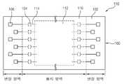
도 1a 및 도 1b는 본 발명의 실시예에 따른 인쇄회로기판을 도시한 도면이고, 도 2a 및 도 2b는 본 발명의 실시예에 따른 인쇄회로기판을 이용한 반도체 패키지를 도시한 도면이며, 도 3a 내지 도 3c는 본 발명의 실시예에 따른 인쇄회로기판을 이용한 멀티 패키지를 도시한 도면이다.1A and 1B illustrate a printed circuit board according to an exemplary embodiment of the present invention, and FIGS. 2A and 2B illustrate a semiconductor package using a printed circuit board according to an exemplary embodiment of the present invention, and FIG. 3A. 3C is a diagram illustrating a multi-package using a printed circuit board according to an exemplary embodiment of the present invention.
도 1a 및 도 1b를 참조하면, 본 발명에 따른 인쇄회로기판(100)은 봉지 영역 및 상기 봉지 영역의 외측으로 연장된 연장 영역을 갖는 절연층(102)을 포함하여 이루어진다. 상기 절연층(102)의 봉지 영역 일면에는 다수의 전극 단자(104)가 구비되고, 상기 절연층(102)의 연장 영역에는 상기 봉지 영역의 전극 단자(104)와 전기적으로 연결되는 제1연결단자(106)가 구비되며, 상기 절연층(102)의 타면에는 다수의 볼랜드를 포함하는 제2연결단자(108)가 형성된다.1A and 1B, the printed
상기 인쇄회로기판(100)은 다양한 형태의 반도체 패키지 및 스택 패키지를 포함하는 멀티 패키지를 형성하기 위하여 절곡과 같은 형태의 변경이 가능한 플렉서블(Flexible) 기판이다.The printed
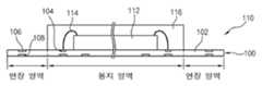
상기 인쇄회로기판을 이용하여 형성된 반도체 패키지는 도 2a 내지 도 2b에 도시된 바와 같다.The semiconductor package formed using the printed circuit board is as shown in FIGS. 2A to 2B.
도 2a 및 도 2b를 참조하면, 본 발명에 따른 반도체 패키지(110)는 상기 도 1a 내지 도 1b에 도시된 인쇄회로기판(100)과 반도체 칩(112) 및 봉지부(116)를 포함하여 이루어진다.2A and 2B, the
상기 반도체 칩(112)은 상기 인쇄회로기판(100)의 봉지 영역 내에 적어도 하나 이상 배치되며, 상기 반도체 칩(112)는 상기 인쇄회로기판(100)의 봉지 영역에 형성된 전극 단자(104)와 금속와이어(114)와 같은 연결 매개를 통해 전기적으로 연결된다. 상기 인쇄회로기판(100)의 봉지 영역 상부에는 상기 반도체 칩을 덮도록 봉지부(116)가 형성된다.At least one
상기 반도체 칩(112)과 상기 인쇄회로기판(100)은 상기 금속와이어(114) 외에 플립 칩 패키지와 같은 다른 방법을 통하여 전기적으로 연결될 수 있다.The
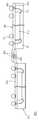
한편, 상기 도 2a 내지 도 2b에 도시된 본 발명에 따른 반도체 패키지를 이용하여 도 3a에 도시된 바와 같이 수직으로 스택된 형태의 멀티 패키지를 형성할 수 있으며, 도 3b 및 도 3c에 도시된 바와 같이 수평으로 배열된 형태의 멀티 패키지를 형성할 수 있다.On the other hand, using the semiconductor package according to the present invention shown in Figures 2a to 2b can form a multi-package of the vertically stacked form as shown in Figure 3a, as shown in Figures 3b and 3c It is possible to form a multi-package of the horizontally arranged form.
도 3a를 참조하면, 본 발명에 따른 멀티 패키지(120)는 상기 도 2a 내지 도 2b의 반도체 패키지들이 수직으로 스택되어 이루어진다.Referring to FIG. 3A, the multi-package 120 according to the present invention is formed by vertically stacking the semiconductor packages of FIGS. 2A through 2B.
자세하게, 본 발명에 따른 반도체 패키지(110)들은 접착제(미도시)를 매개로 수직적으로 스택되며, 상기 각 반도체 패키지(110)의 봉지부(116) 외측 연장 영역은 절곡되어 상기 반도체 패키지(110)들의 측면에 배치된다.In detail, the
상기 스택된 반도체 패키지(110)들 중 하나의 반도체 패키지(110) 연장 영역의 제1 및 제2연결단자(106, 108)는 이에 대응하는 상기 하나의 반도체 패키지(110) 상부 및 하부에 배치되는 반도체 패키지(110) 연장 영역의 제1 및 제2연결단자(106, 108)와 접합되어 전기적으로 연결된다.The first and
상기 각 반도체 패키지(110)는 전기적인 연결을 위하여 연장 영역의 길이가 상호 다르게 형성될 수 있으며, 상기 각 반도체 패키지(110)의 연장 영역은 상기 각 반도체 패키지(110)의 다수면으로 연장될 수 있다.Each of the
상기 최하부에 스택된 반도체 패키지(110)의 제2연결단자(108)에는 솔더볼과 같은 외부접속단자(122)가 부착되며, 상기 스택된 반도체 패키지(110)들의 인쇄회로기판 부분을 보호하기 위하여 별도의 봉지부(미도시)가 형성될 수 있다.An
아울러, 본 발명에 따른 멀티 패키지(120)는, 도 3b 및 도 3c에 도시된 바와 같이, 다수의 반도체 패키지(110)가 수평으로 배치되고, 상기 각 반도체 패키지(110) 연장 영역의 제1 및 제2연결단자(106, 108)들이 상호 접합되어 전기적으로 연결된다.In addition, in the multi-package 120 according to the present invention, as illustrated in FIGS. 3B and 3C, a plurality of
자세하게, 도 3b에 도시된 바와 같이, 본 발명에 따른 멀티 패키지(120)는 상기 각 반도체 패키지(110)의 봉지부(116) 외측 연장 영역이 절곡되어 상기 각 반도체 패키지(110)의 제2연결단자(108)들이 상호 접합되어 전기적으로 연결되도록 이루어진다.In detail, as illustrated in FIG. 3B, in the multi-package 120 according to the present invention, an extension area outside the
또한, 도 3c에 도시된 바와 같이, 본 발명에 따른 멀티 패키지(120)는 상기 각 반도체 패키지(110)의 봉지부(116) 외측 연장 영역들이 상호 오버랩되어 하나의 반도체 패키지(110)의 제1연결단자(106)와 다른 하나의 반도체 패키지의 제2연결단자(108)가 상호 접합되어 전기적으로 연결되도록 이루어진다.In addition, as shown in FIG. 3C, the multi-package 120 according to the present invention overlaps the outer portions of the
상기 수평으로 배열된 각 반도체 패키지들의 제2연결단자에는 솔더볼과 같은 외부접속단자가 부착되며, 상기 각 반도체 패키지(110)의 연장 영역은 상기 각 반도체 패키지(110)의 다수면으로 연장될 수 있다.External connection terminals such as solder balls may be attached to the second connection terminals of the semiconductor packages arranged horizontally, and an extension region of each
상기 연장 영역을 갖는 인쇄회로기판을 이용하여 형성되는 멀티 패키지는 상기 인쇄회로기판의 연장 영역 형상에 따라 다양한 형태를 갖도록 전기적으로 연결될 수 있다.The multi-package formed using the printed circuit board having the extension area may be electrically connected to have various shapes according to the shape of the extension area of the printed circuit board.
이상에서와 같이, 본 발명은 봉지 영역의 외측으로 돌출되도록 연장 영역을 갖고 상기 연장 영역에 연결단자가 구비된 인쇄회로기판을 이용하여 반도체 패키지들을 형성하고, 상기 반도체 패키지의 연장 영역을 절곡하여 상호 전기적으로 연결되도록 멀티 패키지를 형성한다.As described above, the present invention forms a semiconductor package by using a printed circuit board having an extension region so as to protrude to the outside of the encapsulation region and the connection terminal is provided in the extension region, and by bending the extension region of the semiconductor package Form a multi-package to be electrically connected.
따라서, 전기적인 연결을 위하여 기판, 연결 핀 및 외부접속단자와 같은 별도의 매개물 없이 멀티 패키지를 형성함으로써 전체 멀티 패키지의 높이를 줄일 수 있다.Therefore, the height of the entire multi-package can be reduced by forming a multi-package without an additional medium such as a substrate, a connection pin and an external connection terminal for electrical connection.
또한, 멀티 패키지를 형성하기 위하여 별도의 매개물이 필요 없어 외부 충격에 의해 멀티 패키지의 데미지를 줄일 수 있으며, 멀티 패키지의 제조 비용을 감소시킬 수 있다.In addition, it is possible to reduce the damage of the multi-package due to an external impact, because it is not necessary to form a multi-package, it is possible to reduce the manufacturing cost of the multi-package.
이상, 여기에서는 본 발명을 특정 실시예에 관련하여 도시하고 설명하였지만, 본 발명이 그에 한정되는 것은 아니며, 이하의 특허청구의 범위는 본 발명의 정신과 분야를 이탈하지 않는 한도 내에서 본 발명이 다양하게 개조 및 변형될 수 있다는 것을 당업계에서 통상의 지식을 가진 자가 용이하게 알 수 있다.As mentioned above, although the present invention has been illustrated and described with reference to specific embodiments, the present invention is not limited thereto, and the following claims are not limited to the scope of the present invention without departing from the spirit and scope of the present invention. It can be easily understood by those skilled in the art that can be modified and modified.
102 ; 절연층 104 ; 전극 단자
106 ; 제1연결단자 108 ; 제2연결단자
110 ; 반도체 패키지 112 ; 반도체 칩
114 ; 금속와이어 116 ; 봉지부
120 ; 멀티 패키지102; Insulating
106;
110;
114;
120; Multi package
Claims (4)
Translated fromKorean상기 각 반도체 패키지 연장 영역의 상호 대응하는 제1 및 제2연결 단자들이 접합되어 전기적으로 연결된 것을 특징으로 하는 멀티 패키지.An insulating layer having an encapsulation area and an extension area extending outwardly of the encapsulation area, an electrode terminal formed on one surface of the encapsulation area of the insulating layer, and an extension layer formed in the insulating area and electrically connected to the electrode terminal of the encapsulation area. A substrate including a first connection terminal and a second connection terminal formed on the other surface of the insulating layer, at least one semiconductor chip attached in the encapsulation region of the substrate, and an encapsulation portion covering the encapsulation region to expose the extension region of the substrate. The semiconductor package is arranged in a plurality of horizontal,
The first and second connection terminals corresponding to each of the semiconductor package extension regions may be bonded to each other to be electrically connected to each other.
상기 기판은 플렉스블(Flexible) 기판인 것을 특징으로 하는 멀티 패키지.The method of claim 1,
The substrate is a multi-package, characterized in that the flexible (flexible) substrate.
상기 각 반도체 패키지의 연장 영역은 절곡된 것을 특징으로 하는 멀티 패키지.The method of claim 1,
The extension region of each semiconductor package is bent.
상기 각 반도체 패키지의 연장 영역은 상기 각 반도체 패키지의 다수면으로 연장된 것을 특징으로 하는 멀티 패키지.The method of claim 1,
The extended region of each semiconductor package is extended to a plurality of surfaces of each semiconductor package.
Priority Applications (1)
| Application Number | Priority Date | Filing Date | Title |
|---|---|---|---|
| KR1020110105160AKR101096457B1 (en) | 2011-10-14 | 2011-10-14 | Multi package |
Applications Claiming Priority (1)
| Application Number | Priority Date | Filing Date | Title |
|---|---|---|---|
| KR1020110105160AKR101096457B1 (en) | 2011-10-14 | 2011-10-14 | Multi package |
Related Parent Applications (1)
| Application Number | Title | Priority Date | Filing Date |
|---|---|---|---|
| KR1020110069385ADivisionKR101096456B1 (en) | 2011-07-13 | 2011-07-13 | Multi package |
Publications (2)
| Publication Number | Publication Date |
|---|---|
| KR20110118758A KR20110118758A (en) | 2011-11-01 |
| KR101096457B1true KR101096457B1 (en) | 2011-12-20 |
Family
ID=45390494
Family Applications (1)
| Application Number | Title | Priority Date | Filing Date |
|---|---|---|---|
| KR1020110105160AExpired - Fee RelatedKR101096457B1 (en) | 2011-10-14 | 2011-10-14 | Multi package |
Country Status (1)
| Country | Link |
|---|---|
| KR (1) | KR101096457B1 (en) |
Citations (1)
| Publication number | Priority date | Publication date | Assignee | Title |
|---|---|---|---|---|
| KR100287805B1 (en) | 1997-08-11 | 2001-04-16 | 다니구찌 이찌로오, 기타오카 다카시 | Semiconductor component |
- 2011
- 2011-10-14KRKR1020110105160Apatent/KR101096457B1/ennot_activeExpired - Fee Related
Patent Citations (1)
| Publication number | Priority date | Publication date | Assignee | Title |
|---|---|---|---|---|
| KR100287805B1 (en) | 1997-08-11 | 2001-04-16 | 다니구찌 이찌로오, 기타오카 다카시 | Semiconductor component |
Also Published As
| Publication number | Publication date |
|---|---|
| KR20110118758A (en) | 2011-11-01 |
Similar Documents
| Publication | Publication Date | Title |
|---|---|---|
| CN108022923B (en) | Semiconductor package | |
| KR100753415B1 (en) | Stack package | |
| KR101454884B1 (en) | A package system that is a stacked integrated circuit package | |
| KR101070913B1 (en) | Stacked die package | |
| KR20240168899A (en) | Semiconductor package | |
| KR20180046990A (en) | Semiconductor packages of asymmetric chip stacks | |
| KR20110078399A (en) | Stack Package and Manufacturing Method Thereof | |
| KR101544508B1 (en) | Printed circuit board and semiconductor package having bond fingers | |
| KR20110124065A (en) | Stacked Semiconductor Packages | |
| CN107293520A (en) | Stacked type semiconductor package part | |
| KR101219484B1 (en) | Semiconductor chip module and semiconductor package having the same and package module | |
| CN103400826B (en) | Semiconductor packages and manufacture method thereof | |
| KR20100050976A (en) | Semiconductor package and method for fabricating the same | |
| KR101219086B1 (en) | Package module | |
| KR101096457B1 (en) | Multi package | |
| KR101096456B1 (en) | Multi package | |
| KR20090096181A (en) | Stack package | |
| KR20100050981A (en) | Semiconductor package and stack package using the same | |
| KR20090096176A (en) | Printed circuit board and semiconductor package and multi package using the same | |
| KR101332873B1 (en) | Interposer for providing capacitance and lead frame type semiconductor package using the same | |
| KR102029804B1 (en) | Package on package type semiconductor package and manufacturing method thereof | |
| KR20110130017A (en) | Multi-chip package and manufacturing method thereof | |
| KR20080061604A (en) | Multichip Package | |
| KR101207883B1 (en) | package module | |
| KR101019705B1 (en) | Substrate for manufacturing semiconductor package and semiconductor package using same |
Legal Events
| Date | Code | Title | Description |
|---|---|---|---|
| A107 | Divisional application of patent | ||
| A201 | Request for examination | ||
| PA0107 | Divisional application | St.27 status event code:A-0-1-A10-A16-div-PA0107 St.27 status event code:A-0-1-A10-A18-div-PA0107 | |
| PA0201 | Request for examination | St.27 status event code:A-1-2-D10-D11-exm-PA0201 | |
| PG1501 | Laying open of application | St.27 status event code:A-1-1-Q10-Q12-nap-PG1501 | |
| E701 | Decision to grant or registration of patent right | ||
| PE0701 | Decision of registration | St.27 status event code:A-1-2-D10-D22-exm-PE0701 | |
| GRNT | Written decision to grant | ||
| PR0701 | Registration of establishment | St.27 status event code:A-2-4-F10-F11-exm-PR0701 | |
| PR1002 | Payment of registration fee | Fee payment year number:1 St.27 status event code:A-2-2-U10-U11-oth-PR1002 | |
| PG1601 | Publication of registration | St.27 status event code:A-4-4-Q10-Q13-nap-PG1601 | |
| PN2301 | Change of applicant | St.27 status event code:A-5-5-R10-R11-asn-PN2301 St.27 status event code:A-5-5-R10-R13-asn-PN2301 | |
| PN2301 | Change of applicant | St.27 status event code:A-5-5-R10-R11-asn-PN2301 St.27 status event code:A-5-5-R10-R13-asn-PN2301 | |
| LAPS | Lapse due to unpaid annual fee | ||
| PC1903 | Unpaid annual fee | Not in force date:20141215 Payment event data comment text:Termination Category : DEFAULT_OF_REGISTRATION_FEE St.27 status event code:A-4-4-U10-U13-oth-PC1903 | |
| PN2301 | Change of applicant | St.27 status event code:A-5-5-R10-R11-asn-PN2301 St.27 status event code:A-5-5-R10-R13-asn-PN2301 | |
| PC1903 | Unpaid annual fee | Ip right cessation event data comment text:Termination Category : DEFAULT_OF_REGISTRATION_FEE Not in force date:20141215 St.27 status event code:N-4-6-H10-H13-oth-PC1903 |