KR101095739B1 - Semiconductor element and method of forming the same - Google Patents
Semiconductor element and method of forming the sameDownload PDFInfo
- Publication number
- KR101095739B1 KR101095739B1KR1020100130008AKR20100130008AKR101095739B1KR 101095739 B1KR101095739 B1KR 101095739B1KR 1020100130008 AKR1020100130008 AKR 1020100130008AKR 20100130008 AKR20100130008 AKR 20100130008AKR 101095739 B1KR101095739 B1KR 101095739B1
- Authority
- KR
- South Korea
- Prior art keywords
- forming
- bit line
- gate
- contact plug
- layer
- Prior art date
- Legal status (The legal status is an assumption and is not a legal conclusion. Google has not performed a legal analysis and makes no representation as to the accuracy of the status listed.)
- Expired - Fee Related
Links
Images


Classifications
- H—ELECTRICITY
- H10—SEMICONDUCTOR DEVICES; ELECTRIC SOLID-STATE DEVICES NOT OTHERWISE PROVIDED FOR
- H10B—ELECTRONIC MEMORY DEVICES
- H10B12/00—Dynamic random access memory [DRAM] devices
- H10B12/01—Manufacture or treatment
- H10B12/02—Manufacture or treatment for one transistor one-capacitor [1T-1C] memory cells
- H10B12/05—Making the transistor
- H10B12/053—Making the transistor the transistor being at least partially in a trench in the substrate
- H—ELECTRICITY
- H10—SEMICONDUCTOR DEVICES; ELECTRIC SOLID-STATE DEVICES NOT OTHERWISE PROVIDED FOR
- H10B—ELECTRONIC MEMORY DEVICES
- H10B12/00—Dynamic random access memory [DRAM] devices
- H10B12/01—Manufacture or treatment
- H10B12/09—Manufacture or treatment with simultaneous manufacture of the peripheral circuit region and memory cells
- H—ELECTRICITY
- H10—SEMICONDUCTOR DEVICES; ELECTRIC SOLID-STATE DEVICES NOT OTHERWISE PROVIDED FOR
- H10D—INORGANIC ELECTRIC SEMICONDUCTOR DEVICES
- H10D64/00—Electrodes of devices having potential barriers
- H10D64/01—Manufacture or treatment
- H10D64/017—Manufacture or treatment using dummy gates in processes wherein at least parts of the final gates are self-aligned to the dummy gates, i.e. replacement gate processes
Landscapes
- Engineering & Computer Science (AREA)
- Manufacturing & Machinery (AREA)
- Semiconductor Memories (AREA)
Abstract
Translated fromKoreanDescription
Translated fromKorean본 발명은 반도체 소자 및 그 형성 방법에 관한 것으로, 보다 자세하게는 매립형 게이트의 저장전극 콘택플러그를 포함하는 반도체 소자 및 그 형성 방법에 관한 것이다.The present invention relates to a semiconductor device and a method of forming the same, and more particularly, to a semiconductor device including a storage electrode contact plug of a buried gate and a method of forming the same.
최근 대부분의 전자 제품들(electronic appliances)은 반도체 소자(semiconductor devices)를 구비한다. 상기 반도체 소자는 트랜지스터, 저항 및 커패시터 등의 전자 부품(electronic element)들을 구비하며, 이들 전자 부품들은 상기 전자 제품들의 부분적 기능을 수행할 수 있도록 설계된 후, 반도체 기판 상에 집적된다. 예를 들면, 컴퓨터 또는 디지털 카메라 등의 전자 제품들은 정보 저장을 위한 메모리 칩(memory chip), 정보 제어를 위한 처리 칩(processing chip) 등의 반도체 장치들을 구비하고, 상기 메모리 칩 및 처리 칩은 반도체 기판 상에 집적된 상기 전자 부품들을 구비한다.Recently, most electronic appliances have semiconductor devices. The semiconductor device includes electronic elements such as transistors, resistors, and capacitors, which are designed to perform partial functions of the electronic products and then integrated on the semiconductor substrate. For example, electronic products such as a computer or a digital camera include semiconductor devices such as a memory chip for storing information and a processing chip for controlling information, and the memory chip and the processing chip are semiconductors. And the electronic components integrated on a substrate.
한편, 반도체 소자들은 소비자가 요구하는 우수한 성능 및 저렴한 가격을 충족시키기 위해 점점 더 고집적화될 필요가 있다. 반도체 소자의 집적도가 높아지면서 디자인 룰(design rule)이 감소하게 되어 반도체 소자의 패턴도 미세화되고 있다. 반도체 소자의 극미세화 및 고집적화가 진행됨에 따라 메모리 용량의 증가에 비례하여 전체적인 칩(chip) 면적은 증가되고 있지만 실제로 반도체 소자의 패턴이 형성되는 셀(cell) 영역의 면적은 감소되고 있다. 따라서, 원하는 메모리 용량을 확보하기 위해서는 한정된 셀 영역 내에 보다 많은 패턴이 형성되어야만 하므로, 패턴의 선폭(critical dimension)이 감소된 미세 패턴을 형성하여야 한다.On the other hand, semiconductor devices need to be increasingly integrated to meet consumer demands for superior performance and low cost. As the degree of integration of semiconductor devices increases, the number of design rules decreases and the pattern of semiconductor devices becomes finer. As miniaturization and high integration of a semiconductor device progresses, the overall chip area increases in proportion to an increase in memory capacity, but the area of a cell area where a semiconductor device pattern is formed is actually decreasing. Therefore, in order to secure a desired memory capacity, more patterns must be formed in a limited cell region, so that a fine pattern with a reduced critical dimension of the pattern must be formed.
반도체 소자의 종류 중에서 디램(DRAM)은 캐패시터 및 트랜지스터로 구성된 단위 셀(unit cell)을 다수 포함하고 있다. 이 중 캐패시터는 데이터를 임시 저장하기 위해 사용되고, 트랜지스터는 환경에 따라 전기 전도도가 변화하는 반도체의 성질을 이용하여 제어 신호(워드 라인)에 대응하여 비트라인과 캐패시터 간 데이터를 전달하기 위해 사용된다. 트랜지스터는 게이트(gate), 소스(source) 및 드레인(drain)의 세 영역으로 구성되어 있다. 게이트로 입력되는 제어 신호에 따라 소스와 드레인 간 전하의 이동이 일어난다. 소스와 드레인 간 전하의 이동은 채널(channel) 영역을 통해 이루어지는데 바로 이 채널이 반도체의 성질을 이용한 것이다.Among the types of semiconductor devices, a DRAM includes a plurality of unit cells including capacitors and transistors. Among them, a capacitor is used for temporarily storing data, and a transistor is used for transferring data between a bit line and a capacitor corresponding to a control signal (word line) by using the property of a semiconductor whose electrical conductivity changes according to an environment. A transistor consists of three regions: a gate, a source, and a drain. A charge is transferred between the source and the drain in accordance with a control signal input to the gate. The transfer of charge between the source and drain occurs through the channel region, which uses the nature of the semiconductor.
반도체 기판에 통상적인 트랜지스터를 만드는 경우 반도체 기판에 게이트를 형성하고 게이트의 양 옆에 불순물을 도핑하여 소스와 드레인을 형성해 왔다. 이 경우 게이트 아래 소스와 드레인 사이가 트랜지스터의 채널 영역이 된다. 이러한 수평 채널 영역을 가지는 트랜지스터는 일정 면적의 반도체 기판을 차지하고 있다. 복잡한 반도체 기억 장치의 경우 내부에 포함된 다수의 트랜지스터로 인하여 전체 면적을 줄이는 데 어려움이 발생한다.When a conventional transistor is formed on a semiconductor substrate, a gate is formed on a semiconductor substrate and doping is performed on both sides of the gate to form a source and a drain. In this case, the region between the source and the drain under the gate becomes the channel region of the transistor. A transistor having such a horizontal channel region occupies a semiconductor substrate of a certain area. In the case of a complicated semiconductor memory device, it is difficult to reduce the total area due to a plurality of transistors included in the semiconductor memory device.
반도체 기억 장치의 전체 면적을 줄이면 하나의 웨이퍼 당 생산 가능한 반도체 기억 장치의 수를 증가시킬 수 있어 생산성이 향상된다. 반도체 기억 장치의 전체 면적을 줄이기 위해 여러 가지 방법들이 제안되고 있다. 이 중 하나가 수평 채널 영역을 가지던 종래의 플래너 게이트(Planar Gate)를 대신하여, 기판에 리세스가 형성되고 그 리세스에 게이트를 형성함으로써 리세스의 곡면을 따라 채널 영역이 형성되는 리세스 게이트를 사용하는 것이며, 이 리세스 게이트에서 나아가 리세스 내에 게이트 전체를 매립하여 형성하는 매립형 게이트(Buried Gate)가 연구되고 있다.By reducing the total area of the semiconductor memory device, the number of semiconductor memory devices that can be produced per wafer can be increased and productivity is improved. Various methods have been proposed to reduce the total area of the semiconductor memory device. In place of a conventional planar gate in which one of them has a horizontal channel region, a recess is formed in the substrate and a gate is formed in the recess, thereby forming a recess in which the channel region is formed along the curved surface of the recess A buried gate is formed by embedding the entire gate in the recess in addition to the recessed gate.
매립형 게이트를 포함하는 반도체 소자에서 비트라인 콘택플러그는 매립형 게이트가 구비되어 있는 반도체 기판의 활성영역과 접속된다. 일반적인 비트라인 콘택플러그의 형성 방법을 간략히 살펴보면 다음과 같다.In a semiconductor device including a buried gate, the bit line contact plug is connected to an active region of a semiconductor substrate having a buried gate. A brief description will be given of a general method of forming a bit line contact plug.
매립형 게이트가 구비되어 있는 반도체 기판 상에 층간절연막을 형성한 후, 활성영역이 노출되도록 층간절연막을 식각하여 비트라인 콘택홀을 형성한다. 이때, 비트라인 콘택홀의 하부는 활성영역이 충분히 덮어지는 크기를 갖도록 한다. 이어서 비트라인 콘택홀의 측벽에 스페이서를 형성하고 비트라인 콘택홀을 매립하는 비트라인 콘택플러그를 형성하는데, 여기서 비트라인 콘택플러그는 스페이서에 의해 하부보다 상부의 폭이 넓어져 후속 공정에서 형성되는 저장전극 콘택플러그의 마진을 감소시켜 저장전극 콘택플러그 영역을 오픈시키지 않아 활성영역과 정확하게 접속되지 않는 문제를 발생시켜 반도체 소자의 특성을 저하시킨다.After forming the interlayer dielectric layer on the semiconductor substrate including the buried gate, the interlayer dielectric layer is etched to expose the active region, thereby forming bit line contact holes. At this time, the lower portion of the bit line contact hole has a size that sufficiently covers the active region. Subsequently, a spacer is formed on the sidewall of the bit line contact hole and a bit line contact plug is formed to fill the bit line contact hole, wherein the bit line contact plug has a width wider than the lower portion by the spacer and is formed in a subsequent process. The margin of the contact plug is reduced so that the storage electrode contact plug region is not opened, thereby causing a problem of not being accurately connected to the active region, thereby degrading the characteristics of the semiconductor device.
본 발명은 매립형 게이트를 포함하는 반도체 소자에서 저장전극 콘택플러그를 형성하는데 공정 마진이 감소하여 오픈되지 않는 문제를 해결하고자 한다.An object of the present invention is to solve a problem in that a process margin is reduced in forming a storage electrode contact plug in a semiconductor device including a buried gate and is not opened.
본 발명의 반도체 소자는 셀 영역 및 주변회로 영역을 포함하고, 소자분리막으로 정의되는 활성영역을 포함하는 반도체 기판과, 상기 활성영역의 상부에 구비되며 상기 활성영역의 중앙부 및 양단부를 노출시키는 더미 게이트, 상기 더미 게이트 사이에 구비되며 상기 활성영역의 중앙부와 연결되는 비트라인 콘택플러그와, 상기 더미 게이트에 의해 상기 비트라인 콘택플러그와 이격되며 상기 활성영역의 양단부와 연결되는 저장전극 콘택플러그를 포함하는 것을 특징으로 한다.The semiconductor device of the present invention includes a semiconductor substrate including a cell region and a peripheral circuit region, and includes an active region defined as an isolation layer, and a dummy gate disposed on the active region and exposing a central portion and both ends of the active region. And a bit line contact plug provided between the dummy gates and connected to a central portion of the active region, and a storage electrode contact plug spaced apart from the bit line contact plug by the dummy gate and connected to both ends of the active region. It is characterized by.
그리고, 상기 더미 게이트는 절연막을 포함하는 것을 특징으로 한다.The dummy gate may include an insulating film.
그리고, 상기 셀 영역 내에 매립된 매립형 게이트를 더 포함하는 것을 특징으로 한다.And a buried gate embedded in the cell region.
그리고, 상기 비트라인 콘택플러그를 둘러싸는 스페이서를 더 포함하는 것을 특징으로 한다.The apparatus may further include a spacer surrounding the bit line contact plug.
그리고, 상기 비트라인 콘택플러그 상부와 연결되며, 상기 더미 게이트와 평행하는 비트라인을 더 포함하는 것을 특징으로 한다.And a bit line connected to an upper portion of the bit line contact plug and parallel to the dummy gate.
그리고, 상기 비트라인 콘택플러그, 상기 저장전극 콘택플러그 및 상기 더미 게이트의 사이를 매립하는 층간절연막을 더 포함하는 것을 특징으로 한다.And an interlayer insulating layer filling the bit line contact plug, the storage electrode contact plug, and the dummy gate.
그리고, 상기 주변회로 영역의 상기 반도체 기판 상부에 구비된 동작 게이트를 더 포함하는 것을 특징으로 한다.In addition, the semiconductor device may further include an operation gate provided on the semiconductor substrate in the peripheral circuit region.
그리고, 상기 더미 게이트는 상기 동작 게이트와 동일한 높이를 갖는 것을 특징으로 한다.The dummy gate may have the same height as the operation gate.
본 발명의 반도체 소자의 형성 방법은 셀 영역 및 주변회로 영역을 포함하고, 소자분리막으로 정의되는 활성영역을 포함하는 반도체 기판 상부에 상기 활성영역의 중앙부 및 양단부를 노출시키는 더미 게이트를 형성하는 단계와, 상기 더미 게이트 사이에 상기 활성영역의 중앙부와 연결되는 비트라인 콘택플러그를 형성하는 단계와, 상기 더미 게이트에 의해 상기 비트라인 콘택플러그와 이격되며 상기 활성영역의 양단부와 연결되는 저장전극 콘택플러그를 형성하는 단계를 포함하는 것을 특징으로 한다.A method of forming a semiconductor device of the present invention includes forming a dummy gate on a semiconductor substrate including a cell region and a peripheral circuit region and exposing a central portion and both ends of the active region on an upper portion of a semiconductor substrate including an active region defined as an isolation layer; Forming a bit line contact plug between the dummy gate and the center line of the active region, and a storage electrode contact plug spaced apart from the bit line contact plug by the dummy gate and connected to both ends of the active region. It characterized by comprising the step of forming.
그리고, 상기 더미 게이트를 형성하는 단계 이전 상기 셀 영역의 상기 반도체 기판 내에 매립되는 매립형 게이트를 형성하는 단계를 더 포함하는 것을 특징으로 한다.The method may further include forming a buried gate embedded in the semiconductor substrate in the cell region before forming the dummy gate.
그리고, 상기 매립형 게이트를 형성하는 단계 이후 상기 주변회로 영역에 게이트 산화막을 형성하는 단계와, 상기 게이트 산화막 상부에 폴리실리콘층을 형성하는 단계와, 상기 폴리실리콘층 상부에 배리어 도전층을 형성하는 단계와, 상기 배리어 도전층 상부에 게이트 금속층을 형성하는 단계를 더 포함하는 것을 특징으로 한다.And forming a gate oxide layer in the peripheral circuit region after forming the buried gate, forming a polysilicon layer on the gate oxide layer, and forming a barrier conductive layer on the polysilicon layer. And forming a gate metal layer on the barrier conductive layer.
그리고, 상기 배리어 도전층을 형성하는 단계 이후 상기 셀 영역의 상기 반도체 기판 및 상기 주변회로 영역의 상기 게이트 금속층 상부에 하드마스크층을 형성하는 단계를 더 포함하는 것을 특징으로 한다.And forming a hard mask layer on the semiconductor substrate of the cell region and the gate metal layer of the peripheral circuit region after forming the barrier conductive layer.
그리고, 상기 더미 게이트를 형성하는 단계는 상기 하드마스크층 상부에 마스크 패턴을 형성하는 단계와, 상기 마스크 패턴을 식각마스크로 상기 활성영역의 중앙부 및 상기 활성영역의 양단부가 노출되도록 상기 셀 영역의 하드마스크층을 식각하는 단계를 포함하는 것을 특징으로 한다.The forming of the dummy gate may include forming a mask pattern on the hard mask layer, and hardening the cell region so that the center portion of the active region and both ends of the active region are exposed using the mask pattern as an etch mask. And etching the mask layer.
그리고, 상기 더미 게이트를 형성하는 단계와 동시에 상기 마스크 패턴을 식각마스크로 상기 주변회로 영역의 상기 하드마스크층, 상기 폴리실리콘층, 상기 배리어 도전층 및 상기 게이트 금속층을 식각하여 동작 게이트를 형성하는 것을 특징으로 한다.And simultaneously forming the dummy gate by etching the hard mask layer, the polysilicon layer, the barrier conductive layer, and the gate metal layer in the peripheral circuit region using the mask pattern as an etch mask. It features.
그리고, 상기 동작 게이트를 형성하는 단계 이후 상기 셀 영역의 반도체 기판 및 상기 주변회로 영역의 동작 게이트 측벽에 스페이서 절연막을 형성하는 단계를 더 포함하는 것을 특징으로 한다.The method may further include forming a spacer insulating layer on sidewalls of the semiconductor substrate of the cell region and the operation gate of the peripheral circuit region after the forming of the operation gate.
그리고, 상기 동작 게이트를 형성하는 단계 이후 상기 더미 게이트 및 상기 동작 게이트 사이가 매립되도록 상기 셀 영역 및 상기 주변회로 영역에 층간절연막을 형성하는 단계를 더 포함하는 것을 특징으로 한다.And forming an interlayer insulating film in the cell region and the peripheral circuit region to fill the gap between the dummy gate and the operation gate after the forming of the operation gate.
그리고, 상기 비트라인 콘택플러그를 형성하는 단계는 상기 층간절연막 상부에 비트라인 콘택홀을 정의하는 마스크 패턴을 형성하는 단계와, 상기 마스크 패턴을 식각마스크로 상기 활성영역의 중앙부가 노출되도록 상기 층간절연막을 식각하여 비트라인 콘택홀을 형성하는 단계와, 상기 비트라인 콘택홀이 매립되도록 도전층을 형성하는 단계를 포함하는 것을 특징으로 한다.The forming of the bit line contact plug may include forming a mask pattern defining a bit line contact hole on the interlayer insulating layer and exposing the center portion of the active region with the mask pattern as an etch mask. Etching to form a bit line contact hole, and forming a conductive layer to fill the bit line contact hole.
그리고, 상기 비트라인 콘택홀을 형성하는 단계는 상기 더미 게이트와의 식각선택비를 이용하여 상기 층간절연막을 식각하는 것을 특징으로 한다.In the forming of the bit line contact hole, the interlayer dielectric layer may be etched using an etch selectivity with the dummy gate.
그리고, 상기 비트라인 콘택플러그를 형성하는 단계 이전 상기 비트라인 콘택홀 내부에 스페이서를 형성하는 단계를 더 포함하는 것을 특징으로 한다.The method may further include forming a spacer in the bit line contact hole before forming the bit line contact plug.
그리고, 상기 저장전극 콘택플러그를 형성하는 단계는 상기 층간절연막 상부에 저장전극 콘택홀을 정의하는 마스크 패턴을 형성하는 단계와, 상기 마스크 패턴을 식각마스크로 상기 활성영역의 양단부가 노출되도록 상기 층간절연막을 식각하여 저장전극 콘택홀을 형성하는 단계와, 상기 저장전극 콘택홀이 매립되도록 도전층을 형성하는 단계를 포함하는 것을 특징으로 한다.The forming of the storage electrode contact plug may include forming a mask pattern defining a storage electrode contact hole on the interlayer insulating layer, and exposing both ends of the active region with the mask pattern as an etch mask. Etching to form a storage electrode contact hole, and forming a conductive layer to fill the storage electrode contact hole.
그리고, 상기 저장전극 콘택홀을 형성하는 단계는 상기 더미 게이트와의 자기정렬방식으로 수행되는 것을 특징으로 한다.The forming of the storage electrode contact hole may be performed by a self-alignment method with the dummy gate.
그리고, 상기 저장전극 콘택플러그를 형성하는 단계 이후, 상기 비트라인 콘택플러그 상부와 연결되며 상기 더미 게이트와 평행하는 비트라인을 형성하는 단계를 더 포함하는 것을 특징으로 한다.The method may further include forming a bit line connected to an upper portion of the bit line contact plug and parallel to the dummy gate after forming the storage electrode contact plug.
본 발명은 매립형 게이트를 포함하는 반도체 소자에서 저장전극 콘택홀이 오픈되지 않는 문제를 근본적으로 해결하여 반도체 소자의 특성을 향상시킬 수 있는 효과를 제공한다.The present invention fundamentally solves the problem that the storage electrode contact hole is not opened in a semiconductor device including a buried gate, thereby providing an effect of improving the characteristics of the semiconductor device.
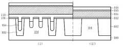
도 1은 본 발명에 따른 반도체 소자를 나타낸 것으로, (ⅰ)은 셀 영역을 나타낸 단면도이고, (ⅱ)는 주변회로 영역을 나타낸 단면도이고, (ⅲ)은 셀 영역을 나타낸 평면도.
도 2a 내지 도 2l은 본 발명에 따른 반도체 소자의 형성 방법을 나타낸 것으로, (ⅰ)은 셀 영역을 나타낸 단면도이고,(ⅱ)는 주변회로 영역을 나타낸 단면도이고, (ⅲ)은 셀 영역을 나타낸 평면도.1 shows a semiconductor device according to the present invention, (i) is a cross-sectional view showing a cell region, (ii) is a cross-sectional view showing a peripheral circuit region, and (i) is a plan view showing a cell region.
2A to 2L show a method of forming a semiconductor device according to the present invention, (i) is a sectional view showing a cell region, (ii) is a sectional view showing a peripheral circuit region, and (iii) a cell region. Floor plan.
이하에서는 본 발명의 실시예에 따라 첨부된 도면을 참조하여 상세히 설명하기로 한다.Hereinafter, with reference to the accompanying drawings in accordance with an embodiment of the present invention will be described in detail.
도 1은 본 발명에 따른 반도체 소자를 나타낸 것으로, (ⅰ)은 셀 영역을 나타낸 단면도이고, (ⅱ)는 주변회로 영역을 나타낸 단면도이고, (ⅲ)은 셀 영역을 나타낸 평면도이다.1 shows a semiconductor device according to the present invention, (i) is a cross-sectional view showing a cell region, (ii) is a cross-sectional view showing a peripheral circuit region, and (i) is a plan view showing a cell region.
도 1에 도시된 바와 같이, 본 발명의 반도체 소자는 셀 영역(ⅰ) 및 주변회로 영역(ⅱ)을 포함하고, 소자분리막(102)으로 정의되는 활성영역(104)을 포함하는 반도체 기판(100)과, 셀 영역(ⅰ)에 구비되며 상기 활성영역(104)의 중앙부 및 양단부를 노출시키는 섬 타입의 더미 게이트(122D)와, 주변회로 영역(ⅱ)에 구비되는 동작 게이트(122R)와, 더미 게이트(122D) 사이에 구비되며 활성영역(104)의 중앙부와 연결되는 비트라인 콘택플러그(132)와, 더미 게이트(122D)에 의해 비트라인 콘택플러그(132)와 이격되며 활성영역(104)의 상부와 연결되는 저장전극 콘택플러그(134)를 포함한다.As shown in FIG. 1, the semiconductor device of the present invention includes a
또한, 셀 영역(ⅰ) 내 매립된 매립형 게이트(108) 및 실링 절연막(110)을 더 포함하고, 비트라인 콘택플러그(132) 상부와 연결되며 더미 게이트(122D)와 평행하는 비트라인(138)을 더 포함하며, 비트라인 콘택플러그(132), 저장전극 콘택플러그(134) 및 더미 게이트(122D)를 이격시키는 층간절연막(126)을 더 포함하는 것이 바람직하다.The semiconductor device may further include a buried
그리고, 주변회로 영역(ⅱ)의 반도체 기판(100) 상에 동작 게이트(122R)를 더 포함하는 것이 바람직하고, 더미 게이트(122D)는 동작 게이트(122R)와 동일한 높이를 갖는 것이 바람직하다. 여기서, 더미 게이트(122D)는 전극층을 포함하지 않고 하드마스크층으로만 형성되기 때문에 비트라인 콘택플러그(132)가 저장전극 콘택플러그(134)와 쇼트되는 불량을 근본적으로 방지할 수 있다.In addition, it is preferable to further include an
상술한 바와 같이, 본 발명은 저장전극 콘택플러그가 셀 영역에 형성된 더 미 게이트에 의해 이격되도록 함으로써 저장전극 콘택플러그 형성 시 비트라인과의 자기정렬 페일 없이 저장전극 콘택플러그 영역의 마진을 향상시켜 저장전극 콘택플러그가 오픈되지 않는 문제를 근본적으로 해결할 수 있다.As described above, the present invention allows the storage electrode contact plugs to be spaced apart by a dummy gate formed in the cell region, thereby improving the storage electrode contact plug region margin without storing a self-aligning fail with the bit line when the storage electrode contact plug is formed. The problem that the electrode contact plug does not open can be fundamentally solved.
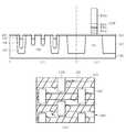
도 2a 내지 도 2l은 본 발명에 따른 반도체 소자의 형성 방법을 나타낸 것으로, (ⅰ)은 셀 영역을 나타낸 단면도이고,(ⅱ)는 주변회로 영역을 나타낸 단면도이고, (ⅲ)은 셀 영역을 나타낸 평면도이다.2A to 2L show a method of forming a semiconductor device according to the present invention, (i) is a sectional view showing a cell region, (ii) is a sectional view showing a peripheral circuit region, and (iii) a cell region. Top view.
도 2a에 도시된 바와 같이, 셀 영역(ⅰ) 및 주변회로 영역(ⅱ)을 포함하고, 소자분리막(102)에 의해 정의되는 활성영역(104)을 포함하는 반도체 기판(100) 상에 셀 영역(ⅰ)의 트렌치를 정의하기 위한 하드마스크 패턴(106)을 형성한다. 여기서 트렌치는 셀 영역(ⅰ)에만 형성되기 때문에 주변회로 영역(ⅱ)은 전체를 덮도록 형성하는 것이 바람직하다.As shown in FIG. 2A, a cell region on a
이어서, 하드마스크 패턴(106)을 마스크로 셀 영역(ⅰ)의 소자분리막(102) 및 활성영역(104)을 식각하여 트렌치를 형성한다. 그리고 트렌치 저부가 매립되도록 전극층을 형성하여 매립형 게이트(108)를 형성한 후, 매립형 게이트(108)를 포함하는 하드마스크 패턴(106) 상부에 실링 절연막(110)을 형성한다. 여기서 실링 절연막(110)은 질화막을 포함하는 것이 바람직하다.Next, the trench is formed by etching the
도 2b에 도시된 바와 같이, 주변회로 영역(ⅱ)을 오픈시키는 마스크(미도시)를 셀 영역(ⅰ) 상부에 형성하고, 이를 마스크로 주변회로 영역(ⅱ)의 반도체 기판(100)이 노출되도록 주변회로 영역(ⅱ)에 형성된 실링 절연막(110) 및 하드마스크 패턴(106)을 제거한다.As shown in FIG. 2B, a mask (not shown) for opening the peripheral circuit region ii is formed over the cell region, and the
도 2c에 도시된 바와 같이, 주변회로 영역(ⅱ)의 반도체 기판(100)을 산화시켜 게이트 산화막(112)을 형성한 후, 셀 영역(ⅰ)의 실링 절연막(110) 및 주변회로 영역(ⅱ)의 게이트 산화막(112) 상부에 폴리실리콘층(114), 배리어 도전층(116) 및 게이트 전극층(118)을 형성한다. 여기서 배리어 도전층(116)은 티타늄 또는 티타늄질화막을 포함하는 것이 바람직하고, 게이트 전극층(118)은 텅스텐을 포함하는 것이 바람직하다.As shown in FIG. 2C, after the
도 2d에 도시된 바와 같이, 셀 영역(ⅰ)을 오픈시키는 마스크(미도시)를 주변회로 영역(ⅱ) 상부에 형성하고, 이를 마스크로 셀 영역(ⅰ)의 실링절연막(110)이 노출되도록 게이트 전극층(118), 배리어 도전층(116) 및 폴리실리콘층(114)을 제거한다. 이때, 셀 영역(ⅰ)을 오픈시키는 마스크를 이용하여 게이트 전극층(118), 배리어 도전층(116) 및 폴리실리콘층(114)을 제거하는 것은 이들을 패터닝하여 비트라인을 형성하지 않기 위함이다. 이와 같이 비트라인을 의도적으로 형성하지 않는 점에 대해서는 도 2f에서 후술한다.As shown in FIG. 2D, a mask (not shown) for opening the cell region is formed over the peripheral circuit region ii, and the sealing insulating
도 2e에 도시된 바와 같이, 셀 영역(ⅰ)의 실링 절연막(110) 및 주변회로 영역(ⅱ)의 게이트 전극층(118) 상부에 하드마스크층(120)을 형성한다. 이후, 하드마스크층(120)에 평탄화 식각 공정을 수행하는 것이 바람직하다. 여기서, 하드마스크층(120)은 질화막을 포함하는 것이 바람직하다.As shown in FIG. 2E, a
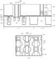
도 2f에 도시된 바와 같이, 셀 영역(ⅰ) 및 주변회로 영역(ⅱ)의 하드마스크층(120) 상부에 게이트를 정의하는 감광막 패턴(미도시)을 형성한 후, 감광막 패턴(미도시)을 마스크로 셀 영역(ⅰ)의 하드마스크층(120)을 식각하여 더미 게이트(미도시)를 형성하는 것이 바람직하다. 이 과정에서 반도체 기판(100) 하드마스크 패턴(106) 상부에 형성된 실링 절연막(110)은 식각되어 매립형 게이트(108) 상부에만 남는 것이 바람직하다. 이와 동시에, 감광막 패턴(미도시)을 마스크로 주변회로 영역(ⅱ)의 하드마스크층(120), 게이트 전극층(118), 배리어 도전층(116) 및 폴리실리콘층(114)을 식각하여 폴리실리콘 패턴(114a), 배리어 금속패턴(116), 게이트 전극 패턴(118a) 및 하드마스크 패턴(120a)으로 적층되는 동작 게이트(122R)를 형성하는 것이 바람직하다.As shown in FIG. 2F, after a photoresist pattern (not shown) defining a gate is formed on the
여기서 더미 게이트(미도시)는 도 2f의 (ⅲ)을 참조하여 설명한다. 도 2f의 (ⅲ)에 도시된 바와 같이 더미 게이트(122D)는 활성영역(104)의 중앙부를 노출시키는 섬타입인 것이 바람직하다. 이와 같이, 섬타입으로 더미 게이트(122D)를 형성하는 것은 후속 공정에서 형성되어 활성영역(104)의 중앙부와 연결되는 비트라인 콘택플러그 영역을 확보하기 위함이다. 또한, 더미 게이트(122D)는 후속 공정에서 저장전극 콘택홀 형성 시 장벽의 역할을 하여 자기정렬(self align)방식으로 용이하게 형성되도록 하는 역할을 한다. 보다 구체적인 설명은 도 2k에서 후술한다.Here, the dummy gate (not shown) will be described with reference to FIG. 2F. As shown in FIG. 2F, the
도 2g에 도시된 바와 같이, 셀 영역(ⅰ)의 더미 게이트(122D)를 포함하는 하드마스크 패턴(106) 및 실링 절연막(110)과 주변회로 영역(ⅱ)의 동작 게이트(122R)를 포함하는 게이트 산화막(112) 상부에 스페이서 절연막(124)을 형성한다. 여기서 스페이서 절연막(124)은 질화막을 포함하는 것이 바람직하다.As shown in FIG. 2G, the
도 2h에 도시된 바와 같이, 스페이서 절연막(124)이 형성된 셀 영역(ⅰ)의 더미 게이트(122D) 및 주변회로 영역(ⅱ)의 동작 게이트(122R) 상부에 층간절연막(126)을 형성한 후, 하드마스크 패턴(120a)이 노출되도록 평탄화 식각 공정을 수행하는 것이 바람직하다. 이때 층간절연막(126)은 BPSG(Boron Phorous Silcate Glass)를 포함하는 것이 바람직하며, 층간절연막(126) 형성 후 어닐링 공정을 수행하는 것이 바람직하다.As shown in FIG. 2H, after the interlayer insulating
도 2i에 도시된 바와 같이, 층간절연막(126) 상부에 비트라인 콘택홀을 정의하는 감광막 패턴(미도시)을 형성한 후, 이를 마스크로 더미 활성영역(104)이 노출되도록 층간절연막(126)을 식각하여 비트라인 콘택홀(128)을 형성한다. 여기서, 비트라인 콘택홀(128)은 더미 게이트(122D)와 상이한 식각선택비를 이용하여 층간절연막(126)을 식각함으로써 형성되는 것이 바람직하다. 즉, 도 2i의 (ⅲ)에 도시된 바와 같이, 비트라인 콘택홀(128)은 활성영역(104)의 중앙부가 노출되도록 형성되는 것이 바람직하며, 더미 게이트(122D)와의 식각선택비를 이용하여 형성되기 때문에 더미 게이트(122D)의 손실은 방지되고 그 사이 영역에 형성되는 것이 바람직하다.As shown in FIG. 2I, after forming a photoresist pattern (not shown) defining a bit line contact hole on the
도 2j에 도시된 바와 같이, 비트라인 콘택홀(128) 상부에 스페이서 절연막을 형성한 후 에치백을 수행하여 비트라인 콘택홀(128) 측벽에 스페이서(130)를 형성하는 것이 바람직하다. 이어서, 비트라인 콘택홀(128)이 매립되도록 도전층을 형성한 후, 층간절연막(126)이 노출되도록 도전층에 평탄화 식각 공정을 수행하여 비트라인 콘택플러그(132)를 형성한다. 비트라인 콘택플러그(132)는 도 2j의 (ⅲ)에 도시된 바와 같이, 활성영역(104)과 연결되며 더미 게이트(122D) 사이에 매립되는 것이 바람직하다.As illustrated in FIG. 2J, the spacer insulation layer may be formed on the sidewalls of the bit
도 2k에 도시된 바와 같이, 층간절연막(126) 상부에 저장전극 콘택홀을 정의하는 감광막 패턴(미도시)을 형성한 후 이를 마스크로 활성영역(104)이 노출되도록 층간절연막(126)을 식각하여 저장전극 콘택홀(134)을 형성한다. 여기서 저장전극 콘택홀(134)은 더미 게이트(122D)를 이용한 자기정렬(Self align) 방식으로 형성되는 것이 바람직하다. 즉, 저장전극 콘택홀(134)은 감광막 패턴(미도시)을 식각마스크로 더미 게이트(122D)와의 자기정렬방식으로 층간절연막(126)을 식각함으로써 형성되므로 저장전극 콘택홀(134)이 오정렬되는 것을 근본적으로 방지할 수 있다. 더욱이 더미 게이트(122D)는 전극층을 포함하지 않고 절연막으로만 형성되기 때문에 저장전극 콘택플러그와 비트라인 콘택플러그가 쇼트되는 불량이 근본적으로 발생하지 않는다.As shown in FIG. 2K, after forming a photoresist pattern (not shown) defining a storage electrode contact hole on the
이어서, 저장전극 콘택홀(134)이 매립되도록 도전층을 형성한 후, 층간절연막(126)이 노출되도록 도전층에 평탄화 식각 공정을 수행하여 저장전극 콘택플러그(136)를 형성하는 것이 바람직하다. 저장전극 콘택플러그(136)는 도 2k의 (ⅲ)에 도시된 바와 같이 더미 게이트(122D)에 의해 비트라인 콘택플러그(132)와 쇼트되는 것을 용이하게 방지할 수 있다.Subsequently, after the conductive layer is formed to fill the storage
도 2l에 도시된 바와 같이, 비트라인 콘택플러그(132, 도 2k 참조)를 포함하는 층간절연막(126) 상부에 비트라인 전극층 및 하드마스크층(미도시)을 형성한 후, 하드마스크층(미도시) 상에 비트라인 콘택플러그(132, 도 2k 참조)의 상부 연장선상에 있고 더미 게이트(122D)와 평행하는 감광막 패턴(미도시)을 형성한다. 그리고, 이를 마스크로 비트라인 전극층을 식각하여 비트라인(138)을 형성하는 것이 바람직하다. 비트라인(138)은 도 2l의 (ⅲ)에 도시된 바와 같이, 비트라인 콘택플러그(132, 도 2k 참조)와 연결되며 더미 게이트(122D)와 평행하도록 형성되는 것이 바람직하다.As shown in FIG. 2L, a bit line electrode layer and a hard mask layer (not shown) are formed on the
상술한 바와 같이, 본 발명은 저장전극 콘택플러그 형성 시 셀 영역에 형성된 더미 게이트와의 자기정렬식각 방법으로 형성되므로 오정렬을 근본적으로 방지하며 더미 게이트는 전극층을 포함하고 있지 않아 저장전극 콘택플러그와 쇼트되는 문제를 근본적으로 방지할 수 있다.As described above, the present invention is formed by a self-aligned etching method with the dummy gate formed in the cell region when the storage electrode contact plug is formed, thereby fundamentally preventing misalignment. Since the dummy gate does not include the electrode layer, the storage electrode contact plug and the short are not included. Can be fundamentally prevented.
본 발명은 기재된 실시예에 한정하는 것이 아니고, 본 발명의 사상 및 범위를 벗어나지 않는 한 다양하게 수정 및 변형을 할 수 있음은 당업자에게 자명하다고 할 수 있는 바, 그러한 변형예 또는 수정예들은 본 발명의 특허청구범위에 속하는 것이다.It will be apparent to those skilled in the art that various modifications and variations can be made in the present invention without departing from the spirit and scope of the invention as defined by the appended claims. Of the present invention.
Claims (22)
Translated fromKorean상기 활성영역의 상부에 구비되며 상기 활성영역의 중앙부 및 양단부를 노출시키는 더미 게이트;
상기 더미 게이트 사이에 구비되며 상기 활성영역의 중앙부와 연결되는 비트라인 콘택플러그; 및
상기 더미 게이트에 의해 상기 비트라인 콘택플러그와 이격되며 상기 활성영역의 양단부와 연결되는 저장전극 콘택플러그를 포함하는 것을 특징으로 하는 반도체 소자.A semiconductor substrate including a cell region and a peripheral circuit region and including an active region defined as an isolation layer;
A dummy gate disposed above the active region and exposing a central portion and both ends of the active region;
A bit line contact plug provided between the dummy gates and connected to a central portion of the active region; And
And a storage electrode contact plug spaced apart from the bit line contact plug by the dummy gate and connected to both ends of the active region.
상기 더미 게이트는
절연막을 포함하는 것을 특징으로 하는 반도체 소자.The method according to claim 1,
The dummy gate is
A semiconductor device comprising an insulating film.
상기 셀 영역 내에 매립된 매립형 게이트를 더 포함하는 것을 특징으로 하는 반도체 소자.The method according to claim 1,
And a buried gate embedded in the cell region.
상기 비트라인 콘택플러그를 둘러싸는 스페이서를 더 포함하는 것을 특징으로 하는 반도체 소자.The method according to claim 1,
And a spacer surrounding the bit line contact plug.
상기 비트라인 콘택플러그 상부와 연결되며, 상기 더미 게이트와 평행하는 비트라인을 더 포함하는 것을 특징으로 하는 반도체 소자.The method according to claim 1,
And a bit line connected to an upper portion of the bit line contact plug and parallel to the dummy gate.
상기 비트라인 콘택플러그, 상기 저장전극 콘택플러그 및 상기 더미 게이트의 사이를 매립하는 층간절연막을 더 포함하는 것을 특징으로 하는 반도체 소자.The method according to claim 1,
And an interlayer insulating layer filling the bit line contact plug, the storage electrode contact plug, and the dummy gate.
상기 주변회로 영역의 상기 반도체 기판 상부에 구비된 동작 게이트를 더 포함하는 것을 특징으로 하는 반도체 소자.The method according to claim 1,
And an operation gate provided on the semiconductor substrate in the peripheral circuit region.
상기 더미 게이트는 상기 동작 게이트와 동일한 높이를 갖는 것을 특징으로 하는 반도체 소자.The method according to claim 7,
And the dummy gate has the same height as the operation gate.
상기 더미 게이트 사이에 상기 활성영역의 중앙부와 연결되는 비트라인 콘택플러그를 형성하는 단계; 및
상기 더미 게이트에 의해 상기 비트라인 콘택플러그와 이격되며 상기 활성영역의 양단부와 연결되는 저장전극 콘택플러그를 형성하는 단계를 포함하는 것을 특징으로 하는 반도체 소자의 형성 방법.Forming a dummy gate on the semiconductor substrate including a cell region and a peripheral circuit region and exposing a center portion and both ends of the active region on an upper portion of the semiconductor substrate including an active region defined as an isolation layer;
Forming a bit line contact plug between the dummy gate and the center portion of the active region; And
Forming a storage electrode contact plug spaced apart from the bit line contact plug by the dummy gate and connected to both ends of the active region.
상기 더미 게이트를 형성하는 단계 이전
상기 셀 영역의 상기 반도체 기판 내에 매립되는 매립형 게이트를 형성하는 단계를 더 포함하는 것을 특징으로 하는 반도체 소자의 형성 방법.The method according to claim 9,
Before forming the dummy gate
Forming a buried gate embedded in the semiconductor substrate in the cell region.
상기 매립형 게이트를 형성하는 단계 이후
상기 주변회로 영역에 게이트 산화막을 형성하는 단계;
상기 게이트 산화막 상부에 폴리실리콘층을 형성하는 단계;
상기 폴리실리콘층 상부에 배리어 도전층을 형성하는 단계; 및
상기 배리어 도전층 상부에 게이트 금속층을 형성하는 단계를 더 포함하는 것을 특징으로 하는 반도체 소자의 형성 방법.The method according to claim 10,
After forming the buried gate
Forming a gate oxide film in the peripheral circuit region;
Forming a polysilicon layer on the gate oxide layer;
Forming a barrier conductive layer on the polysilicon layer; And
And forming a gate metal layer on the barrier conductive layer.
상기 배리어 도전층을 형성하는 단계 이후
상기 셀 영역의 상기 반도체 기판 및 상기 주변회로 영역의 상기 게이트 금속층 상부에 하드마스크층을 형성하는 단계를 더 포함하는 것을 특징으로 하는 반도체 소자의 형성 방법.The method of claim 11,
After forming the barrier conductive layer
And forming a hard mask layer over the semiconductor substrate in the cell region and the gate metal layer in the peripheral circuit region.
상기 더미 게이트를 형성하는 단계는
상기 하드마스크층 상부에 마스크 패턴을 형성하는 단계;
상기 마스크 패턴을 식각마스크로 상기 활성영역의 중앙부 및 상기 활성영역의 양단부가 노출되도록 상기 셀 영역의 하드마스크층을 식각하는 단계를 포함하는 것을 특징으로 하는 반도체 소자의 형성 방법.The method of claim 12,
Forming the dummy gate
Forming a mask pattern on the hard mask layer;
Etching the hard mask layer of the cell region to expose the center portion of the active region and both ends of the active region with the mask pattern as an etch mask.
상기 더미 게이트를 형성하는 단계와 동시에
상기 마스크 패턴을 식각마스크로 상기 주변회로 영역의 상기 하드마스크층, 상기 폴리실리콘층, 상기 배리어 도전층 및 상기 게이트 금속층을 식각하여 동작 게이트를 형성하는 것을 특징으로 하는 반도체 소자의 형성 방법.The method according to claim 13,
Simultaneously with forming the dummy gate
And forming an operation gate by etching the hard mask layer, the polysilicon layer, the barrier conductive layer, and the gate metal layer in the peripheral circuit area using the mask pattern as an etch mask.
상기 동작 게이트를 형성하는 단계 이후
상기 셀 영역의 반도체 기판 및 상기 주변회로 영역의 동작 게이트 측벽에 스페이서 절연막을 형성하는 단계를 더 포함하는 것을 특징으로 하는 반도체 소자의 형성 방법.The method according to claim 14,
After forming the operation gate
And forming a spacer insulating film on sidewalls of the semiconductor substrate in the cell region and the operation gate of the peripheral circuit region.
상기 동작 게이트를 형성하는 단계 이후
상기 더미 게이트 및 상기 동작 게이트 사이가 매립되도록 상기 셀 영역 및 상기 주변회로 영역에 층간절연막을 형성하는 단계를 더 포함하는 것을 특징으로 하는 반도체 소자의 형성 방법.The method according to claim 15,
After forming the operation gate
And forming an interlayer insulating film in the cell region and the peripheral circuit region so as to fill the gap between the dummy gate and the operation gate.
상기 비트라인 콘택플러그를 형성하는 단계는
상기 층간절연막 상부에 비트라인 콘택홀을 정의하는 마스크 패턴을 형성하는 단계;
상기 마스크 패턴을 식각마스크로 상기 활성영역의 중앙부가 노출되도록 상기 층간절연막을 식각하여 비트라인 콘택홀을 형성하는 단계; 및
상기 비트라인 콘택홀이 매립되도록 도전층을 형성하는 단계를 포함하는 것을 특징으로 하는 반도체 소자의 형성 방법.The method according to claim 16,
Forming the bit line contact plug
Forming a mask pattern defining a bit line contact hole on the interlayer insulating layer;
Forming a bit line contact hole by etching the interlayer insulating layer so that the center portion of the active region is exposed using the mask pattern as an etch mask; And
And forming a conductive layer to fill the bit line contact holes.
상기 비트라인 콘택홀을 형성하는 단계는
상기 더미 게이트와의 식각선택비를 이용하여 상기 층간절연막을 식각하는 것을 특징으로 하는 반도체 소자의 형성 방법.18. The method of claim 17,
Forming the bit line contact hole
And etching the interlayer dielectric layer using an etch selectivity with the dummy gate.
상기 비트라인 콘택플러그를 형성하는 단계 이전
상기 비트라인 콘택홀 내부에 스페이서를 형성하는 단계를 더 포함하는 것을 특징으로 하는 반도체 소자의 형성 방법.18. The method of claim 17,
Before forming the bit line contact plug
And forming a spacer in the bit line contact hole.
상기 저장전극 콘택플러그를 형성하는 단계는
상기 층간절연막 상부에 저장전극 콘택홀을 정의하는 마스크 패턴을 형성하는 단계;
상기 마스크 패턴을 식각마스크로 상기 활성영역의 양단부가 노출되도록 상기 층간절연막을 식각하여 저장전극 콘택홀을 형성하는 단계; 및
상기 저장전극 콘택홀이 매립되도록 도전층을 형성하는 단계를 포함하는 것을 특징으로 하는 반도체 소자의 형성 방법.The method according to claim 16,
Forming the storage electrode contact plug
Forming a mask pattern defining a storage electrode contact hole on the interlayer insulating layer;
Etching the interlayer insulating layer to expose both ends of the active region using the mask pattern as an etch mask to form a storage electrode contact hole; And
And forming a conductive layer to fill the storage electrode contact hole.
상기 저장전극 콘택홀을 형성하는 단계는
상기 더미 게이트와의 자기정렬방식으로 수행되는 것을 특징으로 하는 반도체 소자의 형성 방법.The method of claim 20,
Forming the storage electrode contact hole
And forming the semiconductor device in a self-aligned manner with the dummy gate.
상기 저장전극 콘택플러그를 형성하는 단계 이후,
상기 비트라인 콘택플러그 상부와 연결되며 상기 더미 게이트와 평행하는 비트라인을 형성하는 단계를 더 포함하는 것을 특징으로 하는 반도체 소자의 형성 방법.The method according to claim 9,
After forming the storage electrode contact plug,
And forming a bit line connected to an upper portion of the bit line contact plug and parallel to the dummy gate.
Priority Applications (2)
| Application Number | Priority Date | Filing Date | Title |
|---|---|---|---|
| KR1020100130008AKR101095739B1 (en) | 2010-12-17 | 2010-12-17 | Semiconductor element and method of forming the same |
| US13/182,175US8492812B2 (en) | 2010-12-17 | 2011-07-13 | Semiconductor device having dummy pattern and method of fabricating a semiconductor device comprising dummy pattern |
Applications Claiming Priority (1)
| Application Number | Priority Date | Filing Date | Title |
|---|---|---|---|
| KR1020100130008AKR101095739B1 (en) | 2010-12-17 | 2010-12-17 | Semiconductor element and method of forming the same |
Publications (1)
| Publication Number | Publication Date |
|---|---|
| KR101095739B1true KR101095739B1 (en) | 2011-12-21 |
Family
ID=45506538
Family Applications (1)
| Application Number | Title | Priority Date | Filing Date |
|---|---|---|---|
| KR1020100130008AExpired - Fee RelatedKR101095739B1 (en) | 2010-12-17 | 2010-12-17 | Semiconductor element and method of forming the same |
Country Status (2)
| Country | Link |
|---|---|
| US (1) | US8492812B2 (en) |
| KR (1) | KR101095739B1 (en) |
Cited By (1)
| Publication number | Priority date | Publication date | Assignee | Title |
|---|---|---|---|---|
| US9196620B2 (en) | 2012-11-26 | 2015-11-24 | Samsung Electronics Co., Ltd. | Semiconductor devices and methods of manufacturing the same |
Families Citing this family (4)
| Publication number | Priority date | Publication date | Assignee | Title |
|---|---|---|---|---|
| US8716077B2 (en)* | 2011-08-23 | 2014-05-06 | Globalfoundries Inc. | Replacement gate compatible eDRAM transistor with recessed channel |
| KR102280238B1 (en) | 2015-01-30 | 2021-07-20 | 삼성전자주식회사 | Method for fabricating semiconductor device |
| CN108461449B (en)* | 2017-02-20 | 2019-09-17 | 联华电子股份有限公司 | Semiconductor element and manufacturing method thereof |
| CN108538839B (en)* | 2017-03-01 | 2019-08-23 | 联华电子股份有限公司 | Semiconductor structure, semiconductor structure for memory element and manufacturing method thereof |
Citations (2)
| Publication number | Priority date | Publication date | Assignee | Title |
|---|---|---|---|---|
| KR100620655B1 (en) | 2004-12-30 | 2006-09-13 | 주식회사 하이닉스반도체 | Recess gate formation method of semiconductor device |
| JP2010141107A (en) | 2008-12-11 | 2010-06-24 | Elpida Memory Inc | Semiconductor device and method of manufacturing the same |
Family Cites Families (3)
| Publication number | Priority date | Publication date | Assignee | Title |
|---|---|---|---|---|
| KR100375428B1 (en)* | 1995-11-20 | 2003-05-17 | 가부시끼가이샤 히다치 세이사꾸쇼 | Semiconductor storage device and process for manufacturing the same |
| KR20030002701A (en) | 2001-06-29 | 2003-01-09 | 주식회사 하이닉스반도체 | Method of manufacturing a transistor in a semiconductor device |
| KR20090098291A (en) | 2008-03-13 | 2009-09-17 | 주식회사 하이닉스반도체 | Semiconductor device and method for manufacturing the same |
- 2010
- 2010-12-17KRKR1020100130008Apatent/KR101095739B1/ennot_activeExpired - Fee Related
- 2011
- 2011-07-13USUS13/182,175patent/US8492812B2/ennot_activeExpired - Fee Related
Patent Citations (2)
| Publication number | Priority date | Publication date | Assignee | Title |
|---|---|---|---|---|
| KR100620655B1 (en) | 2004-12-30 | 2006-09-13 | 주식회사 하이닉스반도체 | Recess gate formation method of semiconductor device |
| JP2010141107A (en) | 2008-12-11 | 2010-06-24 | Elpida Memory Inc | Semiconductor device and method of manufacturing the same |
Cited By (1)
| Publication number | Priority date | Publication date | Assignee | Title |
|---|---|---|---|---|
| US9196620B2 (en) | 2012-11-26 | 2015-11-24 | Samsung Electronics Co., Ltd. | Semiconductor devices and methods of manufacturing the same |
Also Published As
| Publication number | Publication date |
|---|---|
| US20120153369A1 (en) | 2012-06-21 |
| US8492812B2 (en) | 2013-07-23 |
Similar Documents
| Publication | Publication Date | Title |
|---|---|---|
| US11563012B2 (en) | Semiconductor structure with capacitor landing pad and method of making the same | |
| KR101051577B1 (en) | Semiconductor element and formation method thereof | |
| KR101205173B1 (en) | Method for forming semiconductor device | |
| US7696570B2 (en) | Transistors of semiconductor device having channel region in a channel-portion hole and methods of forming the same | |
| KR100689712B1 (en) | Method for manufacturing semiconductor memory device and its structure | |
| KR101910129B1 (en) | Semiconductor device and method for using the same | |
| KR20110063204A (en) | Semiconductor element and formation method thereof | |
| JP2005079576A (en) | Semiconductor device and manufacturing method thereof | |
| US11367727B2 (en) | Memory structure | |
| KR101095739B1 (en) | Semiconductor element and method of forming the same | |
| KR101095787B1 (en) | Semiconductor device and method of forming the same | |
| CN110534150B (en) | Memory device and method of manufacturing the same | |
| KR100939110B1 (en) | Semiconductor device and manufacturing method thereof | |
| KR101177486B1 (en) | Semiconductor device and method for forming the same | |
| KR20120067128A (en) | Method for manufacturing semiconductor device | |
| KR101120185B1 (en) | Method for forming semiconductor device | |
| US20240032286A1 (en) | Integrated circuit devices | |
| KR20120087586A (en) | Semiconductor device and method for forming the same | |
| KR20120120793A (en) | Semiconductor device and method for forming the same | |
| KR20110091211A (en) | Method of manufacturing semiconductor device | |
| KR20120034990A (en) | Semiconductor device and method for forming the same | |
| KR20070069755A (en) | Manufacturing method of semiconductor device | |
| KR20120027697A (en) | Semiconductor device and method for forming the same | |
| KR20120029885A (en) | Semiconductor device and method for forming the same | |
| KR20080029256A (en) | Capacitor Formation Method of Semiconductor Device |
Legal Events
| Date | Code | Title | Description |
|---|---|---|---|
| A201 | Request for examination | ||
| PA0109 | Patent application | St.27 status event code:A-0-1-A10-A12-nap-PA0109 | |
| PA0201 | Request for examination | St.27 status event code:A-1-2-D10-D11-exm-PA0201 | |
| D13-X000 | Search requested | St.27 status event code:A-1-2-D10-D13-srh-X000 | |
| D14-X000 | Search report completed | St.27 status event code:A-1-2-D10-D14-srh-X000 | |
| E701 | Decision to grant or registration of patent right | ||
| PE0701 | Decision of registration | St.27 status event code:A-1-2-D10-D22-exm-PE0701 | |
| GRNT | Written decision to grant | ||
| PR0701 | Registration of establishment | St.27 status event code:A-2-4-F10-F11-exm-PR0701 | |
| PR1002 | Payment of registration fee | St.27 status event code:A-2-2-U10-U11-oth-PR1002 Fee payment year number:1 | |
| PG1601 | Publication of registration | St.27 status event code:A-4-4-Q10-Q13-nap-PG1601 | |
| PN2301 | Change of applicant | St.27 status event code:A-5-5-R10-R13-asn-PN2301 St.27 status event code:A-5-5-R10-R11-asn-PN2301 | |
| PN2301 | Change of applicant | St.27 status event code:A-5-5-R10-R13-asn-PN2301 St.27 status event code:A-5-5-R10-R11-asn-PN2301 | |
| FPAY | Annual fee payment | Payment date:20141126 Year of fee payment:4 | |
| PR1001 | Payment of annual fee | St.27 status event code:A-4-4-U10-U11-oth-PR1001 Fee payment year number:4 | |
| PN2301 | Change of applicant | St.27 status event code:A-5-5-R10-R13-asn-PN2301 St.27 status event code:A-5-5-R10-R11-asn-PN2301 | |
| FPAY | Annual fee payment | Payment date:20151120 Year of fee payment:5 | |
| PR1001 | Payment of annual fee | St.27 status event code:A-4-4-U10-U11-oth-PR1001 Fee payment year number:5 | |
| LAPS | Lapse due to unpaid annual fee | ||
| PC1903 | Unpaid annual fee | St.27 status event code:A-4-4-U10-U13-oth-PC1903 Not in force date:20161213 Payment event data comment text:Termination Category : DEFAULT_OF_REGISTRATION_FEE | |
| PC1903 | Unpaid annual fee | St.27 status event code:N-4-6-H10-H13-oth-PC1903 Ip right cessation event data comment text:Termination Category : DEFAULT_OF_REGISTRATION_FEE Not in force date:20161213 | |
| P22-X000 | Classification modified | St.27 status event code:A-4-4-P10-P22-nap-X000 | |
| P22-X000 | Classification modified | St.27 status event code:A-4-4-P10-P22-nap-X000 |