KR101093785B1 - Semiconductors on SOI Substrates and Devices Formed therefrom - Google Patents
Semiconductors on SOI Substrates and Devices Formed therefromDownload PDFInfo
- Publication number
- KR101093785B1 KR101093785B1KR1020067023279AKR20067023279AKR101093785B1KR 101093785 B1KR101093785 B1KR 101093785B1KR 1020067023279 AKR1020067023279 AKR 1020067023279AKR 20067023279 AKR20067023279 AKR 20067023279AKR 101093785 B1KR101093785 B1KR 101093785B1
- Authority
- KR
- South Korea
- Prior art keywords
- layer
- scandate
- silicon
- semiconductor material
- lattice
- Prior art date
- Legal status (The legal status is an assumption and is not a legal conclusion. Google has not performed a legal analysis and makes no representation as to the accuracy of the status listed.)
- Expired - Fee Related
Links
Images


Classifications
- H—ELECTRICITY
- H01—ELECTRIC ELEMENTS
- H01L—SEMICONDUCTOR DEVICES NOT COVERED BY CLASS H10
- H01L21/00—Processes or apparatus adapted for the manufacture or treatment of semiconductor or solid state devices or of parts thereof
- H01L21/70—Manufacture or treatment of devices consisting of a plurality of solid state components formed in or on a common substrate or of parts thereof; Manufacture of integrated circuit devices or of parts thereof
- H01L21/71—Manufacture of specific parts of devices defined in group H01L21/70
- H01L21/76—Making of isolation regions between components
- H01L21/762—Dielectric regions, e.g. EPIC dielectric isolation, LOCOS; Trench refilling techniques, SOI technology, use of channel stoppers
- H01L21/7624—Dielectric regions, e.g. EPIC dielectric isolation, LOCOS; Trench refilling techniques, SOI technology, use of channel stoppers using semiconductor on insulator [SOI] technology
- H—ELECTRICITY
- H10—SEMICONDUCTOR DEVICES; ELECTRIC SOLID-STATE DEVICES NOT OTHERWISE PROVIDED FOR
- H10D—INORGANIC ELECTRIC SEMICONDUCTOR DEVICES
- H10D30/00—Field-effect transistors [FET]
- H10D30/60—Insulated-gate field-effect transistors [IGFET]
- H10D30/67—Thin-film transistors [TFT]
- H10D30/674—Thin-film transistors [TFT] characterised by the active materials
- H10D30/6741—Group IV materials, e.g. germanium or silicon carbide
- H—ELECTRICITY
- H10—SEMICONDUCTOR DEVICES; ELECTRIC SOLID-STATE DEVICES NOT OTHERWISE PROVIDED FOR
- H10D—INORGANIC ELECTRIC SEMICONDUCTOR DEVICES
- H10D30/00—Field-effect transistors [FET]
- H10D30/60—Insulated-gate field-effect transistors [IGFET]
- H10D30/67—Thin-film transistors [TFT]
- H10D30/6758—Thin-film transistors [TFT] characterised by the insulating substrates
- H—ELECTRICITY
- H10—SEMICONDUCTOR DEVICES; ELECTRIC SOLID-STATE DEVICES NOT OTHERWISE PROVIDED FOR
- H10D—INORGANIC ELECTRIC SEMICONDUCTOR DEVICES
- H10D30/00—Field-effect transistors [FET]
- H10D30/60—Insulated-gate field-effect transistors [IGFET]
- H10D30/791—Arrangements for exerting mechanical stress on the crystal lattice of the channel regions
Landscapes
- Engineering & Computer Science (AREA)
- Microelectronics & Electronic Packaging (AREA)
- Condensed Matter Physics & Semiconductors (AREA)
- General Physics & Mathematics (AREA)
- Manufacturing & Machinery (AREA)
- Computer Hardware Design (AREA)
- Physics & Mathematics (AREA)
- Power Engineering (AREA)
- Thin Film Transistor (AREA)
- Insulated Gate Type Field-Effect Transistor (AREA)
- Inorganic Insulating Materials (AREA)
- Crystals, And After-Treatments Of Crystals (AREA)
- Recrystallisation Techniques (AREA)
- Metal-Oxide And Bipolar Metal-Oxide Semiconductor Integrated Circuits (AREA)
Abstract
Translated fromKorean
Description
Translated fromKorean본 발명은 일반적으로 절연 게이트 전계효과 트랜지스터(MOSFET)의 제조에 관한 것으로, 특히 절연 기판 위에 형성된 MOSFET에 관한 것이다.BACKGROUND OF THE INVENTION Field of the Invention The present invention generally relates to the manufacture of insulated gate field effect transistors (MOSFETs), and more particularly to MOSFETs formed over insulating substrates.
MOSFET 는 집적회로(IC)의 일반적인 구성소자이다. 도 1은 통상적인 MOSFET 소자의 횡단면도이다. 상기 MOSFET는 얕은 트렌치 절연부(shallow trench isolation : 12)에 의해 경계가 지워진 활성 영역내의 벌크 실리콘 기판(10)위에 제조된다. 얕은 트렌치 절연부(12)는 상기 기판(10) 위에 제조된 다른 IC 구성소자로부터 상기 MOSFET의 활성 영역을 전기적으로 절연한다. 상기 MOSFET는 실리콘 옥사이드(silicon oxide) 또는 실리콘 옥시나이트라이드(silicon oxynitride)와 같은 게이트 절연체(18)에 의해 분리되는 게이트(14)와 채널 영역(16)으로 이루어진다. 상기 게이트(14)는 일반적으로 폴리실리콘(polysilicon)과 같이 밀도 높게 도핑된 반도체 물질로 형성된다. 상기 MOSFET의 소오스와 드레인 영역은 상기 채널 영역(16)을 마주보고 형성된 얕은 소오스 및 드레인 영역(24)과 깊은 소오스 및 드레인 영역(20)으로 이루어진다. 상기 얕은 소오스 및 드레인 영역(24)은 상기 기판위에 보호층(26)을 형성한 다음 주입된다. 그 다음 상기 깊은 소오스 및 드레인 영역(20)은 게이트(14) 주위에 스페이서(22)를 형성한 다음 이온 주입법으로 형성된다. 소오스와 드레인 실리사이드(silicide; 28)는, 옴 접촉(ohmic contacts)를 제공하고 접촉 저항을 감소시키기 위하여 상기 깊은 소오스 및 드레인 영역(20)에 형성된다. 실리사이드(28)는 코발트(Co) 또는 니켈(Ni)과 같은 금속 및 기판 반도체 물질로 구성된다. 실리사이드(30)가 또한 상기 게이트(14)의 상부 표면에 형성된다.MOSFETs are a common component of integrated circuits (ICs). 1 is a cross-sectional view of a typical MOSFET device. The MOSFET is fabricated on a
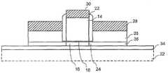
벌크 반도체 기판위에 소자를 형성하는 다른 방법이 SOI(semiconductor on insulator) 구조이다. SOI 구조에 있어서, MOSFET 는 상기 MOSFET 활성 영역 아래에 유전체 물질층을 포함하는 기판 위에 형성된다. SOI 소자는 벌크 반도체 기판상에 제조되는 것보다 많은 장점을 가진다. 예를 들면, 소자간 더 나은 절연성, 누설전류의 감소, CMOS 소자 사이에 래치-업(latch-up) 감소, 칩 캐패시턴스(chip capacitance) 감소 및 소오스와 드레인 영역 사이에 쇼트 채널 커플링(short channel coupling)의 감소 또는 제거 등이다. 도 2는 통상적인 완전 공핍된(fully depleted) SOI MOSFET 의 일 예를 도시한 도면이다. 상기 SOI MOSFET 는 실리콘층(32)과 유전체층(34)으로 구성된 SOI 기판에 형성된다. 상기 MOSFET 구조는 개별적인 소자가 형성되어 있는 개별적인 아일랜드(island)를 한정하기 위하여 식각된 실리콘층의 절연 영역(36)에 형성된다. 얇은 도핑 되지 않은 채널 영역(16)이 상기 실리콘 영역(36)의 중심에 있다. 소오스와 드레인 확장부(24)는 게이트 절연체(18) 위에 형성된 게이트(14)의 양 측면에서 실리콘 영역(36)으로 주입된다. 스페이서(22)의 형성에 후속하여, 상승한(elevated) 소오스와 드레인 영역(38)은 상기 실리콘 영역(38)에서 성장하고, 실리사이드 소오스, 드레인 콘택(contact; 28) 및 규실리사이드 게이트 콘택(30)이 그 다음으로 형성된다.Another method of forming devices on a bulk semiconductor substrate is a semiconductor on insulator (SOI) structure. In an SOI structure, a MOSFET is formed over a substrate including a layer of dielectric material below the MOSFET active region. SOI devices have many advantages over being manufactured on bulk semiconductor substrates. For example, better isolation between devices, reduced leakage current, reduced latch-up between CMOS devices, reduced chip capacitance, and short channel coupling between source and drain regions. reducing or eliminating coupling). 2 shows an example of a typical fully depleted SOI MOSFET. The SOI MOSFET is formed on an SOI substrate composed of a
MOSFET 성능을 향상시키기 위한 한 가지 선택은 저항 및 전력 소모를 줄이고 구동 전류, 주파수 응답 및 동작 속도를 증가시키기 위하여 반도체 물질의 캐리어 이동성을 증가시키는 것이다. 캐리어 이동성을 증가시키는 것으로 최근 관심을 집중시키는 방법은, 변형(strain)이 인가된 실리콘 물질을 사용하는 것이다. 신장 변형된 실리콘(tensile strained silicon)은 실리콘 게르마늄 기판 위에 반도체의 에피택셜층(epitaxial layer)을 성장시켜 형성될 수 있다. 상기 실리콘 게르마늄 격자(silicon germanium lattice)는 상기 격자 내에서 더욱 커진 게르마늄 원자의 존재때문에 순수 실리콘 격자보다 다소 커진 격자 상수를 가진다. 에피택셜 성장된 실리콘은 상기 실리콘 게르마늄 격자에 스스로 정렬한 후, 신장 변형이 상기 실리콘 격자에서 생성된다. 적당한 신장 변형(moderate tensile strain)은 전자의 이동성을 증가시키고, 더 많은 양의(more substantial) 신장 변형은 홀의 이동성을 증가시킨다. 신장 변형의 양은 상기 실리콘 게르마늄 격자에 있는 게르마늄 비율에 따라 증가한다. 적당한 압축 변형 역시 홀의 이동성을 증가시킨다고 알려져 있다.One option to improve MOSFET performance is to increase the carrier mobility of the semiconductor material to reduce resistance and power consumption and to increase drive current, frequency response and operating speed. A recent focus of attention to increasing carrier mobility is the use of silicone materials to which strain has been applied. Stretched strained silicon may be formed by growing an epitaxial layer of a semiconductor on a silicon germanium substrate. The silicon germanium lattice has a lattice constant somewhat larger than pure silicon lattice due to the presence of larger germanium atoms in the lattice. After the epitaxially grown silicon aligns itself with the silicon germanium lattice, stretch strain is created in the silicon lattice. Moderate tensile strain increases the mobility of the electrons, and more substantial stretch strain increases the mobility of the holes. The amount of stretch strain increases with the germanium ratio in the silicon germanium lattice. Proper compressive deformation is also known to increase hole mobility.
신장 변형된 실리콘층을 내장한 MOSFET 의 일 예가 도 3에 도시되어 있다. 상기 MOSFET 는 실리콘층(10)에서 성장한 실리콘 게르마늄층(32)을 포함한 기판 위에 제조된다. 상기 실리콘 게르마늄층은, 전형적으로 원하는 변형의 양에 따라, 게르마늄 내용물이 0 에서 10% 내지 40% 사이까지 점진적으로 증가되는, 경사진 층(graded layer)이다. 변형된 실리콘(34) 에피택셜층은 상기 실리콘 게르마늄층(32)에서 성장된다. 상기 MOSFET 는 깊은 소오스 및 드레인영역(20), 얕은 소오스 및 드레인 확장부(24), 게이트 산화물층(18), 보호층(16)으로 둘러싸인 게이트(14), 스페이서(22), 소오스 및 드레인 실리사이드(28), 게이트 실리사이드(30) 및 얕은 트렌치 절연부(12)를 포함한 종래의 MOSFET 구조를 사용한다. 상기 채널 영역(16)내에 변형된 실리콘 물질은 상기 소오스와 드레인 사이에 향상된 캐리어 이동성을 제공한다.An example of a MOSFET with a stretched strained silicon layer is shown in FIG. 3. The MOSFET is fabricated on a substrate including a
변형된 실리콘은 또한 SOI 기판 위에 형성된 MOSFET에 내장될 수 있다. 도 4는 변형된 실리콘 SOI MOSFET의 일 예를 도시한 도면이다. 이러한 장치에 있어서, MOSFET 는 유전체층(40)위에 있는 실리콘 게르마늄층으로 이루어진 SOI 기판상에 형성된다. 상기 실리콘 게르마늄층은 개별적인 MOSFET 가 형성된 절연 영역(42)을 한정하기 위하여 패터닝된다. 변형된 실리콘층(44)은 상기 실리콘 게르마늄층에서 성장된다. 그런 다음, 상기 MOSFET 는 도 3의 종래 변형된 실리콘 장치와 유사한 방식으로 형성된다.The modified silicon can also be embedded in a MOSFET formed over an SOI substrate. 4 is a diagram illustrating an example of a modified silicon SOI MOSFET. In such a device, a MOSFET is formed on an SOI substrate consisting of a layer of silicon germanium over
변형된 실리콘 채널을 내장하는 완전 공핍된 SOI(fully depleted SOI) 장치를 제조하는 것은 매우 어렵다. 쇼트 채널 효과를 제어하기 위하여, 완전하게 공핍된 SOI MOSFET 는 대략 채널 길의의 삼분의 일을 넘지않는 채널 영역의 두께를 가지는 것이 바람직하다. 그러나, 상기 변형된 채널 아래에 실리콘 게르마늄의 지지층을 제공할 필요가 있으며, 총 채널 두께는 채널길이에 제한받게 되거나 또는 변형된 실리콘의 두께가 현저한 이동성 향상을 제공하기에는 충분하지가 않다.It is very difficult to fabricate a fully depleted SOI device that incorporates a strained silicon channel. To control the short channel effect, a fully depleted SOI MOSFET preferably has a thickness of the channel region that is approximately no more than one third of the channel length. However, it is necessary to provide a support layer of silicon germanium under the strained channel, and the total channel thickness is limited to the channel length or the thickness of the strained silicon is not sufficient to provide significant mobility improvement.
다른 고려사항들은 일반적으로 SOI 장치의 소형화에 대한 걸림돌로 남아있다. 종래의 완전하게 공핍된 SOI 장치에 있어서, 일반적으로 원하는 두께의 반도체 물질이 남아있을 때까지 화학 기계 연마(chemical mechanical pollishing; CMP)를 수행하여 상기 기판 위에 아주 얇은 채널층을 제조하였다. 그러나, CMP 는 100Å 정도의 두께 변동을 가질 수 있는 불균일한 표면을 생성한다. 임계 치수(critical dimension)가 감소함에 따라, 위와 같은 두께 변동성은 용납하기 어려워졌다. 예를 들면, 45nm 장치의 경우, 대략 150Å의 채널 영역 두께를 원하게 된다. 연마된 층의 두께가 변동한다면, 이러한 차원에서 정확한 두께를 가지는 채널 영역을 신뢰성 있게 제조하기 어렵다.Other considerations generally remain an obstacle to the miniaturization of SOI devices. In conventional fully depleted SOI devices, chemical mechanical pollishing (CMP) was generally performed until a semiconductor material of the desired thickness remained to produce a very thin channel layer on the substrate. However, CMP produces non-uniform surfaces that can have thickness variations as high as 100 microns. As the critical dimension is reduced, such thickness variability has become difficult to tolerate. For example, for 45 nm devices, a channel area thickness of approximately 150 Hz is desired. If the thickness of the polished layer varies, it is difficult to reliably manufacture channel regions with the correct thickness in this dimension.
완전히 균일한 두께의 채널 영역을 획득하기 위해서는, 유전체 물질 상에 반도체 물질층을 성장시키는 것이 바람직하다. 하지만, 종래의 반도체 장치 제조 기술에서는, 결정 격자의 사용은 추가적인 결정 물질의 성장을 위한 형판(template)으로서의 사용에 의존하고 있다. 예를 들면, 실리콘 웨이퍼는 규칙적인 결정 격자를 제공하기 위하여 결정 표면 중 한 면을 따라 절단된 단일 결정 실리콘으로 구성되었다. 이러한 격자는 증착(deposited)에 따라 정렬될 동일한 격자 구조를 가지는 실리콘 또는 다른 소자의 원자를 증착시키는 형판으로서 적당하고, 따라서, 부가적인 단결정 물질을 형성한다. 위와 같은 형판이 없으면, 증착된 실리콘은, 둘러싸인 그레인(grain)에 대하여 무작위로 편향된 결정 격자를 갖는 개별적인 그레인들 각각으로 구성된 다결정 실리콘 또는 비정질 실리콘의 형태를 취한다. 이러한 형태의 실리콘은 단결정 실리콘과 비교하여 불량한 전도성을 나타내기 때문에 MOSFET의 활성 영역에서 사용하기에 바람직하지 못하다. 따라서, 다른 물질, 특히 실리콘 옥사이드 및 실리콘 옥시나이트라이드와 같은 종래 유전체 위에서 단결정 실리콘을 성장시키는 것은 일반적으로 가능하지 않다. 그 구조는 본질적으로 비결정질이거나 상기 실리콘 격자와 부합하지 않는다.In order to obtain a channel region of completely uniform thickness, it is desirable to grow a semiconductor material layer on the dielectric material. However, in conventional semiconductor device fabrication techniques, the use of crystal lattice relies on its use as a template for the growth of additional crystalline materials. For example, a silicon wafer was composed of single crystal silicon cut along one side of the crystal surface to provide a regular crystal lattice. Such a grating is suitable as a template for depositing atoms of silicon or other devices having the same lattice structure to be aligned upon deposition, thus forming additional single crystal material. Without such a template, the deposited silicon takes the form of polycrystalline silicon or amorphous silicon, each composed of individual grains with a crystal lattice randomly deflected with respect to the enclosed grain. This type of silicon is undesirable for use in the active region of a MOSFET because it exhibits poor conductivity compared to single crystal silicon. Thus, it is generally not possible to grow single crystal silicon over other materials, particularly conventional dielectrics such as silicon oxide and silicon oxynitride. The structure is essentially amorphous or inconsistent with the silicon lattice.
따라서, 절연체 장치 위에서 반도체를 제조하는 종래 기술은 적은 임계 치수를 가지는 장치 및 변형된 실리콘을 내장하는 장치를 제조하는데 만족스럽지 못하였다.Thus, the prior art of manufacturing semiconductors over insulator devices has not been satisfactory for fabricating devices with small critical dimensions and devices incorporating strained silicon.
본 발명의 실시예들은 반도체층이 직접 성장될 수 있는 유전체층으로 구성된 SOI 디바이스들을 제공한다. 상기 유전체층의 특성과 상기 반도체층의 특성은 상기 유전체층이 신장성 변형 또는 압축성 변형을 반도체 물질에 부여하도록 선택될 수 있다.Embodiments of the present invention provide SOI devices comprised of a dielectric layer in which a semiconductor layer can be grown directly. The properties of the dielectric layer and the properties of the semiconductor layer may be selected such that the dielectric layer imparts stretchable or compressive strain to the semiconductor material.
본 발명의 다른 실시예는 위와 같은 장치를 형성하는 방법을 제공한다.Another embodiment of the present invention provides a method of forming such a device.
본 발명의 특정한 바람직한 실시예는 페로브스카이트 격자 구조(perovskite lattice structure)를 가지는 유전체 물질층을 사용한다. 페로브스카이트 구조는 다이아몬드 격자 반도체의 성장에 필요한 적절한 형판을 제공하는 것으로 알려져 있다. 페로브스카이트 격자 구조를 가지는 유전체의 예들은 가돌리늄 스캔데이트(gadolinium scandate; GdScO3), 디스프로슘 스캔데이트(dysprosium scandate; DyScO3) 및 가돌리늄과 디스프로슘 스캔데이트의 합금(alloys of gadolinium and dysprosium scandate; Gd1-xDyxScO3)과 같은 희토 스캔데이트 화합물(rare earth scandate compounds)을 포함한다. 상기 희토 스캔데이트와 양립하는 다이아몬드 격자 구조를 가지는 반도체 물질은 일예는 실리콘, 게르마늄, 실리콘과 게르마늄의 합금 및 갈륨 아르세나이드(gallium arsenide)와 같은 III-V 형 반도체 물질을 포함한다. 희토 스캔데이트와 반도체 물질의 화학량론적 구조는 상기 희토 스캔데이트가 신장성 변형 또는 압축성 변형을 그 위에서 성장한 상기 반도체 물질에 부여하도록 설계될 수 있다. 위와 같은 유전체 물질은 상기 유전체층 위에 얇은 반도체층이 직접 성장하는 것을 허용하여, 절연체 MOSFET 상의 반도체에서 유전체층으로 사용될 수 있다.Certain preferred embodiments of the present invention employ a layer of dielectric material having a perovskite lattice structure. Perovskite structures are known to provide suitable templates for the growth of diamond lattice semiconductors. Examples of dielectrics with perovskite lattice structures include gadolinium scandate (GdScO3 ), dysprosium scandate (DyScO3 ), and alloys of gadolinium and dysprosium scandate (GdScO3 ). Rare earth scandate compounds such as1-x Dyx ScO3 ). Semiconductor materials having a diamond lattice structure compatible with the rare earth scandate include, for example, III-V type semiconductor materials such as silicon, germanium, an alloy of silicon and germanium, and gallium arsenide. The stoichiometric structure of the rare earth scandate and the semiconductor material may be designed such that the rare earth scandate imparts stretchable or compressive strain to the semiconductor material grown thereon. The above dielectric material allows a thin semiconductor layer to grow directly on the dielectric layer, so that it can be used as a dielectric layer in semiconductors on insulator MOSFETs.
이하, 첨부된 도면을 참고로 하여, 본 발명의 실시예를 설명하고자 한다.Hereinafter, with reference to the accompanying drawings, it will be described embodiments of the present invention.
도 1은 종래 프로세싱에 따라서 형성된 종래 MOSFET 를 도시한 도면.1 shows a conventional MOSFET formed in accordance with conventional processing.
도 2는 종래의 SOI MOSFET를 도시한 도면.2 shows a conventional SOI MOSFET.
도 3은 종래의 변형된 실리콘 MOSFET 를 도시한 도면.3 shows a conventional modified silicon MOSFET.
도 4는 종래 기술을 사용하여 SOI 기판 위에서 형성된 변형된 실리콘 MOSFET 를 도시한 도면.4 illustrates a modified silicon MOSFET formed over an SOI substrate using the prior art.
도 5a, 5b 및 5c는 페로브스카이트 및 다이아몬드 격자와 이러한 격자와 양립하는 방식을 도시한 도면.5A, 5B and 5C show perovskite and diamond gratings and how they are compatible with these gratings.
도 6a, 6b, 6c, 6d, 6e 및 6f는 본 발명의 예시적인 실시예에 따라서 변형된 실리콘 SOI MOSFET 의 제조시 형성된 구조를 도시한 도면.6A, 6B, 6C, 6D, 6E, and 6F illustrate structures formed during fabrication of a modified silicon SOI MOSFET in accordance with an exemplary embodiment of the present invention.
도 7은 예시적인 실시예에 따른 CMOS 장치의 소자를 도시한 도면.7 illustrates an element of a CMOS device according to an exemplary embodiment.
본 발명의 실시예에 있어서, 다이아몬드 격자를 가지는 단일 결정 반도체 물질은 페로브스카이트 격자를 가지는 유전체층에서 성장될 수 있다. 다이아몬드 격자를 가지는 반도체 물질은 실리콘, 게르마늄 및 실리콘 게르마늄 합금을 포함한다. 섬아연광(zinc blende) 격자로서 종종 언급되는 다이아몬드 격자의 종류를 가지는 화합물 반도체는 페로브스카이트 격자 위에서 또한 성장될 수 있으며 본 발명의 목적을 위하여 다이아몬드 격자를 가지도록 고려될 것이다. 위와 같은 화합물 반도체의 일예는 갈륨 아르세나이드(GaAs)와 같은 III-V 형 반도체는 물론 특정한 II-VI 형 반도체를 포함한다. 페로브스카이트 격자 구조를 가지는 유전체의 예들은 가돌리늄 스캔데이트(GdScO3), 디스프로슘 스캔데이트(DyScO3) 및 가돌리늄과 디스프로슘 스캔데이트의 합금(Gd1-xDyxScO3)과 같은 희토 스캔데이트 화합물을 포함한다. 희토 스캔데이트와 반도체 물질의 화학량론적 조성은 상기 희토 스캔데이트가 신장 변형 또는 압축 변형을 그 위에서 성장한 상기 반도체 물질에 부여하도록 설계될 수 있다.In an embodiment of the present invention, a single crystal semiconductor material having a diamond lattice can be grown in a dielectric layer having a perovskite lattice. Semiconductor materials with diamond lattice include silicon, germanium and silicon germanium alloys. Compound semiconductors with the kind of diamond lattice often referred to as zinc blende lattice can also be grown on perovskite lattice and will be considered to have diamond lattice for the purposes of the present invention. Examples of such compound semiconductors include III-V type semiconductors such as gallium arsenide (GaAs) as well as certain II-VI type semiconductors. Examples of dielectrics with perovskite lattice structures include rare earth scandates such as gadolinium scandate (GdScO3 ), dysprosium scandate (DyScO3 ), and alloys of gadolinium and dysprosium scandate (Gd1-x Dyx ScO3 ). Compound. The stoichiometric composition of the rare earth scandate and the semiconductor material may be designed such that the rare earth scandate imparts stretch or compressive strain to the semiconductor material grown thereon.
하나의 예시적인 실시예에 있어서, 희토 스캔데이트 가돌리늄 스캔데이트(GdScO3)의 층이 유전체층으로 사용되고, 신장 변형된 실리콘 또는 실리콘 게르마늄층의 성장에 필요한 지지층으로 사용된다. 단결정 가돌리늄 스캔데이트는 22-35의 유전체 상수를 가지며 따라서 SOI 응용분야에 필요한 뛰어난 유전체 물질이다.In one exemplary embodiment, a layer of rare earth scandate gadolinium scandate (GdScO3 ) is used as the dielectric layer and a support layer required for growth of the stretched silicon or silicon germanium layer. Single crystal gadolinium scandates have dielectric constants of 22-35 and are therefore excellent dielectric materials required for SOI applications.
도 5a는 가돌리늄 스캔데이트(GdScO3)의 페로브스카이트 격자에서 단위 셀의 (001) 단면을 예시한다. 그 이상적인 형태에 있어서, 상기 페로브스카이트 격자는 Pm3m 대칭성을 가진다. 다시 말하면, 상기 격자의 상기 단위 셀은 입방체(cube)의 중심에 양이온 중 하나(예를 들면, Gd), 각각의 모서리에서 양이온 중 다른 것(예를 들면, Sc) 그리고 각각의 모서리를 따라 중심을 향하여 하나의 음이온(O)을 가지는 입방체이다. 최고의 페로브스카이트 격자에 있어서, 상기 격자는 격자내의 특정한 원자들의 결과로서 완전한 입방체 형태로부터 다소 왜곡되지만, 일반적인 구조는 동일함을 유지한다. 따라서, 상기 단위 셀의 단면은 면심입방격자(face centered cubic lattice)가 없는 사실상 정사각형이다.5A illustrates a (001) cross section of a unit cell in a perovskite lattice of gadolinium scandate (GdScO3 ). In its ideal form, the perovskite grating has a Pm3m symmetry. In other words, the unit cell of the lattice is one of the cations in the center of the cube (eg Gd), the other of the cations in each edge (eg Sc) and centered along each edge. It is a cube having one anion (O) toward. In the best perovskite lattice, the lattice is somewhat distorted from the complete cubic form as a result of certain atoms in the lattice, but the general structure remains the same. Thus, the cross section of the unit cell is substantially square without face centered cubic lattice.
도 5b는 실리콘의 상기 다이아몬드 격자 내 단위 셀의 (001) 단면을 예시한 도면이다. 상기 다이아몬드 격자는 두 개의 상호 침투 면심입방격자(interpenetrating face-entered atom) 로 사실상 이루어진다. 입방체 격자는 각기 세 개의 공간 축을 각각 따라 격자 상수 길이의 사분의 일씩을 다른 격자로부터 상쇄한다.5B is a diagram illustrating a (001) cross section of a unit cell in the diamond lattice of silicon. The diamond lattice consists essentially of two interpenetrating face-entered atoms. The cubic lattice cancels one quarter of the lattice constant length from the other lattice along each of the three spatial axes.
상기 다이아몬드 격자가 상기 페로브스카이트 격자와 구조적으로 상이함에도 불구하고, 상기 두 개의 격자는 각각의 격자에서 원자의 간격에 따라 에피택셜 성장을 목적으로 양립할 수 있다. 도 5c에 도시한 바와 같이, 상기 실리콘 다이아몬 드 격자의 단면에 있는 상기 원자는 상기 실리콘 격자의 (001) 평면이 상기 가돌리움 스캔데이트 격자의 상기(001) 평면에 대하여 46 도 회전할 때 상기 가돌리움 스캔데이트 페로브스카이트 격자의 빈 단면에 정렬한다. 따라서, 상기 가돌리움 스캔데이트 격자는 실리콘의 성장에 필요한 형판으로 사용될 수 있다.Although the diamond grating is structurally different from the perovskite grating, the two gratings are compatible for epitaxial growth with the spacing of atoms in each grating. As shown in FIG. 5C, the atoms in the cross section of the silicon diamond lattice are formed when the (001) plane of the silicon lattice rotates 46 degrees with respect to the (001) plane of the gadolium scandate lattice. Align the empty cross-section of the gadolium scandate perovskite grid. Therefore, the gadolium scandate grating may be used as a template for growing silicon.
도 5a 에 도시한 바와 같이, 상기 가돌리움 스캔데이트 격자의 상기 (001) 단면에서 상기 격자 상수는 3.94Å 이고, 도 5b에 도시한 바와 같이, 상기 느슨해진 실리콘 격자의 상기 (001) 단면에서의 상기 격자 상수는 5.431Å 이다. 그러나, 상기 가돌리움 스캔데이트 격자내의 단면의 중심 사이에서 대각선 거리는 순수한 느슨해진 실리콘의 격자 상수인 5.431Å 보다 대략 2.7% 커진 5.572Å 이다. 비교를 목적으로, 순수한 느슨해진 게르마늄은 실리콘 격자 상수보다 대략 4.2% 커진 5.657Å 의 게르마늄 격자 상수를 가진다. 종래 변형된 실리콘 장치는 이러한 2 가지 값 사이에 있으며 격자 내의 게르마늄의 양에 좌우되는 격자 상수를 가지는 실리콘 게르마늄(Si1-xGex)으로 이루어진 지지층을 사용한다. 대략 10% 와 40% 사이에 있는 게르마늄 퍼센트는 종래의 변형된 실리콘 장치에서 사용되어, 격자는 전형적으로 실리콘 격자 상수보다 0.9% 내지 1.7% 더 큰 퍼센트 사이에서 유효 격자 상수를 가지게 된다.As shown in FIG. 5A, the lattice constant in the (001) cross section of the gadolium scandate grating is 3.94 Å, and as shown in FIG. 5B, in the (001) cross section of the loosened silicon grating. The lattice constant is 5.431 kW. However, the diagonal distance between the centers of the cross sections in the gadolium scandate grating is 5.572 mm, which is approximately 2.7% larger than the 5.431 mm, the lattice constant of pure loose silicon. For comparison purposes, pure loosened germanium has a germanium lattice constant of 5.657 Å, approximately 4.2% larger than the silicon lattice constant. Conventionally modified silicon devices use a support layer made of silicon germanium (Si1-x Gex ) having a lattice constant between these two values and depending on the amount of germanium in the lattice. Germanium percentages between approximately 10% and 40% are used in conventional modified silicon devices such that the grating typically has an effective lattice constant between 0.9% and 1.7% greater than the silicon lattice constant.
페로브스카이트 격자와 다이아몬드 격자 사이에서 미스매치(mismatch) 격자의 특성을 나타내기 위하여, 이러한 내용이 페로브스카이트 격자의 "유효 격자 상수"로 언급된 양을 사용할 것이다. 본질적인 입방체 단위 셀을 가지는 페로브스카이트 격자에 있어서, 유효 격자 상수는 대각선으로 편향된 단위 셀 단면의 중심 사이에 거리로 한정될 수 있다. 입방체 형태로부터 다소 왜곡되고 상이한 대각선 길이로 된 다이아몬드형 단위 셀 단면을 가지는 페로브스카이트 격자에 있어서, 단면 중심사이에 대각선 길이는 측정 방향에 의존적이게 될 것이다. 위와 같은 경우, 유효 격자 상수는 단면 중심 사이에 두 개의 대각선 길이의 평균으로 한정될 수 있다. 그러나, 다른 방향과 비교하여 한 방향에서 더 커진 크기를 갖는 방식으로 기초(overlying) 반도체 격자에 변형을 나누어 주는 구현예처럼 이와같은 특성이 활용되는 구현예에 있어서, 유효 격자 상수는 더 길어지거나 짧아진 거리 방향의 대각선 단면 중심 사이의 거리로 정의될 수 있다.To characterize the mismatch grating between the perovskite grating and the diamond grating, this content will use the amount referred to as the "effective grating constant" of the perovskite grating. For perovskite gratings having intrinsic cubic unit cells, the effective lattice constant may be defined by the distance between the centers of the diagonally deflected unit cell cross sections. For perovskite gratings having diamond unit cell cross-sections somewhat distorted from the cubic form and of different diagonal lengths, the diagonal length between the cross-section centers will be dependent on the direction of measurement. In such cases, the effective lattice constant may be defined as the average of two diagonal lengths between the cross-section centers. However, in embodiments where such characteristics are utilized, such as in embodiments in which strain is distributed to the underlying semiconductor grating in a way that has a larger size in one direction compared to the other, the effective lattice constant is longer or shorter. It can be defined as the distance between the center of the diagonal cross section in the direction of the true distance.
주어진 상기의 예시적인 치수는 GdScO3에 특정되는 것이고, 상이한 유효 격자 상수를 가지는 다른 희토 스캔데이트는, 에피택셜 반도체 격자에 대하여 원하지 않는 정도의 미스매치를 제조하도록 설계될 수 있다. 예를 들면, 이와는 다르게 화합물 디스프로슘 스캔데이트(DyScO3)가 사용될 수 있다. 디스프로슘 스캔데이트(DyScO3)는 대략 5.6Å의 유효 격자 상수를 가진다. 또 다르게, 가돌리늄과 디스프로슘 스캔데이트의 합금(Gd1-xDyxScO3)과 같은 희토 스캔데이트 합금이, 원하는 유효 격자 상수를 제공하기 위하여 선택된 가돌리늄과 디스프로슘의 화학량론적 비율로 설계될 수 있다. 일반적으로, 희토 스캔데이트 유전체 상에 신장 변형된 실리콘을 성장시키는데 있어서, 상기 희토 스캔데이트의 유효 격자 상수가 느슨한 실리콘의 격자 상수(5.431Å) 보다 큰 것이 바람직하고, 느슨한 게르마늄의 격자 상수(5.657Å)에 비해 작은 것이 바람직하며, 40%의 게르마늄으로 이루어진 느슨한 실리콘 게르마늄 합금의 격자 상수(격자 상수 5.519Å)에 비해 작은 것이 더욱 바람직하다.The above exemplary dimensions given are specific to GdScO3 , and other rare earth scandates with different effective lattice constants can be designed to produce an undesirable degree of mismatch for the epitaxial semiconductor lattice. For example, compound dysprosium scandate (DyScO3 ) may alternatively be used. Dysprosium scandate (DyScO3 ) has an effective lattice constant of approximately 5.6 μs. Alternatively, rare earth scandate alloys, such as gadolinium and dysprosium scandate alloys (Gd1-x Dyx ScO3 ), can be designed with stoichiometric ratios of gadolinium and dysprosium selected to provide the desired effective lattice constant. In general, in growing stretched strained silicon on a rare earth scandate dielectric, it is preferable that the effective lattice constant of the rare earth scandate is larger than the lattice constant (5.431 Å) of the loose silicon, and the lattice constant of the loose germanium (5.657 실리콘). Smaller is preferred, and even smaller than the lattice constant (lattice constant 5.519 GPa) of a loose silicon germanium alloy composed of 40% germanium.
희토 스캔데이트와 같은 페로브스카이트 격자 구조를 가지는 유전체층의 사용은 실리콘, 게르마늄, 실리콘 게르마늄 합금 또는 화합물 반도체 물질을 상기 유전체층 위에 직접 성장시킬 수 있도록 한다. 상기 실리콘 게르마늄 합금에서 실리콘과 게르마늄의 비율은 다양한 효과를 창출하기 위하여 상기 유전체 기판의 상기 유효 격자 상수에 대하여 선택될 수 있다. 예를 들면, 상기 실리콘 게르마늄 합금은 상기 유전체 물질의 유효 격자 상수보다 작은 격자 상수를 가지도록 설계될 수 있는바, 따라서 원하는 양의 신장 변형이 실리콘 게르마늄 합금에 인가될 수 있다. 이와 달리, 상기 실리콘 게르마늄 합금은 상기 유전체 물질의 유효 격자 상수보다 큰 격자 상수를 가지도록 설계될 수도 있는데, 이 경우에는 원하는 양의 압축성 변형이 상기 실리콘 게르마늄 합금에 인가될 수 있다. 압축 변형된 게르마늄은 또한 상기 희토 스캔데이트 유전체 상에서 성장될 수 있다. 더욱이, 주어진 유효 격자 상수를 가지는 희토 스캔데이트층을 구비한 기판이 주어지면, 상이한 화학량론적 비율을 가지는 실리콘 및 실리콘 게르마늄 합금이 상기 기판 위의 선택된 위치에서 성장되어 신장 변형 및 압축 변형된 반도체 물질의 공존영역을 제공한다. 이것은 예를 들면, 향상된 전자 이동성을 제공하는 신장 변형된 채널을 가지는 NMOS 장치와 향상된 홀(hole) 이동성을 제공하는 압축 변형된 채널을 가지는 PMOS 장치로 구성된 CMOS 장치를 생산하는데 사용될 수 있다.The use of a dielectric layer having a perovskite lattice structure, such as rare earth scandate, allows for the growth of silicon, germanium, silicon germanium alloy or compound semiconductor material directly on the dielectric layer. The ratio of silicon to germanium in the silicon germanium alloy may be selected relative to the effective lattice constant of the dielectric substrate to create various effects. For example, the silicon germanium alloy may be designed to have a lattice constant that is less than the effective lattice constant of the dielectric material, such that a desired amount of extensional strain may be applied to the silicon germanium alloy. Alternatively, the silicon germanium alloy may be designed to have a lattice constant greater than the effective lattice constant of the dielectric material, in which case a desired amount of compressive strain may be applied to the silicon germanium alloy. Compression modified germanium can also be grown on the rare earth scandate dielectric. Furthermore, given a substrate having a rare earth scandate layer having a given effective lattice constant, silicon and silicon germanium alloys having different stoichiometric ratios may be grown at selected locations on the substrate to stretch and compressively deform the semiconductor material. Provide coexistence area. This may be used, for example, to produce a CMOS device consisting of an NMOS device having a stretched strain channel providing improved electron mobility and a PMOS device having a compressed strain channel providing improved hole mobility.
가돌리늄 스캔데이트 유전체층 또는 다른 희토 스캔데이트 유전체층을 포함 하는 SOI 기판은 여러 방식으로 생산될 수 있다. 가돌리늄 스캔데이트는 분자 빔 에피택시(molecular beam epitaxy)로 증착될 수 있으며, 빔 각각의 기본 구성요소는 초진공(ultra-high vacuum)을 통해 화학적으로 결합한 기판을 향하여 화학량론적 양으로 정해진다. 이와는 달리, 펄스 레이저 증착방법(pulsed laser deposition)이 사용될 수 있다. 가돌리늄 스캔데이트 타겟은 자외선 레이저에 의해 증발되고, 상기 기판의 표면상에서 다시 결정화된다. 더욱 빠른 성장을 제조할 수 있기 때문에, 펄스 레이저 증착 방법이 분자 빔 에피택시 보다 바람직하다. 화학 증발 증착방법(chemical vapor deposition)도 역시 사용될 수 있다. 이러한 방법들은 비교적 매끄러운 표면을 가지는 유전체층을 생산한다는 것으로 알려져 있다. 상기 유전체층위에서 계속 성장한 반도체층은 연마에 의해 얇아진 층의 두께보다 사실상 적은 두께 변동성을 가진다.SOI substrates comprising a gadolinium scandate dielectric layer or other rare earth scandate dielectric layer can be produced in a number of ways. Gadolinium scandates can be deposited by molecular beam epitaxy, and the basic components of each beam are defined in stoichiometric amounts towards the chemically bonded substrate through ultra-high vacuum. Alternatively, pulsed laser deposition can be used. The gadolinium scandate target is evaporated by an ultraviolet laser and crystallized again on the surface of the substrate. Pulse laser deposition methods are preferred over molecular beam epitaxy because faster growth can be produced. Chemical vapor deposition can also be used. These methods are known to produce dielectric layers with relatively smooth surfaces. The semiconductor layer, which continues to grow on the dielectric layer, has substantially less thickness variation than the thickness of the layer thinned by polishing.
전형적으로, 상기 희토 스캔데이트층은 그 표면에 실리콘 게르마늄층을 가지는 기판 위에 형성된다. 상기 실리콘 게르마늄층은 전형적으로 실리콘 웨이퍼 위에서 게르마늄 함유량의 퍼센트가 0에서 원하는 퍼센트까지 차차 증가되는, 점진적인 방식으로 성장한다. 이는 원하는 격자 상수를 가지는 느슨한 실리콘 게르마늄층의 성장을 허용한다. 그런 다음 상기 희토 스캔데이트는 앞서 공지한 기술중 어느 한 기술에 의해 상기 실리콘 게르마늄층 위에 형성된다. 수행 방법에 좌우하여, 상기 실리콘 게르마늄층은 상기 희토 스캔데이트의 유효 격자 상수와 부합하거나 또는 상기 희토 스캔데이트 격자를 압축하고 그 유효 격자 상수를 감소시키기 위하여 상기 희토 스캔데이트의 유효 격자 상수보다 작은 격자 상수를 가지도록 설계될 수 있다.Typically, the rare earth scandate layer is formed on a substrate having a silicon germanium layer on its surface. The silicon germanium layer typically grows in a gradual manner, wherein the percentage of germanium content on the silicon wafer is gradually increased from zero to the desired percentage. This allows the growth of a loose silicon germanium layer with the desired lattice constant. The rare earth scandate is then formed on the silicon germanium layer by any of the known techniques. Depending on how it is performed, the silicon germanium layer is lattice that matches the effective lattice constant of the rare earth scandate or is less than the effective lattice constant of the rare earth scandate to compress the rare earth scandate lattice and reduce its effective lattice constant. It can be designed to have a constant.
도 6a-6f는 본 발명의 예시적인 실시예에 따라, 신장 변형된 SOI MOSFET 제조시에 형성되는 구조를 도시한 도면이다. 도 6a는 실리콘 게르마늄층(50)으로 이루어진 SOI 기판을 도시한 도면이다. 앞서 공지한 바와 같이, 상기 실리콘 게르마늄층(50)은 전형적으로 실리콘 웨이퍼 위에서 성장하며, 원하는 격자 상수를 제공하는 표면에서 게르마늄 함유량의 퍼센트를 가진 점진적 조성물을 가진다. 예를 들면, 예시적인 실시예에 있어서, 상기 실리콘 게르마늄층의 표면은 대략 20%의 게르마늄으로 구성된 느슨한 실리콘 게르마늄 합금일 수 있다.6A-6F illustrate structures formed during fabrication of an elongated strained SOI MOSFET, in accordance with an exemplary embodiment of the present invention. FIG. 6A illustrates an SOI substrate composed of
페로브스카이트 격자를 가지는 물질의 유전체층(52)은 상기 실리콘 게르마늄층(50) 위에서 형성된다. 예시적인 실시예에 있어서, 상기 유전체층은 가돌리움 스캔데이트와 같은 희토 스캔데이트이다. 상기 유전체층(52)은 분자빔 에피택시, 펄스 레이저 증착방법 또는 화학 증발 증착방법과 같은 여러 기술에 의해 형성될 수 있다. 예시적인 실시예에 있어서, 상기 가돌리움 스캔데이트층은 100Å-200Å의 두께로 형성된다.A
반도체층(54)은 상기 유전체층(52) 위에서 성장한다. 상기 반도체층(54)은 단일 크리스탈층이며 실리콘, 게르마늄, 실리콘 게르마늄 합금, III-V 또는 II-VI 형 반도체와 같은 화합물 반도체 또는 다이아몬드 격자를 가지는 다른 반도체 물질로 구성될 수 있다. 상기 반도체층의 두께는 특정한 수행예에 따라 선택될 수 있다. 예시적인 실시예에 있어서, 상기 반도체층은 대략 200Å의 두께를 가지는 실리콘층이다. 완전하게 공핍된 SOI 장치에 있어서, 상기 반도체층(54)은 전형적으로 도핑되지 않지만, 특정한 구현예에 따라서 도핑이 수행될 수도 있다.The
도 6b는 도 6a 의 후속도면으로서, 개별적인 장치가 형성될 반도체 물질의 절연된 아일랜드(isolated islands)를 형성하기 위하여 상기 반도체층(54)을 선택적으로 식각한 구조를 도시한 도면이다.FIG. 6B is a follow-up view of FIG. 6A, showing a structure in which the
도 6c는 도 6b의 후속도면으로서, 상기 반도체층(54)을 덮는 게이트 절연층(56)을 형성하고 난 뒤, 상기 게이트 절연층(56) 위에 폴리실리콘 게이트(58)을 형성한 구조를 도시한 도면이다. 상기 게이트 절연층(56)은 상기 반도체층(54)의 열 산화(thermal oxidation) 또는 유전체 물질의 증착에 의해 성장될 수 있다. 상기 폴리실리콘 게이트는 폴리실리콘층의 블랭킷 증착방법(blanket deposition)에 의해 형성될 수 있으며, 상기 폴리실리콘층을 패터닝하는 공정이 후속한다.FIG. 6C is a subsequent view of FIG. 6B showing a structure in which a
도 6d는 도 6c의 후속도면으로서, 상기 게이트(58) 양 측면의 상기 반도체층(54)에 소오스 및 드레인 확장부(60)을 형성하기 위하여 이온 주입법에 의해 도펀트(dopant)를 주입한 다음, 상기 게이트(58) 주위에 스페이서(62)를 형성한 구조를 도시한 도면이다. 상기 게이트(58)는 상기 소오스 및 드레인 확장부(60)의 주입시 상기 채널 영역을 마스크한다. 상기 스페이서(62)는 실리콘 옥사이드의 블랭킷 증착에 의해 형성될 수 있으며, 상기 수평 표면에서 산화물(oxide)을 제거하기 위하여 방향성 에치 백 프로세스(directional etch back process)가 후속한다.FIG. 6D is a follow-up view of FIG. 6C, in which a dopant is implanted by ion implantation to form a source and
도 6e는 도 6d의 후속도면으로서, 상기 게이트(58)의 인접한 측면에 상기 반도체층(54)과 접촉하여 높아진 소오스 및 드레인 영역(64)을 형성한 구조를 도시한 도면이다. 상기 높아진 소오스 및 드레인 영역(64)은 실리콘의 선택적 에피택셜 성장에 의해 성장한다. 전형적으로 상기 반도체층(54) 위에서의 실리콘의 성장 비율은, 주위의 노광된 유전체층(surrounding exposed dielectric layer; 52) 위에서의 실리콘의 성장 비율보다 현저하게 높다. 게다가, 증착 챔버 내의 대기는 증착된 실리콘를 소량이나마 식각하는 HCl을 포함하는 것이 전형적이다. 상기 유전체층(52)의 노출된 부분 위에서는 실리콘이 거의 형성되지 않도록(zero net growth of silicon), 증착 파라미터들의 제어를 통해, 상기 에피택셜 성장 프로세스가 최적화될 수 있다. 이와는 달리, 상기 유전체층(52)에 적층된 그 어떤 실리콘도 제거하기 위하여 상기 높아진 소오스 및 드레인 영역(64)을 형성한 다음에 간략한 에치-백이 수행될 수 있다. 상기 소오스 및 드레인 영역(64)은 인-시츄(in situ)로 또는 주입 프로세스에 의해 도핑될 수 있다.FIG. 6E is a follow-up view of FIG. 6D showing a structure in which an elevated source and drain
도 6f는 도 6e의 후속도면으로서, 소오스 및 드레인 실리사이드(66)를 형성한 다음 게이트 실리사이드(68)를 형성한 구조를 도시한 도면이다. 상기 실리사이드(66, 68)는 상기 게이트(58)와 상기 소오스 및 드레인 영역(64)의 실리콘 물질과 코발트(Co) 또는 니켈(Ni)과 같은 금속으로 이루어진 화합물로 형성된다. 상기 실리사이드(66, 68)는, 금속의 얇은 등각층(conformal layer)을 전체 구조 상에 증착시킨 다음, 상기 금속과 기초 반도체 물질 사이의 접촉지점에서 실리사이드 형성을 촉진하기 위하여 어닐링하고 (annealing), 그 다음 잔류 금속을 벗겨냄으로써 형성된다. 실리사이드가 형성될 상기 소오스 및 드레인 영역과 게이트의 일부에서 산화물 및 보호층을 제거하기 위한 패터닝 단계 이후에 실리사이드 형성공정이 수행되는 것이 일반적이다.FIG. 6F is a follow-up view of FIG. 6E and shows a structure in which the source and drain
도 6a-6f의 프로세싱은 실리콘 게르마늄층에 형성된 희토 스캔데이트층으로 이루어진 SOI 기판을 사용하는 MOSFET 형성의 일예를 도시한 도면이다. 하지만 MOSFET 구조의 여러 변형이 수행될 수도 있다. 일반적으로, 본 발명의 실시예에 따른 전자 장치는 페로브스카이트 격자를 가지는 유전체 물질의 층과 상기 페로브스카이트 물질의 층으로 형성된 단결정 반도체 물질의 층을 포함하는 기판으로 이루어진다. 채널 영역에 상기 반도체 물질을 내장한 MOSFET 가 기판 위에 형성될 수 있다. 상기 MOSFET 는 이하 도시한 방식이나 여러 가지 다른 방식으로 제조될 수 있다. 상기 유전체 물질과 상기 반도체 물질은 상기 반도체 물질 내에 원하는 양의 신장성 또는 압축성 변형을 생산하도록 설계될 수 있다. 이러한 변형은 상기 유전체 물질의 단위 셀의 단면 형태에 따라 방향성일 수 있다.6A-6F illustrate an example of MOSFET formation using an SOI substrate made of a rare earth scandate layer formed on a silicon germanium layer. However, many variations of the MOSFET structure may be performed. In general, an electronic device according to an embodiment of the present invention consists of a substrate comprising a layer of dielectric material having a perovskite lattice and a layer of single crystal semiconductor material formed from the layer of perovskite material. A MOSFET including the semiconductor material in a channel region may be formed on a substrate. The MOSFET can be manufactured in the manner shown below or in various other ways. The dielectric material and the semiconductor material may be designed to produce a desired amount of stretchable or compressive strain in the semiconductor material. Such deformation may be directional depending on the cross-sectional shape of the unit cell of the dielectric material.
도 7은 본 발명의 실시예에 따라 형성된 제 1 및 제 2 SOI MOSFET 로 구성된 CMOS 장치의 소자를 예시한 도면이다. 이러한 구조에 있어서, n-타입 MOSFET 장치(70)는 기판의 유전체층(52)위에 형성된 반도체 영역(72)을 포함한다. 상기 반도체 영역(72)은 상기 유전체층(52)의 유효 격자 상수보다 적은 격자 상수를 가지는 제 1 실리콘 게르마늄 합금으로 구성되어, 신장성 변형을 상기 반도체 영역(72)에 부여하고 n-타입 MOSFET에서 전자의 이동성을 증가시킨다. 또한 상기 구조는 기판의 유전체층(52) 위에 형성된 반도체 영역(76)을 내장한 p-타입 MOSFET 장치(74)를 포함한다. 상기 반도체 영역(76)은 상기 유전체층(52)의 유효 격자 상수보다 큰 격자 상수를 가지는 제 2 실리콘 게르마늄 합금으로 구성되어, 압축성 변형을 상기 반도체 영역(76)에 부여하고 상기 p-타입 MOSFET에서 홀의 이동성을 증가시킨다. 상기 n-타입과 p-타입 MOSFET 는 CMOS 장치를 형성하기 위하여 연결될 수 있으며, 각 장치는 상기 유전체층에 의해 부여되는 서로 다른 형태의 변형들을 갖는 서로 다른 실리콘 게르마늄 합금들의 사용을 통하여, 향상된 캐리어 이동성의 수혜를 받는다.FIG. 7 illustrates a device of a CMOS device comprised of first and second SOI MOSFETs formed in accordance with an embodiment of the present invention. In this structure, the n-
도 7의 구조는 여러 가지 방식으로 제조될 수 있다. 전형적으로는, n-타입과 p-타입 각각의 장치에 필요한 서로 다른 격자 상수를 가지는 반도체 영역들을 성장시키기 위하여, 두 개의 독립적인 성장 단계가 수행될 것이다. 이러한 영역들은 상기 장치에서 활용될 예정인 형태로 성장될 수 있거나 또는 정확한 크기로 성장된 다음에 패터닝될 수 있다. 대안적으로는, 합금중 어느 하나의 층이 웨이퍼를 가로질러 성장될 수 있으며, 그리고 선택된 영역들에게 실리콘 또는 게르마늄이 이온주입될 수 있는바, 이는 이들 영역내에서 화학량론적 비율을 변경하여 제 2 합금을 형성하기 위한 것이다.The structure of FIG. 7 can be manufactured in various ways. Typically, two independent growth steps will be performed to grow semiconductor regions with different lattice constants required for each of the n- and p-type devices. Such regions may be grown in a form intended for use in the device or may be patterned after being grown to the correct size. Alternatively, a layer of either alloy may be grown across the wafer, and silicon or germanium may be ion implanted into selected regions, which alters the stoichiometric ratio within these regions It is for forming an alloy.
비록, 도7의 구조에서는 nMOS 와 pMOS 장치를 위한 서로 다른 유형의 변형들을 생산하기 위하여 두 개의 서로 다른 실리콘 게르마늄 합금들이 이용되고 있지만, 본 발명의 대안적인 실시예에서는 적절한 격자 상수들을 가지는 상이한 유형의 반도체 물질들이 사용될 수도 있다. 더욱이, 유전체 물질의 격자 특성은 변형의 방향성을 제공하도록 설계될 수 있다. MOSFET 는 도 7에 도시된 방식이나 여러 가지 다른 방식으로 제조될 수 있다.Although two different silicon germanium alloys are used in the structure of FIG. 7 to produce different types of strains for nMOS and pMOS devices, in alternative embodiments of the present invention different types of with appropriate lattice constants may be used. Semiconductor materials may be used. Moreover, the lattice properties of the dielectric material can be designed to provide the direction of deformation. The MOSFET can be manufactured in the manner shown in FIG. 7 or in various other ways.
상술한 프로세스들에서 개시된 과정들은 다른 과정들을 배제할 필요가 없으며, 형성될 특정한 구조에 따라서 또 다른 과정들이 상기 프로세스 내에 병합될 수도 있다. 예를 들면, 프로세스 과정들 사이에 패시베이션층(passivation layer) 또는 보호층의 형성 또는 제거, 포토레지스트 마스크 및 다른 마스킹 층의 형성 또는 제거, 도핑 및 역-도핑(counter-doping), 세척, 평탄화(planarization) 및 다른 과정과 같은 중간 프로세스 과정이 앞서 특별하게 개시된 과정을 따라 수행될 수도 있다. 더욱이, 여기에 공지한 프로세스는 전체 웨이퍼와 같은 전체 기판상에서는 수행될 필요가 없지만, 기판의 일부분 위에서 선택적으로 수행될 수 있다. 또한 본 명세서에 개시된 구조를 제조할 때에 수행된 과정들은, 예시를 목적으로 특정 순서에 따라 발생하는 대로 도시된 것이며, 몇몇 경우에 상기 과정들은 프로세스의 목적을 달성하면서도 상이한 순서대로 수행될 수도 있다. 따라서, 도면에 예시되어 있으며 앞서 공지된 실시예는 현재 선호되는 것이며, 이들 실시예는 단지 예시를 위한 목적으로 제공되었음을 인지해야만 한다. 본 발명은 특정한 실시예에 한정되는 것이 아니라, 첨부된 특허청구의 범위의 양상 내에 속하는 여러 변형, 조합 및 변형과 그 등가물까지 확대된다.The processes disclosed in the processes described above do not need to exclude other processes, and further processes may be incorporated into the process depending on the specific structure to be formed. For example, the formation or removal of a passivation layer or protective layer between processes, the formation or removal of photoresist masks and other masking layers, the doping and counter-doping, cleaning, planarization ( Intermediate process procedures, such as planarization) and other processes, may be performed according to the procedures specifically disclosed above. Moreover, the processes known herein need not be performed on an entire substrate, such as an entire wafer, but may be selectively performed on a portion of the substrate. In addition, the processes performed when fabricating the structures disclosed herein are shown as occurring in a particular order for purposes of illustration, and in some cases the processes may be performed in a different order while achieving the purpose of the process. Accordingly, it should be appreciated that the embodiments illustrated in the figures and known above are presently preferred, and these embodiments are provided for illustrative purposes only. The invention is not limited to the specific embodiments, but extends to various modifications, combinations and variations and equivalents thereof within the scope of the appended claims.
Claims (10)
Translated fromKoreanApplications Claiming Priority (3)
| Application Number | Priority Date | Filing Date | Title |
|---|---|---|---|
| US10/819,441 | 2004-04-07 | ||
| US10/819,441US7005302B2 (en) | 2004-04-07 | 2004-04-07 | Semiconductor on insulator substrate and devices formed therefrom |
| PCT/US2005/010574WO2005101521A1 (en) | 2004-04-07 | 2005-03-28 | Semiconductor on insulator substrate and devices formed therefrom |
Publications (2)
| Publication Number | Publication Date |
|---|---|
| KR20070012458A KR20070012458A (en) | 2007-01-25 |
| KR101093785B1true KR101093785B1 (en) | 2011-12-19 |
Family
ID=34964796
Family Applications (1)
| Application Number | Title | Priority Date | Filing Date |
|---|---|---|---|
| KR1020067023279AExpired - Fee RelatedKR101093785B1 (en) | 2004-04-07 | 2005-03-28 | Semiconductors on SOI Substrates and Devices Formed therefrom |
Country Status (8)
| Country | Link |
|---|---|
| US (2) | US7005302B2 (en) |
| JP (1) | JP2007533137A (en) |
| KR (1) | KR101093785B1 (en) |
| CN (1) | CN1998088B (en) |
| DE (1) | DE112005000775B4 (en) |
| GB (1) | GB2429114B (en) |
| TW (1) | TWI360833B (en) |
| WO (1) | WO2005101521A1 (en) |
Families Citing this family (21)
| Publication number | Priority date | Publication date | Assignee | Title |
|---|---|---|---|---|
| US7365357B2 (en)* | 2005-07-22 | 2008-04-29 | Translucent Inc. | Strain inducing multi-layer cap |
| US7202513B1 (en)* | 2005-09-29 | 2007-04-10 | International Business Machines Corporation | Stress engineering using dual pad nitride with selective SOI device architecture |
| US7495290B2 (en)* | 2005-12-14 | 2009-02-24 | Infineon Technologies Ag | Semiconductor devices and methods of manufacture thereof |
| KR100649874B1 (en)* | 2005-12-29 | 2006-11-27 | 동부일렉트로닉스 주식회사 | Transistor manufacturing method using SOH wafer |
| DE102006035669B4 (en)* | 2006-07-31 | 2014-07-10 | Globalfoundries Inc. | Transistor having a deformed channel region having a performance enhancing material composition and methods of manufacture |
| KR100850899B1 (en)* | 2007-02-09 | 2008-08-07 | 엘지전자 주식회사 | Thin Film Transistor and Manufacturing Method Thereof |
| US7781288B2 (en)* | 2007-02-21 | 2010-08-24 | International Business Machines Corporation | Semiconductor structure including gate electrode having laterally variable work function |
| KR100994995B1 (en)* | 2007-08-07 | 2010-11-18 | 삼성전자주식회사 | Laminated structure of semiconductor thin film comprising DXYSC03 film and its formation method |
| US7692224B2 (en)* | 2007-09-28 | 2010-04-06 | Freescale Semiconductor, Inc. | MOSFET structure and method of manufacture |
| JP5190275B2 (en)* | 2008-01-09 | 2013-04-24 | パナソニック株式会社 | Semiconductor memory cell and semiconductor memory array using the same |
| KR101535222B1 (en)* | 2008-04-17 | 2015-07-08 | 삼성전자주식회사 | Semiconductor device and method of fabricating the same |
| US8835955B2 (en)* | 2010-11-01 | 2014-09-16 | Translucent, Inc. | IIIOxNy on single crystal SOI substrate and III n growth platform |
| CN102751231A (en)* | 2012-03-13 | 2012-10-24 | 清华大学 | Semiconductor structure and forming method thereof |
| JP5561311B2 (en)* | 2012-05-14 | 2014-07-30 | ソニー株式会社 | Semiconductor device |
| CN102683345B (en)* | 2012-05-22 | 2015-04-15 | 清华大学 | Semiconductor structure and forming method thereof |
| CN102683388B (en)* | 2012-05-30 | 2016-06-29 | 清华大学 | Semiconductor structure and forming method thereof |
| CN102903739B (en)* | 2012-10-19 | 2016-01-20 | 清华大学 | There is the semiconductor structure of rare earth oxide |
| CN102916039B (en)* | 2012-10-19 | 2016-01-20 | 清华大学 | There is the semiconductor structure of beryllium oxide |
| US9570588B2 (en)* | 2014-12-29 | 2017-02-14 | Globalfoundries Inc. | Methods of forming transistor structures including forming channel material after formation processes to prevent damage to the channel material |
| CN108060457A (en)* | 2017-12-21 | 2018-05-22 | 苏州晶享嘉世光电科技有限公司 | A kind of scandium acid gadolinium yttrium crystal and crystal growth method by melt method |
| CN110284192A (en)* | 2019-06-17 | 2019-09-27 | 南京同溧晶体材料研究院有限公司 | Infrared band laser crystal and preparation method thereof in 3 μm of er-doped scandium acid gadolinium a kind of |
Citations (3)
| Publication number | Priority date | Publication date | Assignee | Title |
|---|---|---|---|---|
| US20030008521A1 (en) | 2001-07-05 | 2003-01-09 | International Business Machines Corporation | Method of forming lattice-matched structure on silicon and structure formed thereby |
| US20030020070A1 (en) | 2001-07-25 | 2003-01-30 | Motorola, Inc. | Semiconductor structure for isolating high frequency circuitry and method for fabricating |
| US20030027408A1 (en) | 2001-08-06 | 2003-02-06 | Motorola, Inc. | Method and apparatus for controlling anti-phase domains in semiconductor structures and devices |
Family Cites Families (11)
| Publication number | Priority date | Publication date | Assignee | Title |
|---|---|---|---|---|
| JP3372158B2 (en)* | 1996-02-09 | 2003-01-27 | 株式会社東芝 | Semiconductor device and manufacturing method thereof |
| US5830270A (en)* | 1996-08-05 | 1998-11-03 | Lockheed Martin Energy Systems, Inc. | CaTiO3 Interfacial template structure on semiconductor-based material and the growth of electroceramic thin-films in the perovskite class |
| JP2001110801A (en)* | 1999-10-05 | 2001-04-20 | Takeshi Yao | Pattern forming method, and electronic element, optical element and circuit board |
| US6603156B2 (en) | 2001-03-31 | 2003-08-05 | International Business Machines Corporation | Strained silicon on insulator structures |
| US20020195599A1 (en) | 2001-06-20 | 2002-12-26 | Motorola, Inc. | Low-defect semiconductor structure, device including the structure and method for fabricating structure and device |
| JP4090716B2 (en)* | 2001-09-10 | 2008-05-28 | 雅司 川崎 | Thin film transistor and matrix display device |
| JP4034627B2 (en)* | 2001-09-28 | 2008-01-16 | テキサス インスツルメンツ インコーポレイテツド | Integrated circuit and manufacturing method thereof |
| JP2003303971A (en)* | 2002-04-09 | 2003-10-24 | Matsushita Electric Ind Co Ltd | Semiconductor substrate and semiconductor device |
| US6717216B1 (en)* | 2002-12-12 | 2004-04-06 | International Business Machines Corporation | SOI based field effect transistor having a compressive film in undercut area under the channel and a method of making the device |
| US6730576B1 (en) | 2002-12-31 | 2004-05-04 | Advanced Micro Devices, Inc. | Method of forming a thick strained silicon layer and semiconductor structures incorporating a thick strained silicon layer |
| US6803631B2 (en) | 2003-01-23 | 2004-10-12 | Advanced Micro Devices, Inc. | Strained channel finfet |
- 2004
- 2004-04-07USUS10/819,441patent/US7005302B2/ennot_activeExpired - Lifetime
- 2005
- 2005-03-28WOPCT/US2005/010574patent/WO2005101521A1/enactiveApplication Filing
- 2005-03-28CNCN2005800183302Apatent/CN1998088B/ennot_activeExpired - Fee Related
- 2005-03-28JPJP2007507361Apatent/JP2007533137A/enactivePending
- 2005-03-28DEDE112005000775Tpatent/DE112005000775B4/ennot_activeExpired - Fee Related
- 2005-03-28GBGB0619840Apatent/GB2429114B/ennot_activeExpired - Fee Related
- 2005-03-28KRKR1020067023279Apatent/KR101093785B1/ennot_activeExpired - Fee Related
- 2005-04-04TWTW094110692Apatent/TWI360833B/ennot_activeIP Right Cessation
- 2006
- 2006-02-24USUS11/361,207patent/US7221025B2/ennot_activeExpired - Lifetime
Patent Citations (3)
| Publication number | Priority date | Publication date | Assignee | Title |
|---|---|---|---|---|
| US20030008521A1 (en) | 2001-07-05 | 2003-01-09 | International Business Machines Corporation | Method of forming lattice-matched structure on silicon and structure formed thereby |
| US20030020070A1 (en) | 2001-07-25 | 2003-01-30 | Motorola, Inc. | Semiconductor structure for isolating high frequency circuitry and method for fabricating |
| US20030027408A1 (en) | 2001-08-06 | 2003-02-06 | Motorola, Inc. | Method and apparatus for controlling anti-phase domains in semiconductor structures and devices |
Also Published As
| Publication number | Publication date |
|---|---|
| GB2429114B (en) | 2009-04-01 |
| JP2007533137A (en) | 2007-11-15 |
| DE112005000775B4 (en) | 2012-10-31 |
| US7221025B2 (en) | 2007-05-22 |
| CN1998088A (en) | 2007-07-11 |
| WO2005101521A1 (en) | 2005-10-27 |
| GB2429114A (en) | 2007-02-14 |
| TWI360833B (en) | 2012-03-21 |
| GB0619840D0 (en) | 2006-11-29 |
| US20050224879A1 (en) | 2005-10-13 |
| US7005302B2 (en) | 2006-02-28 |
| US20060138542A1 (en) | 2006-06-29 |
| CN1998088B (en) | 2010-08-25 |
| KR20070012458A (en) | 2007-01-25 |
| DE112005000775T5 (en) | 2007-05-31 |
| TW200539278A (en) | 2005-12-01 |
Similar Documents
| Publication | Publication Date | Title |
|---|---|---|
| US7221025B2 (en) | Semiconductor on insulator substrate and devices formed therefrom | |
| EP1547156B1 (en) | Finfet having improved carrier mobility and method of its formation | |
| US6852600B1 (en) | Strained silicon MOSFET having silicon source/drain regions and method for its fabrication | |
| US7476580B2 (en) | Structures and methods for manufacturing of dislocation free stressed channels in bulk silicon and SOI CMOS devices by gate stress engineering with SiGe and/or Si:C | |
| US7001837B2 (en) | Semiconductor with tensile strained substrate and method of making the same | |
| US7071065B1 (en) | Strained silicon PMOS having silicon germanium source/drain extensions and method for its fabrication | |
| US6492216B1 (en) | Method of forming a transistor with a strained channel | |
| KR101053133B1 (en) | Strained silicone with elastic edge relaxation | |
| CN100429788C (en) | Introduced gate strain for improved MOS performance | |
| US20050054164A1 (en) | Strained silicon MOSFETs having reduced diffusion of n-type dopants | |
| US8946063B2 (en) | Semiconductor device having SSOI substrate with relaxed tensile stress | |
| JP2007509486A (en) | Strain channel CMOS transistor structure having lattice-mismatched epitaxial extension region and source and drain regions and method of manufacturing the same | |
| US6849527B1 (en) | Strained silicon MOSFET having improved carrier mobility, strained silicon CMOS device, and methods of their formation | |
| CN1732556A (en) | Method for forming thick strained silicon layer and semiconductor structure containing thick strained silicon layer | |
| US6867428B1 (en) | Strained silicon NMOS having silicon source/drain extensions and method for its fabrication | |
| US6924182B1 (en) | Strained silicon MOSFET having reduced leakage and method of its formation | |
| KR101131418B1 (en) | Semiconductor device and manufacturing method thereof | |
| CN119133252B (en) | A GaN-based transistor and its manufacturing method and application |
Legal Events
| Date | Code | Title | Description |
|---|---|---|---|
| E13-X000 | Pre-grant limitation requested | St.27 status event code:A-2-3-E10-E13-lim-X000 | |
| PA0105 | International application | St.27 status event code:A-0-1-A10-A15-nap-PA0105 | |
| PG1501 | Laying open of application | St.27 status event code:A-1-1-Q10-Q12-nap-PG1501 | |
| A201 | Request for examination | ||
| P11-X000 | Amendment of application requested | St.27 status event code:A-2-2-P10-P11-nap-X000 | |
| P13-X000 | Application amended | St.27 status event code:A-2-2-P10-P13-nap-X000 | |
| PA0201 | Request for examination | St.27 status event code:A-1-2-D10-D11-exm-PA0201 | |
| N231 | Notification of change of applicant | ||
| PN2301 | Change of applicant | St.27 status event code:A-3-3-R10-R13-asn-PN2301 St.27 status event code:A-3-3-R10-R11-asn-PN2301 | |
| E902 | Notification of reason for refusal | ||
| PE0902 | Notice of grounds for rejection | St.27 status event code:A-1-2-D10-D21-exm-PE0902 | |
| P11-X000 | Amendment of application requested | St.27 status event code:A-2-2-P10-P11-nap-X000 | |
| P13-X000 | Application amended | St.27 status event code:A-2-2-P10-P13-nap-X000 | |
| E701 | Decision to grant or registration of patent right | ||
| PE0701 | Decision of registration | St.27 status event code:A-1-2-D10-D22-exm-PE0701 | |
| GRNT | Written decision to grant | ||
| PR0701 | Registration of establishment | St.27 status event code:A-2-4-F10-F11-exm-PR0701 | |
| PR1002 | Payment of registration fee | St.27 status event code:A-2-2-U10-U12-oth-PR1002 Fee payment year number:1 | |
| PG1601 | Publication of registration | St.27 status event code:A-4-4-Q10-Q13-nap-PG1601 | |
| FPAY | Annual fee payment | Payment date:20141126 Year of fee payment:4 | |
| PR1001 | Payment of annual fee | St.27 status event code:A-4-4-U10-U11-oth-PR1001 Fee payment year number:4 | |
| FPAY | Annual fee payment | Payment date:20151118 Year of fee payment:5 | |
| PR1001 | Payment of annual fee | St.27 status event code:A-4-4-U10-U11-oth-PR1001 Fee payment year number:5 | |
| FPAY | Annual fee payment | Payment date:20161123 Year of fee payment:6 | |
| PR1001 | Payment of annual fee | St.27 status event code:A-4-4-U10-U11-oth-PR1001 Fee payment year number:6 | |
| LAPS | Lapse due to unpaid annual fee | ||
| PC1903 | Unpaid annual fee | St.27 status event code:A-4-4-U10-U13-oth-PC1903 Not in force date:20171208 Payment event data comment text:Termination Category : DEFAULT_OF_REGISTRATION_FEE | |
| PC1903 | Unpaid annual fee | St.27 status event code:N-4-6-H10-H13-oth-PC1903 Ip right cessation event data comment text:Termination Category : DEFAULT_OF_REGISTRATION_FEE Not in force date:20171208 | |
| P22-X000 | Classification modified | St.27 status event code:A-4-4-P10-P22-nap-X000 |