KR101093374B1 - Organic light emitting display - Google Patents
Organic light emitting displayDownload PDFInfo
- Publication number
- KR101093374B1 KR101093374B1KR1020100043506AKR20100043506AKR101093374B1KR 101093374 B1KR101093374 B1KR 101093374B1KR 1020100043506 AKR1020100043506 AKR 1020100043506AKR 20100043506 AKR20100043506 AKR 20100043506AKR 101093374 B1KR101093374 B1KR 101093374B1
- Authority
- KR
- South Korea
- Prior art keywords
- line
- scan
- transistor
- power
- lines
- Prior art date
- Legal status (The legal status is an assumption and is not a legal conclusion. Google has not performed a legal analysis and makes no representation as to the accuracy of the status listed.)
- Active
Links
- 239000003990capacitorSubstances0.000claimsdescription53
- 238000000034methodMethods0.000claimsdescription18
- 238000010586diagramMethods0.000description11
- 239000002184metalSubstances0.000description7
- 238000004519manufacturing processMethods0.000description5
- 230000003071parasitic effectEffects0.000description4
- 241001270131Agaricus moelleriSpecies0.000description1
- 238000002425crystallisationMethods0.000description1
- 230000008025crystallizationEffects0.000description1
- 239000004973liquid crystal related substanceSubstances0.000description1
- 229910044991metal oxideInorganic materials0.000description1
- 150000004706metal oxidesChemical class0.000description1
- 238000012986modificationMethods0.000description1
- 230000004048modificationEffects0.000description1
- 238000005215recombinationMethods0.000description1
- 230000006798recombinationEffects0.000description1
- 239000004065semiconductorSubstances0.000description1
Images


Classifications
- G—PHYSICS
- G09—EDUCATION; CRYPTOGRAPHY; DISPLAY; ADVERTISING; SEALS
- G09G—ARRANGEMENTS OR CIRCUITS FOR CONTROL OF INDICATING DEVICES USING STATIC MEANS TO PRESENT VARIABLE INFORMATION
- G09G3/00—Control arrangements or circuits, of interest only in connection with visual indicators other than cathode-ray tubes
- G09G3/20—Control arrangements or circuits, of interest only in connection with visual indicators other than cathode-ray tubes for presentation of an assembly of a number of characters, e.g. a page, by composing the assembly by combination of individual elements arranged in a matrix no fixed position being assigned to or needed to be assigned to the individual characters or partial characters
- G09G3/22—Control arrangements or circuits, of interest only in connection with visual indicators other than cathode-ray tubes for presentation of an assembly of a number of characters, e.g. a page, by composing the assembly by combination of individual elements arranged in a matrix no fixed position being assigned to or needed to be assigned to the individual characters or partial characters using controlled light sources
- G09G3/30—Control arrangements or circuits, of interest only in connection with visual indicators other than cathode-ray tubes for presentation of an assembly of a number of characters, e.g. a page, by composing the assembly by combination of individual elements arranged in a matrix no fixed position being assigned to or needed to be assigned to the individual characters or partial characters using controlled light sources using electroluminescent panels
- G09G3/32—Control arrangements or circuits, of interest only in connection with visual indicators other than cathode-ray tubes for presentation of an assembly of a number of characters, e.g. a page, by composing the assembly by combination of individual elements arranged in a matrix no fixed position being assigned to or needed to be assigned to the individual characters or partial characters using controlled light sources using electroluminescent panels semiconductive, e.g. using light-emitting diodes [LED]
- G09G3/3208—Control arrangements or circuits, of interest only in connection with visual indicators other than cathode-ray tubes for presentation of an assembly of a number of characters, e.g. a page, by composing the assembly by combination of individual elements arranged in a matrix no fixed position being assigned to or needed to be assigned to the individual characters or partial characters using controlled light sources using electroluminescent panels semiconductive, e.g. using light-emitting diodes [LED] organic, e.g. using organic light-emitting diodes [OLED]
- G09G3/3225—Control arrangements or circuits, of interest only in connection with visual indicators other than cathode-ray tubes for presentation of an assembly of a number of characters, e.g. a page, by composing the assembly by combination of individual elements arranged in a matrix no fixed position being assigned to or needed to be assigned to the individual characters or partial characters using controlled light sources using electroluminescent panels semiconductive, e.g. using light-emitting diodes [LED] organic, e.g. using organic light-emitting diodes [OLED] using an active matrix
- G—PHYSICS
- G09—EDUCATION; CRYPTOGRAPHY; DISPLAY; ADVERTISING; SEALS
- G09G—ARRANGEMENTS OR CIRCUITS FOR CONTROL OF INDICATING DEVICES USING STATIC MEANS TO PRESENT VARIABLE INFORMATION
- G09G2300/00—Aspects of the constitution of display devices
- G09G2300/04—Structural and physical details of display devices
- G09G2300/0439—Pixel structures
- G09G2300/0465—Improved aperture ratio, e.g. by size reduction of the pixel circuit, e.g. for improving the pixel density or the maximum displayable luminance or brightness
- G—PHYSICS
- G09—EDUCATION; CRYPTOGRAPHY; DISPLAY; ADVERTISING; SEALS
- G09G—ARRANGEMENTS OR CIRCUITS FOR CONTROL OF INDICATING DEVICES USING STATIC MEANS TO PRESENT VARIABLE INFORMATION
- G09G2300/00—Aspects of the constitution of display devices
- G09G2300/08—Active matrix structure, i.e. with use of active elements, inclusive of non-linear two terminal elements, in the pixels together with light emitting or modulating elements
- G09G2300/0809—Several active elements per pixel in active matrix panels
- G09G2300/0842—Several active elements per pixel in active matrix panels forming a memory circuit, e.g. a dynamic memory with one capacitor
- G09G2300/0861—Several active elements per pixel in active matrix panels forming a memory circuit, e.g. a dynamic memory with one capacitor with additional control of the display period without amending the charge stored in a pixel memory, e.g. by means of additional select electrodes
- G—PHYSICS
- G09—EDUCATION; CRYPTOGRAPHY; DISPLAY; ADVERTISING; SEALS
- G09G—ARRANGEMENTS OR CIRCUITS FOR CONTROL OF INDICATING DEVICES USING STATIC MEANS TO PRESENT VARIABLE INFORMATION
- G09G2320/00—Control of display operating conditions
- G09G2320/02—Improving the quality of display appearance
- G09G2320/0233—Improving the luminance or brightness uniformity across the screen
Landscapes
- Engineering & Computer Science (AREA)
- Physics & Mathematics (AREA)
- Computer Hardware Design (AREA)
- General Physics & Mathematics (AREA)
- Theoretical Computer Science (AREA)
- Control Of El Displays (AREA)
- Electroluminescent Light Sources (AREA)
- Control Of Indicators Other Than Cathode Ray Tubes (AREA)
Abstract
Translated fromKoreanDescription
Translated fromKorean본 발명은 유기전계발광 표시장치에 관한 것으로, 특히 원하는 휘도의 영상을 표시할 수 있도록 한 유기전계발광 표시장치에 관한 것이다.
The present invention relates to an organic light emitting display device, and more particularly, to an organic light emitting display device capable of displaying an image having a desired luminance.
최근, 음극선관(Cathode Ray Tube)의 단점인 무게와 부피를 줄일 수 있는 각종 평판 표시장치들이 개발되고 있다. 평판 표시장치로는 액정 표시장치(Liquid Crystal Display), 전계방출 표시장치(Field Emission Display), 플라즈마 표시패널(Plasma Display Panel) 및 유기전계발광 표시장치(Organic Light Emitting Display Device) 등이 있다.Recently, various flat panel displays have been developed to reduce weight and volume, which are disadvantages of cathode ray tubes. The flat panel display includes a liquid crystal display, a field emission display, a plasma display panel, and an organic light emitting display device.
평판표시장치 중 유기전계발광 표시장치는 전자와 정공의 재결합에 의하여 빛을 발생하는 유기 발광 다이오드(Organic Light Emitting Diode)를 이용하여 영상을 표시한다. 이러한, 유기전계발광 표시장치는 빠른 응답속도를 가짐과 동시에 낮은 소비전력으로 구동되는 장점이 있다. 일반적인 유기전계발광 표시장치는 화소마다 형성되는 구동 트랜지스터를 이용하여 데이터신호에 대응되는 전류를 유기 발광 다이오드로 공급함으로써 유기 발광 다이오드에서 빛을 발생시킨다.Among the flat panel displays, an organic light emitting display device displays an image using an organic light emitting diode (OLED) that generates light by recombination of electrons and holes. Such an organic light emitting display device is advantageous in that it has a fast response speed and is driven with low power consumption. In general, an organic light emitting display device generates light in an organic light emitting diode by supplying a current corresponding to a data signal to the organic light emitting diode using a driving transistor formed for each pixel.
이를 위하여, 화소들 각각에는 데이터신호에 대응하는 전압을 충전하기 위한 스토리지 커패시터가 포함된다. 스토리지 커패시터는 데이터선으로 공급되는 데이터신호에 대응하는 전압을 충전하고, 충전된 전압을 구동 트랜지스터로 공급한다. 따라서, 원하는 계조의 영상을 표시하기 위해서는 스토리지 커패시터에 데이터신호에 대응하는 전압을 정확히 충전해야 한다.To this end, each of the pixels includes a storage capacitor for charging a voltage corresponding to the data signal. The storage capacitor charges a voltage corresponding to the data signal supplied to the data line, and supplies the charged voltage to the driving transistor. Therefore, in order to display an image of a desired gray scale, a voltage corresponding to a data signal must be charged accurately in the storage capacitor.
하지만, 종래의 유기전계발광 표시장치에서는 스토리지 커패시터에 원하는 전압을 정확히 충전하지 못하는 문제점이 있다. 상세히 설명하면, 데이터신호는 데이터선을 경유하여 스토리지 커패시터로 공급된다. 여기서, 데이터선에는 기생 커패시터가 존재하고, 이에 따라 데이터선으로 공급되는 데이터신호는 기생 커패시터를 충전하면서 스토리지 커패시터로 공급된다. 이 경우, 기생 커패시터와 스토리지 커패시터의 차지 쉐어링에 의하여 스토리지 커패시터는 원하는 데이터신호에 대응하는 전압을 충전하지 못한다. 특히, 유기전계발광 표시장치에서 블랙을 표현하는 경우 회색의 계조가 표현되어 표시품질이 저하된다.
However, in the conventional organic light emitting display device, there is a problem in that the storage capacitor does not accurately charge a desired voltage. In detail, the data signal is supplied to the storage capacitor via the data line. Here, a parasitic capacitor exists in the data line, and thus the data signal supplied to the data line is supplied to the storage capacitor while charging the parasitic capacitor. In this case, due to the charge sharing of the parasitic capacitor and the storage capacitor, the storage capacitor does not charge a voltage corresponding to the desired data signal. In particular, when the black is expressed in the organic light emitting display, gray scales are expressed to reduce display quality.
따라서, 본 발명의 목적은 원하는 휘도의 영상을 표시할 수 있도록 한 유기전계발광 표시장치를 제공하는 것이다.Accordingly, an object of the present invention is to provide an organic light emitting display device capable of displaying an image having a desired luminance.
본 발명의 또 다른 목적은 MOS(Metal oxide semiconductor) 커패시터를 형성하여 제조비용을 절감할 수 있도록 한 유기전계발광 표시장치를 제공하는 것이다.
It is still another object of the present invention to provide an organic light emitting display device capable of reducing manufacturing costs by forming a metal oxide semiconductor (MOS) capacitor.
본 발명의 실시예에 의한 유기전계발광 표시장치는 제 1주사선들로 주사신호를 순차적으로 공급하고, 제 2주사선들로 반전 주사신호를 순차적으로 공급하는 주사 구동부와; 데이터선들로 데이터신호를 공급하는 데이터 구동부와; 상기 제 1주사선들 및 데이터선들의 교차부에 위치되는 화소들을 포함하는 화소부와; 제 1전원과 접속되며 수직라인 단위로 상기 화소들과 접속되는 제 1전원선들과; 상기 화소부의 외부에 형성되며 상기 제 1전원과 상이한 전압을 가지는 제 2전원과 접속되는 제 2전원선과; 상기 데이터선과 나란하게 하나 이상 형성되며 상기 제 1전원과 상이한 전압을 가지는 제 3전원과 접속되는 제 3전원선과; 상기 주사선들과 나란하게 수평라인 단위로 형성되어 상기 화소들과 접속되는 수평 전원선들을 구비하며; 상기 화소들 각각은 상기 데이터신호와 상기 제 3전원에 대응하는 전압을 충전하고, 충전된 전압에 대응하여 상기 제 1전원으로부터 흐르는 전류량을 제어한다.An organic light emitting display device according to an embodiment of the present invention includes: a scan driver for sequentially supplying a scan signal to first scan lines and sequentially supplying an inverted scan signal to second scan lines; A data driver for supplying a data signal to the data lines; A pixel portion including pixels positioned at an intersection of the first scan lines and the data lines; First power lines connected to a first power source and connected to the pixels in a vertical line unit; A second power supply line formed outside the pixel portion and connected to a second power supply having a voltage different from that of the first power supply; A third power line formed in parallel with the data line and connected to a third power source having a voltage different from that of the first power source; Horizontal power lines formed parallel to the scan lines in horizontal line units to be connected to the pixels; Each of the pixels charges the voltage corresponding to the data signal and the third power source, and controls the amount of current flowing from the first power source in response to the charged voltage.
바람직하게, 상기 제 2전원은 상기 제 3전원보다 높은 전압으로 설정된다. 상기 제 2전원 및 제 3전원은 상기 데이터신호보다 낮은 전압으로 설정된다. 상기 수평전원선들 각각과 상기 제 2전원선 사이에 접속되는 제 1스위칭소와, 상기 수평전원선들 각각과 상기 제 3전원선 사이에 접속되는 제 2스위칭소자를 더 구비한다. 상기 제 1스위칭소자 및 제 2스위칭소자는 서로 교번적으로 턴-온 및 턴-오프된다.
Preferably, the second power supply is set to a higher voltage than the third power supply. The second power source and the third power source are set to a voltage lower than the data signal. And a first switching element connected between each of the horizontal power lines and the second power line, and a second switching element connected between each of the horizontal power lines and the third power line. The first switching element and the second switching element are alternately turned on and off.
본 발명의 유기전계발광 표시장치에 의하면 스토리지 커패시터에 전압이 충전된 이후에 구동 트랜지스터의 게이트전극 전압을 추가로 상승시키고, 이에 따라 원하는 휘도의 영상을 표시할 수 있다. 또한, 본원 발명에서는 스토리지 커패시터를 MOS 커패시터로 형성할 수 있고, 이에 따라 제조비용을 절감할 수 있다According to the organic light emitting display device of the present invention, after the voltage is charged in the storage capacitor, the gate electrode voltage of the driving transistor may be further increased, thereby displaying an image having a desired luminance. In addition, in the present invention, the storage capacitor can be formed as a MOS capacitor, thereby reducing the manufacturing cost.
더불어, 본원 발명에서는 유기 발광 다이오드로 전류를 공급하는 제 1전원과 무관한 제 2전원을 이용하여 스토리지 커패시터에 전압을 충전하고, 이에 따라 원하는 전압을 충전할 수 있는 장점이 있다.
In addition, in the present invention, there is an advantage in that the storage capacitor is charged with a voltage using a second power source that is independent of the first power supply that supplies current to the organic light emitting diode, thereby charging a desired voltage.
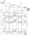
도 1은 본 발명의 실시예에 의한 유기전계발광 표시장치를 나타내는 도면이다.
도 2는 도 1에 도시된 화소의 실시예를 나타내는 도면이다.
도 3은 도 2에 도시된 화소의 구동방법을 나타내는 파형도이다.
도 4는 도 1에 도시된 화소의 다른 실시예를 나타내는 도면이다.
도 5는 도 4에 도시된 화소의 구동방법을 나타내는 파형도이다.
도 6은 본 발명의 다른 실시예에 의한 유기전계발광 표시장치를 나타내는 도면이다.1 is a diagram illustrating an organic light emitting display device according to an exemplary embodiment of the present invention.
FIG. 2 is a diagram illustrating an embodiment of a pixel illustrated in FIG. 1.
3 is a waveform diagram illustrating a method of driving the pixel illustrated in FIG. 2.
4 is a diagram illustrating another embodiment of the pixel illustrated in FIG. 1.
FIG. 5 is a waveform diagram illustrating a method of driving the pixel illustrated in FIG. 4.
6 is a diagram illustrating an organic light emitting display device according to another exemplary embodiment of the present invention.
이하, 본 발명이 속하는 기술분야에서 통상의 지식을 가진 자가 본 발명을 용이하게 실시할 수 있는 바람직한 실시 예가 첨부된 도 1 내지 도 6을 참조하여 자세히 설명하면 다음과 같다.
Hereinafter, the present invention will be described in detail with reference to FIGS. 1 to 6, which are attached to a preferred embodiment for easily carrying out the present invention by those skilled in the art.
도 1은 본 발명의 제 1실시예에 의한 유기전계발광 표시장치를 나타내는 도면이다.1 is a diagram illustrating an organic light emitting display device according to a first embodiment of the present invention.
도 1을 참조하면, 본 발명의 제 1실시예에 의한 유기전계발광 표시장치는 제 1주사선들(S1 내지 Sn) 및 데이터선들(D1 내지 Dm)의 교차부에 위치되는 화소들(140)을 포함하는 화소부(130)와, 제 1주사선들(S1 내지 Sn) 및 제 2주사선들(/S1 내지 /Sn)을 구동하기 위한 주사 구동부(110)와, 데이터선들(D1 내지 Dm)을 구동하기 위한 데이터 구동부(120)와, 주사 구동부(110) 및 데이터 구동부(120)를 제어하기 위한 타이밍 제어부(150)를 구비한다.Referring to FIG. 1, an organic light emitting display device according to a first exemplary embodiment of the present invention includes
또한, 본 발명의 실시예에 의한 유기전계발광 표시장치는 데이터선들(D1 내지 Dm)과 나란하게 수직라인마다 형성되어 화소들(140)과 접속되는 제 1전원선들(160)과, 주사선들(S1 내지 Sn)과 나란하게 수평라인마다 형성되어 화소들(140)과 접속되는 수평 전원선들(170)과, 화소부(130)의 외부에 제 2전원(ELVDD2)과 접속되게 형성되는 제 2전원선(180)과, 화소부(130)의 내부에 데이터선(Dm)과 나란하게 하나 이상 형성됨과 아울러 제 3전원(ELVDD3)과 접속되는 제 3전원선(190)과, 수평 전원선들(170) 각각과 제 2전원선(180) 사이에 형성되는 제 1스위칭소자(SW1)와, 수평 전원선(170) 각각과 제 3전원선(190) 사이에 접속되는 제 2스위칭소자(SW2)를 더 구비한다.In addition, the organic light emitting display device according to an exemplary embodiment of the present invention includes
주사 구동부(110)는 제 1주사선들(S1 내지 Sn)로 주사신호를 순차적으로 공급하고, 제 2주사선들(/S1 내지 /Sn)로 반전 주사신호를 순차적으로 공급한다. 주사신호는 화소(140)에 포함되는 트랜지스터들이 턴-온될 수 있는 전압(예를 들면, 로우레벨)으로 설정된다. 반전 주사신호는 인버터 등을 이용하여 주사신호의 극성을 반전한 신호로 트랜지스터가 턴-오프될 수 있는 전압으로 설정된다.The
예를 들어, i번째 제 2주사선(/Si)으로 공급되는 반전 주사신호는 i번째 제 1주사선(Si)으로 공급되는 주사신호를 반전하여 생성될 수 있다. 이 경우, i번째 제 2주사선(/Si)으로 공급되는 반전 주사신호는 극성만 반전될 뿐 i번째 제 1주사선(Si)으로 공급되는 주사신호와 동일한 공급시점 및 폭으로 설정된다.For example, the inverted scan signal supplied to the i-th second scan line / Si may be generated by inverting the scan signal supplied to the i-th first scan line Si. In this case, the inverted scan signal supplied to the i-th second scan line / Si is inverted in polarity and is set to the same supply time and width as the scan signal supplied to the i-th first scan line Si.
데이터 구동부(120)는 주사신호가 공급될 때 데이터선들(D1 내지 Dm)로 데이터신호를 공급한다.The
타이밍 제어부(150)는 주사 구동부(110) 및 데이터 구동부(120)를 제어한다. 또한, 타이밍 제어부(150)는 외부로부터 공급되는 데이터를 재정렬하여 데이터 구동부(120)로 전달한다.The
제 1전원선들(160)은 수직라인 단위로 화소들(140)과 접속되도록 형성된다. 이와 같은 제 1전원선들(160)은 제 1전원(ELVDD1)과 접속되며, 제 1전원(ELVDD1)의 전압을 화소들(140)로 공급한다. 제 1전원(ELVDD1)은 화소들(140) 각각에 포함되는 유기 발광 다이오드로 소정의 전류를 공급한다.The
제 2전원선(180)은 화소부(130)의 외부에 형성되며, 제 2전원(ELVDD2)과 접속된다. 제 2전원(ELVDD2)은 스토리지 커패시터에 전압이 충전된 후 화소(140)들 각각에 포함된 구동 트랜지스터의 게이트전극 전압을 제어하는 전원으로 데이터신호보다 낮은 전압으로 설정된다.The
제 3전원선(180)은 화소부(130)의 내부에 적어도 하나 이상 형성되며, 제 3전원(ELVDD3)과 접속된다. 제 3전원(ELVDD3)은 스토리지 커패시터에 충전되는 전압을 제어하는 전원으로 제 2전원(ELVDD2)보다 낮은 전압으로 설정된다.At least one
수평 전원선들(170)은 수평라인 단위로 화소들(140)과 접속된다. 이와 같은 수평 전원선들(170)은 제 1스위칭소자(SW1)가 턴-온되었을 때 제 2전원(ELVDD2)의 전압을 공급받고, 제 2스위칭소자(SW2)가 턴-온되었을 때 제 3전원(ELVDD3)의 전압을 공급받는다. 이를 위하여, 제 1스위칭소자(SW1) 및 제 2스위칭소자(SW2)는 교번적으로 턴-온 및 턴-오프를 반복한다.The
제 1스위칭소자(SW1)는 수평 전원선(170) 각각과 제 2전원선(180) 사이에 접속된다. 이와 같은 제 1스위칭소자(SW1)는 반전 주사신호가 공급될 때 턴-오프되고, 그 외의 기간 동안 턴-온된다.The first switching device SW1 is connected between each of the
제 2스위칭소자(SW2)는 수평 전원선(170) 각각과 제 3전원선(190) 사이에 접속된다. 이와 같은 제 2스위칭소자(SW2)는 주사신호가 공급될 때 턴-온되어 수평 전원선(170)과 제 3전원선(190)을 전기적으로 접속시킨다.The second switching element SW2 is connected between each of the
화소부(130)는 주사선들(S1 내지 Sn) 및 데이터선들(D1 내지 Dm)의 교차부에 위치되는 화소들(140)을 구비한다. 화소들(140) 각각에 포함되는 스토리지 커패시터는 데이터신호와 제 3전원(ELVDD3)의 전압차에 대응하는 전압을 충전한다. 여기서, 스토리지 커패시터는 데이터신호와 제 3전원(ELVDD3)에 대응하는 전압을 충전하고, 제 2전원(ELVDD2)의 전압에 대응하여 구동 트랜지스터의 게이트전극 전압을 제어한다. 구동 트랜지스터는 자신의 게이트전극에 인가된 전압에 대응하여 제 1전원(ELVDD1)으로부터 유기 발광 다이오드를 경유하여 제 4전원(ELVSS)으로 흐르는 전류량을 제어한다.
The
도 2는 도 1에 도시된 화소의 실시예를 나타내는 도면이다.FIG. 2 is a diagram illustrating an embodiment of a pixel illustrated in FIG. 1.
도 2를 참조하면, 본 발명의 실시예에 의한 화소(140)는 유기 발광 다이오드(OLED)와, 유기 발광 다이오드(OLED)로 공급되는 전류량을 제어하는 화소회로(142)와, 화소회로(142)와 수평 전원선(170) 사이에 접속되는 스토리지 커패시터(Cst)를 구비한다.2, a
유기 발광 다이오드(OLED)의 애노드전극은 화소회로(142)에 접속되고, 캐소드전극은 제 4전원(ELVSS)에 접속된다. 이와 같은 유기 발광 다이오드(OLED)는 화소회로(142)로부터 공급되는 전류에 대응하여 소정 휘도의 빛을 생성한다.The anode electrode of the organic light emitting diode OLED is connected to the
스토리지 커패시터(Cst)는 구동 트랜지스터(즉, 제 1트랜지스터(M1))의 게이트전극과 수평 전원선(170) 사이에 접속된다. 이와 같은 스토리지 커패시터(Cst)는 화소회로(142)로부터 공급되는 데이터신호와 수평 전원선(170)으로부터 공급되는 제 3전원(ELVDD3)에 대응하는 전압을 충전한다. 그리고, 스토리지 커패시터(Cst)는 소정의 전압이 충전된 이후에 수평 전원선(170)으로 공급되는 제 2전원(ELVDD2)에 대응하여 구동 트랜지스터의 게이트전극 전압을 제어한다.The storage capacitor Cst is connected between the gate electrode of the driving transistor (ie, the first transistor M1) and the horizontal
화소회로(142)는 스토리지 커패시터(Cst)에 충전된 전압에 대응하여 제 1전원(ELVDD1)으로부터 유기 발광 다이오드(OLED)를 경유하여 제 4전원(ELVSS)으로 흐르는 전류량을 제어한다. 이를 위하여, 화소회로(142)는 제 1트랜지스터(M1) 및 제 2트랜지스터(M2)를 구비한다.The
제 1트랜지스터(M1)의 제 1전극은 제 1전원선(160)을 경유하여 제 1전원(ELVDD1)에 접속되고, 제 2전극은 유기 발광 다이오드(OLED)의 애노드전극에 접속된다. 그리고, 제 1트랜지스터(M1)의 게이트전극은 스토리지 커패시터(Cst)의 제 1단자에 접속된다. 이와 같은 제 1트랜지스터(M1)는 스토리지 커패시터(Cst)에 충전된 전압에 대응하여 유기 발광 다이오드(OLED)로 공급되는 전류량을 제어한다.The first electrode of the first transistor M1 is connected to the first power supply ELVDD1 via the first
제 2트랜지스터(M2)의 제 1전극은 데이터선(Dm)에 접속되고, 제 2전극은 제 1트랜지스터(M1)의 게이트전극에 접속된다. 그리고, 제 2트랜지스터(M2)의 게이트전극은 제 1주사선(Sn)에 접속된다. 이와 같은 제 2트랜지스터(M2)는 제 1주사선(Sn)으로 주사신호가 공급될 때 턴-온되어 데이터선(Dm)과 제 1트랜지스터(M1)의 게이트전극을 전기적으로 접속시킨다.
The first electrode of the second transistor M2 is connected to the data line Dm, and the second electrode is connected to the gate electrode of the first transistor M1. The gate electrode of the second transistor M2 is connected to the first scan line Sn. The second transistor M2 is turned on when the scan signal is supplied to the first scan line Sn to electrically connect the data line Dm and the gate electrode of the first transistor M1.
도 3은 도 2에 도시된 화소의 구동방법을 나타내는 파형도이다.3 is a waveform diagram illustrating a method of driving the pixel illustrated in FIG. 2.
도 3을 참조하면, 먼저 제 1주사선(Sn)으로 주사신호가 공급되고, 제 2주사선(/Sn)으로 반전 주사신호가 공급된다.Referring to FIG. 3, a scan signal is first supplied to the first scan line Sn, and an inverted scan signal is supplied to the second scan line / Sn.
제 2주사선(/Sn)으로 반전 주사신호가 공급되면 제 1스위칭소자(SW1)가 턴-오프된다. 제 1스위칭소자(SW1)가 턴-오프되면 수평 전원선(170)과 제 2전원선(180)이 전기적으로 차단된다.When the inverted scan signal is supplied to the second scan line / Sn, the first switching device SW1 is turned off. When the first switching device SW1 is turned off, the
제 1주사선(Sn)으로 주사신호가 공급되면 제 2스위칭소자(SW2) 및 제 2트랜지스터(M2)가 턴-온된다. 제 2스위칭소자(SW2)가 턴-온되면 수평 전원선(170)과 제 3전원선(190)이 전기적으로 접속된다. 이 경우, 수평 전원선(170)으로는 제 3전원(ELVDD3)의 전압이 공급된다.When the scan signal is supplied to the first scan line Sn, the second switching device SW2 and the second transistor M2 are turned on. When the second switching device SW2 is turned on, the horizontal
제 2트랜지스터(M2)가 턴-온되면 데이터선(Dm)과 제 1트랜지스터(M1)의 게이트전극이 전기적으로 접속된다. 따라서, 데이터선(Dm)으로부터의 데이터신호가 제 1트랜지스터(M1)의 게이트전극으로 공급된다. 이때, 스토리지 커패시터(Cst)는 데이터신호 및 제 3전원(ELVDD3)의 차에 대응하는 전압을 충전한다.When the second transistor M2 is turned on, the data line Dm and the gate electrode of the first transistor M1 are electrically connected to each other. Therefore, the data signal from the data line Dm is supplied to the gate electrode of the first transistor M1. In this case, the storage capacitor Cst charges a voltage corresponding to the difference between the data signal and the third power source ELVDD3.
스토리지 커패시터(Cst)에 전압이 충전된 이후에 제 1주사선(Sn)으로 주사신호의 공급이 중단되고, 제 2주사선(/Sn)으로 반전 주사신호의 공급이 중단된다. 제 1주사선(Sn)으로 주사신호의 공급이 중단되면 제 2트랜지스터(M2) 및 제 2스위칭소자(SW2)가 턴-오프된다.After the voltage is charged in the storage capacitor Cst, the supply of the scan signal to the first scan line Sn is stopped and the supply of the inverted scan signal to the second scan line / Sn is stopped. When the supply of the scan signal to the first scan line Sn is stopped, the second transistor M2 and the second switching device SW2 are turned off.
제 2주사선(/Sn)으로 반전 주사신호의 공급이 중단되면 제 1스위칭소자(SW1)가 턴-온된다. 제 1스위칭소자(SW1)가 턴-온되면 제 2전원선(180)과 수평 전원선(170)이 전기적으로 접속되고, 이에 따라 수평 전원선(170)으로 제 2전원(ELVDD2)의 전압이 공급된다.When the supply of the inverted scan signal to the second scan line / Sn is stopped, the first switching device SW1 is turned on. When the first switching device SW1 is turned on, the
이때, 수평 전원선(170)의 전압은 제 3전원(ELVDD3)의 전압으로부터 제 2전원(ELVDD2)의 전압으로 상승한다. 수평 전원선(170)의 전압이 상승하면 스토리지 커패시터(Cst)에 의하여 제 1트랜지스터(M1)의 게이트전극 전압도 상승한다. 이와 같이 스토리지 커패시터(Cst)에 의하여 게이트전극 전압이 상승하면 원하는 휘도의 영상을 표시할 수 있다. 다시 말하여, 데이터선(Dm)의 기생 커패시터와 스토리지 커패시터(Cst)의 차지 쉐어링에 의하여 손실된 데이터신호의 전압만큼 제 1트랜지스터(M1)의 게이트전극 전압을 상승시키고, 이에 따라 원하는 휘도의 영상을 표시할 수 있다. 이를 위하여, 제 2전원(ELVDD2) 및 제 3전원(ELVDD3)의 차전압은 차지 쉐어링에 의하여 손실된 데이터신호의 전압이 보상될 수 있도록 실험적으로 결정된다.At this time, the voltage of the horizontal
제 1트랜지스터(M1)의 게이트전극 전압이 상승한 후 제 1트랜지스터(M1)는 자신의 게이트전극에 인가된 전압에 대응하여 제 1전원(ELVDD1)으로부터 유기 발광 다이오드(OLED)를 경유하여 제 4전원(ELVSS)으로 흐르는 전류량을 제어한다.After the gate electrode voltage of the first transistor M1 rises, the first transistor M1 corresponds to the voltage applied to its gate electrode, and thus, the fourth transistor M4 passes through the organic light emitting diode OLED from the first power source ELVDD1. Control the amount of current flowing to ELVSS.
이와 같은 본원 발명에서 스토리지 커패시터(Cst)에 충전되는 전압은 유기 발광 다이오드(OLED)로 전류를 공급하는 제 1전원(ELVDD1)과 무관하게 결정된다. 다시 말하여, 본원 발명에서는 전압강하가 발생되지 않는 제 3전원(ELVDD3)을 이용하여 스토리지 커패시터(Cst)에 전압을 충전하고, 이에 따라 원하는 휘도의 영상을 표시할 수 있다.In the present invention, the voltage charged in the storage capacitor Cst is determined irrespective of the first power source ELVDD1 supplying a current to the organic light emitting diode OLED. In other words, in the present invention, the voltage is charged in the storage capacitor Cst by using the third power source ELVDD3 which does not generate a voltage drop, thereby displaying an image having a desired luminance.
한편, 본 발명에서 스토리지 커패시터(Cst)는 MOS 커패시터(Cst)로 형성되고, 이에 따라 제조비용을 줄일 수 있는 장점이 있다.Meanwhile, in the present invention, the storage capacitor Cst is formed of the MOS capacitor Cst, thereby reducing the manufacturing cost.
상세히 설명하면, 상세히 설명하면, 일반적으로 스토리지 커패시터(Cst)는 폴리(poly)를 결정화하여 금속처리하고, 금속 처리된 폴리(poly)와 게이트금속(Metal Cap) 사이의 중첩면적을 이용하여 전압을 저장한다.(용량을 늘리기 위하여 게이트금속과 소스/드레인금속 사이의 중첩면적을 추가로 이용하기도 한다.) 하지만, 폴리(poly)를 결정화하기 위하여 공정과정에서 마스크가 추가되고, 이에 따라 제조비용이 증가하는 문제점이 발생한다.In detail, in detail, the storage capacitor Cst is generally metallized by crystallization of poly, and voltages are obtained by using an overlapping area between the metallized poly and the gate metal. (An additional overlap between the gate metal and the source / drain metal may be used to increase capacity.) However, a mask is added during the process to crystallize the poly, thereby increasing the manufacturing cost. An increasing problem arises.
하지만, 본 발명에서는 폴리(Poly)와 게이트금속(MOS Cap) 사이의 중첩면적을 이용하여 스토리지 커패시터(Cst)를 형성한다.(용량을 늘리기 위하여 게이트금속과 소스/드레인금속 사이의 중첩면적을 추가로 이용할 수 있다.) 이 경우, 폴리(poly)를 결정화하기 위한 마스크가 제거되어 제조비용을 절감할 수 있다.However, in the present invention, the storage capacitor Cst is formed using the overlapping area between poly and the gate metal (MOS Cap). (To increase the capacity, the overlapping area between the gate metal and the source / drain metal is added. In this case, the mask for crystallizing the poly (poly) is removed to reduce the manufacturing cost.
여기서, 스토리지 커패시터(Cst)의 게이트금속은 제 2단자로서 수평 전원선(170)에 접속되고, 폴리는 제 1단자로서 제 1트랜지스터(M1)의 게이트전극에 접속된다. 그리고, 스토리지 커패시터(Cst)가 안정적으로 전압을 충전할 수 있도록 제 2전원(ELVDD2) 및 제 3전원(ELVDD3)의 전압은 데이터신호의 전압보다 낮은 전압으로 설정된다.
Here, the gate metal of the storage capacitor Cst is connected to the horizontal
도 4는 도 2에 도시된 화소의 다른 실시예를 나타내는 도면이다. 도 4를 설명할 때 도 2와 동일한 구성에 대해서는 동일한 도면부호를 할당함과 아울러 상세한 설명은 생략하기로 한다.FIG. 4 is a diagram illustrating another embodiment of the pixel illustrated in FIG. 2. 4, the same components as those in FIG. 2 are assigned the same reference numerals, and detailed description thereof will be omitted.
도 4를 참조하면, 본 발명의 다른 실시예에 의한 화소(140)는 유기 발광 다이오드(OLED) 및 스토리지 커패시터(Cst)와, 스토리지 커패시터(Cst)에 충전된 전압에 대응하여 유기 발광 다이오드(OLED)로 공급되는 전류량을 제어하는 화소회로(142')를 구비한다.Referring to FIG. 4, the
유기 발광 다이오드(OLED)의 애노드전극은 화소회로(142')에 접속되고, 캐소드전극은 제 4전원(ELVSS)에 접속된다. 이와 같은 유기 발광 다이오드(OLED)는 화소회로(142')로부터 공급되는 전류에 대응하여 소정 휘도의 빛을 생성한다.The anode electrode of the organic light emitting diode OLED is connected to the pixel circuit 142 ', and the cathode electrode is connected to the fourth power source ELVSS. The organic light emitting diode OLED generates light having a predetermined luminance in response to a current supplied from the pixel circuit 142 '.
스토리지 커패시터(Cst)는 MOS 커패시터로 형성되며, 제 1트랜지스터(M1)의 게이트전극과 수평 전원선(170) 사이에 접속된다. 이와 같은 스토리지 커패시터(Cst)는 데이터신호와 제 3전원(ELVDD3)에 대응하는 전압을 충전한다. 그리고, 스토리지 커패시터(Cst)는 수평 전원선(170)으로 공급되는 제 2전원(ELVDD2)에 대응하여 구동 트랜지스터의 게이트전극 전압을 제어한다.The storage capacitor Cst is formed of a MOS capacitor and is connected between the gate electrode of the first transistor M1 and the horizontal
화소회로(142')는 스토리지 커패시터(Cst)에 충전된 전압에 대응하여 제 1전원(ELVDD1)으로부터 유기 발광 다이오드(OLED)를 경유하여 제 4전원(ELVSS)으로 흐르는 전류량을 제어한다. 이를 위하여, 화소회로(142')는 제 1 내지 제 6트랜지스터(M1 내지 M6)를 구비한다.The
제 1트랜지스터(M1)의 제 1전극은 제 5트랜지스터(M5)의 제 2전극에 접속되고, 제 2전극은 제 6트랜지스터(M6)의 제 1전극에 접속된다. 그리고, 제 1트랜지스터(M1)의 게이트전극은 스토리지 커패시터(Cst)의 제 1단자에 접속된다. 이와 같은 제 1트랜지스터(M1)는 자신의 게이트전극에 인가된 전압에 대응하는 전류를 유기 발광 다이오드(OLED)로 공급한다.The first electrode of the first transistor M1 is connected to the second electrode of the fifth transistor M5, and the second electrode is connected to the first electrode of the sixth transistor M6. The gate electrode of the first transistor M1 is connected to the first terminal of the storage capacitor Cst. The first transistor M1 supplies a current corresponding to the voltage applied to its gate electrode to the organic light emitting diode OLED.
제 2트랜지스터(M2)의 제 1전극은 데이터선(Dm)에 접속되고, 제 2전극은 제 1트랜지스터(M1)의 제 1전극에 접속된다. 그리고, 제 2트랜지스터(M2)의 게이트전극은 n번째 제 1주사선(Sn)에 접속된다. 이와 같은 제 2트랜지스터(M2)는 n번째 제 1주사선(Sn)으로 주사신호가 공급될 때 턴-온되어 데이터선(Dm)과 제 1트랜지스터(M1)의 제 1전극을 전기적으로 접속시킨다.The first electrode of the second transistor M2 is connected to the data line Dm, and the second electrode is connected to the first electrode of the first transistor M1. The gate electrode of the second transistor M2 is connected to the nth first scan line Sn. The second transistor M2 is turned on when the scan signal is supplied to the n-th first scan line Sn to electrically connect the data line Dm and the first electrode of the first transistor M1.
제 3트랜지스터(M3)의 제 1전극은 제 1트랜지스터(M1)의 제 2전극에 접속되고, 제 2전극은 제 1트랜지스터(M1)의 게이트전극에 접속된다. 그리고, 제 3트랜지스터(M3)의 게이트전극은 n번째 제 1주사선(Sn)에 접속된다. 이와 같은 제 3트랜지스터(M3)는 n번째 제 1주사선(Sn)으로 주사신호가 공급될 때 턴-온되어 제 1트랜지스터(M1)를 다이오드 형태로 접속시킨다.The first electrode of the third transistor M3 is connected to the second electrode of the first transistor M1, and the second electrode is connected to the gate electrode of the first transistor M1. The gate electrode of the third transistor M3 is connected to the nth first scan line Sn. The third transistor M3 is turned on when the scan signal is supplied to the n-th first scan line Sn to connect the first transistor M1 in the form of a diode.
제 4트랜지스터(M4)의 제 1전극은 제 1트랜지스터(M1)의 게이트전극에 접속되고, 제 2전극은 수평 전원선(170)에 접속된다. 그리고, 제 4트랜지스터(M4)의 게이트전극은 n-1번째 제 1주사선(Sn-1)에 접속된다. 이와 같은 제 4트랜지스터(M4)는 n-1번째 제 1주사선(Sn-1)으로 주사신호가 공급될 때 턴-온되어 수평 전원선(170)과 제 1트랜지스터(M1)의 게이트전극을 전기적으로 접속시킨다.The first electrode of the fourth transistor M4 is connected to the gate electrode of the first transistor M1, and the second electrode is connected to the horizontal
제 5트랜지스터(M5)의 제 1전극은 제 1전원선(160)을 경유하여 제 1전원(ELVDD1)에 접속되고, 제 2전극은 제 1트랜지스터(M1)의 제 1전극에 접속된다. 그리고, 제 5트랜지스터(M5)의 게이트전극은 발광 제어선(En)에 접속된다. 이와 같은 제 5트랜지스터(M5)는 발광 제어선(En)으로 발광 제어신호가 공급될 때 턴-오프되고, 그 외의 기간 동안 턴-온된다.The first electrode of the fifth transistor M5 is connected to the first power supply ELVDD1 via the first
제 6트랜지스터(M6)의 제 1전극은 제 1트랜지스터(M1)의 제 2전극에 접속되고, 제 2전극은 유기 발광 다이오드(OLED)의 애노드전극에 접속된다. 그리고, 제 6트랜지스터(M6)의 게이트전극은 발광 제어선(En)에 접속된다. 이와 같은 제 6트랜지스터(M6)는 발광 제어선(En)으로 발광 제어신호가 공급될 때 턴-오프되고, 그 외의 기간 동안 턴-온된다.The first electrode of the sixth transistor M6 is connected to the second electrode of the first transistor M1, and the second electrode is connected to the anode electrode of the organic light emitting diode OLED. The gate electrode of the sixth transistor M6 is connected to the emission control line En. The sixth transistor M6 is turned off when the emission control signal is supplied to the emission control line En, and is turned on for the other period.
한편, 발광 제어선은 도 6에 도시된 바와 같이 제 1주사선들(S1 내지 Sn)과 나라한게 수평라인마다 형성된다. 그리고, i(i는 자연수)번째 발광 제어선(Ei)으로 공급되는 발광 제어신호는 i-1 및 i번째 제 1주사선(Si-1, Si)으로 공급되는 주사신호와 중첩되게 공급된다.
Meanwhile, as illustrated in FIG. 6, the emission control line is formed for each horizontal line with the first scan lines S1 to Sn. The light emission control signal supplied to the i (i is a natural number) th light emission control line Ei is supplied to overlap with the scan signals supplied to the i-1 and i th scan lines Si-1 and Si.
도 5는 도 4에 도시된 화소의 구동방법을 나타내는 파형도이다.FIG. 5 is a waveform diagram illustrating a method of driving the pixel illustrated in FIG. 4.
도 5를 참조하면, 먼저 발광 제어선(En)으로 발광 제어신호가 공급된다. 발광 제어선(En)으로 발광 제어신호가 공급되면 제 5트랜지스터(M5) 및 제 6트랜지스터(M6)가 턴-오프된다. 제 5트랜지스터(M5) 및 제 6트랜지스터(M6)가 턴-오프되면 제 1트랜지스터(M1)가 제 1전원(ELVDD1) 및 유기 발광 다이오드(OLED)와 전기전으로 차단되고, 이에 따라 유기 발광 다이오드(OLED)가 비발광 상태로 설정된다.Referring to FIG. 5, an emission control signal is first supplied to an emission control line En. When the emission control signal is supplied to the emission control line En, the fifth transistor M5 and the sixth transistor M6 are turned off. When the fifth transistor M5 and the sixth transistor M6 are turned off, the first transistor M1 is cut off with the first power source ELVDD1 and the organic light emitting diode OLED, and accordingly, the organic light emitting diode (OLED) is set to the non-luminescing state.
이후, n-1번째 제 1주사선(Sn-1)으로 주사신호가 공급되어 제 4트랜지스터(M4)가 턴-온된다. 제 4트랜지스터(M4)가 턴-온되면 제 1트랜지스터(M1)의 게이트전극과 수평 전원선(170)이 전기적으로 접속된다. 이때, 제 1트랜지스터(M1)의 게이트전극은 수평 전원선(170)으로 공급되는 제 2전원(ELVDD2)의 전압으로 초기화된다.Thereafter, the scan signal is supplied to the n−1 th first scan line Sn−1 so that the fourth transistor M4 is turned on. When the fourth transistor M4 is turned on, the gate electrode of the first transistor M1 and the horizontal
제 1트랜지스터(M1)의 게이트전극이 제 2전원(ELVDD2)의 전압으로 초기화된 후 n번째 제 1주사선(Sn)으로 주사신호가 공급되어 제 2스위칭소자(SW2), 제 2트랜지스터(M2) 및 제 3트랜지스터(M3)가 턴-온된다. 그리고, n번째 제 2주사선(/Sn)으로 반전 주사신호가 공급되어 제 1스위칭소자(SW1)가 턴-오프된다.After the gate electrode of the first transistor M1 is initialized to the voltage of the second power source ELVDD2, a scan signal is supplied to the nth first scan line Sn to supply the second switching device SW2 and the second transistor M2. And the third transistor M3 is turned on. The inverted scan signal is supplied to the n-th second scan line / Sn to turn off the first switching device SW1.
제 3트랜지스터(M3)가 턴-온되면 제 1트랜지스터(M1)가 다이오드 형태로 접속된다.When the third transistor M3 is turned on, the first transistor M1 is connected in the form of a diode.
제 2트랜지스터(M2)가 턴-온되면 데이터선(Dm)으로부터의 데이터신호가 제 1트랜지스터(M1)의 제 1전극으로 공급된다. 이때, 제 1트랜지스터(M1)의 게이트전극이 데이터신호보다 낮은 전압을 가지는 제 2전원(ELVDD2)으로 초기화되었기 때문에 데이터신호는 제 1트랜지스터(M1)의 게이트전극으로 공급된다. 이 경우, 제 1트랜지스터(M1)의 게이트전극으로 공급되는 데이터신호는 데이터신호의 전압에서 제 1트랜지스터(M1)의 절대치 문턱전압을 감한 전압으로 설정된다.When the second transistor M2 is turned on, the data signal from the data line Dm is supplied to the first electrode of the first transistor M1. At this time, since the gate electrode of the first transistor M1 is initialized to the second power source ELVDD2 having a lower voltage than the data signal, the data signal is supplied to the gate electrode of the first transistor M1. In this case, the data signal supplied to the gate electrode of the first transistor M1 is set to a voltage obtained by subtracting the absolute threshold voltage of the first transistor M1 from the voltage of the data signal.
제 2스위칭소자(SW2)가 턴-온되면 제 3전원(ELVDD3)의 전압이 수평 전원선(170)으로 공급된다. 이때, 스토리지 커패시터(Cst)는 제 1트랜지스터(M1)의 게이트전극에 인가된 데이터시호와 제 3전원(ELVDD3)의 차에 해당하는 전압을 충전한다.When the second switching device SW2 is turned on, the voltage of the third power supply ELVDD3 is supplied to the horizontal
이후, 제 n번째 제 1주사선(Sn)으로 주사신호의 공급이 중단되어 제 2스위치소자(SW2), 제 2트랜지스터(M2) 및 제 3트랜지스터(M3)가 턴-오프된다. 그리고, n번째 제 2주사선(/Sn)으로 반전 주사신호의 공급이 중단되어 수평 전원선(170)으로 제 2전원(ELVDD2)의 전압이 공급된다. 이때, 스토리지 커패시터(Cst)는 제 3전원(ELVDD3)과 제 2전원(ELVDD2)의 차에 해당하는 전압만큼 제 1트랜지스터(M1)의 게이트전극 전압을 상승시킨다.Thereafter, the supply of the scan signal to the nth first scan line Sn is stopped to turn off the second switch element SW2, the second transistor M2, and the third transistor M3. Then, the supply of the inverted scan signal to the n-th second scan line / Sn is stopped, and the voltage of the second power source ELVDD2 is supplied to the horizontal
제 1트랜지스터(M1)의 게이트전극 전압이 상승된 이후에 발광 제어선(En)으로 발광 제어신호의 공급이 중단된다. 발광 제어선(En)으로 발광 제어신호의 공급이 중단되면 제 5트랜지스터(M5) 및 제 6트랜지스터(M6)가 턴-온된다.After the gate electrode voltage of the first transistor M1 is increased, the supply of the emission control signal to the emission control line En is stopped. When the supply of the emission control signal to the emission control line En is stopped, the fifth transistor M5 and the sixth transistor M6 are turned on.
제 5트랜지스터(M5)가 턴-온되면 제 1전원(ELVDD1)과 제 1트랜지스터(M1)의 제 1전극이 전기적으로 접속된다. 제 6트랜지스터(M6)가 턴-온되면 유기 발광 다이오드(OLED)의 애노드전극과 제 1트랜지스터(M1)의 제 2전극이 전기적으로 접속된다. 이 경우, 제 1트랜지스터(M1)는 자신의 게이트전극에 인가된 전압에 대응하여 제 1전원(ELVDD1)으로부터 유기 발광 다이오드(OLED)를 경유하여 제 4전원(ELVSS)으로 흐르는 전류량을 제어한다.When the fifth transistor M5 is turned on, the first power source ELVDD1 and the first electrode of the first transistor M1 are electrically connected to each other. When the sixth transistor M6 is turned on, the anode electrode of the organic light emitting diode OLED and the second electrode of the first transistor M1 are electrically connected to each other. In this case, the first transistor M1 controls the amount of current flowing from the first power source ELVDD1 to the fourth power source ELVSS via the organic light emitting diode OLED in response to the voltage applied to its gate electrode.
한편, 도 1에서는 수평라인마다 하나의 제 2스위칭소자(SW2)가 형성되는 것으로 도시되었지만 본원 발명이 이에 한정되지는 않는다. 예를 들어, 도 6에 도시된 바와 같이 수평 전원선(170) 각각과 제 3전원선(190) 사이에 접속되는 제 3스위칭소자(SW3)를 더 구비할 수 있다.In FIG. 1, one second switching device SW2 is formed for each horizontal line, but the present invention is not limited thereto. For example, as illustrated in FIG. 6, a third switching device SW3 may be further connected between each of the
i번째 수평라인에 위치된 제 3스위칭소자(SW3)는 i-1번째 제 1주사선(Si-1)으로 주사신호가 공급될 때 턴-온되어 제 3전원선(190)과 수평 전원선(170)을 전기적으로 접속한다. 이와 같은 구성이 도 4에 도시된 화소(140)에 적용되는 경우 제 1트랜지스터(M1)의 게이트전극은 제 3전원(ELVDD3)의 전압에 의하여 초기화된다.The third switching element SW3 positioned in the i-th horizontal line is turned on when the scan signal is supplied to the i-th first scan line Si-1, so that the
본 발명의 기술 사상은 상기 바람직한 실시예에 따라 구체적으로 기술되었으나, 상기한 실시예는 그 설명을 위한 것이며 그 제한을 위한 것이 아님을 주의하여야 한다. 또한, 본 발명의 기술 분야의 통상의 지식을 가진 자라면 본 발명의 기술 사상의 범위 내에서 다양한 변형예가 가능함을 이해할 수 있을 것이다.
Although the technical idea of the present invention has been described in detail according to the above preferred embodiment, it should be noted that the above-described embodiment is for the purpose of description and not of limitation. In addition, those skilled in the art will understand that various modifications are possible within the scope of the technical idea of the present invention.
110 : 주사 구동부120 : 데이터 구동부
130 : 화소부140 : 화소
142 : 화소회로150 : 타이밍 제어부
160,170,180,190 : 전원선110: scan driver 120: data driver
130: pixel portion 140: pixel
142: pixel circuit 150: timing controller
160,170,180,190: power line
Claims (14)
Translated fromKorean데이터선들로 데이터신호를 공급하는 데이터 구동부와;
상기 제 1주사선들 및 데이터선들의 교차부에 위치되는 화소들을 포함하는 화소부와;
제 1전원과 접속되며 수직라인 단위로 상기 화소들과 접속되는 제 1전원선들과;
상기 화소부의 외부에 형성되며 상기 제 1전원과 상이한 전압을 가지는 제 2전원과 접속되는 제 2전원선과;
상기 데이터선과 나란하게 하나 이상 형성되며 상기 제 1전원과 상이한 전압을 가지는 제 3전원과 접속되는 제 3전원선과;
상기 주사선들과 나란하게 수평라인 단위로 형성되어 상기 화소들과 접속되는 수평 전원선들을 구비하며;
상기 화소들 각각은 상기 데이터신호와 상기 제 3전원에 대응하는 전압을 충전하고, 충전된 전압에 대응하여 상기 제 1전원으로부터 흐르는 전류량을 제어하는 것을 특징으로 하는 유기전계발광 표시장치.A scan driver for sequentially supplying scan signals to the first scan lines and sequentially supplying inverted scan signals to the second scan lines;
A data driver for supplying a data signal to the data lines;
A pixel portion including pixels positioned at an intersection of the first scan lines and the data lines;
First power lines connected to a first power source and connected to the pixels in a vertical line unit;
A second power supply line formed outside the pixel portion and connected to a second power supply having a voltage different from that of the first power supply;
A third power line formed in parallel with the data line and connected to a third power source having a voltage different from that of the first power source;
Horizontal power lines formed parallel to the scan lines in horizontal line units to be connected to the pixels;
And each of the pixels charges a voltage corresponding to the data signal and the third power source, and controls an amount of current flowing from the first power source in response to the charged voltage.
상기 제 2전원은 상기 제 3전원보다 높은 전압으로 설정되는 것을 특징으로 하는 유기전계 발광표시장치.The method of claim 1,
And the second power supply is set to a higher voltage than the third power supply.
상기 제 2전원 및 제 3전원은 상기 데이터신호보다 낮은 전압으로 설정되는 것을 특징으로 하는 유기전계발광 표시장치.The method of claim 1,
And the second power source and the third power source are set at a voltage lower than that of the data signal.
상기 수평전원선들 각각과 상기 제 2전원선 사이에 접속되는 제 1스위칭소와,
상기 수평전원선들 각각과 상기 제 3전원선 사이에 접속되는 제 2스위칭소자를 더 구비하는 것을 특징으로 하는 유기전계발광 표시장치.The method of claim 1,
A first switching station connected between each of the horizontal power lines and the second power line;
And a second switching element connected between each of the horizontal power lines and the third power line.
상기 제 1스위칭소자 및 제 2스위칭소자는 서로 교번적으로 턴-온 및 턴-오프되는 것을 특징으로 하는 유기전계발광 표시장치.The method of claim 4, wherein
And the first switching element and the second switching element are alternately turned on and off.
i(i는 자연수)번째 수평라인에 위치된 제 1스위칭소자는 i번째 제 1주사선으로 주사신호가 공급될 때 턴-온되고, 상기 i번째 수평라인에 위치된 제 2스위칭소자는 i번째 제 2주사선으로 반전 주사신호가 공급될 때 턴-오프되고 그 외의 기간 동안 턴-온되는 것을 특징으로 하는 유기전계발광 표시장치.6. The method of claim 5,
The first switching element located on the i-th horizontal line is turned on when the scan signal is supplied to the i-th first scan line, and the second switching element located on the i-th horizontal line is the i-th An organic light emitting display device which is turned off when the inverted scan signal is supplied to two scan lines and turned on for another period.
상기 수평 전원선들 각각과 상기 제 3전원선 사이에 접속되는 제 3스위칭소자를 더 구비하는 것을 특징으로 하는 유기전계발광 표시장치.The method of claim 4, wherein
And a third switching element connected between each of the horizontal power lines and the third power line.
i(i는 자연수)번째 수평라인에 위치된 제 3스위칭소자는 i-1번째 제 1주사선으로 주사신호가 공급될 때 턴-온되는 것을 특징으로 하는 유기전계발광 표시장치.The method of claim 7, wherein
and the third switching element positioned on the i-th horizontal line is turned on when the scan signal is supplied to the i-th first scan line.
i(i는 자연수)번째 제 1주사선으로 공급되는 주사신호는 i번째 제 2주사선으로 공급되는 주사신호와 동일한 시점에 동일한 폭으로 공급되며, 서로 반전된 극성으로 설정되는 것을 특징으로 하는 유기전계발광 표시장치.The method of claim 1,
The organic light emitting diode is characterized in that the scan signal supplied to the i (i is a natural number) first scan line is supplied with the same width at the same time as the scan signal supplied to the i th second scan line and is set to be inverted polarity. Display.
제 i번째 수평라인에 위치된 화소들 각각은
유기 발광 다이오드와;
상기 유기 발광 다이오드와 상기 제 1전원선 사이에 접속되는 제 1트랜지스터와;
상기 제 1트랜지스터의 게이트전극과 상기 데이터선 사이에 접속되며, 상기 i번째 제 1주사선으로 주사신호가 공급될 때 턴-온되는 제 2트랜지스터와;
상기 제 1트랜지스터의 게이트전극과 상기 수평 전원선 사이에 접속되는 스토리지 커패시터를 구비하는 것을 특징으로 하는 유기전계발광 표시장치.The method of claim 9,
Each of the pixels located in the i th horizontal line
An organic light emitting diode;
A first transistor connected between the organic light emitting diode and the first power line;
A second transistor connected between the gate electrode of the first transistor and the data line and turned on when a scan signal is supplied to the i-th first scan line;
And a storage capacitor connected between the gate electrode of the first transistor and the horizontal power supply line.
상기 제 1주사선들과 나란하게 상기 수평라인마다 형성되는 발광 제어선들을 더 구비하는 것을 특징으로 하는 유기전계발광 표시장치.The method of claim 9,
And an emission control line formed in the horizontal line in parallel with the first scan lines.
상기 주사 구동부는 i-1번째 제 1주사선 및 i번째 제 1주사선으로 공급되는 제 1주사신호와 중첩되도록 i번째 발광 제어선으로 발광 제어신호를 공급하는 것을 특징으로 하는 유기전계발광 표시장치.12. The method of claim 11,
And the scan driver supplies a light emission control signal to the i th light emission control line to overlap the first scan signal supplied to the i-1 th first scan line and the i th first scan line.
제 i번째 수평라인에 위치된 화소들 각각은
유기 발광 다이오드와;
제 1전극이 상기 제 1전원선에 접속되고, 제 2전극이 상기 유기 발광 다이오드에 접속되는 제 1트랜지스터와;
상기 데이터선과 상기 제 1트랜지스터의 제 1전극 사이에 접속되며, 상기 i번째 제 1주사선으로 주사신호가 공급될 때 턴-온되는 제 2트랜지스터와;
상기 제 1트랜지스터의 게이트전극과 제 2전극 사이에 접속되며, 상기 i번째 제 1주사선으로 주사신호가 공급될 때 턴-온되는 제 3트랜지스터와;
상기 제 1트랜지스터의 게이트전극과 상기 수평 전원선 사이에 접속되며, 상기 i-1번째 제 1주사선으로 주사신호가 공급될 때 턴-온되는 제 4트랜지스터와;
상기 제 1트랜지스터의 게이트전극과 상기 수평 전원선 사이에 접속되는 스토리지 커패시터를 구비하는 것을 특징으로 하는 유기전계발광 표시장치.The method of claim 12,
Each of the pixels located in the i th horizontal line
An organic light emitting diode;
A first transistor having a first electrode connected to said first power line, and a second electrode connected to said organic light emitting diode;
A second transistor connected between the data line and the first electrode of the first transistor and turned on when a scan signal is supplied to the i-th first scan line;
A third transistor connected between the gate electrode and the second electrode of the first transistor and turned on when a scan signal is supplied to the i-th first scan line;
A fourth transistor connected between the gate electrode of the first transistor and the horizontal power supply line and turned on when a scan signal is supplied to the i-1th first scan line;
And a storage capacitor connected between the gate electrode of the first transistor and the horizontal power supply line.
상기 제 1트랜지스터의 제 1전극과 상기 제 1전원선 사이에 접속되며, 상기 i번째 발광 제어선으로 발광 제어신호가 공급될 때 턴-오프되는 제 5트랜지스터와;
상기 제 1트랜지스터의 제 2전극과 상기 유기 발광 다이오드 사이에 접속되며, 상기 i번째 발광 제어선으로 발광 제어신호가 공급될 대 턴-오프되는 제 6트랜지스터를 더 구비하는 것을 특징으로 하는 유기전계발광 표시장치.The method of claim 13,
A fifth transistor connected between the first electrode of the first transistor and the first power supply line and turned off when an emission control signal is supplied to the i-th emission control line;
And a sixth transistor connected between the second electrode of the first transistor and the organic light emitting diode and turned off when an emission control signal is supplied to the i th emission control line. Display.
Priority Applications (2)
| Application Number | Priority Date | Filing Date | Title |
|---|---|---|---|
| KR1020100043506AKR101093374B1 (en) | 2010-05-10 | 2010-05-10 | Organic light emitting display |
| US12/969,484US9111486B2 (en) | 2010-05-10 | 2010-12-15 | Organic light emitting display device |
Applications Claiming Priority (1)
| Application Number | Priority Date | Filing Date | Title |
|---|---|---|---|
| KR1020100043506AKR101093374B1 (en) | 2010-05-10 | 2010-05-10 | Organic light emitting display |
Publications (2)
| Publication Number | Publication Date |
|---|---|
| KR20110123986A KR20110123986A (en) | 2011-11-16 |
| KR101093374B1true KR101093374B1 (en) | 2011-12-14 |
Family
ID=44901642
Family Applications (1)
| Application Number | Title | Priority Date | Filing Date |
|---|---|---|---|
| KR1020100043506AActiveKR101093374B1 (en) | 2010-05-10 | 2010-05-10 | Organic light emitting display |
Country Status (2)
| Country | Link |
|---|---|
| US (1) | US9111486B2 (en) |
| KR (1) | KR101093374B1 (en) |
Families Citing this family (7)
| Publication number | Priority date | Publication date | Assignee | Title |
|---|---|---|---|---|
| KR20140033834A (en)* | 2012-09-11 | 2014-03-19 | 삼성디스플레이 주식회사 | Method of arranging power-lines for an organic light emitting display device, display panel module employing the same, and organic light emitting display device having the same |
| CN103000134A (en)* | 2012-12-21 | 2013-03-27 | 北京京东方光电科技有限公司 | Pixel circuit, driving method of pixel circuit and display device |
| KR20150070597A (en)* | 2013-12-17 | 2015-06-25 | 삼성디스플레이 주식회사 | Organic light emitting display device and method for driving the same |
| CN104680976B (en)* | 2015-02-09 | 2017-02-22 | 京东方科技集团股份有限公司 | Pixel compensation circuit, display device and driving method |
| KR102585451B1 (en)* | 2016-12-27 | 2023-10-06 | 삼성디스플레이 주식회사 | Light emitting display device |
| CN109727570A (en)* | 2017-10-31 | 2019-05-07 | 云谷(固安)科技有限公司 | A kind of pixel circuit and its driving method, display device |
| US10755641B2 (en)* | 2017-11-20 | 2020-08-25 | Seiko Epson Corporation | Electro-optical device and electronic apparatus |
Citations (2)
| Publication number | Priority date | Publication date | Assignee | Title |
|---|---|---|---|---|
| KR100815756B1 (en) | 2006-11-14 | 2008-03-20 | 삼성에스디아이 주식회사 | Pixel and organic light emitting display device using same and driving method thereof |
| KR100873078B1 (en) | 2007-04-10 | 2008-12-09 | 삼성모바일디스플레이주식회사 | Pixel and organic light emitting display device using same and driving method thereof |
Family Cites Families (26)
| Publication number | Priority date | Publication date | Assignee | Title |
|---|---|---|---|---|
| JP2004145278A (en) | 2002-08-30 | 2004-05-20 | Seiko Epson Corp | Electronic circuit, method of driving electronic circuit, electro-optical device, method of driving electro-optical device, and electronic apparatus |
| JP2004145300A (en)* | 2002-10-03 | 2004-05-20 | Seiko Epson Corp | Electronic circuit, method of driving electronic circuit, electronic device, electro-optical device, method of driving electro-optical device, and electronic apparatus |
| JP3832415B2 (en)* | 2002-10-11 | 2006-10-11 | ソニー株式会社 | Active matrix display device |
| JP3912313B2 (en)* | 2003-03-31 | 2007-05-09 | セイコーエプソン株式会社 | Pixel circuit, electro-optical device, and electronic apparatus |
| KR100560780B1 (en) | 2003-07-07 | 2006-03-13 | 삼성에스디아이 주식회사 | Pixel circuit of organic light emitting display device and driving method thereof |
| JP4297438B2 (en)* | 2003-11-24 | 2009-07-15 | 三星モバイルディスプレイ株式會社 | Light emitting display device, display panel, and driving method of light emitting display device |
| KR100560479B1 (en) | 2004-03-10 | 2006-03-13 | 삼성에스디아이 주식회사 | Light emitting display device, display panel and driving method thereof |
| TWI288377B (en) | 2004-09-01 | 2007-10-11 | Au Optronics Corp | Organic light emitting display and display unit thereof |
| US20060077138A1 (en) | 2004-09-15 | 2006-04-13 | Kim Hong K | Organic light emitting display and driving method thereof |
| KR100688798B1 (en)* | 2004-11-17 | 2007-03-02 | 삼성에스디아이 주식회사 | Light-emitting display device and driving method thereof |
| US7663615B2 (en) | 2004-12-13 | 2010-02-16 | Casio Computer Co., Ltd. | Light emission drive circuit and its drive control method and display unit and its display drive method |
| KR101073355B1 (en) | 2004-12-31 | 2011-10-14 | 엘지디스플레이 주식회사 | Organic Light Emitting Device and the operating method thereof |
| KR100645698B1 (en) | 2005-04-28 | 2006-11-14 | 삼성에스디아이 주식회사 | Pixel, light emitting display device and driving method thereof |
| KR100624137B1 (en) | 2005-08-22 | 2006-09-13 | 삼성에스디아이 주식회사 | Pixel circuit of organic electroluminescent display and driving method thereof |
| JP2008152221A (en) | 2006-12-19 | 2008-07-03 | Samsung Sdi Co Ltd | Pixel and organic light emitting display using the same |
| KR100812037B1 (en) | 2006-12-19 | 2008-03-10 | 삼성에스디아이 주식회사 | Organic light emitting display |
| KR100833753B1 (en) | 2006-12-21 | 2008-05-30 | 삼성에스디아이 주식회사 | Organic electroluminescent display and driving method thereof |
| KR20080060967A (en) | 2006-12-27 | 2008-07-02 | 엘지디스플레이 주식회사 | Organic light emitting display device and driving method thereof |
| KR100873076B1 (en) | 2007-03-14 | 2008-12-09 | 삼성모바일디스플레이주식회사 | Pixel and organic light emitting display device using same and driving method thereof |
| KR100846969B1 (en) | 2007-04-10 | 2008-07-17 | 삼성에스디아이 주식회사 | Organic light emitting display device and driving method thereof |
| JP2009109521A (en) | 2007-10-26 | 2009-05-21 | Sony Corp | Display device, display device driving method, and electronic apparatus |
| KR100922071B1 (en) | 2008-03-10 | 2009-10-16 | 삼성모바일디스플레이주식회사 | Pixel and organic light emitting display device using same |
| US20100007651A1 (en) | 2008-07-08 | 2010-01-14 | Yang-Wan Kim | Pixel and organic light emitting display using the same |
| KR20100059316A (en) | 2008-11-26 | 2010-06-04 | 삼성모바일디스플레이주식회사 | Pixel and organic light emitting display device using the pixel |
| KR100986846B1 (en) | 2009-01-29 | 2010-10-11 | 삼성모바일디스플레이주식회사 | Organic light emitting display device and manufacturing method |
| KR101760090B1 (en) | 2010-08-11 | 2017-07-21 | 삼성디스플레이 주식회사 | Pixel and Organic Light Emitting Display Device Using the same |
- 2010
- 2010-05-10KRKR1020100043506Apatent/KR101093374B1/enactiveActive
- 2010-12-15USUS12/969,484patent/US9111486B2/enactiveActive
Patent Citations (2)
| Publication number | Priority date | Publication date | Assignee | Title |
|---|---|---|---|---|
| KR100815756B1 (en) | 2006-11-14 | 2008-03-20 | 삼성에스디아이 주식회사 | Pixel and organic light emitting display device using same and driving method thereof |
| KR100873078B1 (en) | 2007-04-10 | 2008-12-09 | 삼성모바일디스플레이주식회사 | Pixel and organic light emitting display device using same and driving method thereof |
Also Published As
| Publication number | Publication date |
|---|---|
| US20110273429A1 (en) | 2011-11-10 |
| US9111486B2 (en) | 2015-08-18 |
| KR20110123986A (en) | 2011-11-16 |
Similar Documents
| Publication | Publication Date | Title |
|---|---|---|
| KR101142644B1 (en) | Organic Light Emitting Display Device | |
| KR101142729B1 (en) | Pixel and Organic Light Emitting Display Device Using the same | |
| US8446344B2 (en) | Pixel and organic light emitting display device using the same | |
| KR100916903B1 (en) | Pixel and organic light emitting display device using same | |
| KR100784014B1 (en) | Organic light emitting display device and driving method thereof | |
| KR101064425B1 (en) | Organic light emitting display | |
| KR101760090B1 (en) | Pixel and Organic Light Emitting Display Device Using the same | |
| KR100739334B1 (en) | Pixel, organic light emitting display device using same, and driving method thereof | |
| US8907870B2 (en) | Pixel and organic light emitting display device using the pixel | |
| US8723764B2 (en) | Pixel and organic light emitting display device using the same | |
| KR101056302B1 (en) | Organic light emitting display | |
| US9262962B2 (en) | Pixel and organic light emitting display device using the same | |
| KR100858618B1 (en) | Organic light emitting display device and driving method thereof | |
| US20100127956A1 (en) | Organic light emitting display device and method of driving the same | |
| KR100873075B1 (en) | Organic light emitting display | |
| US20090295772A1 (en) | Pixel and organic light emitting display using the same | |
| KR101093374B1 (en) | Organic light emitting display | |
| KR20120009669A (en) | Pixel and organic light emitting display device using same | |
| KR20100041085A (en) | Organic light emitting display device and driving method thereof | |
| US20090309856A1 (en) | Pixel and organic light emitting display device using the same | |
| KR20090011700A (en) | Organic light emitting display device and driving method thereof | |
| KR20120012597A (en) | Pixel and organic light emitting display device using same | |
| KR20130141153A (en) | Organic light emitting display device and driving method thereof | |
| KR101142696B1 (en) | Organic Light Emitting Display Device and Driving Method Thereof | |
| KR101056318B1 (en) | Pixel and organic light emitting display device using same |
Legal Events
| Date | Code | Title | Description |
|---|---|---|---|
| A201 | Request for examination | ||
| PA0109 | Patent application | Patent event code:PA01091R01D Comment text:Patent Application Patent event date:20100510 | |
| PA0201 | Request for examination | ||
| PG1501 | Laying open of application | ||
| E701 | Decision to grant or registration of patent right | ||
| PE0701 | Decision of registration | Patent event code:PE07011S01D Comment text:Decision to Grant Registration Patent event date:20111122 | |
| GRNT | Written decision to grant | ||
| PR0701 | Registration of establishment | Comment text:Registration of Establishment Patent event date:20111206 Patent event code:PR07011E01D | |
| PR1002 | Payment of registration fee | Payment date:20111206 End annual number:3 Start annual number:1 | |
| PG1601 | Publication of registration | ||
| FPAY | Annual fee payment | Payment date:20141128 Year of fee payment:4 | |
| PR1001 | Payment of annual fee | Payment date:20141128 Start annual number:4 End annual number:4 | |
| FPAY | Annual fee payment | Payment date:20171129 Year of fee payment:7 | |
| PR1001 | Payment of annual fee | Payment date:20171129 Start annual number:7 End annual number:7 | |
| FPAY | Annual fee payment | Payment date:20181126 Year of fee payment:8 | |
| PR1001 | Payment of annual fee | Payment date:20181126 Start annual number:8 End annual number:8 | |
| FPAY | Annual fee payment | Payment date:20191202 Year of fee payment:9 | |
| PR1001 | Payment of annual fee | Payment date:20191202 Start annual number:9 End annual number:9 | |
| PR1001 | Payment of annual fee | Payment date:20201201 Start annual number:10 End annual number:10 | |
| PR1001 | Payment of annual fee | Payment date:20211125 Start annual number:11 End annual number:11 | |
| PR1001 | Payment of annual fee | Payment date:20221124 Start annual number:12 End annual number:12 | |
| PR1001 | Payment of annual fee | Payment date:20241125 Start annual number:14 End annual number:14 |