KR101091379B1 - Solar cell and manufacturing method thereof - Google Patents
Solar cell and manufacturing method thereofDownload PDFInfo
- Publication number
- KR101091379B1 KR101091379B1KR1020090104466AKR20090104466AKR101091379B1KR 101091379 B1KR101091379 B1KR 101091379B1KR 1020090104466 AKR1020090104466 AKR 1020090104466AKR 20090104466 AKR20090104466 AKR 20090104466AKR 101091379 B1KR101091379 B1KR 101091379B1
- Authority
- KR
- South Korea
- Prior art keywords
- mask pattern
- hole
- back electrode
- solar cell
- light absorbing
- Prior art date
- Legal status (The legal status is an assumption and is not a legal conclusion. Google has not performed a legal analysis and makes no representation as to the accuracy of the status listed.)
- Expired - Fee Related
Links
Images


Classifications
- H—ELECTRICITY
- H10—SEMICONDUCTOR DEVICES; ELECTRIC SOLID-STATE DEVICES NOT OTHERWISE PROVIDED FOR
- H10F—INORGANIC SEMICONDUCTOR DEVICES SENSITIVE TO INFRARED RADIATION, LIGHT, ELECTROMAGNETIC RADIATION OF SHORTER WAVELENGTH OR CORPUSCULAR RADIATION
- H10F19/00—Integrated devices, or assemblies of multiple devices, comprising at least one photovoltaic cell covered by group H10F10/00, e.g. photovoltaic modules
- H10F19/30—Integrated devices, or assemblies of multiple devices, comprising at least one photovoltaic cell covered by group H10F10/00, e.g. photovoltaic modules comprising thin-film photovoltaic cells
- H10F19/31—Integrated devices, or assemblies of multiple devices, comprising at least one photovoltaic cell covered by group H10F10/00, e.g. photovoltaic modules comprising thin-film photovoltaic cells having multiple laterally adjacent thin-film photovoltaic cells deposited on the same substrate
- H10F19/33—Patterning processes to connect the photovoltaic cells, e.g. laser cutting of conductive or active layers
- H—ELECTRICITY
- H10—SEMICONDUCTOR DEVICES; ELECTRIC SOLID-STATE DEVICES NOT OTHERWISE PROVIDED FOR
- H10F—INORGANIC SEMICONDUCTOR DEVICES SENSITIVE TO INFRARED RADIATION, LIGHT, ELECTROMAGNETIC RADIATION OF SHORTER WAVELENGTH OR CORPUSCULAR RADIATION
- H10F19/00—Integrated devices, or assemblies of multiple devices, comprising at least one photovoltaic cell covered by group H10F10/00, e.g. photovoltaic modules
- H10F19/30—Integrated devices, or assemblies of multiple devices, comprising at least one photovoltaic cell covered by group H10F10/00, e.g. photovoltaic modules comprising thin-film photovoltaic cells
- H10F19/31—Integrated devices, or assemblies of multiple devices, comprising at least one photovoltaic cell covered by group H10F10/00, e.g. photovoltaic modules comprising thin-film photovoltaic cells having multiple laterally adjacent thin-film photovoltaic cells deposited on the same substrate
- H10F19/35—Structures for the connecting of adjacent photovoltaic cells, e.g. interconnections or insulating spacers
- H—ELECTRICITY
- H10—SEMICONDUCTOR DEVICES; ELECTRIC SOLID-STATE DEVICES NOT OTHERWISE PROVIDED FOR
- H10F—INORGANIC SEMICONDUCTOR DEVICES SENSITIVE TO INFRARED RADIATION, LIGHT, ELECTROMAGNETIC RADIATION OF SHORTER WAVELENGTH OR CORPUSCULAR RADIATION
- H10F77/00—Constructional details of devices covered by this subclass
- H10F77/20—Electrodes
- H10F77/206—Electrodes for devices having potential barriers
- H10F77/211—Electrodes for devices having potential barriers for photovoltaic cells
- Y—GENERAL TAGGING OF NEW TECHNOLOGICAL DEVELOPMENTS; GENERAL TAGGING OF CROSS-SECTIONAL TECHNOLOGIES SPANNING OVER SEVERAL SECTIONS OF THE IPC; TECHNICAL SUBJECTS COVERED BY FORMER USPC CROSS-REFERENCE ART COLLECTIONS [XRACs] AND DIGESTS
- Y02—TECHNOLOGIES OR APPLICATIONS FOR MITIGATION OR ADAPTATION AGAINST CLIMATE CHANGE
- Y02E—REDUCTION OF GREENHOUSE GAS [GHG] EMISSIONS, RELATED TO ENERGY GENERATION, TRANSMISSION OR DISTRIBUTION
- Y02E10/00—Energy generation through renewable energy sources
- Y02E10/50—Photovoltaic [PV] energy
- Y02E10/541—CuInSe2 material PV cells
- Y—GENERAL TAGGING OF NEW TECHNOLOGICAL DEVELOPMENTS; GENERAL TAGGING OF CROSS-SECTIONAL TECHNOLOGIES SPANNING OVER SEVERAL SECTIONS OF THE IPC; TECHNICAL SUBJECTS COVERED BY FORMER USPC CROSS-REFERENCE ART COLLECTIONS [XRACs] AND DIGESTS
- Y02—TECHNOLOGIES OR APPLICATIONS FOR MITIGATION OR ADAPTATION AGAINST CLIMATE CHANGE
- Y02P—CLIMATE CHANGE MITIGATION TECHNOLOGIES IN THE PRODUCTION OR PROCESSING OF GOODS
- Y02P70/00—Climate change mitigation technologies in the production process for final industrial or consumer products
- Y02P70/50—Manufacturing or production processes characterised by the final manufactured product
Landscapes
- Photovoltaic Devices (AREA)
Abstract
Translated fromKoreanDescription
Translated fromKorean실시예는 태양전지 및 이의 제조방법에 관한 것이다.An embodiment relates to a solar cell and a manufacturing method thereof.
최근 에너지의 수요가 증가함에 따라서, 태양광 에너지를 전기에너지로 변환시키는 태양전지들에 대한 개발이 진행되고 있다.Recently, as the demand for energy increases, development of solar cells for converting solar energy into electrical energy is in progress.
특히, 유리 기판, 금속 후면 전극층, p형 CIGS계 광 흡수층, 버퍼층, n형 창층 등을 포함하는 기판 구조의 pn 헤테로 접합 장치인 CIGS계 태양전지가 사용되고 있다.In particular, CIGS-based solar cells, which are pn heterojunction devices of a substrate structure, including a glass substrate, a metal back electrode layer, a p-type CIGS-based light absorbing layer, a buffer layer, an n-type window layer, and the like are used.
이러한 태양전지를 형성하기 위해서, 기계적 패터닝 공정이 수행될 수 있다.In order to form such a solar cell, a mechanical patterning process may be performed.
기계적인 패터닝 공정이 수행되는 경우, 정밀한 패터닝이 어렵고, 패터닝시 버퍼 너비(buffer width) 추가와 같은 불량이 발생될 수 있다. 또한, 레이저 또는 기계적 패터닝에 따라 파티클등이 남아있을 수 있게 되어, 직렬저항이 증가될 수 있다.When the mechanical patterning process is performed, precise patterning is difficult, and defects such as adding a buffer width may occur during patterning. In addition, particles or the like may remain due to laser or mechanical patterning, thereby increasing the series resistance.
이는 태양전지의 데드 존 영역(dead zone area)를 증가시키고, 광 효율 저하 요인이 될 수 있다.This increases the dead zone area of the solar cell and may cause a decrease in light efficiency.
실시예에서는 균일한 패턴 형성이 가능하여 데드 존 영역(dead zone area) 을 감소시키고, 효율을 향상시킬 수 있는 태양전지 및 이의 제조방법을 제공한다.The embodiment provides a solar cell and a method of manufacturing the same, which can form a uniform pattern to reduce a dead zone area and improve efficiency.
실시예에 따른 태양전지는, 기판 상에 형성되고 제1 관통홀에 의하여 상호 분리된 후면전극; 상기 제1 관통홀과 제1 갭을 가지도록 상기 후면전극 상에 형성된 제1 마스크 패턴; 상기 제1 마스크 패턴과 제2 갭을 가지도록 상기 후면전극 상에 형성된 제2 마스크 패턴; 상기 제1 관통홀을 포함하는 상기 후면전극 상에 형성되고, 상기 제1 마스크 패턴 및 제2 마스크 패턴 보다 낮은 높이로 형성된 광 흡수층; 상기 광 흡수층 상에 형성되고, 제1 및 제2 마스크 패턴 보다 낮은 높이로 형성된 버퍼층; 상기 제1 마스크 패턴의 제거에 의해 형성된 제2 관통홀; 및 상기 제2 관통홀을 포함하는 상기 버퍼층 상에 형성된 전면전극을 포함한다.A solar cell according to an embodiment includes: a back electrode formed on a substrate and separated from each other by a first through hole; A first mask pattern formed on the back electrode to have the first through hole and the first gap; A second mask pattern formed on the back electrode to have a second gap with the first mask pattern; A light absorbing layer formed on the back electrode including the first through hole and formed at a lower height than the first mask pattern and the second mask pattern; A buffer layer formed on the light absorbing layer and formed at a height lower than that of the first and second mask patterns; A second through hole formed by removing the first mask pattern; And a front electrode formed on the buffer layer including the second through hole.
실시예에 따른 태양전지의 제조방법은, 기판 상에 제1 관통홀에 의하여 분리된 후면전극을 형성하는 단계; 상기 제1 관통홀과 제1 갭을 가지는 제1 마스크 패턴 및 상기 제1 마스크 패턴과 제2 갭을 가지는 제2 마스크 패턴을 상기 후면전극 상에 형성하는 단계; 상기 제1 관통홀을 포함하는 후면전극 상에 형성되고, 상기 제1 및 제2 마스크 패턴의 표면을 노출시키는 광 흡수층을 형성하는 단계; 상기 광 흡수층 상에 형성되고 상기 제1 및 제2 마스크 패턴의 표면을 노출시키는 버퍼층을 형성하는 단계; 상기 후면전극이 노출되도록 상기 제1 마스크 패턴을 제거하고 제2 관통홀을 형성하는 단계; 및 상기 제2 관통홀을 포함하는 버퍼층 상에 전면전극을 형성하는 단계를 포함한다.A method of manufacturing a solar cell according to an embodiment includes forming a back electrode separated by a first through hole on a substrate; Forming a first mask pattern having the first through hole and the first gap and a second mask pattern having the first mask pattern and the second gap on the back electrode; Forming a light absorbing layer formed on a rear electrode including the first through hole and exposing surfaces of the first and second mask patterns; Forming a buffer layer formed on the light absorbing layer and exposing surfaces of the first and second mask patterns; Removing the first mask pattern and forming a second through hole to expose the back electrode; And forming a front electrode on the buffer layer including the second through hole.
실시예에 의하면, 후면전극과 전면전극의 컨택특성을 향상시킬 수 있다.According to the embodiment, the contact characteristics of the rear electrode and the front electrode can be improved.
이는, CIGS 광 흡수층 형성전에 상기 후면전극 상에 제1 및 제2 마스크 패턴을 형성하고, 상기 후면전극의 계면에 선택적으로 합금막이 형성되지 않을 수 있다.This may form first and second mask patterns on the back electrode before forming the CIGS light absorbing layer, and may not selectively form an alloy film at an interface of the back electrode.
이후, 상기 제1 마스크 패턴을 제거하여 형성된 관통홀에 전면전극이 형성될 수 있다.Thereafter, a front electrode may be formed in the through hole formed by removing the first mask pattern.
이에 따라, 상기 전면전극은 상기 후면전극과 직접 연결되고, 태양전지의 전기적 컨택 특성을 향상시킬 수 있다.Accordingly, the front electrode may be directly connected to the rear electrode and may improve electrical contact characteristics of the solar cell.
실시예에 따른 태양전지는 다양한 기판, 즉 하드 또는 플렉서블한 기판의 적용이 가능하다.The solar cell according to the embodiment may be applied to various substrates, that is, hard or flexible substrates.
이는, 상기 광 흡수층이 저온에서 진행되는 전해도금공정을 통해 형성되므로, 낮은 경도 또는 플렉서블한 기판의 사용이 가능하다.This is because the light absorbing layer is formed through the electroplating process proceeds at a low temperature, it is possible to use a low hardness or flexible substrate.
이에 따라, 태양전지를 경량화, 소형화 시킬 수 있다.As a result, the solar cell can be reduced in weight and size.
또한, 상기 제2 및 제3 마스크 패턴에 의하여 제2 관통홀 및 제3 관통홀이 형성되므로, 별도의 스크라이빙 공정이 생략될 수 있다.In addition, since the second through hole and the third through hole are formed by the second and third mask patterns, a separate scribing process may be omitted.
특히 스크라이빙 공정에 의한 패턴 불균일을 방지할 수 있으므로, 태양전지의 전기적 특성을 향상시킬 수 있다.In particular, since the pattern nonuniformity caused by the scribing process can be prevented, the electrical characteristics of the solar cell can be improved.
실시 예의 설명에 있어서, 각 기판, 층, 막, 결정 또는 전극 등이 각 기판, 층, 막, 결정 또는 전극 등의 "상(on)"에 또는 "아래(under)"에 형성되는 것으로 기재되는 경우에 있어, "상(on)"과 "아래(under)"는 "직접(directly)" 또는 "다른 구성요소를 개재하여 (indirectly)" 형성되는 것을 모두 포함한다. 또한 각 구성요소의 상 또는 아래에 대한 기준은 도면을 기준으로 설명한다. 도면에서의 각 구성요소들의 크기는 설명을 위하여 과장될 수 있으며, 실제로 적용되는 크기를 의미하는 것은 아니다.In the description of the embodiments, each substrate, layer, film, crystal, or electrode is described as being formed "on" or "under" of each substrate, layer, film, crystal, or electrode. In the case, “on” and “under” include both being formed “directly” or “indirectly” through other components. In addition, the upper or lower reference of each component is described with reference to the drawings. The size of each component in the drawings may be exaggerated for the sake of explanation and does not mean the size actually applied.
도 1 내지 도 9는 실시예에 따른 태양전지의 제조방법을 도시한 단면도이다.1 to 9 are cross-sectional views illustrating a method of manufacturing a solar cell according to an embodiment.
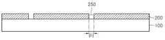
도 1을 참조하여, 기판(100) 상에 다수 개의 후면전극(200)들이 형성된다.Referring to FIG. 1, a plurality of
상기 기판(100)은 유리(glass)가 사용될 수 있으며, 세라믹 기판, 금속기판 또는 폴리머 기판 등도 사용될 수 있다.The
예를 들어, 유리 기판으로는 소다라임 유리(sodalime glass) 또는 고변형점 소다유리(high strained point soda glass)를 사용할 수 있다. 금속 기판으로는 스테인레스 스틸 또는 티타늄을 포함하는 기판을 사용할 수 있다 폴리머 기판으로는 폴리이미드(polyimide)를 사용할 수 있다.For example, soda lime glass or high strained point soda glass may be used as the glass substrate. As the metal substrate, a substrate including stainless steel or titanium may be used. As the polymer substrate, polyimide may be used.
상기 기판(100)은 투명할 수 있다. 상기 기판(100)은 리지드(rigid)하거나 플렉서블(flexible) 할 수 있다.The
상기 후면전극(200)은 상기 기판(100) 상에 후면전극층(미도시)을 형성하고, 각 셀에 대응하도록 제1 관통홀 예정영역(P1)으로 정의된 상기 후면전극층을 선택 적으로 패터닝하여 제1 관통홀(250)을 형성할 수 있다.The
즉, 상기 후면전극(200)은 제1 관통홀(250)에 의하여 서로 분리될 수 있다. 상기 제1 관통홀(250)은 상기 기판(100)의 상면을 선택적으로 노출시킬 수 이다.That is, the
예를 들어, 상기 제1 관통홀(250)은 기계적 장치 또는 레이저 장치에 의하여 형성될 수 있다. 상기 제1 관통홀(250)의 폭은 80±20㎛일 수 있다.For example, the first through
상기 후면전극(200)은 금속 등의 도전체로 형성될 수 있다.The
예를 들어, 상기 후면전극(200)은 몰리브덴(Mo)을 타겟으로 사용하여, 스퍼터링(sputtering) 공정에 의해 형성될 수 있다.For example, the
이는, 몰리브덴(Mo)이 가진 높은 전기전도도, 광 흡수층과의 오믹(ohmic) 접합, Se 분위기 하에서의 고온 안정성 때문이다.This is because of high electrical conductivity of molybdenum (Mo), ohmic bonding with the light absorbing layer, and high temperature stability under Se atmosphere.
상기 후면전극(200)인 몰리브덴(Mo) 박막은 전극으로서 비저항이 낮아야하고, 열팽창 계수의 차이로 인하여 박리현상이 일어나지 않도록 기판(100)에의 점착성이 뛰어나야 한다.The molybdenum (Mo) thin film, which is the
한편, 상기 후면전극(200)을 형성하는 물질은 이에 한정되지 않고, 나트륨(Na) 이온이 도핑된 몰리브덴(Mo)으로 형성될 수도 있다.The material forming the
도면에 도시되지는 않았지만, 상기 후면전극(200)은 적어도 하나 이상의 층으로 형성될 수 있다. 상기 후면전극(200)이 복수개의 층으로 형성될 때, 상기 후면전극(200)을 이루는 층들은 서로 다른 물질로 형성될 수 있다.Although not shown in the drawing, the
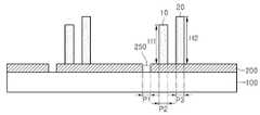
도 2를 참조하여, 상기 후면전극(200) 상에 제1 마스크 패턴(10) 및 제2 마스크 패턴(20)이 형성된다.Referring to FIG. 2, a
상기 제1 마스크 패턴(10)은 제2 관통홀 예정영역(P2)에 형성될 수 있다. 상기 제2 마스크 패턴(20)은 제3 관통홀 예정영역(P3)에 형성될 수 있다.The
예를 들어, 상기 제1 마스크 패턴(10) 및 제2 마스크 패턴(20)의 너비는 80±20㎛ 일 수 있다.For example, the widths of the
상기 제1 마스크 패턴(10)은 상기 제1 관통홀(250)과 인접하여 형성될 수 있다. 예를 들어, 상기 제1 마스크 패턴(10)은 상기 제1 관통홀(250)과 제1 갭(G1)을 가지도록 형성될 수 있다.The
상기 제2 마스크 패턴(20)은 상기 제1 마스크 패턴(10)과 인접하여 형성될 수 있다. 예를 들어, 상기 제2 마스크 패턴(20)과 상기 제1 마스크 패턴(10)은 제2 갭(G2)을 가지도록 형성될 수 있다.The
예를 들어, 상기 제1 갭(G1) 및 제2 갭(G2)의 너비는 80±20㎛ 일 수 있다.For example, the widths of the first gap G1 and the second gap G2 may be 80 ± 20 μm.
상기 제1 및 제2 마스크 패턴(20,30)은 동일한 높이 또는 서로 다른 높이를 가질 수 있다.The first and
예를 들어, 상기 제1 마스크 패턴(10)은 제1 높이(H1)로 형성되고 상기 제2 마스크 패턴(20)은 상기 제1 높이(H1) 보다 높은 제2 높이(H2)로 형성될 수도 있다. 상기 제1 마스크 패턴(10) 및 제2 마스크 패턴(20)은 1~5㎛의 높이를 가질 수 있다.For example, the
상기 제1 및 제2 마스크 패턴(20,30)은 열 경화성 또는 광 경화성 수지로 형성될 수 있다. 또는 상기 제1 및 제2 마스크 패턴(20,30)은 산화막 또는 질화막과 같은 절연성 물질로 형성될 수 있다.The first and
예를 들어, 상기 제1 및 제2 마스크 패턴(20,30)은 포토레지스트(photoresist) 물질 또는 레진(resin)과 같은 물질로 형성될 수 있다.For example, the first and
상기 제1 및 제2 마스크 패턴(20,30)의 형성은 상기 후면전극(200)을 포함하는 상기 기판(100) 상에 포토레지스트막을 스핀 코팅 등에 의하여 도포한다. 그리고, 상기 포토레지스트막 상에 제2 및 제3 관통홀 예정영역(P2,P3)을 정의하는 노광 마스크(미도시)를 위치시킨다. 그리고, 상기 노광 마스크에 의한 노광 및 현상 공정을 진행하여 상기 제1 및 제2 마스크 패턴(20,30)을 형성할 수 있다. 이때, 상기 제1 마스크 패턴(10) 및 제2 마스크 패턴(20)은 동시에 형성될 수 있다.The first and
이와는 다르게 도 3에 도시된 바와 같이, 상기 제1 마스크 패턴(10)을 포지티브 타입의 포토레지스트를 사용한 포토리소그피 공정에 의하여 형성하고, 상기 제2 마스크 패턴(20)은 네거티브 타입의 포토레지스트를 사용한 포토리소그라피 공정에 의하여 형성할 수 있다.Alternatively, as shown in FIG. 3, the
즉, 빛이나 방사선에 노출되면 그 부분만 구조변화를 일으켜, 용매에 녹지 않는 네거티브 타입, 그 반대로 쉽게 녹은 포티지브 타입의 레지스트를 각각 사용함으로써 다른 특성의 제1 마스크 패턴(10) 및 제2 마스크 패턴(20)을 형성할 수 있다.That is, when exposed to light or radiation, only a part of the structure changes, and a negative type that does not dissolve in a solvent and vice versa, which is easily melted, is used, respectively, so that the
도 4를 참조하여, 상기 제1 관통홀(250)을 포함하는 후면전극(200) 상에 광 흡수층(300)이 형성된다.Referring to FIG. 4, the
상기 광 흡수층(300)은 상기 제1 및 제2 마스크 패턴(20,30)보다 낮은 높이로 형성될 수 있다. 즉, 상기 제1 마스크 패턴(10) 및 제2 마스크 패턴(20)은 상기 광 흡수층(300) 상면에서 돌출된 형태를 가질 수 있다.The light
상기 광 흡수층(300)은 Ⅰb-Ⅲb-Ⅵb계 화합물을 포함한다.The light
더 자세하게, 상기 광 흡수층(300)은 구리-인듐-갈륨-셀레나이드계(Cu(In, Ga)Se2, CIGS계) 화합물을 포함한다.In more detail, the
이와는 다르게, 상기 광 흡수층(300)은 구리-인듐-셀레나이드계(CuInSe2, CIS계) 화합물 또는 구리-갈륨-셀레나이드계(CuGaSe2, CGS계) 화합물을 포함할 수 있다.Alternatively, the
예를 들어, 상기 광 흡수층(300)은 전해도금 공정을 통해 형성될 수 있다.For example, the
상기 광 흡수층(300) 형성시 시드막으로 몰리브덴(Mo) 또는 구리(Cu)막을 먼저 형성한 후, 전해도금 공정을 진행할 수 있다. 또는 상기 후면전극(200)이 시드막으로 사용될 수 있으므로, 상기 시드막은 형성되지 않을 수도 있다.When the
상기 전해도금공정 시 온도는 10~200℃로 유지될 수 있다.The temperature during the electroplating process may be maintained at 10 ~ 200 ℃.
상기 전해도금공정은 MeTal-Cl, Se-Oxide 및 DI를 솔루션(solution)으로 사용하거나, 또는 MeTal-Cl, SeCl 및 Dl을 솔루션으로 사용하여 진행될 수 있다. 상기 솔루션의 pH는 1~5 일 수 있다.The electroplating process may be performed using MeTal-Cl, Se-Oxide and DI as a solution, or using MeTal-Cl, SeCl and Dl as a solution. The pH of the solution may be 1-5.
상기 전해도금공정시 사용되는 메탈(Metal)은 구리(Cu), 인듐(In), 갈륨(Ga)과 같은 Ⅰ족 및 Ⅲ족 원소일 수 있다.Metal used in the electroplating process may be a group I and group element such as copper (Cu), indium (In), gallium (Ga).
상기 전해도금공정에 의하여 상기 광 흡수층(300)은 상기 제1 관통홀(250)을 포함하는 상기 후면전극(200) 상에 균일하게 높은 밀도로 증착될 수 있다. 특히, 상기 광 흡수층(300)은 상기 제1 마스크 패턴(10) 및 제2 마스크 패턴(20) 사이 영역인 제1 갭(G1) 및 제2 갭(G2)에도 보이드 없이 증착될 수 있다.By the electroplating process, the
상기 광 흡수층(300)은 상기 제1 마스크 패턴(10) 및 제2 마스크 패턴(20)을 제외한 상기 후면전극(200) 상에 형성된다.The light
이때, 상기 제1 및 제2 마스크 패턴(20,30)과 상기 후면전극(200)이 접속하는 영역을 제외한 나머지 영역에 해당하는 상기 후면전극(200)의 표면을 따라 MoSe2로 형성된 합금막(400)이 형성될 수 있다.In this case, an alloy film formed of MoSe2 along the surface of the
즉, 상기 광 흡수층(300)의 형성시 상기 몰리브덴 막박과 셀레늄이 화학적 결합을 하여 상기 후면전극(200)의 표면에는 MoSe2층이 형성될 수 있다. 이때, 상기 제2 및 제3 관통홀 예정영역(P2,P3)에 해당하는 상기 후면전극(200)의 표면에는 상기 제1 및 제2 마스크 패턴(20,30)이 형성되어 있으므로 MoSe2 합금막(400)이 형성되지 않게 된다.That is, when the
상기 광 흡수층(300)이 저온공정인 전해도금공정을 통해 형성되므로, 실시예에서는 플렉서블한 기판(100)의 적용이 가능할 수 있다.Since the
상기 광 흡수층(300)은 외부의 광을 입사받아, 전기 에너지로 변환시킨다. 상기 광 흡수층(300)은 광전효과에 의해서 광 기전력을 생성한다.The light
일반적으로 단위 셀의 전면전극과 후면전극을 연결하기 위해서 광 흡수층을 관통하도록 스크라이빙 공정을 통해 관통홀을 형성한다. 또한, 단위 셀을 분리하기 위한 패터닝 역시 스크라이빙 공정을 통해 형성한다. 하지만, 이러한 스크라이빙 공정에 의한 관통홀의 패턴은 불균일하게 형성되어 데드존 영역을 증가시킬 수 있다. 또한 상기 후면전극(200)과 광 흡수층(300)의 계면에 형성된 MoSe2의 제거가 용이하지 않으므로, 콘택 저항이 증가되는 문제가 있었다.In general, a through hole is formed through a scribing process to penetrate the light absorbing layer to connect the front electrode and the rear electrode of the unit cell. In addition, patterning for separating the unit cells is also formed through a scribing process. However, the pattern of the through hole by this scribing process may be formed non-uniformly to increase the dead zone area. In addition, since the removal of MoSe2 formed at the interface between the
실시예에서는 제2 및 제3 관통홀 예정영역(P2,P3)에 상기 제1 및 제2 마스크 패턴(20,30)을 상기 후면전극(200) 상에 먼저 형성한 후 광 흡수층(300)이 형성되므로 별도의 스크라이빙 공정이 생략될 수 있다. 또한, 상기 제2 및 제3 관통홀 예정영역(P2,P3)에 MoSe2가 형성되지 않으므로 전면전극과 후면전극(200)의 콘택특성을 향상시킬 수 있다.In an embodiment, the first and
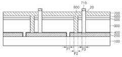
도 5를 참조하여, 상기 광 흡수층(300) 상에 버퍼층(500) 및 고저항 버퍼층(600)이 형성된다.Referring to FIG. 5, a
상기 버퍼층(500)은 상기 광 흡수층(300) 상에 적어도 하나 이상의 층으로 형성될 수 있으며, 황화 카드뮴(CdS)이 적층되어 형성될 수 있다.The
이때, 상기 버퍼층(500)은 n형 반도체 층이고, 상기 광 흡수층(300)은 p형 반도체 층이다. 따라서, 상기 광 흡수층(300) 및 버퍼층(500)은 pn접합을 형성한다.In this case, the
상기 고저항 버퍼층(600)은 산화 아연(ZnO)를 타겟으로 한 스퍼터링 공정을 진행하여, 상기 황화 카드뮴(CdS) 상에 산화 아연층이 더 형성될 수 있다.The high
상기 고저항 버퍼층(600)은 상기 버퍼층(500) 상에 투명전극층으로 형성될 수 있다.The high
예를 들어, 상기 고저항 버퍼층(600)은 ITO, ZnO 및 i-ZnO 중 어느 하나로 형성될 수 있다.For example, the high
상기 버퍼층(500) 및 고저항 버퍼층(600)은 상기 제1 및 제2 마스크 패턴(20,30)보다 낮은 높이로 형성될 수 있다. 즉, 상기 제1 마스크 패턴(10) 및 제2 마스크 패턴(20)은 상기 버퍼층(500) 상면에서 돌출된 형태를 가질 수 있다.The
또는 상기 고저항 버퍼층(600)은 상기 제1 마스크 패턴(10)과 동일한 높이로 형성되고, 상기 제1 마스크 패턴(10)의 상면은 상기 고저항 버퍼층(600) 상부로 노출될 있다.Alternatively, the high
상기 버퍼층(500) 및 고저항 버퍼층(600)은 상기 광 흡수층(300)과 이후 형성된 전면전극의 사이에 배치된다.The
즉, 상기 광 흡수층(300)과 전면전극층은 격자상수와 에너지 밴드 갭의 차이가 크기 때문에, 밴드 갭이 두 물질의 중간에 위치하는 상기 버퍼층(500) 및 고저항 버퍼층을 삽입하여 양호한 접합을 형성할 수 있다.That is, since the difference between the lattice constant and the energy band gap is large between the light absorbing
본 실시예에서는 두 개의 버퍼층(500)을 상기 광 흡수층(300) 상에 형성하였지만, 이에 한정되지 않고, 상기 버퍼층(500)은 한개의 층으로만 형성될 수 있다.In the present exemplary embodiment, two
도 6을 참조하여, 상기 제1 마스크 패턴(10)을 제거하고 제2 관통홀(650)이 형성된다.Referring to FIG. 6, the
상기 제1 마스크 패턴(10)은 상기 고저항 버퍼층(600), 버퍼층(500) 및 광 흡수층(300)을 관통하여 상기 후면전극(200) 상에 형성된 상태이므로, 상기 제1 마스크 패턴(10)의 선택적 제거에 의하여 상기 제2 관통홀(650)이 형성될 수 있다.Since the
상기 제2 관통홀(650)은 상기 후면전극(200)을 선택적으로 노출시킬 수 있다. 상기 제2 관통홀(650)은 상기 제1 관통홀(250)과 제1 갭(G1)을 가지도록 형성될 수 있다.The second through
상기 제1 마스크 패턴(10)에 상기 후면전극(200)의 표면에는 MoSe2가 형성되지 않았기 때문에, 상기 제2 관통홀(650)은 상기 후면전극(200)의 상부 표면을 직접 노출시킬 수 있다.Since MoSe2 is not formed on the surface of the
도 7을 참조하여, 상기 제2 관통홀(650)을 포함하는 상기 고저항 버퍼층(600) 상에 투명한 도전물질을 적층하여 전면전극층(700)이 형성된다.Referring to FIG. 7, the
상기 전면전극층(700)이 형성될 때, 상기 투명한 도전물질이 상기 제2 관통홀(650)에도 삽입되어 접속배선(800)을 형성할 수 있다.When the
상기 전면전극층(700)은 스퍼터링 공정을 진행하여 알루미늄(Al) 또는 알루미나(Al2O3)로 도핑된 산화 아연으로 형성된다.The
예를 들어, 상기 전면전극층(700)은 800nm±100의 두께로 형성될 수 있다.For example, the
상기 전면전극층(700)은 상기 광 흡수층(300)과 pn접합을 형성하는 윈도우(window)층으로서, 태양전지 전면의 투명전극의 기능을 하기 때문에 광투과율이 높고 전기 전도성이 좋은 산화 아연(ZnO)으로 형성된다.The
따라서, 상기 산화 아연에 알루미늄 또는 알루미나를 도핑함으로써 낮은 저항값을 갖는 전극을 형성할 수 있다.Therefore, it is possible to form an electrode having a low resistance value by doping aluminum or alumina to the zinc oxide.
상기 전면전극층(700)인 산화 아연 박막은 RF 스퍼터링방법으로 ZnO 타겟을 사용하여 증착하는 방법과 Zn 타겟을 이용한 반응성 스퍼터링, 그리고 유기금속화학증착법 등으로 형성될 수 있다.The zinc oxide thin film as the
또한, 전기광학적 특성이 뛰어난 ITO(Indium Thin Oxide) 박막을 산화 아연 박막 상에 층착한 2중 구조를 형성할 수도 있다.In addition, a double structure in which an indium thin oxide (ITO) thin film having excellent electro-optic properties is laminated on a zinc oxide thin film may be formed.
상기 전면전극층(700)은 상기 제2 마스크 패턴(20)보다 낮은 높이로 형성될 수 있다. 즉, 상기 제2 마스크 패턴(20)은 상기 전면전극층(700) 상면에서 돌출된 형태를 가질 수 있다.The
상기 접속배선(800)에 의해 각각의 셀은 서로 연결될 수 있다. 즉, 상기 접속배선(800)은 상호 인접하는 셀의 후면전극(200)과 전면전극층(700)을 물리적, 전기적으로 연결할 수 있다.Each cell may be connected to each other by the
특히, 상기 접속배선(800)은 상기 제2 관통홀(650)을 통해 상기 후면전극(200)과 직접 접촉할 수 있다. 이에 따라, 상기 접속배선(800)과 상기 후면전극(200)의 콘택특성을 향상시킬 수 있다.In particular, the
상기 제3 관통홀 예정영역(P3)에는 상기 제3 마스크 패턴(20)이 형성되어 있으므로 셀들은 각각 분리된 상태가 될 수 있다.Since the
한편, 상기 전면전극층(700)을 형성할 때 상기 제2 마스크 패턴(20)의 표면에도 상기 투명전극물질(710)이 남아있을 수도 있다.Meanwhile, when forming the
따라서, 도 8에 도시된 바와 같이, 상기 제2 마스크 패턴(20) 표면의 투명전극물질(710)을 플라즈마를 이용한 건식식각 공정을 통해 선택적으로 제거할 수 있다.Therefore, as illustrated in FIG. 8, the
추가적으로, 도 9에 도시된 바와 같이, 상기 제2 마스크 패턴(20)을 제거하고 제3 관통홀(750)을 노출시킬 수도 있다.In addition, as shown in FIG. 9, the
상기 제2 마스크 패턴(20)은 투명한 물질로 형성되어 있으므로 제거되지 않을 수도 있다.Since the
상기와 같이 제2 및 제3 관통홀에 해당하는 상기 후면전극 상에는 MoSe2가 형성되지 않으므로, 상기 후면전극과 전면전극의 컨택특성을 향상시킬 수 있다.As described above, since MoSe2 is not formed on the rear electrodes corresponding to the second and third through holes, contact characteristics between the rear electrodes and the front electrodes may be improved.
또한, 상기 광 흡수층은 저온에서 진행되는 전해도금공정을 통해 형성되므로, 실시예는 낮은 경도 또는 플렉서블한 기판의 사용이 가능하다. 이에 따라, 태양전지를 경량화시킬 수 있다.In addition, since the light absorbing layer is formed through the electroplating process proceeds at a low temperature, the embodiment can use a low hardness or a flexible substrate. As a result, the solar cell can be reduced in weight.
또한, 상기 제2 및 제3 마스크 패턴에 의하여 제2 관통홀 및 제3 관통홀이 형성되므로, 별도의 스크라이빙 공정이 생략될 수 있다.In addition, since the second through hole and the third through hole are formed by the second and third mask patterns, a separate scribing process may be omitted.
특히 스크라이빙 공정에 의한 패턴 불균일을 방지할 수 있으므로, 태양전지의 전기적 특성을 향상시킬 수 있다.In particular, since the pattern nonuniformity caused by the scribing process can be prevented, the electrical characteristics of the solar cell can be improved.
이상에서 실시예를 중심으로 설명하였으나 이는 단지 예시일 뿐 본 발명을 한정하는 것이 아니며, 본 발명이 속하는 분야의 통상의 지식을 가진 자라면 본 실시예의 본질적인 특성을 벗어나지 않는 범위에서 이상에 예시되지 않은 여러 가지의 변형과 응용이 가능함을 알 수 있을 것이다. 예를 들어, 실시예에 구체적으로 나타난 각 구성 요소는 변형하여 실시할 수 있는 것이다. 그리고 이러한 변형과 응용에 관계된 차이점들은 첨부된 청구 범위에서 규정하는 본 발명의 범위에 포함되는 것으로 해석되어야 할 것이다.Although described above with reference to the embodiment is only an example and is not intended to limit the invention, those of ordinary skill in the art to which the present invention does not exemplify the above within the scope not departing from the essential characteristics of this embodiment It will be appreciated that many variations and applications are possible. For example, each component specifically shown in the embodiment can be modified. And differences relating to such modifications and applications will have to be construed as being included in the scope of the invention defined in the appended claims.
도 1 내지 도 9는 실시예에 따른 태양전지의 제조방법을 나타내는 단면도이다.1 to 9 are cross-sectional views showing a method of manufacturing a solar cell according to the embodiment.
Claims (10)
Translated fromKoreanPriority Applications (1)
| Application Number | Priority Date | Filing Date | Title |
|---|---|---|---|
| KR1020090104466AKR101091379B1 (en) | 2009-10-30 | 2009-10-30 | Solar cell and manufacturing method thereof |
Applications Claiming Priority (1)
| Application Number | Priority Date | Filing Date | Title |
|---|---|---|---|
| KR1020090104466AKR101091379B1 (en) | 2009-10-30 | 2009-10-30 | Solar cell and manufacturing method thereof |
Publications (2)
| Publication Number | Publication Date |
|---|---|
| KR20110047724A KR20110047724A (en) | 2011-05-09 |
| KR101091379B1true KR101091379B1 (en) | 2011-12-07 |
Family
ID=44238980
Family Applications (1)
| Application Number | Title | Priority Date | Filing Date |
|---|---|---|---|
| KR1020090104466AExpired - Fee RelatedKR101091379B1 (en) | 2009-10-30 | 2009-10-30 | Solar cell and manufacturing method thereof |
Country Status (1)
| Country | Link |
|---|---|
| KR (1) | KR101091379B1 (en) |
Families Citing this family (5)
| Publication number | Priority date | Publication date | Assignee | Title |
|---|---|---|---|---|
| KR101222559B1 (en)* | 2010-12-27 | 2013-01-16 | 주식회사 아바코 | Solar cell and method of manufacturing the same |
| KR101277109B1 (en)* | 2010-12-27 | 2013-06-20 | 주식회사 아바코 | Method of manufacturing a solar cell |
| KR101166456B1 (en)* | 2011-05-23 | 2012-07-19 | 김병국 | Solar cell and method for fabricating the same |
| CN104091854B (en)* | 2013-04-01 | 2017-06-20 | 北京恒基伟业投资发展有限公司 | The production method and its electric deposition device of a kind of thin-film solar cells |
| CN105206703B (en)* | 2014-05-26 | 2018-04-27 | 北京恒基伟业投资发展有限公司 | The production method and its electric deposition device of a kind of thin-film solar cells |
- 2009
- 2009-10-30KRKR1020090104466Apatent/KR101091379B1/ennot_activeExpired - Fee Related
Also Published As
| Publication number | Publication date |
|---|---|
| KR20110047724A (en) | 2011-05-09 |
Similar Documents
| Publication | Publication Date | Title |
|---|---|---|
| KR101173344B1 (en) | Solar cell and mehtod of fabricating the same | |
| KR101144570B1 (en) | Solar cell and method of fabircating the same | |
| KR101154763B1 (en) | Solar cell and method of fabricating the same | |
| US8779282B2 (en) | Solar cell apparatus and method for manufacturing the same | |
| KR101262455B1 (en) | Solar cell apparatus and method of fabricating the same | |
| KR101091475B1 (en) | Solar cell and manufacturing method thereof | |
| KR101091379B1 (en) | Solar cell and manufacturing method thereof | |
| KR101114099B1 (en) | Solar cell apparatus and method of fabricating the same | |
| KR101114018B1 (en) | Solar cell and method of fabricating the same | |
| KR101241467B1 (en) | Solar cell and preparing method of the same | |
| KR101189309B1 (en) | Solar cell and solar cell module | |
| JP5602234B2 (en) | Photovoltaic power generation apparatus and manufacturing method thereof | |
| KR101091359B1 (en) | Solar cell and manufacturing method thereof | |
| KR101272997B1 (en) | Solar cell apparatus and method of fabricating the same | |
| KR20110035733A (en) | Solar cell and manufacturing method thereof | |
| KR101028310B1 (en) | Solar cell and manufacturing method thereof | |
| KR101172178B1 (en) | Solar cell apparatus and method of fabricating the same | |
| KR101144447B1 (en) | Solar cell apparatus and method of fabricating the same | |
| KR20120086447A (en) | Solar cell apparatus and method of fabricating the same | |
| KR101306525B1 (en) | Solar cell module and method of fabricating the same | |
| CN103069577B (en) | Solar cell and manufacture method thereof | |
| KR101072170B1 (en) | Solar cell and method of fabricating the same | |
| KR20110041248A (en) | Solar cell and manufacturing method thereof | |
| KR101091499B1 (en) | Tip, the solar cell and method of fabricating the solar cell using the tip | |
| KR101543034B1 (en) | Tip and manufacturing method of solar cell using the same |
Legal Events
| Date | Code | Title | Description |
|---|---|---|---|
| A201 | Request for examination | ||
| PA0109 | Patent application | St.27 status event code:A-0-1-A10-A12-nap-PA0109 | |
| PA0201 | Request for examination | St.27 status event code:A-1-2-D10-D11-exm-PA0201 | |
| R18-X000 | Changes to party contact information recorded | St.27 status event code:A-3-3-R10-R18-oth-X000 | |
| E902 | Notification of reason for refusal | ||
| PE0902 | Notice of grounds for rejection | St.27 status event code:A-1-2-D10-D21-exm-PE0902 | |
| P11-X000 | Amendment of application requested | St.27 status event code:A-2-2-P10-P11-nap-X000 | |
| P13-X000 | Application amended | St.27 status event code:A-2-2-P10-P13-nap-X000 | |
| PG1501 | Laying open of application | St.27 status event code:A-1-1-Q10-Q12-nap-PG1501 | |
| E701 | Decision to grant or registration of patent right | ||
| PE0701 | Decision of registration | St.27 status event code:A-1-2-D10-D22-exm-PE0701 | |
| GRNT | Written decision to grant | ||
| PR0701 | Registration of establishment | St.27 status event code:A-2-4-F10-F11-exm-PR0701 | |
| PR1002 | Payment of registration fee | St.27 status event code:A-2-2-U10-U11-oth-PR1002 Fee payment year number:1 | |
| PG1601 | Publication of registration | St.27 status event code:A-4-4-Q10-Q13-nap-PG1601 | |
| P22-X000 | Classification modified | St.27 status event code:A-4-4-P10-P22-nap-X000 | |
| PN2301 | Change of applicant | St.27 status event code:A-5-5-R10-R13-asn-PN2301 St.27 status event code:A-5-5-R10-R11-asn-PN2301 | |
| FPAY | Annual fee payment | Payment date:20141106 Year of fee payment:4 | |
| PR1001 | Payment of annual fee | St.27 status event code:A-4-4-U10-U11-oth-PR1001 Fee payment year number:4 | |
| FPAY | Annual fee payment | Payment date:20151105 Year of fee payment:5 | |
| PR1001 | Payment of annual fee | St.27 status event code:A-4-4-U10-U11-oth-PR1001 Fee payment year number:5 | |
| FPAY | Annual fee payment | Payment date:20161104 Year of fee payment:6 | |
| PR1001 | Payment of annual fee | St.27 status event code:A-4-4-U10-U11-oth-PR1001 Fee payment year number:6 | |
| R18-X000 | Changes to party contact information recorded | St.27 status event code:A-5-5-R10-R18-oth-X000 | |
| FPAY | Annual fee payment | Payment date:20171107 Year of fee payment:7 | |
| PR1001 | Payment of annual fee | St.27 status event code:A-4-4-U10-U11-oth-PR1001 Fee payment year number:7 | |
| P22-X000 | Classification modified | St.27 status event code:A-4-4-P10-P22-nap-X000 | |
| R18-X000 | Changes to party contact information recorded | St.27 status event code:A-5-5-R10-R18-oth-X000 | |
| LAPS | Lapse due to unpaid annual fee | ||
| PC1903 | Unpaid annual fee | St.27 status event code:A-4-4-U10-U13-oth-PC1903 Not in force date:20181202 Payment event data comment text:Termination Category : DEFAULT_OF_REGISTRATION_FEE | |
| PC1903 | Unpaid annual fee | St.27 status event code:N-4-6-H10-H13-oth-PC1903 Ip right cessation event data comment text:Termination Category : DEFAULT_OF_REGISTRATION_FEE Not in force date:20181202 | |
| R18-X000 | Changes to party contact information recorded | St.27 status event code:A-5-5-R10-R18-oth-X000 | |
| PN2301 | Change of applicant | St.27 status event code:A-5-5-R10-R13-asn-PN2301 St.27 status event code:A-5-5-R10-R11-asn-PN2301 | |
| P22-X000 | Classification modified | St.27 status event code:A-4-4-P10-P22-nap-X000 |