KR101091023B1 - Memory Cell String Stacks and Memory Arrays Using the Same - Google Patents
Memory Cell String Stacks and Memory Arrays Using the SameDownload PDFInfo
- Publication number
- KR101091023B1 KR101091023B1KR1020100099171AKR20100099171AKR101091023B1KR 101091023 B1KR101091023 B1KR 101091023B1KR 1020100099171 AKR1020100099171 AKR 1020100099171AKR 20100099171 AKR20100099171 AKR 20100099171AKR 101091023 B1KR101091023 B1KR 101091023B1
- Authority
- KR
- South Korea
- Prior art keywords
- semiconductor
- lines
- stacks
- layer
- insulating film
- Prior art date
- Legal status (The legal status is an assumption and is not a legal conclusion. Google has not performed a legal analysis and makes no representation as to the accuracy of the status listed.)
- Active
Links
Images


Classifications
- H—ELECTRICITY
- H10—SEMICONDUCTOR DEVICES; ELECTRIC SOLID-STATE DEVICES NOT OTHERWISE PROVIDED FOR
- H10B—ELECTRONIC MEMORY DEVICES
- H10B63/00—Resistance change memory devices, e.g. resistive RAM [ReRAM] devices
- H10B63/80—Arrangements comprising multiple bistable or multi-stable switching components of the same type on a plane parallel to the substrate, e.g. cross-point arrays
- H—ELECTRICITY
- H10—SEMICONDUCTOR DEVICES; ELECTRIC SOLID-STATE DEVICES NOT OTHERWISE PROVIDED FOR
- H10B—ELECTRONIC MEMORY DEVICES
- H10B63/00—Resistance change memory devices, e.g. resistive RAM [ReRAM] devices
- H10B63/30—Resistance change memory devices, e.g. resistive RAM [ReRAM] devices comprising selection components having three or more electrodes, e.g. transistors
- H—ELECTRICITY
- H10—SEMICONDUCTOR DEVICES; ELECTRIC SOLID-STATE DEVICES NOT OTHERWISE PROVIDED FOR
- H10D—INORGANIC ELECTRIC SEMICONDUCTOR DEVICES
- H10D64/00—Electrodes of devices having potential barriers
- H10D64/01—Manufacture or treatment
- H10D64/031—Manufacture or treatment of data-storage electrodes
- H10D64/035—Manufacture or treatment of data-storage electrodes comprising conductor-insulator-conductor-insulator-semiconductor structures
- H—ELECTRICITY
- H10—SEMICONDUCTOR DEVICES; ELECTRIC SOLID-STATE DEVICES NOT OTHERWISE PROVIDED FOR
- H10D—INORGANIC ELECTRIC SEMICONDUCTOR DEVICES
- H10D84/00—Integrated devices formed in or on semiconductor substrates that comprise only semiconducting layers, e.g. on Si wafers or on GaAs-on-Si wafers
- H10D84/01—Manufacture or treatment
- H10D84/0123—Integrating together multiple components covered by H10D12/00 or H10D30/00, e.g. integrating multiple IGBTs
- H10D84/0126—Integrating together multiple components covered by H10D12/00 or H10D30/00, e.g. integrating multiple IGBTs the components including insulated gates, e.g. IGFETs
- H10D84/0149—Manufacturing their interconnections or electrodes, e.g. source or drain electrodes
- H—ELECTRICITY
- H10—SEMICONDUCTOR DEVICES; ELECTRIC SOLID-STATE DEVICES NOT OTHERWISE PROVIDED FOR
- H10D—INORGANIC ELECTRIC SEMICONDUCTOR DEVICES
- H10D84/00—Integrated devices formed in or on semiconductor substrates that comprise only semiconducting layers, e.g. on Si wafers or on GaAs-on-Si wafers
- H10D84/01—Manufacture or treatment
- H10D84/02—Manufacture or treatment characterised by using material-based technologies
- H10D84/03—Manufacture or treatment characterised by using material-based technologies using Group IV technology, e.g. silicon technology or silicon-carbide [SiC] technology
- H10D84/038—Manufacture or treatment characterised by using material-based technologies using Group IV technology, e.g. silicon technology or silicon-carbide [SiC] technology using silicon technology, e.g. SiGe
Landscapes
- Non-Volatile Memory (AREA)
- Semiconductor Memories (AREA)
Abstract
Description
Translated fromKorean본 발명은 비휘발성 메모리에 관한 것으로, 더욱 상세하게는 수직으로 적층된 메모리 셀 스트링 스택 및 이를 이용한 메모리 어레이에 관한 것이다.The present invention relates to a nonvolatile memory, and more particularly, to a memory cell string stack and a memory array using the same stacked vertically.
최근 비휘발성 메모리는 가전 및 휴대용 전자기기에서 그 수요가 급속히 증가하고 있어 지속적인 성장이 가능할 것으로 예상되고 있다.Recently, the demand for nonvolatile memory is rapidly increasing in home appliances and portable electronic devices.
특히 낸드(NAND) 비휘발성 메모리의 집적도는 IT 기술의 발전에 따라 계속 증가되는 것이 요구되고 있다. 낸드 비휘발성 메모리의 집적도는 셀 소자의 집적도에 의해 크게 좌우된다. 최근, 셀 소자의 게이트 길이가 50 nm 이하로 줄어들고 있고, 메모리 용량은 수십 기가 비트에 이르고 있다. 따라서 기존의 도전성 플로팅 게이트를 갖는 평탄 채널 구조의 비휘발성 메모리 소자는 짧은채널효과가 큰 문제로 대두되어 있고, 제조 공정도 크게 어려워지는 문제에 직면했다. 게이트 길이가 50 nm 이하인 기술은 고가의 장비나 공정을 필요로 하므로 제조 단가가 증가하는 문제점이 있다. 향후 계속해서 게이트 길이가 줄어들어야 집적도를 향상시킬 수 있는데, 이러한 상황에 대처할 수 있는 대안이 요구되고 있다.In particular, the density of NAND nonvolatile memory is required to increase continuously with the development of IT technology. The degree of integration of the NAND nonvolatile memory is highly dependent on the degree of integration of the cell devices. In recent years, gate lengths of cell devices have been reduced to 50 nm or less, and memory capacities have reached tens of gigabytes. Therefore, the conventional non-volatile memory device having a flat floating channel structure having a conductive floating gate is a problem that the short channel effect is a big problem, and the manufacturing process is also very difficult. The technology having a gate length of 50 nm or less requires expensive equipment or processes and thus increases manufacturing costs. In the future, the gate length must be reduced to improve the density, and there is a need for an alternative to cope with this situation.
메모리 셀 소자의 집적도를 높이기 위하여 기존의 플로팅 게이트를 갖는 메모리 셀 대신 질화막과 같은 절연성 저장노드를 사용하는 SONOS 계열의 플래시 메모리 셀이 고려되고 있다. 또한, 나노 dot 또는 나노 crystal을 전하 저장노드로 사용하는 NFGM(Nano-Floating Gate Memory) 셀이 고려되고 있다. 기존의 평탄 채널 구조에 질화막이나 나노 dot과 같은 전하 저장노드를 사용하여 메모리 셀을 구현할 경우, 기존의 도전성 폴리 실리콘의 플로팅 게이트를 사용한 경우에 비해 축소화 특성이 개선된다. 그러나 이러한 개선된 전하 저장노드를 사용하더라도 40 nm 급 또는 그 이하의 게이트 길이에 대해서는 짧은채널효과에 의해 특성이 크게 저하되어 축소화가 불가능한 한계에 직면하게 된다.In order to increase the density of memory cell devices, a SONOS-based flash memory cell using an insulating storage node such as a nitride film instead of a memory cell having a floating gate has been considered. In addition, nano-floating gate memory (NFGM) cells using nano dots or nano crystals as charge storage nodes have been considered. When a memory cell is implemented by using a charge storage node such as a nitride film or a nano dot in a conventional flat channel structure, the miniaturization characteristic is improved as compared with the case of using a floating gate of conductive polysilicon. However, even when the improved charge storage node is used, the characteristics of the gate length of 40 nm or less are greatly reduced due to the short channel effect, and thus the limit of the reduction is impossible.
셀 소자의 게이트 길이를 40 nm 또는 그 이하로 줄일 경우 발생하는 짧은채널효과를 억제하고 문턱전압의 산포를 줄이기 위해 평탄 채널 구조에서 비대칭 소스/드레인 구조를 갖는 SONOS 혹은 TANOS(TaN-AlO-SiN-Oxide-Si) 셀 소자(K. T. Park et al., A 64-cell NAND flash memory with asymmetric S/D structure for sub-40 nm technology and beyond, in Technical Digest of Symposium on VLSI Technology, p. 24, 2006)가 삼성전자에 의해 발표되었다. 셀 소자의 게이트를 중심으로 한쪽은 소스/드레인에 해당하는 불순물 도핑 영역이 있으나, 다른 쪽에는 소스/드레인을 위한 불순물 도핑 영역이 없는 구조이다. 이는 불순물 도핑 대신 이웃 제어전극으로부터의 프린징(fringing) 전계로 형성되는 반전층(inversion layer)으로 가상 소스/드레인을 형성하도록 함으로써 짧은채널효과를 억제하는 구조이다. 비록 기존의 불순물 도핑으로 양측 소스/드레인을 형성하는 평탄 채널을 갖는 SONOS 셀 소자에 비해 축소화 특성은 개선되지만, 셀 소자의 양측 소스/드레인 중 어느 한쪽은 제어전극과 겹치는 형태로 형성되기 때문에 40 nm 이하의 채널 길이에서 여전히 짧은채널효과를 보이며, 궁극적으로 평탄 채널 구조가 갖는 축소화 한계에 직면하게 된다.SONOS or TANOS (TaN-AlO-SiN-) with an asymmetric source / drain structure in a flat channel structure to suppress short channel effects and reduce threshold voltages caused by reducing the gate length of the cell device to 40 nm or less. Oxide-Si) Cell Device (KT Park et al., A 64-cell NAND flash memory with asymmetric S / D structure for sub-40 nm technology and beyond, in Technical Digest of Symposium on VLSI Technology, p. 24, 2006) Was announced by Samsung Electronics. The impurity doped region corresponding to the source / drain is formed on one side of the gate of the cell device, but the impurity doped region for the source / drain is not formed on the other side. This structure suppresses short channel effects by forming a virtual source / drain into an inversion layer formed by fringing electric fields from neighboring control electrodes instead of impurity doping. Although the reduction characteristics are improved compared to SONOS cell devices having flat channels that form both sources / drains by conventional impurity doping, one of the two sources / drains of the cell devices is formed to overlap the control electrode. Short channel effects are still seen at the following channel lengths and ultimately face the miniaturization limitation of flat channel structures.
제조 단가를 줄이면서 집적도를 높일 수 있는 방법은 셀 소자나 셀 스트링을 수직으로 형성하는 방법이 있다. 미국 특허(등록번호: 5739567, 명칭: Highly compact memory device with nonvolatile vertical transistor memory cell)에서는 트렌치를 형성하고 터널링 절연막, 플로팅 게이트, 블로킹 절연막 및 제어전극을 트렌치 내에 순차적으로 형성하여 구현하였다. 소스는 트렌치의 바닥 근처 반도체 영역에, 그리고 드레인은 트렌치의 상부 근처 반도체 영역에 각각 형성하였다. 이 구조에서는 수직형 셀 소자가 1개만 형성되어 실질적으로 메모리 용량을 높일 수 없으며, 구조적인 문제로 인해 여러 개의 셀 소자들을 수직으로 형성할 수 없다.One way to increase the degree of integration while reducing manufacturing costs is to form cell elements or cell strings vertically. In the US patent (Registration No. 5739567, namely: Highly compact memory device with nonvolatile vertical transistor memory cell), a trench is formed, and a tunneling insulating film, a floating gate, a blocking insulating film, and a control electrode are sequentially formed in the trench. Sources were formed in the semiconductor region near the bottom of the trench, and drains in the semiconductor region near the top of the trench, respectively. In this structure, only one vertical cell element is formed to substantially increase the memory capacity, and due to structural problems, it is impossible to form multiple cell elements vertically.
최근 발표된 논문(Y. Fukuzumi et al., Optimal integration and characteristics of vertical array devices for ultra-high density, bit-cost scalable flash memory, IEDM Tech. Dig., pp. 449-452, 2007)에서는 상기 미국 특허가 갖는 문제점을 해결하기 위해 수직으로 여러 개의 셀들과 두 개의 스위치 소자들을 배치하고 있다. 이에 의하면, 집적도는 높일 수 있으나, 쓰기 시간이 다소 느리고, 특히 지우기 시간이 느린 단점이 있다. 또한, 유지시간(retention) 특성이 나쁘다. 제조공정에 있어서 수직으로 적층되는 여러 층의 제어전극들 사이에 전기적 절연을 위해 절연층을 형성한다. 이 경우 하나의 스트링을 형성하기 위해 원 모양의 비아홀(via hole)을 형성할 때, 폴리실리콘으로 구성되는 제어전극과 실리콘 산화막으로 구성되는 절연층을 번갈아 가면서 계속 식각해야 하는데, 이는 공정적으로 매우 어렵고 많은 시간을 소요할 수 있다. 또한 튜브(tube) 형태의 바디를 수직으로 형성할 때 바닥이 반도체 영역과 전기적으로 연결되도록 하기 위해서 비아홀의 수직 측벽에 형성된 게이트 절연막 또는 블로킹 절연막은 남기고 비아홀 바닥에 있는 것만 식각해야 한다. 이때 측벽의 절연막이 손상을 입을 수 있고, 이는 메모리 셀 특성의 저하로, 결국 수율이 저하될 수 있다. 비아홀의 바닥에 형성되는 소스 영역을 비아홀의 상부 표면으로부터 전기적인 컨택을 하고 배선을 하려면 큰 단차를 극복해야 함은 물론이고 추가의 마스크를 필요로 할 수 있다. 요컨대 공정적 측면에서 많은 어려움이 있다.In a recent paper (Y. Fukuzumi et al., Optimal integration and characteristics of vertical array devices for ultra-high density, bit-cost scalable flash memory, IEDM Tech. Dig., Pp. 449-452, 2007) In order to solve the problem of the patent, several cells and two switch elements are arranged vertically. According to this, although the degree of integration can be increased, the write time is rather slow, and in particular, the erase time is slow. In addition, the retention characteristics are poor. In the manufacturing process, an insulating layer is formed for electrical insulation between control layers of various layers stacked vertically. In this case, when forming a via via of a circle to form a string, it is necessary to continue to etch alternately between the control electrode made of polysilicon and the insulating layer made of silicon oxide. It can be difficult and time consuming. In addition, in order to form a tube-shaped body vertically, only the bottom of the via hole may be etched, leaving a gate insulating film or a blocking insulating film formed on the vertical sidewall of the via hole so that the bottom is electrically connected to the semiconductor region. At this time, the insulating film on the sidewall may be damaged, which may result in deterioration of the memory cell characteristics and, in turn, lower the yield. The electrical contact and wiring of the source region formed at the bottom of the via hole from the upper surface of the via hole may require a large mask as well as overcoming a large step. In short, there are many difficulties in terms of fairness.
상기와 같은 기존의 발표된 소자들이 갖는 문제점을 해결할 수 있는 새로운 구조의 고집적/고성능 비휘발성 메모리 소자를 개발할 필요성이 요구되었다.There is a need for developing a highly integrated / high performance nonvolatile memory device having a new structure that can solve the problems of the existing published devices.
본 발명은 상기 종래기술의 문제점을 해결하고자, 수평의 제 1 방향으로 복수개의 메모리 셀 소자들이 형성되는 셀 스트링을 절연층을 사이에 두고 수직으로 적층시킬 때, 상하 형성되는 셀 소자 간의 전하 저장노드가 서로 연결되지 않게 함으로써, 상하 셀 소자 간의 전하 이동을 원천 차단할 수 있는 메모리 셀 스트링 스택을 제공함을 그 목적으로 한다.In order to solve the problems of the prior art, a charge storage node between upper and lower cell elements formed when vertically stacking a cell string in which a plurality of memory cell elements are formed in a horizontal first direction with an insulating layer interposed therebetween. It is an object of the present invention to provide a memory cell string stack capable of blocking the transfer of charge between upper and lower cell elements by preventing them from being connected to each other.
또한, 수직으로 적층된 메모리 셀 스트링 스택이 수평의 제 2 방향으로 복수개 형성되며, 각 셀 소자를 구동할 수 있도록 배선이 형성된 메모리 어레이를 제공함을 다른 목적으로 한다.It is another object of the present invention to provide a memory array in which a plurality of vertically stacked memory cell string stacks are formed in a second horizontal direction and in which wirings are formed to drive respective cell elements.
상기 목적을 달성하기 위하여, 본 발명에 의한 메모리 어레이는 반도체 기판 상에 각각 절연막과 반도체층이 교대로 반복 적층되며 수평의 제 1 방향으로 일정 길이를 갖고, 수평의 제 2 방향으로 일정 거리 이격되며 복수개 형성된 반도체 스택들; 상기 각 반도체 스택의 적어도 일 측면 상에 상기 제 1 방향을 따라 일정 거리 이격되며 복수개 형성된 전하 저장층을 포함한 게이트 절연막 스택들; 상기 각 게이트 절연막 스택 상에 상기 반도체 스택들 사이의 이격 공간에 형성된 복수개의 제어전극들; 및 상기 제어전극들 사이 및 상기 게이트 절연막 스택들 사이에 채워진 분리절연막을 포함하여 구성되되, 상기 각 반도체 스택의 각 반도체층은 일단에 상기 제 1 방향으로 일정 거리 이격되며 상기 제 2 방향으로 형성된 복수개의 비트라인들 중 어느 하나와 전기적으로 연결되고, 타단에 선택 트랜지스터를 통하여 접지되고, 상기 제어전극들은 상기 비트라인들과 가까운 하나 또는 둘의 상기 제 2 방향으로 형성된 것을 제외하고, 각각 상기 제 2 방향으로 형성된 복수개의 워드라인들 중 어느 하나와 전기적으로 연결되고, 상기 비트라인들과 가까운 하나 또는 둘의 상기 제 2 방향으로 형성된 제어전극들은 각각 상기 제 2 방향으로 일정 거리 이격되며 상기 제 1 방향으로 형성된 복수개의 비트선택라인들 중 어느 하나와 전기적으로 연결된 것을 특징으로 한다.In order to achieve the above object, in the memory array according to the present invention, an insulating film and a semiconductor layer are alternately repeatedly stacked on a semiconductor substrate, and have a predetermined length in a horizontal first direction, and are spaced a predetermined distance in a horizontal second direction. A plurality of formed semiconductor stacks; Gate insulating layer stacks including a plurality of charge storage layers spaced apart at a predetermined distance along the first direction on at least one side of each semiconductor stack; A plurality of control electrodes formed in the spaced spaces between the semiconductor stacks on the gate insulating film stacks; And a separation insulating film filled between the control electrodes and between the gate insulating film stacks, wherein each semiconductor layer of each of the semiconductor stacks is spaced apart at a predetermined distance in the first direction at one end and formed in the second direction. Each of the second electrodes, except that the control electrodes are electrically connected to one of the two bit lines, and are grounded through a selection transistor at the other end thereof, and the control electrodes are formed in one or two second directions close to the bit lines. The control electrodes electrically connected to any one of the plurality of word lines formed in one direction, and formed in one or two of the second directions close to the bit lines, respectively, spaced apart from each other by a predetermined distance in the second direction. Characterized in that electrically connected to any one of the plurality of bit selection lines formed Shall be.
삭제delete
삭제delete
삭제delete
삭제delete
삭제delete
삭제delete
삭제delete
그리고, 상기 게이트 절연막 스택들은 상기 각 반도체 스택의 양 측면 상에 상기 제 1 방향을 따라 일정 거리 이격되며 복수개 형성된 것을 본 발명에 의한 메모리 어레이의 다른 특징으로 한다.The gate insulating layer stacks may be spaced apart from each other by a predetermined distance on both sides of each of the semiconductor stacks along the first direction.
그리고, 상기 각 반도체 스택 및 상기 게이트 절연막 스택들과 상기 반도체 기판 사이에 매몰 절연막이 더 형성된 것을 본 발명에 의한 메모리 어레이의 다른 특징으로 한다.In addition, a buried insulating film is further formed between each of the semiconductor stacks, the gate insulating film stacks, and the semiconductor substrate.
그리고, 상기 각 반도체 스택의 상기 반도체층은 상기 절연막보다 폭이 작아 상기 게이트 절연막 스택들이 형성되는 측면에 요홈이 형성되고, 상기 각 게이트 절연막 스택은 상기 요홈 상에 터널링 절연막/상기 전하 저장층/블로킹 절연막으로 형성되고, 상기 전하 저장층은 도전성 박막, 트랩을 가진 절연막, 나노 크기의 도트(dot)가 분산된 절연막 중 어느 하나로, 상기 요홈에 형성되어 상하 메모리 셀 소자 간에 서로 분리된 것을 본 발명에 의한 메모리 어레이의 다른 특징으로 한다.In addition, the semiconductor layer of each semiconductor stack has a width smaller than that of the insulating film, and grooves are formed on a side surface on which the gate insulating film stacks are formed, and each gate insulating film stack has a tunneling insulating film / charge storage layer / blocking on the groove. The charge storage layer is formed of an insulating film, and the charge storage layer is any one of a conductive thin film, an insulating film having a trap, and an insulating film in which nano-sized dots are dispersed. It is another feature of the memory array.
그리고, 상기 반도체층의 상기 제 1 방향을 따라 상기 제어전극들과 교차하는 위치에 메모리 셀 소자들이 형성되고, 상기 메모리 셀 소자들은 상기 반도체층에 상기 제어전극들로부터의 프린징 전계(fringing field)에 의해 형성되는 반전층(inversion layer)이나 축적층(accumulation layer)으로 서로 연결되어 메모리 셀 스트링을 이루는 것을 본 발명에 의한 메모리 어레이의 다른 특징으로 한다.Memory cell elements are formed at positions crossing the control electrodes along the first direction of the semiconductor layer, and the memory cell elements are fringing fields from the control electrodes in the semiconductor layer. Another feature of the memory array according to the present invention is that the memory cell strings are connected to each other by an inversion layer or an accumulation layer formed by the memory cells.
그리고, 상기 반도체층의 상기 제 1 방향을 따라 상기 제어전극들과 교차하는 위치에 메모리 셀 소자들이 형성되고, 상기 메모리 셀 소자들은 상기 제어전극들 사이의 상기 반도체층에 불순물 도핑층으로 소스/드레인이 형성되어 서로 연결되며 메모리 셀 스트링을 이루는 것을 본 발명에 의한 메모리 어레이의 다른 특징으로 한다.Memory cell elements are formed at positions crossing the control electrodes along the first direction of the semiconductor layer, and the memory cell elements are source / drain as an impurity doping layer in the semiconductor layer between the control electrodes. Is formed to be connected to each other to form a memory cell string, which is another feature of the memory array according to the present invention.
그리고, 상기 각 반도체 스택은 적어도 일단에 상기 반도체층이 수평으로 돌출되도록 단차를 이루며 복수개 적층되거나, 반도체 스택 상부로 돌출되도록 연장되며 복수개 적층된 것을 본 발명에 의한 메모리 어레이의 다른 특징으로 한다.In addition, each of the semiconductor stacks may be stacked in a plurality of steps in such a manner that the semiconductor layers protrude horizontally at least at one end thereof, or may be stacked in plurality and protruded to the upper portion of the semiconductor stack.
그리고, 상기 복수개의 비트라인들은 상기 복수개의 워드라인들의 좌, 우 양측으로 나누어 형성되고, 상기 복수개의 워드라인들의 좌측에 형성된 좌측 비트라인들은 각각 짝수 번째 반도체 스택들의 동일한 층에 적층된 반도체층들과 연결되고, 상기 복수개의 워드라인들의 우측에 형성된 우측 비트라인들은 각각 홀수 번째 반도체 스택들의 동일한 층에 적층된 반도체층들과 연결된 것을 본 발명에 의한 메모리 어레이의 다른 특징으로 한다.The plurality of bit lines may be divided into left and right sides of the plurality of word lines, and left bit lines formed on the left side of the plurality of word lines may be stacked on the same layer of even-numbered semiconductor stacks, respectively. In addition, the right bit lines formed on the right side of the plurality of word lines are connected to semiconductor layers stacked on the same layer of odd-numbered semiconductor stacks.
삭제delete
그리고, 상기 복수개의 비트선택라인들은 상기 복수개의 워드라인들의 좌, 우 양측으로 나누어 형성되고, 상기 복수개의 워드라인들의 좌측에 형성된 좌측 비트선택라인들은 각각 층간절연막을 사이에 두고 상기 좌측 비트라인들과 수직으로 교차하며 상기 좌측 비트라인들과 가까운 하나의 상기 제 2 방향으로 형성된 제어전극들 중 어느 하나와 연결되고, 상기 복수개의 워드라인들의 우측에 형성된 우측 비트선택라인들은 각각 층간절연막을 사이에 두고 상기 우측 비트라인들과 수직으로 교차하며 상기 우측 비트라인들과 가까운 하나의 상기 제 2 방향으로 형성된 제어전극들 중 어느 하나와 연결된 것을 본 발명에 의한 메모리 어레이의 다른 특징으로 한다.The plurality of bit select lines may be formed by dividing the left and right sides of the plurality of word lines, and the left bit select lines formed on the left side of the plurality of word lines may have the interlayer insulating layer therebetween. And right bit select lines formed on the right side of the plurality of word lines, respectively, connected to one of the control electrodes formed in the second direction close to the left bit lines and perpendicular to the left bit lines. Another aspect of the memory array according to the present invention is that it is connected to any one of the control electrodes formed in the second direction and perpendicularly intersect the right bit lines and close to the right bit lines.
그리고, 상기 복수개의 비트선택라인들은 상기 복수개의 워드라인들의 좌, 우 양측으로 나누어 형성되고, 상기 복수개의 워드라인들의 좌측에 형성된 좌측 비트선택라인들은 각각 층간절연막을 사이에 두고 상기 좌측 비트라인들과 수직으로 교차하며 상기 좌측 비트라인들과 가까운 하나의 상기 제 2 방향으로 형성된 제어전극들 중 이웃한 두 개와 연결되고, 상기 복수개의 워드라인들의 우측에 형성된 우측 비트선택라인들은 각각 층간절연막을 사이에 두고 상기 우측 비트라인들과 수직으로 교차하며 상기 우측 비트라인들과 가까운 하나의 상기 제 2 방향으로 형성된 제어전극들 중 이웃한 두 개와 연결되되, 상기 좌측 비트선택라인들 및 상기 우측 비트선택라인들의 중심이 서로 엇갈리게 형성된 것을 본 발명에 의한 메모리 어레이의 다른 특징으로 한다.The plurality of bit select lines may be formed by dividing the left and right sides of the plurality of word lines, and the left bit select lines formed on the left side of the plurality of word lines may have the interlayer insulating layer therebetween. Are connected to two neighboring control electrodes formed in the second direction and perpendicular to the left bit lines and adjacent to the left bit lines, and the right bit select lines formed on the right side of the plurality of word lines are interposed between the interlayer insulating layers. The left bit select lines and the right bit select line are connected to two neighboring control electrodes formed in the second direction and intersect the right bit lines perpendicularly to the right bit lines. Another feature of the memory array according to the invention that the centers of the staggers are staggered from one another It shall be.
그리고, 상기 복수개의 비트라인들은 상기 복수개의 워드라인들의 좌측 또는 우측에 형성되어 각각 상기 반도체 스택들의 동일한 층에 적층된 반도체층들과 연결되고, 상기 복수개의 비트선택라인들은 각각 층간절연막을 사이에 두고 상기 비트라인들과 수직으로 교차하며 상기 비트라인들과 가까운 둘의 상기 제 2 방향으로 형성된 제어전극들 중 사선으로 위치한 두 개의 제어전극들과 연결된 것을 본 발명에 의한 메모리 어레이의 다른 특징으로 한다.The plurality of bit lines may be formed at left or right sides of the plurality of word lines, respectively, and are connected to semiconductor layers stacked on the same layer of the semiconductor stacks, and the plurality of bit selection lines may be interposed between the interlayer insulating layers. According to another aspect of the present invention, a memory array according to an embodiment of the present invention is connected to two control electrodes disposed diagonally among the control electrodes formed in the second direction of two adjacent to the bit lines and perpendicular to the bit lines. .
상기와 같은 구성에 의하여, 본 발명에 따른 메모리 셀 스트링 스택은 상하 형성되는 셀 소자 간의 전하 저장노드(전하 저장층)가 서로 연결되지 않게 함으로써, 상하 셀 소자 간의 전하 이동을 원천 차단할 수 있는 효과가 있다.According to the above configuration, the memory cell string stack according to the present invention does not connect the charge storage node (charge storage layer) between the cell elements formed up and down, thereby preventing the charge transfer between the up and down cell elements. have.
또한, 본 발명에 따른 메모리 어레이는 수평의 제 1 방향으로 형성되는 상기 셀 스트링 스택을 수평의 제 2 방향으로 복수개 형성하며 각 셀 소자를 구동할 수 있도록 배선이 형성되도록 함으로써, 각 셀 소자가 점유하는 면적을 거의 2F2로 줄여 메모리 집적도를 높일 수 있음은 물론 이웃 셀 소자의 간섭을 근본적으로 줄여 동작의 신뢰도를 높일 수 있는 효과가 있다.In addition, in the memory array according to the present invention, a plurality of the cell string stacks formed in a horizontal first direction are formed in a second horizontal direction, and wiring is formed to drive each cell element, thereby occupying each cell element. In addition, the memory density can be increased to almost 2F2 to increase the memory density, and the interference of neighboring cell elements can be fundamentally reduced to increase the reliability of the operation.
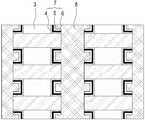
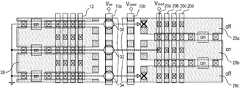
도 1은 본 발명의 일 실시예에 의한 메모리 셀 스트링 스택을 이용한 메모리 어레이의 일부에 대한 평면도로, 내부 구조를 보이기 위해 xy 평면에서 수직인 z축 방향으로 적층되며 형성된 복수개의 셀 스트링 스택들의 임의 반도체층에서 수평으로 절단한 단면도이다.
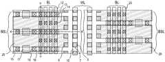
도 2는 도 1의 C 부분에 해당하는 사시도로, 본 발명의 일 실시예에 의한 메모리 셀 스트링 스택 구조를 보여준다.
도 3a 및 도 3b는 도 1의 B 부분에 해당하는 사시도로, 본 발명의 일 실시예에 의한 메모리 셀 스트링 스택을 이용한 메모리 어레이 구조의 일 예를 보여주는 것으로, 서로 반도체 기판상에 매몰 절연막이 있는지 여부만 차이점이 있다.
도 4a 내지 도 4c는 본 발명에 의한 게이트 절연막 스택의 각 실시예를 보여주기 위해 도 2 또는 도 3에서 y 방향으로 배열된 제어전극들을 지나며 절단한 단면도의 일부이다.
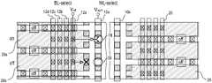
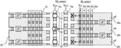
도 5, 도 8 및 도 13은 본 발명에 의한 메모리 어레이의 구조, 컨택 및 배선의 구체적인 실시예들을 보여주기 위한 레이아웃(평면도)이다.
도 6은 도 5의 XX'선을 따라 절단한 단면도이다.
도 7은 도 5의 YY'선을 따라 절단한 단면도이다.
도 9는 도 8의 XX'선을 따라 절단한 단면도이다.
도 10은 도 8의 YY'선을 따라 절단한 단면도이다.
도 11a 및 도 11b는 도 8의 메모리 어레이로 프로그램 동작을 하는 일 예를 보여주기 위한 동작 설명도이다.
도 12a 및 도 12b는 도 8의 메모리 어레이로 리드 동작을 하는 일 예를 보여주기 위한 동작 설명도이다.
도 14는 도 13의 메모리 어레이로 프로그램 동작을 하는 일 예를 보여주기 위한 동작 설명도이다.
도 15는 도 13의 메모리 어레이로 리드 동작을 하는 일 예를 보여주기 위한 동작 설명도이다.1 is a plan view of a portion of a memory array using a memory cell string stack according to an embodiment of the present invention, and any of a plurality of cell string stacks formed and stacked in the z-axis direction perpendicular to the xy plane to show an internal structure. It is sectional drawing cut horizontally in the semiconductor layer.
FIG. 2 is a perspective view corresponding to portion C of FIG. 1 and illustrates a memory cell string stack structure according to an embodiment of the present invention.
3A and 3B are perspective views corresponding to part B of FIG. 1, and show an example of a memory array structure using a memory cell string stack according to an embodiment of the present invention. There is only a difference.
4A to 4C are cross-sectional views taken through the control electrodes arranged in the y-direction in FIG. 2 or FIG. 3 to show each embodiment of the gate insulating film stack according to the present invention.
5, 8, and 13 are layouts (plan views) for showing specific embodiments of the structure, contacts, and wiring of the memory array according to the present invention.
6 is a cross-sectional view taken along the line XX ′ of FIG. 5.
FIG. 7 is a cross-sectional view taken along the line YY ′ of FIG. 5.
FIG. 9 is a cross-sectional view taken along the line XX ′ of FIG. 8.
FIG. 10 is a cross-sectional view taken along the line YY ′ of FIG. 8.
11A and 11B are explanatory diagrams illustrating an example of performing a program operation on the memory array of FIG. 8.
12A and 12B are explanatory diagrams illustrating an example of performing a read operation to the memory array of FIG. 8.
FIG. 14 is a diagram illustrating an operation of performing a program operation on the memory array of FIG. 13.
FIG. 15 is an explanatory diagram illustrating an example of performing a read operation to the memory array of FIG. 13.
이하, 첨부된 도면을 참조하며 본 발명의 바람직한 실시예에 대하여 상세히 설명한다.Hereinafter, with reference to the accompanying drawings will be described in detail a preferred embodiment of the present invention.
도 1은 본 발명의 일 실시예에 의한 메모리 셀 스트링 스택을 이용한 메모리 어레이의 일부에 대한 평면도로, 내부 구조를 보이기 위해 xy 평면에서 수직인 z축 방향으로 적층되며 형성된 복수개의 셀 스트링 스택들의 임의 반도체층에서 수평으로 절단한 단면도이다.1 is a plan view of a portion of a memory array using a memory cell string stack according to an embodiment of the present invention, and any of a plurality of cell string stacks formed and stacked in the z-axis direction perpendicular to the xy plane to show an internal structure. It is sectional drawing cut horizontally in the semiconductor layer.
도 1에서 영역 A는 하나의 메모리 셀 소자가 점유하는 면적을 표시한 것이고, 영역 B는 후술되는 메모리 어레이에 관한 각 실시예의 구조를 설명하기 위해 그 일부를 나타낸 것이고, 영역 C는 메모리 어레이를 구성하는 메모리 셀 스트링 스택의 일부를 나타낸 것이고, 우측 상단에 표시된 'F'는 주어진 기술에서의 최소 선폭을 나타낸 것이다.In FIG. 1, region A represents an area occupied by one memory cell element, and region B represents a part of the structure to explain the structure of each embodiment of the memory array described later, and region C constitutes a memory array. Shows a part of the memory cell string stack, and 'F' in the upper right corner shows the minimum line width in a given technology.
이하에서는 본 발명에 따른 실시예를 크게 메모리 셀 스트링 스택과 메모리 어레이로 나누어 설명한다.
Hereinafter, an embodiment according to the present invention will be largely divided into a memory cell string stack and a memory array.
[셀 스트링 스택에 관한Regarding Cell String Stacks실시예Example]]
우선, 본 발명의 일 실시예에 의한 셀 스트링 스택은, 도 1 및 도 2와 같이, 반도체 기판(1) 상에 절연막(2)과 반도체층(3)이 교대로 반복 적층되며 수평의 제 1 방향(예컨대, x 방향)으로 일정 길이를 갖도록 형성된 반도체 스택(40); 상기 반도체 스택(40)의 적어도 일 측면 상에 상기 제 1 방향(예컨대, x 방향)을 따라 일정 거리 이격되며 복수개 형성된 전하 저장층(5)을 포함한 게이트 절연막 스택들(7); 상기 각 게이트 절연막 스택 상에 형성된 복수개의 제어전극들(8); 및 상기 제어전극들 사이 및 상기 게이트 절연막 스택들 사이에 채워진 분리절연막(9)을 포함하여 구성되되, 상기 반도체 스택(40)의 상기 반도체층(3)은 상기 절연막(2)보다 폭이 작아 상기 게이트 절연막 스택들(7)이 형성되는 측면에 요홈이 형성되고, 상기 게이트 절연막 스택들(7)의 각 전하 저장층(5)은 상기 요홈에 형성되어 상하 메모리 셀 소자 간에 서로 분리된 것을 특징으로 한다.First, in the cell string stack according to an embodiment of the present invention, as shown in FIGS. 1 and 2, the insulating
여기서, 상기 반도체층(3)은 단결정 반도체 물질로 형성됨이 바람직하나, 다결정 또는 비정질 반도체 물질로 형성될 수도 있고, 특정 불순물이 약하게 도핑되어 있어 p형 또는 n형 반도체 바디로 기능 한다.In this case, the
그리고, 상기 반도체 스택(40)은, 도 2와 같이, 반도체 기판(1) 상에 산화막과 같은 절연막(2)을 사이에 두며 복수개의 반도체층들(3)이 수직하게 반복 적층된 것으로 수평의 제 1 방향(예컨대, x 방향)으로 일정 길이를 갖도록 형성된다.In addition, as shown in FIG. 2, the
이때, 상기 반도체 스택(40)의 각 반도체층(3)은 상하로 적층된 절연막(2)보다 폭이 작아 상기 게이트 절연막 스택들(7)이 형성되는 반도체 스택(40)의 적어도 일 측면에 수평의 제 1 방향(예컨대, x 방향)으로 요홈이 형성된다. 도 2에서는 반도체 스택의 양 측면에 요홈이 형성된 것으로 도시되었으나, 일 측면에만 요홈이 형성될 수 있다.In this case, each
상기 요홈에 상기 게이트 절연막 스택들(7)의 각 전하 저장층(5)이 형성되도록 하여 상하 메모리 셀 소자 간에 전하 저장층(5)이 서로 분리되도록 하여, 상하 셀 소자 간의 전하 저장노드(전하 저장층)에 저장된 전하의 이동을 원천 차단할 수 있게 된다.The
즉, 상기 게이트 절연막 스택(7)은 상기 반도체 스택(40)의 적어도 일 측면 상에서 터널링 절연막(4)/전하 저장층(5)/블로킹 절연막(6), 터널링 절연막(4)/전하 저장층(5) 또는 전하 저장층(5)/블로킹 절연막(6) 순으로 적층되어 형성되는데, 도 2와 같이, 상기 반도체 스택(40)의 절연막(2) 상에는 상기 게이트 절연막 스택들(7)의 각 전하 저장층(5)이 절단되어 상기 요홈에서만 상기 전하 저장층(5)이 존재하도록 하여, 상하 메모리 셀 소자 간에 전하 저장층(5)이 서로 분리되도록 한다.That is, the gate insulating
상기 게이트 절연막 스택(7)이 터널링 절연막(4)/전하 저장층(5)/블로킹 절연막(6)으로 이루어진 경우에 있어서, 상기 전하 저장층(5)이 상기 반도체 스택(40)의 절연막(2) 상에서 절단되는 구체적 실시예는 도 4a 내지 도 4c에 도시된 바와 같다.In the case where the gate insulating
도 4a는 상기 반도체 스택(40)의 절연막(2) 상에서 상기 게이트 절연막 스택(7) 중 터널링 절연막(4)/전하 저장층(5)이 절단된 모습을, 도 4b는 전하 저장층(5)/블로킹 절연막(6)이 절단된 모습을, 도 4c는 터널링 절연막(4)/전하 저장층(5)/블로킹 절연막(6) 모두 절단된 모습을 각각 보여주고 있다.FIG. 4A shows a tunneling insulating
또한, 상기 게이트 절연막 스택(7)은, 도 2와 같이, 상기 반도체 스택(40)의 적어도 일 측면 상에 상기 제 1 방향(예컨대, x 방향)을 따라 일정 거리 이격되며 복수개 형성되어, 같은 반도체층(3) 상에 형성되는 좌우 메모리 셀 소자 간에 전하 저장층(5)이 서로 분리되도록 하여, 좌우 셀 소자 간의 전하 저장노드(전하 저장층)에 저장된 전하의 이동도 원천 차단할 수 있게 하는 것이 바람직하다.In addition, as shown in FIG. 2, a plurality of gate insulating
이렇게 함으로써, 상기 전하 저장층(5)은 트랩을 가진 절연막(예컨대, 질화막)이나 나노 크기의 도트(dot)가 분산된 절연막과 같이 비전도성 물질로 형성할 수 있음은 물론 도전성 박막과 같은 전도성 물질로 형성하여 플로팅 게이트 구조를 갖는 메모리 셀 소자도 형성할 수 있게 된다.By doing so, the
그리고, 상기 복수개의 게이트 절연막 스택들(7) 중 적어도 어느 한 절연막(예컨대, 블로킹 절연막, 6)은 상기 반도체 스택(40)의 양측 반도체 기판(1) 상에도 연장 형성되도록 하여, 이를 통해 상기 제어전극들(8)과 상기 반도체 기판(1)이 서로 절연되도록 함이 바람직하다.In addition, at least one insulating layer (eg, a blocking insulating layer 6) of the plurality of gate insulating
나아가, 도 3b와 같이, 상기 반도체 스택(40) 및 상기 게이트 절연막 스택들(7)과 상기 반도체 기판(1) 사이에 매몰 절연막(11)을 더 형성하여, 상기 제어전극들(8)과 인접한 반도체 기판(1)으로 인한 누설전류의 가능성을 완전히 배제시키는 것이 바람직하다.Further, as shown in FIG. 3B, a buried insulating
그리고, 상기 복수개의 제어전극들(8)은 도전성 물질(예컨대, 도핑된 반도체 물질 또는 금속)로 상기 반도체 스택(40)의 적어도 일 측면 상에 상기 제 1 방향(예컨대, x 방향)을 따라 일정 거리 이격되며 수직한 방향으로 형성된 각 게이트 절연막 스택(7) 상에 형성되어, 상기 반도체 스택(40)의 각 반도체층(3)과 수직 교차하게 된다.The plurality of
그 결과, 상기 각 반도체층(3)의 상기 제 1 방향(예컨대, x 방향)을 따라 상기 제어전극들(8)과 수직 교차하는 위치에 메모리 셀 소자들이 형성되어, 상기 제 1 방향(예컨대, x 방향)으로 메모리 셀 스트링을 이루게 된다.As a result, memory cell elements are formed at positions perpendicular to the
이때, 상기 각 반도체층(3)에서 상기 제 1 방향(예컨대, x 방향)으로 메모리 셀 스트링을 이루는 메모리 셀 소자들은, 도 2와 같이, 상기 제어전극들(8) 사이의 상기 반도체층(3)에 불순물 도핑층으로 소스(3a, 3c)/드레인(3b, 3d)을 형성하여 서로 연결될 수도 있으나, 이웃 제어전극들(8)에 전기가 인가될 때 상기 반도체층(3)에 프린징 전계(fringing field)로 형성되는 반전층(inversion layer)이나 축적층(accumulation layer)으로 서로 연결되도록 할 수도 있다.In this case, the memory cell elements forming the memory cell string in the first direction (for example, the x direction) in each of the semiconductor layers 3 are the
전자의 경우로 반도체층(3)에 불순물 도핑층으로 소스(3a, 3c)/드레인(3b, 3d)을 형성할 때에는, 반도체층(3)에 약하게 도핑된 불순물과 반대되는 타입으로 고농도의 불순물 도핑층이 형성하도록 한다.In the former case, when the
또한, 상기 소스(3a, 3c)/드레인(3b, 3d)용 불순물 도핑층은 제조공정상 분리절연막(9)을 채우기 전에 하게 되는데, 각 반도체층(3) 양측으로 형성되는 불순물 도핑층들(예컨대, 3a와 3c 또는 3b와 3d)이 서로 만나게 할 필요는 없으나, 서로 만나게 되어도 마주보는 제어전극들(8)에 서로 다른 동작전압을 인가하게 되면 구분할 수 있게 되므로, 동작상 문제될 것은 없다.In addition, the impurity doping layers for the
다만, 상기 소스(3a, 3c)/드레인(3b, 3d)용 불순물 도핑층 형성시 이온주입후 어닐링 시간을 조절하여 상기 소스(3a, 3c)/드레인(3b, 3d)용 불순물 도핑층들이, 도 2와 같이, 제어전극들(8) 밑으로 약간 겹치게 파고들도록 형성되도록 함으로써, 이레이즈 동작시 GIDL(Gate Induced Drain Leakage)에 의하여 각 전하저장층(전하 저장노드, 5)에 저장된 것과 반대 유형의 전하를 생성하여 상기 각 전하저장층(5)에 공급할 수 있도록 함이 바람직하다.However, when forming the impurity doping layer for the source (3a, 3c) / drain (3b, 3d) by adjusting the annealing time after ion implantation, the impurity doping layers for the source (3a, 3c) / drain (3b, 3d), As shown in FIG. 2, the electrodes are formed so as to penetrate slightly under the
마지막으로, 상기 분리절연막(9)은 산화막과 같은 물질로 상기 제어전극들(8) 사이 및 상기 게이트 절연막 스택들(7) 사이에 채워지게 된다.
Finally, the
[메모리 어레이에 관한[Regarding Memory Array실시예Example]]
다음은 상기 메모리 셀 스트링 스택에 관한 실시예를 이용한 메모리 어레이에 대하여 설명한다.Next, a memory array using an embodiment of the memory cell string stack will be described.
이는, 도 1 및 도 3a와 같이, 반도체 기판(1) 상에 각각 절연막(2)과 반도체층(3)이 교대로 반복 적층되며 수평의 제 1 방향(예컨대, x 방향)으로 일정 길이를 갖고, 수평의 제 2 방향(예컨대, y 방향)으로 일정 거리 이격되며 복수개 형성된 반도체 스택들(42, 44); 상기 각 반도체 스택(42)(44)의 적어도 일 측면 상에 상기 제 1 방향(예컨대, x 방향)을 따라 일정 거리 이격되며 복수개 형성된 전하 저장층(5)을 포함한 게이트 절연막 스택들(7); 상기 각 게이트 절연막 스택(7) 상에 상기 반도체 스택들(42, 44) 사이의 이격 공간에 형성된 복수개의 제어전극들(8); 및 상기 제어전극들(8) 사이 및 상기 게이트 절연막 스택들(7) 사이에 채워진 분리절연막(9)을 포함하여 구성되되, 상기 각 반도체 스택(42)(44)의 상기 반도체층(3)은 상기 절연막(2)보다 폭이 작아 상기 게이트 절연막 스택들(7)이 형성되는 측면에 요홈이 형성되고, 상기 게이트 절연막 스택들(7)의 각 전하 저장층(5)은 상기 요홈에 형성되어 상하 메모리 셀 소자 간에 서로 분리된 것을 특징으로 한다.1 and 3A, the insulating
본 메모리 어레이에 관한 실시예는 상기에서 언급한 메모리 셀 스트링 스택에 관한 실시예가 그대로 이용되므로, 각 구성에 대한 설명 중 상기 메모리 셀 스트링 스택의 실시예에서 언급한 부분은 생략하고, 상기에서 언급되지 않은 구성을 중심으로 설명한다.In the embodiment of the present memory array, the above-described embodiment of the memory cell string stack is used as it is, and thus, the descriptions of the respective configurations of the memory cell string stack are omitted and are not mentioned above. The description focuses on the configuration.
상기 각 반도체 스택(42)(44)은 접지라인 또는 공통소스라인과 컨택되기 위하여 적어도 일단에 상기 반도체층(3)이 수평으로 돌출되도록, 즉 테라스(terrace) 구조를 이루도록, 단차를 이루며 복수개 적층되거나(미도시), 도 6과 같이, 반도체 스택 상부로 돌출되도록 연장되며 복수개 적층된다.Each of the semiconductor stacks 42 and 44 is stacked in a plurality of steps so that the
도 6은 도 5의 XX'선을 따라 절단한 단면도인데, 이에 의하면, 각 반도체 스택(42)(44)의 반도체층들(3)은 반도체 스택 상부로 돌출되도록 연장되고, 각각은 컨택(13)을 통하여 선택 트랜지스터의 드레인(24)과 소정의 배선(19)으로 연결되고, 상기 선택 트랜지스터의 소스(22)는 접지라인 또는 공통소스라인과 연결되는 일 실시예를 보여준다.FIG. 6 is a cross-sectional view taken along the line XX ′ of FIG. 5, whereby the semiconductor layers 3 of each
상기와 같이, 선택 트랜지스터가 상기 각 반도체 스택(42)(44)의 일단에 동시 형성되도록 함이 바람직하다.As described above, it is preferable that the selection transistors are simultaneously formed at one end of each of the semiconductor stacks 42 and 44.
도 6에서 미설명된 도면부호 23은 선택 트랜지스터의 게이트 절연막, 17은 선택 트랜지스터의 게이트, 16은 소스 컨택, 18은 드레인 컨택, 25는 분리 절연막, 12는 비트라인, 10은 워드라인, 그리고 27은 층간 절연막이다.In FIG. 6,
상기 실시예에 의한 메모리 어레이에 있어서, 상기 각 반도체 스택(42)(44)의 각 반도체층(3) 및 상기 제어전극들(8)이 연결되는 배선의 구체적 실시예들을 도 5, 도 8 및 도 13을 참조하며 설명하면 하기와 같다.In the memory array according to the embodiment, specific embodiments of wirings to which the semiconductor layers 3 and the
먼저, 도 5, 도 8 및 도 13에 공통적으로 도시된 바와 같이, 상기 각 반도체 스택의 각 반도체층(3)은 일단에 상기 제 1 방향(예컨대, 도 5의 XX' 방향, 도 2의 x 방향)으로 일정 거리 이격되며 상기 제 2 방향(예컨대, 도 5의 YY' 방향, 도 2의 y 방향)으로 형성된 복수개의 비트라인들(BL) 중 어느 하나와 전기적으로 연결되고, 타단에 선택 트랜지스터를 통하여 접지되고, 상기 제어전극들(8)은 상기 비트라인들(BL)과 가까운 하나 또는 둘의 상기 제 2 방향으로 형성된 것을 제외하고, 각각 상기 제 2 방향으로 형성된 복수개의 워드라인들(WL) 중 어느 하나와 전기적으로 연결되고, 상기 비트라인들(BL)과 가까운 하나 또는 둘의 상기 제 2 방향으로 형성된 제어전극들(8)은 각각 상기 제 2 방향으로 일정 거리 이격되며 상기 제 1 방향으로 형성된 복수개의 비트선택라인들(BSL) 중 어느 하나와 전기적으로 연결된다.First, as shown in FIGS. 5, 8 and 13, each
여기서, 상기 각 비트라인(BL) 및 상기 선택 트랜지스터와 연결되는 상기 각 반도체층(3)의 양단은, 도 6 및 도 9에 도시된 바와 같이, 나머지 각 메모리 셀 소자의 바디를 이루는 부분에 도핑된 불순물과 반대되는 타입의 불순물이 고농도로 도핑된 연결용 불순물 도핑층(3e)이 더 형성될 수 있는데, 이 경우 각 메모리 셀 소자의 바디는 플로팅 되게 된다.Here, both ends of each of the semiconductor layers 3 connected to the bit lines BL and the selection transistors are doped in portions forming the body of the remaining memory cell elements, as shown in FIGS. 6 and 9. A connection
구체적으로, 도 5 및 도 6과 같이, 상기 복수개의 비트라인들(BL)은 상기 복수개의 워드라인들(WL)의 좌, 우 양측으로 나누어 형성되고, 상기 복수개의 워드라인들(WL)의 좌측에 형성된 좌측 비트라인들(BL)은 각각 짝수 번째 반도체 스택들의 동일한 층에 적층된 반도체층들(3)과 연결되고, 상기 복수개의 워드라인들(WL)의 우측에 형성된 우측 비트라인들(BL)은 각각 홀수 번째 반도체 스택들의 동일한 층에 적층된 반도체층들(3)과 연결될 수 있다.In detail, as illustrated in FIGS. 5 and 6, the plurality of bit lines BL are formed by dividing the left and right sides of the plurality of word lines WL, and the plurality of word lines WL. The left bit lines BL formed at the left side are connected to the semiconductor layers 3 stacked on the same layer of even-numbered semiconductor stacks, respectively, and the right bit lines BL formed at the right side of the plurality of word lines WL are formed. BL) may be connected to the semiconductor layers 3 stacked on the same layer of odd-numbered semiconductor stacks, respectively.
여기서, 상기 복수개의 비트선택라인들(BSL)은, 도 5 및 도 7과 같이, 상기 복수개의 워드라인들(WL)의 좌, 우 양측으로 나누어 형성되고, 상기 복수개의 워드라인들의 좌측에 형성된 좌측 비트선택라인들(BSL, 15)은 각각 층간절연막(27)을 사이에 두고 상기 좌측 비트라인들(12)과 수직으로 교차하며 상기 좌측 비트라인들(12)과 가까운 하나의 상기 제 2 방향으로 형성된 제어전극들(8) 중 어느 하나와 연결되고, 상기 복수개의 워드라인들(WL)의 우측에 형성된 우측 비트선택라인들(BSL, 21)은 각각 층간절연막(27)을 사이에 두고 상기 우측 비트라인들(BL)과 수직으로 교차하며 상기 우측 비트라인들(BL)과 가까운 하나의 상기 제 2 방향으로 형성된 제어전극들(8) 중 어느 하나와 연결될 수 있다.Here, the plurality of bit select lines BSL are formed by dividing the left and right sides of the plurality of word lines WL, as shown in FIGS. 5 and 7, and formed on the left side of the plurality of word lines. The left bit select lines BSL 15 intersect the
도 5에서 각 비트라인(BL)이 동일한 층에 적층된 반도체층들(3)과 전기적으로 연결되는 부분은 각 비트라인(BL) 상에 실선으로 컨택 표시(14)를 하였고, 각 비트라인(BL) 하측에서 각 반도체층(3)이 선택 트랜지스터의 드레인(24)과 소정의 배선(19)으로 연결되는 부분은 각 비트라인(BL) 상에 점선으로 컨택 표시(13)를 하였다.In FIG. 5, the portions in which the bit lines BL are electrically connected to the semiconductor layers 3 stacked on the same layer have contact marks 14 in solid lines on the bit lines BL. A portion of the
다른 배선의 예로, 도 8 내지 도 10과 같이, 상기 복수개의 비트선택라인들BSL)은 상기 복수개의 워드라인들(WL)의 좌, 우 양측으로 나누어 형성되고, 상기 복수개의 워드라인들(WL)의 좌측에 형성된 좌측 비트선택라인들(28)은 각각 층간절연막(27)을 사이에 두고 상기 좌측 비트라인들(12)과 수직으로 교차하며 상기 좌측 비트라인들(12)과 가까운 하나의 상기 제 2 방향으로 형성된 제어전극들(8) 중 이웃한 두 개와 연결되고, 상기 복수개의 워드라인들(WL)의 우측에 형성된 우측 비트선택라인들(29)은 각각 층간절연막(27)을 사이에 두고 상기 우측 비트라인들(20)과 수직으로 교차하며 상기 우측 비트라인들(20)과 가까운 하나의 상기 제 2 방향으로 형성된 제어전극들(8) 중 이웃한 두 개와 연결되되, 상기 좌측 비트선택라인들(28) 및 상기 우측 비트선택라인들(29)의 중심이 서로 엇갈리게 형성되도록 할 수 있다.As another wiring example, as shown in FIGS. 8 to 10, the plurality of bit selection lines BSL are formed by dividing the left and right sides of the plurality of word lines WL, and the plurality of word lines WL. The left bit
도 8에서도 각 비트라인(BL)이 동일한 층에 적층된 반도체층들(3)과 전기적으로 연결되는 부분은 각 비트라인(BL) 상에 실선으로 컨택 표시(14)를 하였고, 각 비트라인(BL) 하측에서 각 반도체층(3)이 선택 트랜지스터의 드레인(24)과 소정의 배선(19)으로 연결되는 부분은 각 비트라인(BL) 상에 점선으로 컨택 표시(13)를 하였다.In FIG. 8, the portion in which each bit line BL is electrically connected to the semiconductor layers 3 stacked on the same layer has a
도 8과 같이 배선이 형성되었을 때, 프로그램 동작은 도 11a 및 도 11b와 같이, 리드 동작은 도 12a 및 도 12b와 같이 실시할 수 있다.When the wiring is formed as shown in FIG. 8, the program operation may be performed as shown in FIGS. 11A and 11B and the read operation may be performed as shown in FIGS. 12A and 12B.
즉, 도 11a에서 특정 메모리 셀 소자(31)를 프로그램시키기 위하여, 접지라인 또는 공통소스라인과 연결되는 양측의 모든 선택 트랜지스터들의 게이트에는 채널이 형성되지 않을 오프(off) 전압을 인가하고, 상기 특정 메모리 셀 소자(31)가 형성되는 반도체층(3)이 포함된 반도체 스택 위를 지나는 비트선택라인(28a)은 이에 연결된 제어전극들(8)과 접하는 반도체층(3)에 채널이 형성될 정도로 온(on) 전압을 인가하고 좌측 나머지 비트선택라인들(28b) 또는 모든 나머지 비트선택라인들(28b, 29)은 오프(off) 전압을 인가한다.That is, in order to program the specific
상기 상태에서 상기 특정 메모리 셀 소자(31)가 형성된 반도체층(3)의 연결용 불순물 도핑층과 전기적으로 연결된 비트라인(12a)을 선택하여 기준 전압(Vref, 예컨대 접지)을 인가하고 나머지 비트라인들(12b, 12c, 12d, 20)은 플로팅 시킨 다음, 상기 특정 메모리 셀 소자(31)의 게이트를 형성하는 제어전극들(8)과 전기적으로 연결된 워드라인(10a)을 선택하여 프로그램 전압(Vpgm)을 인가하고 나머지 워드라인들(10b)은 턴 온(turn on)될 정도의 패스전압(Vpass)을 인가한다.In this state, the
상기와 같이 동작시킬 때, 선택된 비트라인(12a)에 함께 연결된 메모리 셀 소자(33)의 반도체층에는 오프 전압이 인가된 비트선택라인(28b)에 의하여 채널이 형성하지 않게 되므로(도 11a에서 'X'로 표시됨), 상기 메모리 셀 소자(33)에는 프로그램되지 않게 된다.In the operation as described above, the channel is not formed in the semiconductor layer of the
그리고, 상기 특정 메모리 셀 소자(31)와 이웃한 메모리 셀 소자(32)를 프로그램시키고자 할 경우에는, 도 11b와 같이, 동작시키면 되고, 구체적인 방법은 상기 특정 메모리 셀 소자(31)를 프로그램시킬 경우와 동일하다.When the specific
한편, 도 12a에서 특정 메모리 셀 소자(31)를 리드(읽기) 하기 위해서는, 선택 트랜지스터들은 모두 온(on) 전압을 인가하고, 우측 비트선택라인들은 모두 온(on) 전압을 인가하고, 좌측 비트선택라인들은 상기 특정 메모리 셀 소자(31)가 형성되는 반도체층(3)이 포함된 반도체 스택 위를 지나는 비트선택라인(28a)만 온(on) 전압을, 나머지(28b)는 오프(off) 전압을 각각 인가한다.Meanwhile, in order to read (read) the specific
상기 상태에서 상기 특정 메모리 셀 소자(31)가 형성된 반도체층(3)의 연결용 불순물 도핑층과 전기적으로 연결된 비트라인(12a)을 선택하여 리드 전압(Vread)을 인가하고 나머지 비트라인들(12b, 12c, 12d, 20)은 플로팅 시킨 다음, 상기 특정 메모리 셀 소자(31)의 게이트를 형성하는 제어전극들(8)과 전기적으로 연결된 워드라인(10a)을 선택하여 특정 전압(Vsel)을 인가하고 나머지 워드라인들(10b)은 턴 온(turn on)될 정도의 전압(Vunsel)을 인가한다.In this state, the
상기와 같이 동작시킬 때, 선택된 비트라인(12a)에 함께 연결된 메모리 셀 소자(33)의 반도체층에는 오프 전압이 인가된 비트선택라인(28b)에 의하여 채널이 형성하지 않게 되므로(도 12a에서 'X'로 표시됨), 상기 메모리 셀 소자(33)에는 리드 전류가 흐르지 않게 된다.In the above operation, the channel is not formed in the semiconductor layer of the
그리고, 상기 특정 메모리 셀 소자(31)와 이웃한 메모리 셀 소자(32)를 리드(읽기) 하고자 할 경우에는, 도 12b와 같이, 동작시키면 되고, 구체적인 방법은 상기 특정 메모리 셀 소자(31)를 리드(읽기) 할 경우와 동일하다.In addition, when the
상기와 같이, 도 8과 같은 배선 구조에서 프로그램 동작을 시킬 경우, 도 11a 및 도 11b와 같이, 각 반도체층(3)의 양측에 형성된 게이트 절연막 스택들(7)의 각 전하 저장층(5)에 전자를 넣게 되고, 리드 동작의 경우에도, 도 12a 및 도 12b와 같이, 각 반도체층(3)의 양측의 전하 저장층들(5)에 저장된 상태를 센싱하게 된다. 따라서, 이 경우 각 메모리 셀 소자는 반도체층(3)을 바디로 하고 전하 저장층(5) 및 게이트를 각각 2개 갖는 구조로 동작하게 된다.As described above, when the program operation is performed in the wiring structure as shown in FIG. 8, as shown in FIGS. 11A and 11B, each
한편, 도 5와 같은 배선 구조에서 동작시킬 경우, 각 메모리 셀 소자는 반도체층(3)을 바디로 하고 하나의 전하 저장층(5)과 하나의 게이트(제어전극: 8)를 갖는 구조로 동작시킬 수 있으므로, 집적도 측면에서 도 5와 같이 배선 구조를 형성함이 보다 바람직하나, 각 비트선택라인(BSL)을 구동하기 위한 수단이 더 증가되는 단점이 있다.On the other hand, when operating in the wiring structure as shown in FIG. 5, each memory cell element operates as a structure having the
또 다른 배선의 예로, 도 13과 같이, 상기 복수개의 비트라인들(BL, 36)은 상기 복수개의 워드라인들(WL)의 좌측 또는 우측에 형성되어 각각 상기 반도체 스택들의 동일한 층에 적층된 반도체층들(3)과 연결되고, 상기 복수개의 비트선택라인들(BSL)은 각각 층간절연막을 사이에 두고 상기 비트라인들(36)과 수직으로 교차하며 상기 비트라인들과 가까운 둘의 상기 제 2 방향으로 형성된 제어전극들(8) 중 사선으로 위치한 두 개의 제어전극들(8a, 8b)과 연결될 수 있다.As another wiring example, as illustrated in FIG. 13, the plurality of bit lines BL and 36 are formed on the left or right side of the plurality of word lines WL, respectively, and are stacked on the same layer of the semiconductor stacks. Two second bit select lines BSL connected to the
도 13과 같이 배선이 형성되었을 때, 프로그램 동작은 도 14와 같이, 리드 동작은 도 15와 같이 실시할 수 있다.When the wiring is formed as shown in FIG. 13, the program operation may be performed as shown in FIG. 14, and the read operation may be performed as shown in FIG. 15.
즉, 도 14에서 특정 메모리 셀 소자(32)를 프로그램시키기 위하여, 접지라인 또는 공통소스라인과 연결되는 모든 선택 트랜지스터들의 게이트에는 채널이 형성되지 않을 오프(off) 전압을 인가하고, 상기 특정 메모리 셀 소자(31)가 형성되는 반도체층(3)이 포함된 반도체 스택 아래로 이웃한 비트선택라인(35d)은 이에 사선으로 연결된 제어전극들(8)과 접하는 반도체층(3)에 채널이 형성될 정도로 온(on) 전압을 인가하고 나머지 비트선택라인들(35a, 35b, 35c, 35e, 35f)은 오프(off) 전압을 인가한다.That is, in order to program the specific
상기 상태에서 상기 특정 메모리 셀 소자(32)가 형성된 반도체층(3)의 연결용 불순물 도핑층과 전기적으로 연결된 비트라인을 선택하여 기준 전압(Vref, 예컨대 접지)을 인가하고 나머지 비트라인들은 플로팅 시킨 다음, 상기 특정 메모리 셀 소자(32)의 게이트를 형성하는 제어전극들(8)과 전기적으로 연결된 워드라인(10a)을 선택하여 프로그램 전압(Vpgm)을 인가하고 나머지 워드라인들(10b)은 턴 온(turn on)될 정도의 패스전압(Vpass)을 인가한다.In this state, a bit line electrically connected to an impurity doping layer for connecting the
상기와 같이 동작시킬 때, 선택된 비트라인에 함께 연결된 메모리 셀 소자들의 각 반도체층에는 오프 전압이 인가된 비트선택라인에 의하여 채널이 형성하지 않게 되므로(도 14에서 'X'로 표시됨), 이들 메모리 셀 소자에는 프로그램되지 않게 된다.In the operation as described above, since the channel is not formed by the bit select line to which the off voltage is applied to each semiconductor layer of the memory cell elements connected to the selected bit line (indicated by 'X' in FIG. 14), these memories It is not programmed in the cell device.
한편, 도 15에서 특정 메모리 셀 소자(32)를 리드(읽기) 하기 위해서는, 선택 트랜지스터들 중 상기 특정 메모리 셀 소자(32)가 형성되는 반도체층(3)이 연결된 선택 트랜지스터(17c)만 온(on) 전압을 인가하고 나머지 선택 트랜지스터들(17a, 17b, 17d, 17e)은 오프(off) 전압을 인가하고, 비트선택라인들(35a, 35b, 35c, 35d, 35e, 35f)은 모두 온(on) 전압을 인가한다.Meanwhile, in order to read (read) the specific
상기 상태에서 상기 특정 메모리 셀 소자(32)가 형성된 반도체층(3)의 연결용 불순물 도핑층과 전기적으로 연결된 비트라인(36a)을 선택하여 리드 전압(Vread)을 인가하고 나머지 비트라인들(36b, 36c, 36d)은 플로팅 시킨 다음, 상기 특정 메모리 셀 소자(32)의 게이트를 형성하는 제어전극들(8)과 전기적으로 연결된 워드라인(10a)을 선택하여 특정 전압(Vsel)을 인가하고 나머지 워드라인들(10b)은 턴 온(turn on)될 정도의 전압(Vunsel)을 인가한다.In this state, the
상기와 같이 동작시킬 때, 선택된 비트라인(36a)에 함께 연결된 메모리 셀 소자들의 각 반도체층에는 오프 전압이 인가된 선택 트랜지스터들(17a, 17b, 17d, 17e)에 의하여 전도 경로가 형성되지 않게 된다.In the operation as described above, the conductive path is not formed by the
1: 반도체 기판
2: 절연막
3: 반도체층
4: 터널링 절연막
5: 전하 저장층
6: 블로킹 절연막
7; 게이트 절연막 스택
8: 제어전극
9: 분리절연막
10: 워드라인
12, 20, 36: 비트라인
11: 매몰절연막
13: 반도체층과 선택 트랜지스터의 드레인 컨택
14, 37: 반도체층과 비트라인 컨택
15, 21, 28, 29, 35: 비트선택라인
16: 선택 트랜지스터의 소스와 접지라인 컨택
17: 선택 트랜지스터
40, 42, 44: 반도체 스택1: semiconductor substrate
2: insulation film
3: semiconductor layer
4: tunneling insulation film
5: charge storage layer
6: blocking insulating film
7; Gate insulating film stack
8: control electrode
9: Separation insulation film
10: wordline
12, 20, 36: bitline
11: investment insulation film
13: Drain contact between semiconductor layer and select transistor
14, 37: semiconductor layer and bit line contact
15, 21, 28, 29, 35: bit select line
16: Source and Ground Line Contacts of Selected Transistors
17: select transistor
40, 42, 44: semiconductor stack
Claims (18)
Translated fromKorean상기 각 반도체 스택의 적어도 일 측면 상에 상기 제 1 방향을 따라 일정 거리 이격되며 복수개 형성된 전하 저장층을 포함한 게이트 절연막 스택들;
상기 각 게이트 절연막 스택 상에 상기 반도체 스택들 사이의 이격 공간에 형성된 복수개의 제어전극들; 및
상기 제어전극들 사이 및 상기 게이트 절연막 스택들 사이에 채워진 분리절연막을 포함하여 구성되되,
상기 각 반도체 스택의 각 반도체층은 일단에 상기 제 1 방향으로 일정 거리 이격되며 상기 제 2 방향으로 형성된 복수개의 비트라인들 중 어느 하나와 전기적으로 연결되고, 타단에 선택 트랜지스터를 통하여 접지되고,
상기 제어전극들은 상기 비트라인들과 가까운 하나 또는 둘의 상기 제 2 방향으로 형성된 것을 제외하고, 각각 상기 제 2 방향으로 형성된 복수개의 워드라인들 중 어느 하나와 전기적으로 연결되고,
상기 비트라인들과 가까운 하나 또는 둘의 상기 제 2 방향으로 형성된 제어전극들은 각각 상기 제 2 방향으로 일정 거리 이격되며 상기 제 1 방향으로 형성된 복수개의 비트선택라인들 중 어느 하나와 전기적으로 연결된 것을 특징으로 하는 메모리 어레이.
A plurality of semiconductor stacks each having an insulating layer and a semiconductor layer repeatedly alternately stacked on the semiconductor substrate, the semiconductor stacks having a predetermined length in a horizontal first direction, spaced a predetermined distance in a horizontal second direction;
Gate insulating layer stacks including a plurality of charge storage layers spaced apart at a predetermined distance along the first direction on at least one side of each semiconductor stack;
A plurality of control electrodes formed in the spaced spaces between the semiconductor stacks on the gate insulating film stacks; And
A separation insulating film filled between the control electrodes and between the gate insulating film stacks,
Each semiconductor layer of each of the semiconductor stacks is spaced apart at a distance in the first direction at one end thereof and electrically connected to any one of the plurality of bit lines formed in the second direction, and is grounded through a selection transistor at the other end thereof.
The control electrodes are electrically connected to any one of a plurality of word lines formed in the second direction, except that the control electrodes are formed in one or two second directions close to the bit lines.
Control electrodes formed in one or two second directions close to the bit lines are spaced apart from each other in the second direction by a predetermined distance and electrically connected to any one of a plurality of bit selection lines formed in the first direction. Memory array.
상기 게이트 절연막 스택들은 상기 각 반도체 스택의 양 측면 상에 상기 제 1 방향을 따라 일정 거리 이격되며 복수개 형성된 것을 특징으로 하는 메모리 어레이.
The method of claim 7, wherein
And a plurality of gate insulating layer stacks spaced apart from each other by a predetermined distance on both sides of each of the semiconductor stacks along the first direction.
상기 각 반도체 스택 및 상기 게이트 절연막 스택들과 상기 반도체 기판 사이에 매몰 절연막이 더 형성된 것을 특징으로 하는 메모리 어레이.
The method of claim 8,
And a buried insulating film is formed between the semiconductor stack and the gate insulating film stacks and the semiconductor substrate.
상기 각 반도체 스택의 상기 반도체층은 상기 절연막보다 폭이 작아 상기 게이트 절연막 스택들이 형성되는 측면에 요홈이 형성되고,
상기 각 게이트 절연막 스택은 상기 요홈 상에 터널링 절연막/상기 전하 저장층/블로킹 절연막으로 형성되고,
상기 전하 저장층은 도전성 박막, 트랩을 가진 절연막, 나노 크기의 도트(dot)가 분산된 절연막 중 어느 하나로, 상기 요홈에 형성되어 상하 메모리 셀 소자 간에 서로 분리된 것을 특징으로 하는 메모리 어레이.
The method according to any one of claims 7 to 9,
The semiconductor layer of each of the semiconductor stacks has a width smaller than that of the insulating film, and grooves are formed on the side surfaces of the gate insulating film stacks.
Each gate insulating film stack is formed of a tunneling insulating film / the charge storage layer / blocking insulating film on the groove,
The charge storage layer is any one of a conductive thin film, an insulating film having a trap, and an insulating film in which nano-sized dots are dispersed, and is formed in the groove, and the memory array, characterized in that separated from each other between the upper and lower memory cell elements.
상기 반도체층의 상기 제 1 방향을 따라 상기 제어전극들과 교차하는 위치에 메모리 셀 소자들이 형성되고,
상기 메모리 셀 소자들은 상기 반도체층에 상기 제어전극들로부터의 프린징 전계(fringing field)에 의해 형성되는 반전층(inversion layer)이나 축적층(accumulation layer)으로 서로 연결되어 메모리 셀 스트링을 이루는 것을 특징으로 하는 메모리 어레이.
The method of claim 10,
Memory cell elements are formed at positions crossing the control electrodes along the first direction of the semiconductor layer,
The memory cell elements may be connected to each other by an inversion layer or an accumulation layer formed by a fringing field from the control electrodes in the semiconductor layer to form a memory cell string. Memory array.
상기 반도체층의 상기 제 1 방향을 따라 상기 제어전극들과 교차하는 위치에 메모리 셀 소자들이 형성되고,
상기 메모리 셀 소자들은 상기 제어전극들 사이의 상기 반도체층에 불순물 도핑층으로 소스/드레인이 형성되어 서로 연결되며 메모리 셀 스트링을 이루는 것을 특징으로 하는 메모리 어레이.
The method of claim 10,
Memory cell elements are formed at positions crossing the control electrodes along the first direction of the semiconductor layer,
And the memory cell elements are connected to each other by forming a source / drain in the semiconductor layer between the control electrodes as an impurity doping layer and forming a memory cell string.
상기 각 반도체 스택은 적어도 일단에 상기 반도체층이 수평으로 돌출되도록 단차를 이루며 복수개 적층되거나, 반도체 스택 상부로 돌출되도록 연장되며 복수개 적층된 것을 특징으로 하는 메모리 어레이.
The method of claim 12,
Wherein each of the semiconductor stacks has a plurality of stacks formed at a step such that the semiconductor layers protrude horizontally at least one end thereof, or a plurality of stacked stacks extending to protrude above the semiconductor stack.
상기 복수개의 비트라인들은 상기 복수개의 워드라인들의 좌, 우 양측으로 나누어 형성되고,
상기 복수개의 워드라인들의 좌측에 형성된 좌측 비트라인들은 각각 짝수 번째 반도체 스택들의 동일한 층에 적층된 반도체층들과 연결되고,
상기 복수개의 워드라인들의 우측에 형성된 우측 비트라인들은 각각 홀수 번째 반도체 스택들의 동일한 층에 적층된 반도체층들과 연결된 것을 특징으로 하는 메모리 어레이.
The method of claim 7, wherein
The plurality of bit lines are formed by dividing the left and right sides of the plurality of word lines.
Left bit lines formed on the left side of the plurality of word lines are connected to semiconductor layers stacked on the same layer of even-numbered semiconductor stacks, respectively.
And right bit lines formed at right sides of the plurality of word lines are connected to semiconductor layers stacked on the same layer of odd-numbered semiconductor stacks, respectively.
상기 복수개의 비트선택라인들은 상기 복수개의 워드라인들의 좌, 우 양측으로 나누어 형성되고,
상기 복수개의 워드라인들의 좌측에 형성된 좌측 비트선택라인들은 각각 층간절연막을 사이에 두고 상기 좌측 비트라인들과 수직으로 교차하며 상기 좌측 비트라인들과 가까운 하나의 상기 제 2 방향으로 형성된 제어전극들 중 어느 하나와 연결되고,
상기 복수개의 워드라인들의 우측에 형성된 우측 비트선택라인들은 각각 층간절연막을 사이에 두고 상기 우측 비트라인들과 수직으로 교차하며 상기 우측 비트라인들과 가까운 하나의 상기 제 2 방향으로 형성된 제어전극들 중 어느 하나와 연결된 것을 특징으로 하는 메모리 어레이.
The method of claim 15,
The plurality of bit selection lines are formed by dividing the left and right sides of the plurality of word lines.
Left bit select lines formed on the left side of the plurality of word lines may each intersect the left bit lines vertically with an interlayer insulating layer therebetween and may be formed in one second direction close to the left bit lines. Connected to either one,
The right bit select lines formed on the right side of the plurality of word lines may each intersect the right bit lines perpendicularly to each other with the interlayer insulating layer therebetween and may be formed in one second direction close to the right bit lines. Memory array, characterized in that connected to any one.
상기 복수개의 비트선택라인들은 상기 복수개의 워드라인들의 좌, 우 양측으로 나누어 형성되고,
상기 복수개의 워드라인들의 좌측에 형성된 좌측 비트선택라인들은 각각 층간절연막을 사이에 두고 상기 좌측 비트라인들과 수직으로 교차하며 상기 좌측 비트라인들과 가까운 하나의 상기 제 2 방향으로 형성된 제어전극들 중 이웃한 두 개와 연결되고,
상기 복수개의 워드라인들의 우측에 형성된 우측 비트선택라인들은 각각 층간절연막을 사이에 두고 상기 우측 비트라인들과 수직으로 교차하며 상기 우측 비트라인들과 가까운 하나의 상기 제 2 방향으로 형성된 제어전극들 중 이웃한 두 개와 연결되되,
상기 좌측 비트선택라인들 및 상기 우측 비트선택라인들의 중심이 서로 엇갈리게 형성된 것을 특징으로 하는 메모리 어레이.
The method of claim 15,
The plurality of bit selection lines are formed by dividing the left and right sides of the plurality of word lines.
Left bit select lines formed on the left side of the plurality of word lines may each intersect the left bit lines vertically with an interlayer insulating layer therebetween and may be formed in one second direction close to the left bit lines. Connected to two neighbors,
The right bit select lines formed on the right side of the plurality of word lines may each intersect the right bit lines perpendicularly to each other with the interlayer insulating layer therebetween and may be formed in one second direction close to the right bit lines. Connected to two neighbors,
And the centers of the left bit select lines and the right bit select lines are staggered from each other.
상기 복수개의 비트라인들은 상기 복수개의 워드라인들의 좌측 또는 우측에 형성되어 각각 상기 반도체 스택들의 동일한 층에 적층된 반도체층들과 연결되고,
상기 복수개의 비트선택라인들은 각각 층간절연막을 사이에 두고 상기 비트라인들과 수직으로 교차하며 상기 비트라인들과 가까운 둘의 상기 제 2 방향으로 형성된 제어전극들 중 사선으로 위치한 두 개의 제어전극들과 연결된 것을 특징으로 하는 메모리 어레이.The method of claim 7, wherein
The plurality of bit lines may be formed on the left side or the right side of the plurality of word lines, respectively, and are connected to semiconductor layers stacked on the same layer of the semiconductor stacks.
The plurality of bit selection lines may include two control electrodes disposed diagonally among the control electrodes formed in the second direction, which are perpendicular to the bit lines and intersect the bit lines with an interlayer insulating layer therebetween. And a memory array connected thereto.
Priority Applications (1)
| Application Number | Priority Date | Filing Date | Title |
|---|---|---|---|
| KR1020100099171AKR101091023B1 (en) | 2010-10-12 | 2010-10-12 | Memory Cell String Stacks and Memory Arrays Using the Same |
Applications Claiming Priority (1)
| Application Number | Priority Date | Filing Date | Title |
|---|---|---|---|
| KR1020100099171AKR101091023B1 (en) | 2010-10-12 | 2010-10-12 | Memory Cell String Stacks and Memory Arrays Using the Same |
Publications (1)
| Publication Number | Publication Date |
|---|---|
| KR101091023B1true KR101091023B1 (en) | 2011-12-09 |
Family
ID=45505845
Family Applications (1)
| Application Number | Title | Priority Date | Filing Date |
|---|---|---|---|
| KR1020100099171AActiveKR101091023B1 (en) | 2010-10-12 | 2010-10-12 | Memory Cell String Stacks and Memory Arrays Using the Same |
Country Status (1)
| Country | Link |
|---|---|
| KR (1) | KR101091023B1 (en) |
Cited By (2)
| Publication number | Priority date | Publication date | Assignee | Title |
|---|---|---|---|---|
| US9019739B2 (en) | 2013-01-11 | 2015-04-28 | Samsung Electronics Co., Ltd. | Three-dimensional semiconductor devices and methods of fabricating the same |
| KR20180042731A (en)* | 2016-10-18 | 2018-04-26 | 부산대학교 산학협력단 | Reisistive random access memory device and method for fabricating the same |
- 2010
- 2010-10-12KRKR1020100099171Apatent/KR101091023B1/enactiveActive
Cited By (3)
| Publication number | Priority date | Publication date | Assignee | Title |
|---|---|---|---|---|
| US9019739B2 (en) | 2013-01-11 | 2015-04-28 | Samsung Electronics Co., Ltd. | Three-dimensional semiconductor devices and methods of fabricating the same |
| US9224429B2 (en) | 2013-01-11 | 2015-12-29 | Samsung Electronics Co., Ltd. | Three-dimensional semiconductor devices and methods of fabricating the same |
| KR20180042731A (en)* | 2016-10-18 | 2018-04-26 | 부산대학교 산학협력단 | Reisistive random access memory device and method for fabricating the same |
Similar Documents
| Publication | Publication Date | Title |
|---|---|---|
| US9859004B1 (en) | Three-dimensional NAND non-volatile memory and dram memory devices on a single substrate | |
| US8426976B2 (en) | Non-volatile semiconductor storage device and method of manufacturing the same | |
| US7936003B2 (en) | Semiconductor device having transistor with vertical gate electrode and method of fabricating the same | |
| US7906397B2 (en) | Methods of fabricating nonvolatile semiconductor memory devices including a plurality of stripes having impurity layers therein | |
| US8154068B2 (en) | Non-volatile semiconductor storage device and method of manufacturing the same | |
| US7135726B2 (en) | Semiconductor memory and its production process | |
| KR101160185B1 (en) | 3d vertical type memory cell string with shield electrode, memory array using the same and fabrication method thereof | |
| US20130215684A1 (en) | Nonvolatile memory device, method for operating the same, and method for fabricating the same | |
| KR101056113B1 (en) | 3D vertical memory cell string having a shielding electrode surrounded by an isolation insulating film stack, a memory array using the same, and a method of manufacturing the same | |
| CN111326521B (en) | Three-dimensional semiconductor memory device | |
| JP3566944B2 (en) | Semiconductor storage device and method of manufacturing the same | |
| CN102956644B (en) | There is nonvolatile semiconductor memory member and the manufacture method thereof of vertical memory cell | |
| JP2006186378A (en) | NOR type flash memory device having twin bit cell structure and manufacturing method thereof | |
| CN103872057A (en) | Non-volatile memory device and method of fabricating the same | |
| US20110012188A1 (en) | Semiconductor memory device | |
| KR101329586B1 (en) | 3d vertical type memory cell string with weighting electrode, memory array using the same and fabrication method thereof | |
| KR100391984B1 (en) | Semiconductor memory device having multiple tunnel junction layer pattern and method of fabricating the same | |
| KR101002293B1 (en) | Stacked nonvolatile memory cell device having a floating body, nonvolatile memory cell stack using the cell device, nonvolatile memory cell string, nonvolatile memory cell array and manufacturing method thereof | |
| KR100471183B1 (en) | Semiconductor memory device having offset transistor and method of fabricating the same | |
| JP4391741B2 (en) | Semiconductor memory device and manufacturing method thereof | |
| KR20230079248A (en) | Ferroelectric memory device containing word lines and pass gates and method of forming the same | |
| CN1828900B (en) | Semiconductor device having transistor with vertical gate electrode and method of fabricating the same | |
| KR101073640B1 (en) | High-density vertical-type semiconductor memory cell string, cell string array and fabricating method thereof | |
| KR101362219B1 (en) | Memory cell string stack with common body and memory array using the same | |
| KR101091023B1 (en) | Memory Cell String Stacks and Memory Arrays Using the Same |
Legal Events
| Date | Code | Title | Description |
|---|---|---|---|
| A201 | Request for examination | ||
| PA0109 | Patent application | Patent event code:PA01091R01D Comment text:Patent Application Patent event date:20101012 | |
| PA0201 | Request for examination | ||
| E902 | Notification of reason for refusal | ||
| PE0902 | Notice of grounds for rejection | Comment text:Notification of reason for refusal Patent event date:20110919 Patent event code:PE09021S01D | |
| E701 | Decision to grant or registration of patent right | ||
| PE0701 | Decision of registration | Patent event code:PE07011S01D Comment text:Decision to Grant Registration Patent event date:20111130 | |
| GRNT | Written decision to grant | ||
| PR0701 | Registration of establishment | Comment text:Registration of Establishment Patent event date:20111201 Patent event code:PR07011E01D | |
| PR1002 | Payment of registration fee | Payment date:20111201 End annual number:3 Start annual number:1 | |
| PG1601 | Publication of registration | ||
| FPAY | Annual fee payment | Payment date:20141128 Year of fee payment:4 | |
| PR1001 | Payment of annual fee | Payment date:20141128 Start annual number:4 End annual number:4 | |
| FPAY | Annual fee payment | Payment date:20151126 Year of fee payment:5 | |
| PR1001 | Payment of annual fee | Payment date:20151126 Start annual number:5 End annual number:5 | |
| FPAY | Annual fee payment | Payment date:20160222 Year of fee payment:6 | |
| PR1001 | Payment of annual fee | Payment date:20160222 Start annual number:6 End annual number:6 | |
| FPAY | Annual fee payment | Payment date:20171124 Year of fee payment:7 | |
| PR1001 | Payment of annual fee | Payment date:20171124 Start annual number:7 End annual number:7 | |
| FPAY | Annual fee payment | Payment date:20181203 Year of fee payment:8 | |
| PR1001 | Payment of annual fee | Payment date:20181203 Start annual number:8 End annual number:8 | |
| PR1001 | Payment of annual fee | Payment date:20201207 Start annual number:10 End annual number:10 | |
| PR1001 | Payment of annual fee | Payment date:20220413 Start annual number:11 End annual number:11 | |
| PR1001 | Payment of annual fee | Payment date:20221122 Start annual number:12 End annual number:12 |