KR101084411B1 - Capacitively Coupled Power Supplies - Google Patents
Capacitively Coupled Power SuppliesDownload PDFInfo
- Publication number
- KR101084411B1 KR101084411B1KR1020057006633AKR20057006633AKR101084411B1KR 101084411 B1KR101084411 B1KR 101084411B1KR 1020057006633 AKR1020057006633 AKR 1020057006633AKR 20057006633 AKR20057006633 AKR 20057006633AKR 101084411 B1KR101084411 B1KR 101084411B1
- Authority
- KR
- South Korea
- Prior art keywords
- capacitor
- voltage
- power supply
- switch
- delete delete
- Prior art date
- Legal status (The legal status is an assumption and is not a legal conclusion. Google has not performed a legal analysis and makes no representation as to the accuracy of the status listed.)
- Expired - Fee Related
Links
Images


Classifications
- H—ELECTRICITY
- H02—GENERATION; CONVERSION OR DISTRIBUTION OF ELECTRIC POWER
- H02M—APPARATUS FOR CONVERSION BETWEEN AC AND AC, BETWEEN AC AND DC, OR BETWEEN DC AND DC, AND FOR USE WITH MAINS OR SIMILAR POWER SUPPLY SYSTEMS; CONVERSION OF DC OR AC INPUT POWER INTO SURGE OUTPUT POWER; CONTROL OR REGULATION THEREOF
- H02M3/00—Conversion of DC power input into DC power output
- H02M3/02—Conversion of DC power input into DC power output without intermediate conversion into AC
- H02M3/04—Conversion of DC power input into DC power output without intermediate conversion into AC by static converters
- H02M3/10—Conversion of DC power input into DC power output without intermediate conversion into AC by static converters using discharge tubes with control electrode or semiconductor devices with control electrode
- H02M3/145—Conversion of DC power input into DC power output without intermediate conversion into AC by static converters using discharge tubes with control electrode or semiconductor devices with control electrode using devices of a triode or transistor type requiring continuous application of a control signal
- H02M3/155—Conversion of DC power input into DC power output without intermediate conversion into AC by static converters using discharge tubes with control electrode or semiconductor devices with control electrode using devices of a triode or transistor type requiring continuous application of a control signal using semiconductor devices only
- H02M3/156—Conversion of DC power input into DC power output without intermediate conversion into AC by static converters using discharge tubes with control electrode or semiconductor devices with control electrode using devices of a triode or transistor type requiring continuous application of a control signal using semiconductor devices only with automatic control of output voltage or current, e.g. switching regulators
- H—ELECTRICITY
- H02—GENERATION; CONVERSION OR DISTRIBUTION OF ELECTRIC POWER
- H02M—APPARATUS FOR CONVERSION BETWEEN AC AND AC, BETWEEN AC AND DC, OR BETWEEN DC AND DC, AND FOR USE WITH MAINS OR SIMILAR POWER SUPPLY SYSTEMS; CONVERSION OF DC OR AC INPUT POWER INTO SURGE OUTPUT POWER; CONTROL OR REGULATION THEREOF
- H02M1/00—Details of apparatus for conversion
- H02M1/08—Circuits specially adapted for the generation of control voltages for semiconductor devices incorporated in static converters
- H02M1/088—Circuits specially adapted for the generation of control voltages for semiconductor devices incorporated in static converters for the simultaneous control of series or parallel connected semiconductor devices
- H02M1/096—Circuits specially adapted for the generation of control voltages for semiconductor devices incorporated in static converters for the simultaneous control of series or parallel connected semiconductor devices the power supply of the control circuit being connected in parallel to the main switching element
- H—ELECTRICITY
- H02—GENERATION; CONVERSION OR DISTRIBUTION OF ELECTRIC POWER
- H02M—APPARATUS FOR CONVERSION BETWEEN AC AND AC, BETWEEN AC AND DC, OR BETWEEN DC AND DC, AND FOR USE WITH MAINS OR SIMILAR POWER SUPPLY SYSTEMS; CONVERSION OF DC OR AC INPUT POWER INTO SURGE OUTPUT POWER; CONTROL OR REGULATION THEREOF
- H02M1/00—Details of apparatus for conversion
- H02M1/32—Means for protecting converters other than automatic disconnection
- H—ELECTRICITY
- H02—GENERATION; CONVERSION OR DISTRIBUTION OF ELECTRIC POWER
- H02M—APPARATUS FOR CONVERSION BETWEEN AC AND AC, BETWEEN AC AND DC, OR BETWEEN DC AND DC, AND FOR USE WITH MAINS OR SIMILAR POWER SUPPLY SYSTEMS; CONVERSION OF DC OR AC INPUT POWER INTO SURGE OUTPUT POWER; CONTROL OR REGULATION THEREOF
- H02M3/00—Conversion of DC power input into DC power output
- H02M3/005—Conversion of DC power input into DC power output using Cuk converters
- H—ELECTRICITY
- H02—GENERATION; CONVERSION OR DISTRIBUTION OF ELECTRIC POWER
- H02M—APPARATUS FOR CONVERSION BETWEEN AC AND AC, BETWEEN AC AND DC, OR BETWEEN DC AND DC, AND FOR USE WITH MAINS OR SIMILAR POWER SUPPLY SYSTEMS; CONVERSION OF DC OR AC INPUT POWER INTO SURGE OUTPUT POWER; CONTROL OR REGULATION THEREOF
- H02M7/00—Conversion of AC power input into DC power output; Conversion of DC power input into AC power output
- H02M7/02—Conversion of AC power input into DC power output without possibility of reversal
- H02M7/04—Conversion of AC power input into DC power output without possibility of reversal by static converters
- H02M7/06—Conversion of AC power input into DC power output without possibility of reversal by static converters using discharge tubes without control electrode or semiconductor devices without control electrode
- H—ELECTRICITY
- H02—GENERATION; CONVERSION OR DISTRIBUTION OF ELECTRIC POWER
- H02M—APPARATUS FOR CONVERSION BETWEEN AC AND AC, BETWEEN AC AND DC, OR BETWEEN DC AND DC, AND FOR USE WITH MAINS OR SIMILAR POWER SUPPLY SYSTEMS; CONVERSION OF DC OR AC INPUT POWER INTO SURGE OUTPUT POWER; CONTROL OR REGULATION THEREOF
- H02M7/00—Conversion of AC power input into DC power output; Conversion of DC power input into AC power output
- H02M7/02—Conversion of AC power input into DC power output without possibility of reversal
- H02M7/04—Conversion of AC power input into DC power output without possibility of reversal by static converters
- H02M7/12—Conversion of AC power input into DC power output without possibility of reversal by static converters using discharge tubes with control electrode or semiconductor devices with control electrode
- H02M7/21—Conversion of AC power input into DC power output without possibility of reversal by static converters using discharge tubes with control electrode or semiconductor devices with control electrode using devices of a triode or transistor type requiring continuous application of a control signal
- H02M7/217—Conversion of AC power input into DC power output without possibility of reversal by static converters using discharge tubes with control electrode or semiconductor devices with control electrode using devices of a triode or transistor type requiring continuous application of a control signal using semiconductor devices only
- Y—GENERAL TAGGING OF NEW TECHNOLOGICAL DEVELOPMENTS; GENERAL TAGGING OF CROSS-SECTIONAL TECHNOLOGIES SPANNING OVER SEVERAL SECTIONS OF THE IPC; TECHNICAL SUBJECTS COVERED BY FORMER USPC CROSS-REFERENCE ART COLLECTIONS [XRACs] AND DIGESTS
- Y02—TECHNOLOGIES OR APPLICATIONS FOR MITIGATION OR ADAPTATION AGAINST CLIMATE CHANGE
- Y02B—CLIMATE CHANGE MITIGATION TECHNOLOGIES RELATED TO BUILDINGS, e.g. HOUSING, HOUSE APPLIANCES OR RELATED END-USER APPLICATIONS
- Y02B70/00—Technologies for an efficient end-user side electric power management and consumption
- Y02B70/10—Technologies improving the efficiency by using switched-mode power supplies [SMPS], i.e. efficient power electronics conversion e.g. power factor correction or reduction of losses in power supplies or efficient standby modes
Landscapes
- Engineering & Computer Science (AREA)
- Power Engineering (AREA)
- Dc-Dc Converters (AREA)
- Rectifiers (AREA)
- Direct Current Feeding And Distribution (AREA)
Abstract
Translated fromKoreanDescription
Translated fromKorean본 출원은 2002.10.16에 출원된 U.S.C 119조 35항에 따른 가출원 제 60/418,823호의 우선권을 청구한다.This application claims the priority of Provisional Application No. 60 / 418,823 in accordance with U.S.C.
본 발명은 일반적으로 전력 공급기에 관련되어 있으며, 좀 더 구체적으로는 용량성 전압 분배기를 사용하여 공급 전압을 발생하는 것에 관련되어 있다.The present invention relates generally to power supplies, and more particularly to generating supply voltages using capacitive voltage dividers.
전력 공급기는 입력 전압을 하나 또는 수 개의 출력 전압으로 변환시키는 목적을 수행한다. AC 전력 소스는, DC 조정 출력 전압(regulated output voltage)으로 변환되는 AC 전력 라인 입력을 공급하는데 사용될 수 있다. 나아가, 집적 회로(IC) 제어기 등과 같은 소형 신호 장치에 전력을 공급하기 위해서는 일반적으로, 정류된 주 전압 전력 공급기의 전압보다 더 낮은 출력 전압을 생산하는 전력 공급기를 필요로 한다. 그러한 전력 공급기는 내부에서 발생하는 손실을 최소화하여야 한다. 점감 변압기(step down transformers)가 전력 공급기로 사용되어 왔는데, 그러한 장치들은 대규모, 대형이며 상대적으로 비용이 높은 경향이 있다. AC 전력 소스로부터 부하 양단에 걸리는 지정된 출력 전압 레벨로 입력 전압을 변환하기 위해서 용량성 소자를 사용하는 조정 전력 공급기(regulated power supply)가 요구된다.The power supply serves the purpose of converting the input voltage into one or several output voltages. The AC power source can be used to supply an AC power line input that is converted to a DC regulated output voltage. Furthermore, powering small signal devices, such as integrated circuit (IC) controllers, generally requires a power supply that produces an output voltage that is lower than the voltage of the rectified main voltage power supply. Such power supplies should minimize internal losses. Step down transformers have been used as power supplies, and such devices tend to be large, large and relatively expensive. A regulated power supply using a capacitive element is required to convert the input voltage from an AC power source to a specified output voltage level across the load.
본 발명의 관점에 따르는 전력 공급기는, 용량성 전압 분배기를 형성하는 제1 및 제2 커패시터 한 쌍을 포함한다. 주기 입력 공급 전압 소스는, 제2 커패시터 내에 부하에 연결되는 제2 공급 전압을 주기 입력 공급 전압의 일부로부터 생산할 목적으로 용량성 전압 분배기에 연결되어 있다. 스위치는 제2 공급 전압을 조정하기 위하여 하나의 방식으로 제1 커패시터를 제2 커패시터에 선택적으로 연결할 목적으로 제2 커패시터에 연결되어 있다. The power supply according to the aspect of the present invention includes a pair of first and second capacitors forming a capacitive voltage divider. The periodic input supply voltage source is connected to a capacitive voltage divider for the purpose of producing a second supply voltage from a portion of the periodic input supply voltage that is connected to the load in the second capacitor. The switch is connected to the second capacitor for the purpose of selectively connecting the first capacitor to the second capacitor in a manner to regulate the second supply voltage.
본 발명의 또 다른 관점에 따르는 제어된 용량성 분배기를 사용하는 전력 공급기는, 제1 커패시터와 스위치를 수단으로 제1 커패시터에 선택적으로 연결되는 제2 커패시터를 포함한다. 제어 회로는 제1 및 제2 커패시터 중 하나에 대해 양단의 전압을 감지하고; 제1 및 제2 커패시터를 선택적으로 연결하기 위해 스위치에 제어 신호를 공급한다.A power supply using a controlled capacitive distributor according to another aspect of the invention includes a first capacitor and a second capacitor selectively connected to the first capacitor by means of a switch. The control circuit senses a voltage across the one of the first and second capacitors; A control signal is supplied to the switch to selectively connect the first and second capacitors.
도 1은 본 발명의 예시 실시예에 따라 용량적으로 결합된 전원 공급기의 예시도.1 is an illustration of a capacitively coupled power supply in accordance with an exemplary embodiment of the present invention.
도 2는 본 발명의 또 다른 예시 실시예에 따라 용량적으로 결합된 전원 공급기의 예시도.2 is an illustration of a capacitively coupled power supply in accordance with another exemplary embodiment of the present invention.
도 3은 본 발명의 또 다른 예시 실시예에 따라 용량적으로 결합된 전원 공급기의 예시도.3 is an illustration of a capacitively coupled power supply in accordance with another exemplary embodiment of the present invention.
도 4는 본 발명의 또 다른 예시 실시예에 따라 용량적으로 결합된 전원 공급 기의 예시도.4 is an illustration of a capacitively coupled power supply in accordance with another exemplary embodiment of the present invention.
도 5는 본 발명의 또 다른 예시 실시예에 따라 용량적으로 결합된 전원 공급기의 예시도.5 is an illustration of a capacitively coupled power supply in accordance with another exemplary embodiment of the present invention.
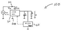
도 1은 본 발명을 구현하는 일반적인 원리에 따라 용량성 분배기를 사용하여조정되는 공급 전압을 발생시키기 위한 회로(100)를 도시하는 블록도이다. 도면 전체에 걸쳐, 동일한 부품을 지시하는 데에는 동일한 참조 번호가 사용되었다. 회로(100)는 노드(10a)에 가해지는 AC 전력 소스(10)를 포함한다. 전압 또는 전류 소스가 사용될 수 있는데, 주된 응용의 경우에 있어서 소스는, AC 전력 라인 입력을 포함하는 것으로 이해된다. 직렬로 연결된 커패시터(Cmains) 및 커패시터(CL)을 포함하는 용량성 분배기는, 노드(10a)에서의 입력 전압(Vin)을 부하 장치(RL) 양단에서 요구되는 출력 전압 레벨 V1으로 변환하기 위해 사용된다. 에너지 전달은 커패시터(Cmains)에 의해 결정되므로, 전압 소스는 자동으로 전류 소스로 간주될 수 있다.1 is a block diagram illustrating a
전압 분배기 배치(voltage divider arrangement)에 연결되어 있는 제어 회로(60)는 출력 전압 V1을 측정하고, 스위치형 정류기 회로(30)를 제어하기 위해 측정된 출력 전압과 기준 전압 Vref를 비교한다. 스위치형 정류기 회로(30)에 대해서는 두 개의 기본 배치가 있다. 제1 배치는, 요구되는 출력 전압 레벨에 도달하자마자(V1=Vref), 커패시터(CL)이 더 이상 충전되지 않도록 억제한다. 이 배치는 순방향 제어 션트 스위치(forward controlled shunt switch)로서 구현될 수 있다. 제2 배치는, 출력 전압(V1)이 요구되는 값(Vref)를 초과하는 동안에는, 커패시터 (CL)이 빠르게 방전되도록 한다. 이 배치는, 그 귀로 전류가 제어되는 제어형 직렬 스위치(controlled series switch)로서 구현될 수 있다. 이 두 개의 기본 구현들은 각각 도 2 및 도 3에 더 상세하게 도시되어 있다.The
예시 응용에서, 스위치 모드 전력 공급기 내에서 보조 전력의 생성은 다음의 방식으로 이루어질 수 있다. 이제, 도 2와 관련하여 주기 입력 전압 Vin의 소스는 정류기(12)에 연결된 AC 소스(10)로부터 노드(10a)로 진행되어 있다. 필터 커패시터(Cmains)의 제1 단자는 노드(10a)에 연결되어 있고, 제2 단자는 노드(10b)에 연결되어 있다. 다이오드(D1)은 노드(10b)와 접지(GND) 사이에 역-바이어스 형태로 연결되어 있다. 필터 커패시터(Cmains)는 다이오드(D2)를 통해서 커패시터(CL)과 연결되어 전압분배기 배치를 갖는다. 커패시터(CL)의 제1 단자는 노드(10c)에서 다이오드(D2)의 음극과 연결되어 있고, 제2 단자는 접지되어 있다. 스위치(S1)은 노드(10b)와 접지 사이에 다이오드(D1)과 병렬로 연결되어 있다. 제어 회로(60)는 노드(10c)에서 부하 저항(RL) 및 커패시터(CL)과 병렬로 연결되어 있다. 바이어스 저항(Rbias)는 노드(10a)와 노드(10c) 사이에 연결되어 있다. 다이오드(D2)가 순방향으로 바이어스된 경우(즉, 전도), 노드(10b)와 노드(10c)는 다이오드(D2) 양단의 상대적으로 소량의 전압 강하를 제외하면 실질적으로 동일한 전위인 것을 주목한다. 저항(Rbias)는 상대적으로 큰 값을 가져서, 일반적으로 사용되는 기본 제어기 IC에 대해 시동 전압(start up voltage)(V1)을 전달한다. 저항(Rmains)는 주요 부하 저항을 나타내며, 입력 노드(10a) 및 GND 사이에 연결되어 있다.In an example application, the generation of auxiliary power in a switch mode power supply can be made in the following manner. Referring now to FIG. 2, the source of the periodic input voltage Vin is advanced from
제어 회로(60)는, Cmains 및 CL을 선택적으로 연결하는 스위치(S1)에 통신으로 연결(대시 라인(63)으로 도시)되어 있다. 제어 회로(60)는 출력 전압(V1)을 감지하고, S1을 열거나 닫게 하는 제어 신호를 생성하기 위해 그 출력 전압과 미리 정해진 기준 전압 Vref를 비교하는데, 그럼으로써 Cmains와 CL 사이의 전기적 경로를 스위치로 연결/분리하게 된다. 노드(10c)에서의 출력 전압 V1은 기본 스위치 제어 회로 또는 제어기(60)를 위해 사용된다. 예시 구현에서, 스위치 제어 회로는 펄스 폭 변조(pulse width modulated, PWM) 제어 회로 또는 임의의 다른 유형의 스위치 제어 배치가 될 수 있다. 커패시터(Cmains)는 AC 신호를 스위치 정류 회로(30) 및 제어기(60)에 연결하는 것으로 이해된다.The
DC 전압 Vin은 나아가 주 부하 저항을 나타내는 Rmains 양단에 걸린다.The DC voltage Vin further goes across Rmains, which represents the main load resistance.
CL >> Cmains인 경우에, 커패시터(Cmains)는 본질적으로 노드(10a)에 걸리는 주기 입력 신호를 필터하기 위한 필터 커패시터로서 동작한다. CL 내에 전달된 에너지는 Cmains 내에 전달된 에너지보다 훨씬 더 적다. 스위치(S1)이 열렸을 때, 커패시터(CL)은 정류된 입력 전류(Iin)에 의해 전도 다이오드(D2)를 통해서 충전된다. 이는 충전 전류가 흐르는 동안에는, Cmains 및 CL 양단 전압의 증가로 나타난다. AC 소스(10)의 입력 전압이 전압 Vin 아래로 떨어지면, 정류기(12)는 AC 소스(10)를 회로의 나머지 부분(즉, 노드(10a))로부터 분리한다. 이 때, 커패시터(Cmains)는 전도 다이오드(D1)에 의해 전류를 부하(Rmains)로 전달한다. 이 경우, 다이오드(D2)는 그 사이에 흐르는 임의의 전류를 차단하는 역할을 하기 때문에 Cmains 및 CL 사이에 존재하는 전류 경로는 없다. CL을 통해 흐르는 상대적으로 소량의 전류는 부하 저항(RL)을 통해 방전된다. CL을 통해 흐르는 이 방전 전류는 오직 제어 회로(60) 및 부하(RL)에만 공급되고 있음을 주목한다. 이는, 예를 들면, 텔레비전 세트에서의 대기 전력(예를 들어 1-3 와트)을 나타낸다. 이는 다이오드(D1), 커패시터(Cmains) 및 TV 세트의 주 부하를 의미하는 Rmains(예를 들어 100-150 와트)를 통해 방전되는 전류의 양보다 훨씬 적은 것이다. 다이오드(D2)는 역 바이어스되기 때문에, CL 양단의 전압 V1은 양수로 유지되며, 전압 강하는 오직 보조 부하 저항(RL)에 의해서만 결정된다.In the case of CL >> Cmains, the capacitor Cmains essentially acts as a filter capacitor to filter the periodic input signal across
본 발명의 관점에 따라 Cmains의 충전 조건이 주로 CL 내에서 충전을 결정한다. 좀 더 구체적으로는 Cmains가 방전되는 제1 방전 주기 이후, 다음 주요 주기 동안에는 커패시터(Cmains)가 충전되며 동시에 다이오드(D2)의 전도에 기인하여 커패시터(CL)이 충전된다. 일 실시예에서, CL은 Cmains보다 대략 3-4배 더 큰 것(예컨대, Cmains는 약 68 uF(마이크로 패럿), 반면 CL은 220 uF)에 주목한다. Rmains 및 RL에서의 전압은 요구되는 출력 전압 V1을 얻기 위해 선택된 비율을 가짐을 주목한다. 그러나, 주 전력 공급기에 대한 Rmains는 종종 광범위하게 달라질 수 있다. 예를 들면, Rmains는 전형적으로 TV와 같은 소비자 전자 장치에 대한 주 전력 공급기이므로, 그 전력은 사운드, 영상 파라미터 등과 같은 요인들에 따라 50 W에서 150W의 범위에서 어떤 값이든 그 장치의 실행 모드 범위 내이면 될 수 있다. 그러나, V1의 대기 출력 전력은 1W 또는 그 미만으로 떨어질 수 있다. 나아가, 부하 RL은 예컨대, 마이크로프로세서, 제어기 및 IR 수신기와 같은 소형 신호 장치들에 공급하기 위해 실질적으로 상수로 유지된다.According to the aspect of the invention the charging conditions of the Cmains mainly determine the charging in CL. More specifically, after the first discharge period in which the Cmains are discharged, the capacitor Cmains is charged during the next main period and at the same time the capacitor CL is charged due to the conduction of the diode D2. In one embodiment, note that CL is approximately 3-4 times larger than Cmains (eg, Cmains is about 68 uF (microfarad), while CL is 220 uF). Note that the voltages at Rmains and RL have a selected ratio to obtain the required output voltage V1. However, the Rmains for the mains power supply can often vary widely. For example, Rmains is typically the main power supply for a consumer electronic device such as a TV, so that power can range from 50 W to 150 W, depending on factors such as sound, picture parameters, etc. It can be mine. However, the standby output power of V1 may drop to 1W or less. Further, the load RL remains substantially constant, for example for supplying small signal devices such as microprocessors, controllers and IR receivers.
도 2에 도시된 바와 같이, 스위치(S1)은 스위치형 션트 제어기 배치(shunt controller arrangement)로 구성되어 있다. 여기에서, S1은 제어 회로(60)의 신호에 응답하여 닫히며, 그럼으로써 노드 10c에서 요구되는 출력 전압에 도달되자마자 CL에 대한 더 이상의 충전은 억제된다. 이러한 방식으로, 스위치 S1을 열고 닫음으로써, RL 양단의 출력 전압 V1은 제어될 수 있다. 이 구현은 출력 전압이 미리 정해진 레벨을 넘어서면 안되는 경우, 회로 배치를 제공하는데 유용하다. 좀 더 구체적으로, CL에서 요구되는 출력 전압 레벨에 도달되어 제어 회로(60)에 의해 감지되자마자, CL에서 더 이상의 충전없이, 따라서 전압 V1으로 유지될 수 있도록 Cmains, S1 및 입력으로 돌아가는 전류 경로를 형성하기 위해 스위치(S1)은 닫힌다. S1은 50 또는 60Hz 입력 사인파의 1주기 내에서 닫히거나 열릴 수 있음을 주목한다.As shown in FIG. 2, the switch S1 is configured in a switched shunt controller arrangement. Here, S1 is closed in response to the signal of the
도 3에 다른 실시예가 도시되어 있다. 도 3의 실시예는 스위치(S1)이 노드(10b) 및 노드(10c) 사이에 전도 다이오드(D2)와 병렬로 연결되어 있다는 점에서 도 2와 다르다. 이 경우, 출력 전압 V1의 최대값은 임계 제한으로 정확하게 결정되지 않는다. 스위치(S1)은 제어 회로(60)의 신호에 응답하여, S1 및 Cmains를 통해서 CL로부터 Rmains까지 방전 경로를 활성화시키기 위해 닫힌다. 요구되는 출력 전압의 최소값에 도달되자마자 스위치가 열리면, 더 이상의 Rmains로의 방전은 억제된다. 이 구현에서, RL 양단의 출력 전압은 충전 주기(S1이 열린 경우) 동안 제어되지 않는다. 상술된 실시예는 직렬 연결된 레귤레이터와 같은 전압 제한기 뒤에 오는 경우에는 언제나 유용한 해결책을 제시한다. 도 3에 따른 해결은, 유용하 게도 Cmains 및 라인 정류기 내에서 과도 전류(current transients)를 생성하지 않는다. 도 2 및 도 3에 도시된 상술된 실시예로부터, 도 2의 실시예에서는 충전이 제어되고, 반면 도 3의 실시예에서는 방전이 제어된다.Another embodiment is shown in FIG. 3. The embodiment of FIG. 3 differs from FIG. 2 in that the switch S1 is connected in parallel with the conducting diode D2 between the node 10b and the node 10c. In this case, the maximum value of the output voltage V1 is not accurately determined by the threshold limit. The switch S1 is closed in response to the signal of the
도 2 및 도 3의 방식 개념을 구현하는 세부 회로도가 각각 도 4 및 도 5에 도시되어 있다. 도시된 대로, 스위치 모드 전력 공급기에서 일반적으로 사용되는 기본 제어기에 대해 보조 전력을 생성하기 위한 배치가 구현되어 있다. 초기 시동 전압은 Rbias에 의해 제공된다. 정상 실행 모드에서, 제어기에 대한 전력 소모는 저항(Rbias)이 전달할 수 있는 것보다 더 높다. 여기에서, 이용되는 커패시터 (Cmains 및 CL)는 상술된 바와 같이 제어기에 전력을 지원한다. 도 2의 개념적인 스위치(S1)는, 도 4에서 고이득 트랜지스터(Q1 및 Q2)라는 수단으로 성립되어 있다. 도 4에 도시된 대로, pnp 트랜지스터(Q1)은 그의 베이스 단자(b1)가 트랜지스터(Q2)의 c2 단자에 연결되어 있다. Q1의 e1 단자는 노드(10b)에 연결되어 있으며, 반면, Q1의 c1 단자는 npn 트랜지스터(Q2)의 베이스 단자(b2)에 연결되어 있다. c1, b2 단자는 노드(10d)에 연결되어 있으며, 노드(10d)는 저항(R2)을 통해 GND에 연결되어 있다. 저항(R1)은 Q1, Q2의 b1, c2 단자를 각각 노드(10b)에 연결한다. 제너 다이오드(Zener diode)(D4)는 노드(10c)와 노드(10d) 사이에 연결되어 있다. 출력 전압은 다이오드(D4)에 의해 감지되며, 고이득 트랜지스터(Q1, Q2)를 직접 제어한다. 회로(400)는 실행 전력이 없는 발진기에서 구현될 수 있는데, 이 때 발진기의 동작은 2차 사이드(410)의 출력 전압에 따라 활성화/억제된다. 앞서 언급된 대로, 초기 시동 전압은 Rbias에 의해 공급된다. CL 양단의 전압이 임계값 아래인 동안, D2를 통해 Cmains로부터 CL로 향하는 전류 경로가 성립되며, 커패시터(Cmains 및 CL)는 충전을 계속한다. 그러나, 전력 발진기의 동작에 따라 발진기에서 소모되는 전력은 Rbias가 전달할 수 있는 것 보다 더 높다. 그러므로, Cmains 및 CL에 저장된 에너지가 전력 발진기의 구동기에 전력을 공급하기 위해 사용된다.Detailed circuit diagrams for implementing the scheme concept of FIGS. 2 and 3 are shown in FIGS. 4 and 5, respectively. As shown, arrangements for generating auxiliary power for primary controllers commonly used in switch mode power supplies are implemented. The initial starting voltage is provided by Rbias. In normal run mode, the power consumption for the controller is higher than the resistance Rbias can deliver. Here, the capacitors Cmains and CL used support power to the controller as described above. The conceptual switch S1 of FIG. 2 is established by means of high gain transistors Q1 and Q2 in FIG. As shown in FIG. 4, the pnp transistor Q1 has its base terminal b1 connected to the c2 terminal of the transistor Q2. The e1 terminal of Q1 is connected to the node 10b, while the c1 terminal of Q1 is connected to the base terminal b2 of the npn transistor Q2. The c1 and b2 terminals are connected to the node 10d, and the node 10d is connected to the GND through the resistor R2. The resistor R1 connects the b1 and c2 terminals of Q1 and Q2 to the node 10b, respectively. Zener diode D4 is connected between node 10c and node 10d. The output voltage is sensed by the diode D4 and directly controls the high gain transistors Q1 and Q2. The
유사한 방식으로 도 3의 스위치(S1)는 도 5에 도시된 회로 배치(500)에서는 트랜지스터(Q1)으로서 구현되어 있다. 도 5에 도시된 대로, pnp 트랜지스터(Q1)은 그의 베이스 단자(b1)가 저항(R2)을 통해서 npn 트랜지스터(Q2)의 c2 단자에 연결되어 있다. Q1의 e1 단자는 다이오드(D2)의 음극에 연결되어 있으며, 반면, Q1의 c1 단자는 노드(10b)에서 다이오드(D2)의 양극에 연결되어 있다. 저항(R1)은, R2와의 전압 분배기 배치 내에서 D2의 음극과 Q1의 b1 단자 사이에 연결되어 있다. 다이오드(D1)는 노드(10b)와 GND 사이에 연결되어 있다. npn 트랜지스터(Q2)의 베이스 단자(b2)는 노드(10e)에서 제너 다이오드(D4)와 연결되어 있다. 저항(R3)는 노드(10e)와 GND 사이에 연결되어 있으며, 반면 다이오드(D4)의 음극은 저항(R4)를 통해서 노드(10c)에 연결되어 있다. 트랜지스터(Q2)의 e2단자는 GND에 연결되어 있다. 여기에서, 제너 다이오드(D4)는 제어기(60)의 입력에서 구동 전압을 주어진 또는 미리 정해진 값으로 제한한다. 다이오드(D4)는 드라이버(Q2)를 통해서 Q1을 제어한다. 그러므로, 커패시터(CL)은 제어기(60)의 입력에서 요구되는 최소 전압에 도달될 때까지 Cmains에 또, 2차 사이드 상에 변환된 부하(Rs)에 대응하는 주 부하(Rmains)에 스위치로 연결되어 있는 상태가 유지된다. 그 때, 커패시터(CL)은 제어기에 요구되는 상대적으로 작은 전류로써 제어 회로(60)를 통해 방전된다. 이것은 Cmains에 다음 충전 기간이 도달할 때까지 발생한다. 대안적인 배치로서, 다이오드(D4)는 일반적으로 사용되는 직렬 전압 제한기 또는 안정화 회로의 일부일 수 있다.In a similar manner, the switch S1 of FIG. 3 is implemented as the transistor Q1 in the
비록 본 발명이 예시 실시예에 관하여 설명되었지만, 그에 한정되지 않는다. 첨부된 청구항들은, 본 발명의 균등 범위와 사상을 벗어나지 않고 당업자에 의해 이루어질 수 있는 실시예들 및 다른 변형들을 포함하는 것으로 폭넓게 해석되어야 한다.Although the present invention has been described with reference to exemplary embodiments, it is not limited thereto. The appended claims should be construed broadly to include embodiments and other modifications that can be made by those skilled in the art without departing from the scope and spirit of the present invention.
Claims (19)
Translated fromKoreanApplications Claiming Priority (3)
| Application Number | Priority Date | Filing Date | Title |
|---|---|---|---|
| US41882302P | 2002-10-16 | 2002-10-16 | |
| US60/418,823 | 2002-10-16 | ||
| PCT/IB2003/005308WO2004038902A2 (en) | 2002-10-16 | 2003-10-16 | Capacitively coupled power supply |
Publications (2)
| Publication Number | Publication Date |
|---|---|
| KR20050048691A KR20050048691A (en) | 2005-05-24 |
| KR101084411B1true KR101084411B1 (en) | 2011-11-21 |
Family
ID=32107978
Family Applications (1)
| Application Number | Title | Priority Date | Filing Date |
|---|---|---|---|
| KR1020057006633AExpired - Fee RelatedKR101084411B1 (en) | 2002-10-16 | 2003-10-16 | Capacitively Coupled Power Supplies |
Country Status (10)
| Country | Link |
|---|---|
| US (1) | US7019992B1 (en) |
| EP (1) | EP1552596B1 (en) |
| JP (1) | JP4457014B2 (en) |
| KR (1) | KR101084411B1 (en) |
| CN (1) | CN1703825B (en) |
| AU (1) | AU2003276632A1 (en) |
| DE (1) | DE60326616D1 (en) |
| MX (1) | MXPA05004085A (en) |
| MY (2) | MY134548A (en) |
| WO (1) | WO2004038902A2 (en) |
Families Citing this family (19)
| Publication number | Priority date | Publication date | Assignee | Title |
|---|---|---|---|---|
| FR2876515A1 (en)* | 2004-10-08 | 2006-04-14 | St Microelectronics Sa | DOUBLE POWER SUPPLY CIRCUIT |
| US8213197B1 (en)* | 2006-09-05 | 2012-07-03 | Marvell International Ltd. | Switching capacitor power supply |
| US8619443B2 (en) | 2010-09-29 | 2013-12-31 | The Powerwise Group, Inc. | System and method to boost voltage |
| US20110182094A1 (en)* | 2007-08-13 | 2011-07-28 | The Powerwise Group, Inc. | System and method to manage power usage |
| US8085009B2 (en) | 2007-08-13 | 2011-12-27 | The Powerwise Group, Inc. | IGBT/FET-based energy savings device for reducing a predetermined amount of voltage using pulse width modulation |
| US8085010B2 (en) | 2007-08-24 | 2011-12-27 | The Powerwise Group, Inc. | TRIAC/SCR-based energy savings device for reducing a predetermined amount of voltage using pulse width modulation |
| US8120307B2 (en)* | 2007-08-24 | 2012-02-21 | The Powerwise Group, Inc. | System and method for providing constant loading in AC power applications |
| US8810190B2 (en)* | 2007-09-14 | 2014-08-19 | The Powerwise Group, Inc. | Motor controller system and method for maximizing energy savings |
| US8698447B2 (en) | 2007-09-14 | 2014-04-15 | The Powerwise Group, Inc. | Energy saving system and method for devices with rotating or reciprocating masses |
| JP5400131B2 (en)* | 2008-03-25 | 2014-01-29 | トムソン ライセンシング | Snubber capacitor for generating auxiliary power supply voltage |
| US8004255B2 (en)* | 2008-08-07 | 2011-08-23 | The Powerwise Group, Inc. | Power supply for IGBT/FET drivers |
| US8698446B2 (en)* | 2009-09-08 | 2014-04-15 | The Powerwise Group, Inc. | Method to save energy for devices with rotating or reciprocating masses |
| MX2012003008A (en) | 2009-09-08 | 2012-04-19 | Powerwise Group Inc | Energy saving system and method for devices with rotating or reciprocating masses. |
| DE112011100734A5 (en)* | 2010-03-02 | 2013-09-26 | Em Microelectronic-Marin S.A. | Electrical device with a suppression capacitor circuit |
| US8830637B2 (en)* | 2010-08-31 | 2014-09-09 | Texas Instruments Incorporated | Methods and apparatus to clamp overvoltages for alternating current systems |
| TW201328152A (en)* | 2011-12-28 | 2013-07-01 | Ushijima Masakazu | Auxiliary power supply generation circuit |
| CN104272577B (en)* | 2012-03-02 | 2017-06-30 | 施耐德电气It公司 | The method and electric power system of low voltage DC power are provided from AC feeder cables |
| JP6298994B1 (en)* | 2017-09-14 | 2018-03-28 | パナソニックIpマネジメント株式会社 | Power supply circuit and motor drive device |
| US20230231489A1 (en)* | 2022-01-14 | 2023-07-20 | Ut-Battelle, Llc | System for bulk capacitance reduction |
Citations (2)
| Publication number | Priority date | Publication date | Assignee | Title |
|---|---|---|---|---|
| US4801887A (en) | 1986-04-10 | 1989-01-31 | U.S. Philips Corp. | Circuit arrangement for generating a direct voltage from a sinusoidal input voltage |
| US6046916A (en) | 1996-07-26 | 2000-04-04 | Sgs-Thomson Microelectronics S.A. | High and low d.c. voltage power supply |
Family Cites Families (12)
| Publication number | Priority date | Publication date | Assignee | Title |
|---|---|---|---|---|
| US3497792A (en)* | 1967-11-20 | 1970-02-24 | Westinghouse Electric Corp | High voltage to low voltage inverters |
| DE2836325A1 (en)* | 1978-08-19 | 1980-02-28 | Bosch Gmbh Robert | AC=DC smoothing and rectification circuit - has smoothing capacitor connected to decoupling capacitor to derive AC low voltage supply from ripple in rectified DC supply |
| US4578772A (en)* | 1981-09-18 | 1986-03-25 | Fujitsu Limited | Voltage dividing circuit |
| US4649468A (en)* | 1985-11-06 | 1987-03-10 | At&T Information Systems Inc. | Voltage divider circuit |
| EP0297545B1 (en)* | 1987-07-01 | 1992-04-22 | Hitachi, Ltd. | Power supply circuit |
| JP2938958B2 (en)* | 1990-10-31 | 1999-08-25 | 富士通株式会社 | DC-DC converter |
| DE4040841A1 (en)* | 1990-12-20 | 1992-06-25 | Philips Patentverwaltung | Circuit producing DC feed voltage for at least one load - delivers DC voltage essentially between two terminals with at least one user fed across converter system contg. inductance and switch in series |
| US5596489A (en)* | 1994-01-14 | 1997-01-21 | Intel Corporation | Capacitive transformer having a switch responsive to clock signals |
| IT1291466B1 (en)* | 1997-01-24 | 1999-01-11 | Bitron Spa | AC-DC CONVERTER FOR LOW POWER, MAINS POWERED, HIGH EFFICIENCY AND SELF-PROTECTED ELECTRONIC COMMUTATION MOTORS. |
| EP1174998B1 (en)* | 2000-06-21 | 2003-05-14 | MAGNETEK S.p.A. | Brushless motor,method and circuit for its control |
| JP2003111386A (en)* | 2001-09-26 | 2003-04-11 | Sanyo Electric Co Ltd | Method of controlling dc-dc converter |
| JP4137528B2 (en)* | 2002-06-13 | 2008-08-20 | セイコーインスツル株式会社 | Power conversion circuit |
- 2003
- 2003-10-15MYMYPI20033933Apatent/MY134548A/enunknown
- 2003-10-15MYMYPI20033932Apatent/MY134537A/enunknown
- 2003-10-16DEDE60326616Tpatent/DE60326616D1/ennot_activeExpired - Lifetime
- 2003-10-16CNCN2003801013136Apatent/CN1703825B/ennot_activeExpired - Fee Related
- 2003-10-16MXMXPA05004085Apatent/MXPA05004085A/enactiveIP Right Grant
- 2003-10-16EPEP03809408Apatent/EP1552596B1/ennot_activeExpired - Lifetime
- 2003-10-16USUS10/531,118patent/US7019992B1/ennot_activeExpired - Lifetime
- 2003-10-16AUAU2003276632Apatent/AU2003276632A1/ennot_activeAbandoned
- 2003-10-16KRKR1020057006633Apatent/KR101084411B1/ennot_activeExpired - Fee Related
- 2003-10-16JPJP2004546312Apatent/JP4457014B2/ennot_activeExpired - Fee Related
- 2003-10-16WOPCT/IB2003/005308patent/WO2004038902A2/enactiveApplication Filing
Patent Citations (2)
| Publication number | Priority date | Publication date | Assignee | Title |
|---|---|---|---|---|
| US4801887A (en) | 1986-04-10 | 1989-01-31 | U.S. Philips Corp. | Circuit arrangement for generating a direct voltage from a sinusoidal input voltage |
| US6046916A (en) | 1996-07-26 | 2000-04-04 | Sgs-Thomson Microelectronics S.A. | High and low d.c. voltage power supply |
Also Published As
| Publication number | Publication date |
|---|---|
| MXPA05004085A (en) | 2005-06-08 |
| US20060067094A1 (en) | 2006-03-30 |
| CN1703825A (en) | 2005-11-30 |
| WO2004038902A3 (en) | 2004-07-22 |
| MY134548A (en) | 2007-12-31 |
| MY134537A (en) | 2007-12-31 |
| WO2004038902A2 (en) | 2004-05-06 |
| US7019992B1 (en) | 2006-03-28 |
| JP4457014B2 (en) | 2010-04-28 |
| AU2003276632A8 (en) | 2004-05-13 |
| EP1552596A2 (en) | 2005-07-13 |
| EP1552596B1 (en) | 2009-03-11 |
| CN1703825B (en) | 2012-07-04 |
| DE60326616D1 (en) | 2009-04-23 |
| AU2003276632A1 (en) | 2004-05-13 |
| KR20050048691A (en) | 2005-05-24 |
| JP2006511182A (en) | 2006-03-30 |
Similar Documents
| Publication | Publication Date | Title |
|---|---|---|
| KR101084411B1 (en) | Capacitively Coupled Power Supplies | |
| KR100411326B1 (en) | A low power dissipation power supply and controller | |
| US5691889A (en) | Controller having feed-forward and synchronization features | |
| JP4972112B2 (en) | Method and apparatus for switched mode power supplies that generate high pulse width modulation while maintaining low noise sensitivity | |
| KR100625598B1 (en) | Switching power supply apparatus | |
| JP4416510B2 (en) | Method and apparatus for maintaining a constant load current in a switch mode power supply | |
| KR101365100B1 (en) | Low power consumption start-up circuit with dynamic switching | |
| US6879501B2 (en) | Switching power supply | |
| TWI414142B (en) | Power supply control method and system therefor | |
| WO2000036739A1 (en) | Power converter circuit and method for controlling | |
| KR20040037584A (en) | Pulse width modulation signal generator and switching mode power supply including the same | |
| US6246596B1 (en) | Switching power supply | |
| KR101091923B1 (en) | Switching mode power supply and method for producing bias voltage thereof | |
| JPH1014127A (en) | Multifunctional battery charger self-aligns as a supply voltage regulator for battery powered devices | |
| CN100449922C (en) | Start-up circuit for power supply | |
| US6369552B2 (en) | Regulated auxiliary power supply | |
| US6587357B1 (en) | Method and apparatus for providing integrated low power self-supply in switched mode power supplies | |
| US11146172B2 (en) | Startup/brownout active clamping for capacitor-drop power supply | |
| JP2004274885A (en) | Switching power supply | |
| KR102049965B1 (en) | Rectifying apparatus having stand-by power saving function | |
| JP2004222472A (en) | Switching power supply control circuit | |
| US6233164B1 (en) | Protection circuit for a switched-mode power supply | |
| JPH04217861A (en) | Switching power supply | |
| KR100286044B1 (en) | Monitoring Circuit for Output Status of Switched-Mode Power Supplies | |
| JP4690213B2 (en) | DC / DC converter |
Legal Events
| Date | Code | Title | Description |
|---|---|---|---|
| PA0105 | International application | St.27 status event code:A-0-1-A10-A15-nap-PA0105 | |
| E13-X000 | Pre-grant limitation requested | St.27 status event code:A-2-3-E10-E13-lim-X000 | |
| P11-X000 | Amendment of application requested | St.27 status event code:A-2-2-P10-P11-nap-X000 | |
| P13-X000 | Application amended | St.27 status event code:A-2-2-P10-P13-nap-X000 | |
| PG1501 | Laying open of application | St.27 status event code:A-1-1-Q10-Q12-nap-PG1501 | |
| PN2301 | Change of applicant | St.27 status event code:A-3-3-R10-R13-asn-PN2301 St.27 status event code:A-3-3-R10-R11-asn-PN2301 | |
| P22-X000 | Classification modified | St.27 status event code:A-2-2-P10-P22-nap-X000 | |
| A201 | Request for examination | ||
| P11-X000 | Amendment of application requested | St.27 status event code:A-2-2-P10-P11-nap-X000 | |
| P13-X000 | Application amended | St.27 status event code:A-2-2-P10-P13-nap-X000 | |
| PA0201 | Request for examination | St.27 status event code:A-1-2-D10-D11-exm-PA0201 | |
| E902 | Notification of reason for refusal | ||
| PE0902 | Notice of grounds for rejection | St.27 status event code:A-1-2-D10-D21-exm-PE0902 | |
| T11-X000 | Administrative time limit extension requested | St.27 status event code:U-3-3-T10-T11-oth-X000 | |
| T11-X000 | Administrative time limit extension requested | St.27 status event code:U-3-3-T10-T11-oth-X000 | |
| T11-X000 | Administrative time limit extension requested | St.27 status event code:U-3-3-T10-T11-oth-X000 | |
| T11-X000 | Administrative time limit extension requested | St.27 status event code:U-3-3-T10-T11-oth-X000 | |
| E13-X000 | Pre-grant limitation requested | St.27 status event code:A-2-3-E10-E13-lim-X000 | |
| P11-X000 | Amendment of application requested | St.27 status event code:A-2-2-P10-P11-nap-X000 | |
| P13-X000 | Application amended | St.27 status event code:A-2-2-P10-P13-nap-X000 | |
| E701 | Decision to grant or registration of patent right | ||
| PE0701 | Decision of registration | St.27 status event code:A-1-2-D10-D22-exm-PE0701 | |
| R18-X000 | Changes to party contact information recorded | St.27 status event code:A-3-3-R10-R18-oth-X000 | |
| GRNT | Written decision to grant | ||
| PR0701 | Registration of establishment | St.27 status event code:A-2-4-F10-F11-exm-PR0701 | |
| PR1002 | Payment of registration fee | St.27 status event code:A-2-2-U10-U12-oth-PR1002 Fee payment year number:1 | |
| PG1601 | Publication of registration | St.27 status event code:A-4-4-Q10-Q13-nap-PG1601 | |
| FPAY | Annual fee payment | Payment date:20141023 Year of fee payment:4 | |
| PR1001 | Payment of annual fee | St.27 status event code:A-4-4-U10-U11-oth-PR1001 Fee payment year number:4 | |
| FPAY | Annual fee payment | Payment date:20151016 Year of fee payment:5 | |
| PR1001 | Payment of annual fee | St.27 status event code:A-4-4-U10-U11-oth-PR1001 Fee payment year number:5 | |
| FPAY | Annual fee payment | Payment date:20161019 Year of fee payment:6 | |
| PR1001 | Payment of annual fee | St.27 status event code:A-4-4-U10-U11-oth-PR1001 Fee payment year number:6 | |
| FPAY | Annual fee payment | Payment date:20171018 Year of fee payment:7 | |
| PR1001 | Payment of annual fee | St.27 status event code:A-4-4-U10-U11-oth-PR1001 Fee payment year number:7 | |
| R17-X000 | Change to representative recorded | St.27 status event code:A-5-5-R10-R17-oth-X000 | |
| FPAY | Annual fee payment | Payment date:20181031 Year of fee payment:8 | |
| PR1001 | Payment of annual fee | St.27 status event code:A-4-4-U10-U11-oth-PR1001 Fee payment year number:8 | |
| R18-X000 | Changes to party contact information recorded | St.27 status event code:A-5-5-R10-R18-oth-X000 | |
| PN2301 | Change of applicant | St.27 status event code:A-5-5-R10-R11-asn-PN2301 | |
| PN2301 | Change of applicant | St.27 status event code:A-5-5-R10-R14-asn-PN2301 | |
| PN2301 | Change of applicant | St.27 status event code:A-5-5-R10-R11-asn-PN2301 | |
| PN2301 | Change of applicant | St.27 status event code:A-5-5-R10-R14-asn-PN2301 | |
| FPAY | Annual fee payment | Payment date:20191030 Year of fee payment:9 | |
| PR1001 | Payment of annual fee | St.27 status event code:A-4-4-U10-U11-oth-PR1001 Fee payment year number:9 | |
| PC1903 | Unpaid annual fee | St.27 status event code:A-4-4-U10-U13-oth-PC1903 Not in force date:20201111 Payment event data comment text:Termination Category : DEFAULT_OF_REGISTRATION_FEE | |
| PN2301 | Change of applicant | St.27 status event code:A-5-5-R10-R13-asn-PN2301 St.27 status event code:A-5-5-R10-R11-asn-PN2301 | |
| PC1903 | Unpaid annual fee | St.27 status event code:N-4-6-H10-H13-oth-PC1903 Ip right cessation event data comment text:Termination Category : DEFAULT_OF_REGISTRATION_FEE Not in force date:20201111 | |
| P22-X000 | Classification modified | St.27 status event code:A-4-4-P10-P22-nap-X000 |