KR101082254B1 - Organic light emitting display device and method of manufacturing the same - Google Patents
Organic light emitting display device and method of manufacturing the sameDownload PDFInfo
- Publication number
- KR101082254B1 KR101082254B1KR1020090105986AKR20090105986AKR101082254B1KR 101082254 B1KR101082254 B1KR 101082254B1KR 1020090105986 AKR1020090105986 AKR 1020090105986AKR 20090105986 AKR20090105986 AKR 20090105986AKR 101082254 B1KR101082254 B1KR 101082254B1
- Authority
- KR
- South Korea
- Prior art keywords
- electrode
- insulating layer
- layer
- anode
- light emitting
- Prior art date
- Legal status (The legal status is an assumption and is not a legal conclusion. Google has not performed a legal analysis and makes no representation as to the accuracy of the status listed.)
- Active
Links
- 238000004519manufacturing processMethods0.000titleclaimsabstractdescription15
- 239000004065semiconductorSubstances0.000claimsabstractdescription27
- 239000011368organic materialSubstances0.000claimsabstractdescription12
- 238000000034methodMethods0.000claimsdescription21
- 239000000758substrateSubstances0.000claimsdescription9
- XLOMVQKBTHCTTD-UHFFFAOYSA-NZinc monoxideChemical compound[Zn]=OXLOMVQKBTHCTTD-UHFFFAOYSA-N0.000claimsdescription7
- 238000000059patterningMethods0.000claimsdescription5
- GYHNNYVSQQEPJS-UHFFFAOYSA-NGalliumChemical compound[Ga]GYHNNYVSQQEPJS-UHFFFAOYSA-N0.000claimsdescription3
- NIXOWILDQLNWCW-UHFFFAOYSA-Nacrylic acid groupChemical groupC(C=C)(=O)ONIXOWILDQLNWCW-UHFFFAOYSA-N0.000claimsdescription3
- 238000004140cleaningMethods0.000claimsdescription3
- 229910052733galliumInorganic materials0.000claimsdescription3
- 229910052738indiumInorganic materials0.000claimsdescription3
- APFVFJFRJDLVQX-UHFFFAOYSA-Nindium atomChemical compound[In]APFVFJFRJDLVQX-UHFFFAOYSA-N0.000claimsdescription3
- 229920001721polyimidePolymers0.000claimsdescription3
- 239000004642PolyimideSubstances0.000claimsdescription2
- 229910052735hafniumInorganic materials0.000claimsdescription2
- VBJZVLUMGGDVMO-UHFFFAOYSA-Nhafnium atomChemical compound[Hf]VBJZVLUMGGDVMO-UHFFFAOYSA-N0.000claimsdescription2
- 238000005406washingMethods0.000claimsdescription2
- XLYOFNOQVPJJNP-UHFFFAOYSA-NwaterSubstancesOXLYOFNOQVPJJNP-UHFFFAOYSA-N0.000claimsdescription2
- 239000010409thin filmSubstances0.000abstractdescription14
- 229910052739hydrogenInorganic materials0.000abstractdescription8
- 239000001257hydrogenSubstances0.000abstractdescription8
- 238000009792diffusion processMethods0.000abstractdescription2
- 125000004435hydrogen atomChemical class[H]*0.000abstract1
- 229910052751metalInorganic materials0.000description8
- 239000002184metalSubstances0.000description8
- 239000010936titaniumSubstances0.000description5
- UFHFLCQGNIYNRP-UHFFFAOYSA-NHydrogenChemical compound[H][H]UFHFLCQGNIYNRP-UHFFFAOYSA-N0.000description4
- 239000011651chromiumSubstances0.000description4
- 239000010949copperSubstances0.000description4
- 239000010931goldSubstances0.000description4
- 238000010438heat treatmentMethods0.000description4
- 239000010955niobiumSubstances0.000description4
- 229910021420polycrystalline siliconInorganic materials0.000description4
- RTAQQCXQSZGOHL-UHFFFAOYSA-NTitaniumChemical compound[Ti]RTAQQCXQSZGOHL-UHFFFAOYSA-N0.000description3
- 150000002431hydrogenChemical class0.000description3
- 229910052719titaniumInorganic materials0.000description3
- VYZAMTAEIAYCRO-UHFFFAOYSA-NChromiumChemical compound[Cr]VYZAMTAEIAYCRO-UHFFFAOYSA-N0.000description2
- RYGMFSIKBFXOCR-UHFFFAOYSA-NCopperChemical compound[Cu]RYGMFSIKBFXOCR-UHFFFAOYSA-N0.000description2
- 229910005265GaInZnOInorganic materials0.000description2
- ZOKXTWBITQBERF-UHFFFAOYSA-NMolybdenumChemical compound[Mo]ZOKXTWBITQBERF-UHFFFAOYSA-N0.000description2
- BQCADISMDOOEFD-UHFFFAOYSA-NSilverChemical compound[Ag]BQCADISMDOOEFD-UHFFFAOYSA-N0.000description2
- 229910045601alloyInorganic materials0.000description2
- 239000000956alloySubstances0.000description2
- 229910052782aluminiumInorganic materials0.000description2
- XAGFODPZIPBFFR-UHFFFAOYSA-NaluminiumChemical compound[Al]XAGFODPZIPBFFR-UHFFFAOYSA-N0.000description2
- 229910021417amorphous siliconInorganic materials0.000description2
- 229910052804chromiumInorganic materials0.000description2
- 229910052802copperInorganic materials0.000description2
- PCHJSUWPFVWCPO-UHFFFAOYSA-NgoldChemical compound[Au]PCHJSUWPFVWCPO-UHFFFAOYSA-N0.000description2
- 229910052737goldInorganic materials0.000description2
- 150000002739metalsChemical class0.000description2
- 229910052750molybdenumInorganic materials0.000description2
- 239000011733molybdenumSubstances0.000description2
- 229910052758niobiumInorganic materials0.000description2
- GUCVJGMIXFAOAE-UHFFFAOYSA-Nniobium atomChemical compound[Nb]GUCVJGMIXFAOAE-UHFFFAOYSA-N0.000description2
- 229920005591polysiliconPolymers0.000description2
- 229910052709silverInorganic materials0.000description2
- 239000004332silverSubstances0.000description2
- 229910052715tantalumInorganic materials0.000description2
- GUVRBAGPIYLISA-UHFFFAOYSA-Ntantalum atomChemical compound[Ta]GUVRBAGPIYLISA-UHFFFAOYSA-N0.000description2
- WFKWXMTUELFFGS-UHFFFAOYSA-NtungstenChemical compound[W]WFKWXMTUELFFGS-UHFFFAOYSA-N0.000description2
- 229910052721tungstenInorganic materials0.000description2
- 239000010937tungstenSubstances0.000description2
- 239000006227byproductSubstances0.000description1
- 239000011248coating agentSubstances0.000description1
- 238000000576coating methodMethods0.000description1
- 239000000356contaminantSubstances0.000description1
- 238000007796conventional methodMethods0.000description1
- 238000001312dry etchingMethods0.000description1
- 238000005530etchingMethods0.000description1
- 239000011521glassSubstances0.000description1
- AMGQUBHHOARCQH-UHFFFAOYSA-Nindium;oxotinChemical compound[In].[Sn]=OAMGQUBHHOARCQH-UHFFFAOYSA-N0.000description1
- 238000009413insulationMethods0.000description1
- 238000005468ion implantationMethods0.000description1
- 238000012986modificationMethods0.000description1
- 230000004048modificationEffects0.000description1
- 230000035515penetrationEffects0.000description1
- 239000004033plasticSubstances0.000description1
- 238000011160researchMethods0.000description1
- YVTHLONGBIQYBO-UHFFFAOYSA-Nzinc indium(3+) oxygen(2-)Chemical compound[O--].[Zn++].[In+3]YVTHLONGBIQYBO-UHFFFAOYSA-N0.000description1
Images


Classifications
- H—ELECTRICITY
- H10—SEMICONDUCTOR DEVICES; ELECTRIC SOLID-STATE DEVICES NOT OTHERWISE PROVIDED FOR
- H10K—ORGANIC ELECTRIC SOLID-STATE DEVICES
- H10K59/00—Integrated devices, or assemblies of multiple devices, comprising at least one organic light-emitting element covered by group H10K50/00
- H10K59/10—OLED displays
- H10K59/12—Active-matrix OLED [AMOLED] displays
- H10K59/124—Insulating layers formed between TFT elements and OLED elements
- H—ELECTRICITY
- H10—SEMICONDUCTOR DEVICES; ELECTRIC SOLID-STATE DEVICES NOT OTHERWISE PROVIDED FOR
- H10D—INORGANIC ELECTRIC SEMICONDUCTOR DEVICES
- H10D86/00—Integrated devices formed in or on insulating or conducting substrates, e.g. formed in silicon-on-insulator [SOI] substrates or on stainless steel or glass substrates
- H10D86/40—Integrated devices formed in or on insulating or conducting substrates, e.g. formed in silicon-on-insulator [SOI] substrates or on stainless steel or glass substrates characterised by multiple TFTs
- H10D86/421—Integrated devices formed in or on insulating or conducting substrates, e.g. formed in silicon-on-insulator [SOI] substrates or on stainless steel or glass substrates characterised by multiple TFTs having a particular composition, shape or crystalline structure of the active layer
- H10D86/423—Integrated devices formed in or on insulating or conducting substrates, e.g. formed in silicon-on-insulator [SOI] substrates or on stainless steel or glass substrates characterised by multiple TFTs having a particular composition, shape or crystalline structure of the active layer comprising semiconductor materials not belonging to the Group IV, e.g. InGaZnO
- H—ELECTRICITY
- H10—SEMICONDUCTOR DEVICES; ELECTRIC SOLID-STATE DEVICES NOT OTHERWISE PROVIDED FOR
- H10D—INORGANIC ELECTRIC SEMICONDUCTOR DEVICES
- H10D86/00—Integrated devices formed in or on insulating or conducting substrates, e.g. formed in silicon-on-insulator [SOI] substrates or on stainless steel or glass substrates
- H10D86/40—Integrated devices formed in or on insulating or conducting substrates, e.g. formed in silicon-on-insulator [SOI] substrates or on stainless steel or glass substrates characterised by multiple TFTs
- H10D86/451—Integrated devices formed in or on insulating or conducting substrates, e.g. formed in silicon-on-insulator [SOI] substrates or on stainless steel or glass substrates characterised by multiple TFTs characterised by the compositions or shapes of the interlayer dielectrics
- H—ELECTRICITY
- H10—SEMICONDUCTOR DEVICES; ELECTRIC SOLID-STATE DEVICES NOT OTHERWISE PROVIDED FOR
- H10D—INORGANIC ELECTRIC SEMICONDUCTOR DEVICES
- H10D86/00—Integrated devices formed in or on insulating or conducting substrates, e.g. formed in silicon-on-insulator [SOI] substrates or on stainless steel or glass substrates
- H10D86/40—Integrated devices formed in or on insulating or conducting substrates, e.g. formed in silicon-on-insulator [SOI] substrates or on stainless steel or glass substrates characterised by multiple TFTs
- H10D86/60—Integrated devices formed in or on insulating or conducting substrates, e.g. formed in silicon-on-insulator [SOI] substrates or on stainless steel or glass substrates characterised by multiple TFTs wherein the TFTs are in active matrices
- H—ELECTRICITY
- H10—SEMICONDUCTOR DEVICES; ELECTRIC SOLID-STATE DEVICES NOT OTHERWISE PROVIDED FOR
- H10K—ORGANIC ELECTRIC SOLID-STATE DEVICES
- H10K59/00—Integrated devices, or assemblies of multiple devices, comprising at least one organic light-emitting element covered by group H10K50/00
- H10K59/10—OLED displays
- H10K59/12—Active-matrix OLED [AMOLED] displays
- H10K59/121—Active-matrix OLED [AMOLED] displays characterised by the geometry or disposition of pixel elements
- H10K59/1213—Active-matrix OLED [AMOLED] displays characterised by the geometry or disposition of pixel elements the pixel elements being TFTs
Landscapes
- Engineering & Computer Science (AREA)
- Microelectronics & Electronic Packaging (AREA)
- Physics & Mathematics (AREA)
- Geometry (AREA)
- Electroluminescent Light Sources (AREA)
- Thin Film Transistor (AREA)
- Devices For Indicating Variable Information By Combining Individual Elements (AREA)
Abstract
Translated fromKoreanDescription
Translated fromKorean본 발명은 유기전계발광 표시 장치 및 그의 제조 방법에 관한 것으로, 보다 상세하게는 산화물 반도체를 활성층으로 하는 박막 트랜지스터를 구비하는 유기전계발광 표시 장치 및 그의 제조 방법에 관한 것이다.BACKGROUND OF THE INVENTION 1. Field of the Invention The present invention relates to an organic light emitting display device and a method of manufacturing the same, and more particularly, to an organic light emitting display device having a thin film transistor including an oxide semiconductor as an active layer and a method of manufacturing the same.
일반적으로 박막 트랜지스터는 채널 영역, 소스 영역 및 드레인 영역을 제공하는 활성층과, 게이트 절연층에 의해 채널 영역의 활성층과 절연되도록 배치되는 게이트 전극을 포함한다.In general, the thin film transistor includes an active layer providing a channel region, a source region, and a drain region, and a gate electrode disposed to be insulated from the active layer of the channel region by the gate insulating layer.
박막 트랜지스터의 활성층은 대개 비정질 실리콘(amorphous silicon)이나 폴리 실리콘(poly-silicon)과 같은 반도체로 형성되는데, 활성층이 비정실 실리콘으로 형성되면 이동도(mobility)가 낮아 고속으로 동작되는 구동 회로의 구현이 어려우며, 폴리 실리콘으로 형성되면 이동도는 높지만 문턱전압이 불균일하여 별도의 보상 회로가 부가되어야 하는 문제점이 있다.The active layer of the thin film transistor is usually formed of a semiconductor such as amorphous silicon or poly-silicon. When the active layer is formed of amorphous silicon, a low-mobility mobility provides a driving circuit that operates at high speed. This is difficult, and if formed of polysilicon, the mobility is high, but there is a problem that a separate compensation circuit must be added because the threshold voltage is uneven.
또한, 저온 폴리 실리콘(Low Temperature Poly-Silicon; LTPS)을 이용한 종래의 박막 트랜지스터 제조 방법은 레이저 열처리 등과 같은 고가의 공정이 포함되 고 특성 제어가 어렵기 때문에 대면적의 기판에 적용이 어려운 문제점이 있다.In addition, the conventional method for manufacturing a thin film transistor using low temperature poly-silicon (LTPS) includes an expensive process such as laser heat treatment and difficult to control characteristics, making it difficult to apply to a large-area substrate. have.
이러한 문제점을 해결하기 위해 최근에는 산화물 반도체를 활성층으로 이용하는 연구가 진행되고 있다.In order to solve this problem, researches using an oxide semiconductor as an active layer have recently been conducted.
일본공개특허 2004-273614호에는 산화아연(Zinc Oxide; ZnO) 또는 산화아연(ZnO)을 주성분으로 하는 산화물 반도체를 활성층으로 이용한 박막 트랜지스터가 개시되어 있다.Japanese Laid-Open Patent Publication No. 2004-273614 discloses a thin film transistor using an oxide semiconductor containing zinc oxide (ZnO) or zinc oxide (ZnO) as a main component.
산화아연(ZnO)을 주성분으로 하는 산화물 반도체는 비정질 형태이면서 N형의 반도체 특성을 가지고 있기 때문에 기존의 저온 폴리 실리콘(LTPS) 공정으로 박막 트랜지스터를 제조할 수 있으며, 이온 주입 공정이 생략될 수 있기 때문에 제조 공정 및 비용 측면에서 효과적이다.Since the oxide semiconductor containing zinc oxide (ZnO) as a main component has an amorphous form and an N-type semiconductor characteristic, a thin film transistor can be manufactured by a conventional low temperature polysilicon (LTPS) process, and an ion implantation process may be omitted. It is effective in terms of manufacturing process and cost.
그러나 산화물 반도체는 소자 구조 및 공정 조건에 따라 전기적 특성이 쉽게 변화되는 단점이 있다. 특히, 산화물 반도체의 특성 변화로 인한 문턱전압(Vth)의 변동은 표시 장치의 화질 및 신뢰성을 저하시키기 때문에 이를 해결할 수 있는 방안이 필요하다.However, oxide semiconductors have a disadvantage in that electrical characteristics are easily changed according to device structure and process conditions. In particular, a change in the threshold voltage Vth due to a change in the characteristics of the oxide semiconductor deteriorates the image quality and reliability of the display device, and thus a method for solving this problem is required.
본 발명의 목적은 산화물 반도체의 전기적 특성 변화를 방지할 수 있는 유기전계발광 표시 장치 및 그의 제조 방법을 제공하는 데 있다.An object of the present invention is to provide an organic light emitting display device and a method of manufacturing the same that can prevent a change in electrical characteristics of an oxide semiconductor.
본 발명의 다른 목적은 화질 및 신뢰성을 향상시킬 수 있는 유기전계발광 표시 장치 및 그의 제조 방법을 제공하는 데 있다.Another object of the present invention is to provide an organic light emitting display device and a method of manufacturing the same which can improve image quality and reliability.
상기한 목적을 달성하기 위한 본 발명의 일 측면에 따른 유기전계발광 표시 장치는 기판; 상기 기판 상에 형성된 게이트 전극; 상기 게이트 전극을 포함하는 상부에 형성된 제 1 절연층; 상기 게이트 전극을 포함하는 상기 제 1 절연층 상에 산화물 반도체로 형성된 활성층; 상기 활성층을 포함하는 상부에 형성된 제 2 절연층; 상기 제 2 절연층 상에 상기 활성층과 연결되도록 형성된 소스 전극 및 드레인 전극; 상기 소스 전극 및 드레인 전극을 포함하는 상부에 유기물로 형성된 제 3 절연층; 상기 제 3 절연층 상에 상기 소스 전극 또는 드레인 전극과 연결되도록 형성된 애노드 전극; 상기 애노드 전극을 포함하는 상부에 형성되며 발광영역의 상기 애노드 전극이 노출되도록 패터닝된 화소 정의막; 노출된 상기 애노드 전극 상에 형성된 유기 발광층; 및 상기 유기 발광층 상에 형성된 캐소드 전극을 포함하며, 상기 애노드 전극이 상기 활성층과 중첩되지 않도록 배치된다.An organic light emitting display device according to an aspect of the present invention for achieving the above object is a substrate; A gate electrode formed on the substrate; A first insulating layer formed on the top including the gate electrode; An active layer formed of an oxide semiconductor on the first insulating layer including the gate electrode; A second insulating layer formed on the top including the active layer; A source electrode and a drain electrode formed on the second insulating layer to be connected to the active layer; A third insulating layer formed of an organic material on the top including the source electrode and the drain electrode; An anode formed on the third insulating layer so as to be connected to the source electrode or the drain electrode; A pixel defining layer formed on the anode including the anode and patterned to expose the anode of the emission region; An organic emission layer formed on the exposed anode electrode; And a cathode electrode formed on the organic light emitting layer, and the anode electrode is disposed so as not to overlap the active layer.
상기한 목적을 달성하기 위한 본 발명의 다른 일 측면에 따른 유기전계발광 표시 장치의 제조 방법은 기판 상에 게이트 전극을 형성하는 단계; 상기 게이트 전 극을 포함하는 상부에 제 1 절연층을 형성하는 단계; 상기 게이트 전극을 포함하는 상기 제 1 절연층 상에 산화물 반도체로 활성층을 형성하는 단계; 상기 활성층을 포함하는 상부에 제 2 절연층을 형성하는 단계; 상기 제 2 절연층 상에 상기 활성층과 연결되는 소스 전극 및 드레인 전극을 형성하는 단계; 상기 소스 전극 및 드레인 전극을 포함하는 상부에 유기물로 제 3 절연층을 형성하는 단계; 상기 제 3 절연층을 패터닝하여 상기 소스 전극 또는 드레인 전극을 노출시키는 단계; 세정하는 단계; 상기 제 3 절연층 상에 상기 소스 전극 또는 드레인 전극과 연결되며, 상기 활성층과 중첩되지 않도록 배치되는 애노드 전극을 형성하는 단계; 상기 애노드 전극을 포함하는 상부에 화소 정의막을 형성한 후 발광영역의 상기 애노드 전극을 노출시키는 단계; 노출된 상기 애노드 전극 상에 유기 발광층을 형성하는 단계; 및 상기 유기 발광층 상에 캐소드 전극을 형성하는 단계를 포함한다.According to another aspect of the present invention, there is provided a method of manufacturing an organic light emitting display device, the method including: forming a gate electrode on a substrate; Forming a first insulating layer on the top including the gate electrode; Forming an active layer of an oxide semiconductor on the first insulating layer including the gate electrode; Forming a second insulating layer on top of the active layer; Forming a source electrode and a drain electrode connected to the active layer on the second insulating layer; Forming a third insulating layer with an organic material on the top including the source electrode and the drain electrode; Patterning the third insulating layer to expose the source electrode or the drain electrode; Washing; Forming an anode electrode on the third insulating layer, the anode electrode being connected to the source electrode or the drain electrode and disposed so as not to overlap the active layer; Forming a pixel defining layer on the anode including the anode and then exposing the anode of the emission region; Forming an organic emission layer on the exposed anode electrode; And forming a cathode on the organic light emitting layer.
본 발명의 유기전계발광 표시 장치는 산화물 반도체로 이루어진 활성층과 애노드 전극이 서로 중첩되지 않는다. 세정 과정에서 유기물로 이루어진 절연층에 침투된 수소가 후속 공정에서 외부로 충분히 확산될 수 있는 경로가 형성되기 때문에 수소의 침투로 인한 산화물 반도체의 특성 변화가 발생되지 않는다. 따라서 박막 트랜지스터의 문턱전압이 안정적으로 유지되기 때문에 화질 및 신뢰성이 우수한 표시 장치를 구현할 수 있다.In the organic light emitting display device of the present invention, the active layer made of the oxide semiconductor and the anode do not overlap each other. In the cleaning process, since hydrogen penetrates into the insulating layer made of organic material, a path through which hydrogen can be sufficiently diffused to the outside in a subsequent process is formed, so that the characteristic change of the oxide semiconductor due to hydrogen penetration does not occur. Therefore, since the threshold voltage of the thin film transistor is maintained stably, a display device having excellent image quality and reliability can be implemented.
이하, 첨부된 도면을 참조하여 본 발명의 바람직한 실시예를 상세히 설명하 기로 한다. 이하의 실시예는 이 기술 분야에서 통상적인 지식을 가진 자에게 본 발명이 충분히 이해되도록 제공되는 것으로서, 여러 가지 형태로 변형될 수 있으며, 본 발명의 범위가 다음에 기술되는 실시예에 한정되는 것은 아니다.Hereinafter, exemplary embodiments of the present invention will be described in detail with reference to the accompanying drawings. The following embodiments are provided to those skilled in the art to fully understand the present invention, and may be modified in various forms, and the scope of the present invention is limited to the embodiments described below. no.
도 1은 본 발명에 따른 유기전계발광 표시 장치를 설명하기 위한 단면도이다.1 is a cross-sectional view illustrating an organic light emitting display device according to an exemplary embodiment of the present invention.
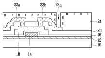
도 1을 참조하면, 기판(10) 상에 버퍼층(12)이 형성되고, 버퍼층(12) 상에 게이트 전극(14)이 형성된다. 게이트 전극(14)을 포함하는 버퍼층(12) 상에는 제 1 절연층(16)이 형성되고, 게이트 전극(14)을 포함하는 제 1 절연층(16) 상에는 산화물 반도체로 이루어진 활성층(18)이 형성된다. 활성층(18)을 포함하는 제 1 절연층(16) 상에는 제 2 절연층(20)이 형성되고, 제 2 절연층(20) 상에는 활성층(18)과 연결되도록 소스 전극 및 드레인 전극(22a 및 22b)이 형성된다.Referring to FIG. 1, a
소스 전극 및 드레인 전극(22a 및 22b)을 포함하는 제 2 절연층(20) 상에는 유기물로 이루어진 제 3 절연층(24)이 형성되고, 제 3 절연층(24) 상에는 소스 전극 또는 드레인 전극(22a 또는 22b)과 연결되며 활성층(18)과 중첩되지 않도록 애노드 전극(26)이 형성된다.A third insulating
애노드 전극(26)을 포함하는 제 3 절연층(24) 상에는 발광영역의 애노드 전극(26)이 노출되도록 패터닝된 화소 정의막(28)이 형성되고, 노출된 애노드 전극(26) 상에는 유기 발광층(30)이 형성되며, 유기 발광층(30)을 포함하는 화소 정의막(28) 상에는 캐소드 전극(32)이 형성된다.A patterned
그러면 상기와 같이 구성된 유기전계발광 표시 장치의 제조 과정을 통해 본 발명을 보다 상세하게 설명하기로 한다.Next, the present invention will be described in more detail through the manufacturing process of the organic light emitting display device configured as described above.
도 2a 내지 도 2e는 본 발명에 따른 유기전계발광 표시 장치의 제조 방법을 설명하기 위한 단면도이다.2A to 2E are cross-sectional views illustrating a method of manufacturing an organic light emitting display device according to the present invention.
도 2a을 참조하면, 유리나 플라스틱으로 이루어진 절연 기판(10) 상에 버퍼층(12) 및 금속층을 형성하고, 금속층을 패터닝하여 게이트 전극(14)을 형성한다. 게이트 전극(14)을 포함하는 버퍼층(12) 상에 제 1 절연층(16) 및 산화물 반도체층을 형성하고, 산화물 반도체층을 패터닝하여 게이트 전극(14a)을 포함하는 제 1 절연층(16) 상에 활성층(18)을 형성한다.Referring to FIG. 2A, a
금속층은 텅스텐(W), 티타늄(Ti), 몰리브덴(Mo), 은(Ag), 탄탈륨(Ta), 알루미늄(Al), 구리(Cu), 금(Au), 크롬(Cr) 및 니오비움(Nb) 등의 금속이나 상기 금속들의 합금으로 형성하고, 산화물 반도체층은 산화아연(ZnO)으로 형성하거나, 산화아연(ZnO)에 인듐(In), 갈륨(Ga), 하프늄(Hf), 스태늄(Sn) 등이 도핑된 예를 들어, InZnO(IZO), GaInZnO(GIZO), HfInZnO 등으로 형성한다.Metal layers include tungsten (W), titanium (Ti), molybdenum (Mo), silver (Ag), tantalum (Ta), aluminum (Al), copper (Cu), gold (Au), chromium (Cr) and niobium ( Nb) or an alloy of the above metals, and the oxide semiconductor layer is formed of zinc oxide (ZnO), or indium (In), gallium (Ga), hafnium (Hf), or titanium in zinc oxide (ZnO). (Sn) or the like is formed of, for example, InZnO (IZO), GaInZnO (GIZO), HfInZnO, or the like.
도 2b를 참조하면, 활성층(18)을 포함하는 제 1 절연층(16) 상에 제 2 절연층(20)을 형성하고, 활성층(18)의 일부 영역(소스 영역 및 드레인 영역)이 노출되도록 콘택홀을 형성한다. 콘택홀이 매립되도록 제 2 절연층(20) 상에 금속층을 형성한 후 패터닝하여 소스 영역 및 드레인 영역의 활성층(18)과 연결되는 소스 전극 및 드레인 전극(22a 및 22b)을 형성한다. 금속층은 텅스텐(W), 티타늄(Ti), 몰리브덴(Mo), 은(Ag), 탄탈륨(Ta), 알루미늄(Al), 구리(Cu), 금(Au), 크롬(Cr) 및 니오비움(Nb) 등의 금속이나 상기 금속들의 합금으로 형성한다.Referring to FIG. 2B, the second
소스 전극 및 드레인 전극(22a 및 22b)을 형성하기 위해 금속층을 패터닝하는 과정에서 제 2 절연층(20)을 식각 정지층(etch stop layer)로 이용한다. 패터닝 과정은 건식 식각을 포함하지만, 채널 영역의 활성층(18) 상에 제 2 절연층(20)이 형성되어 있으므로 활성층(18)의 피해(damage)로 인한 전기적 특성 변화가 방지될 수 있다.In the process of patterning the metal layer to form the source and
도 2c를 참조하면, 소스 전극 및 드레인 전극(22a 및 22b)을 포함하는 제 2 절연층(20) 상에 절연 및 평탄화를 위하여 제 3 절연층(24)을 형성한다. 제 3 절연층(24)은 아크릴(acrylic) 및 폴리이미드(polyimid)와 같은 유기물로 형성한다. 이 때 공정 조건에 따라 무기물 절연층(도시안됨)을 형성하고, 무기물 절연층 상에 제 3 절연층(24)을 형성할 수도 있다.Referring to FIG. 2C, a third
제 3 절연층(24)을 패터닝하여 소스 전극 또는 드레인 전극(22a 또는 22b)이 노출되도록 비아홀(24a)을 형성하고, 세정 공정을 진행하여 식각 부산물 및 오염 물질을 제거한다. 이 때 세정액에 물(H2O)이 포함될 경우 유기물로 이루어진 제 3 절연층(24)에 수소(H)가 침투될 수 있다.The third
도 2d를 참조하면, 비아홀(24a)이 매립되도록 제 3 절연층(24) 상에 ITO(Indium Tin Oxide) 및 IZO(Indium Zinc Oxide)와 같은 투명한 도전층을 형성한 후 패터닝하여 소스 전극 또는 드레인 전극(22a 또는 22b)과 연결되는 애노드 전극(26)을 형성한다. 이 때 애노드 전극(26)은 활성층(18)과 중첩되지 않도록 형성한다.Referring to FIG. 2D, a transparent conductive layer such as indium tin oxide (ITO) and indium zinc oxide (IZO) is formed on the third insulating
애노드 전극(26)을 포함하는 제 3 절연층(24) 상에 화소 정의막(28)을 형성한 후 패터닝하여 발광 영역의 애노드 전극(26)을 노출시킨다. 화소 정의막(28)은 코팅 및 열처리 공정을 통해 형성될 수 있다.The
열처리 과정에서 제 3 절연층(24)에 침투된 수소(H)는 외부로 확산되는데, 애노드 전극(26)의 하부에서는 외부로 확산되지 못하지만, 애노드 전극(26) 이외의 부분에서는 외부로 쉽게 확산되기 때문에 활성층(18)으로 침투되지 않는다.In the heat treatment process, the hydrogen H penetrated into the third insulating
만일, 산화물 반도체층(18)으로 수소(H)가 침투되면 케리어 농도가 증가하여 전도성을 갖게 되기 때문에 문턱전압(Vth)이 변화되거나 박막 트랜지스터로 사용할 수 없게 된다.If hydrogen (H) penetrates into the
따라서 수소(H)의 외부 확산을 촉진시키기 위해서 후속 제조 과정에 열처리가 포함되는 것이 바람직하다.Therefore, it is preferable to include heat treatment in the subsequent manufacturing process in order to promote the external diffusion of hydrogen (H).
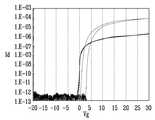
도 3a는 활성층(18) 상부에 애노드 전극(26)이 배치되지 않는 본 발명의 구조를 갖는 박막 트랜지스터의 문턱전압 특성을 측정한 그래프이고, 도 3b는 활성층 상부에 애노드 전극이 배치된 구조를 갖는 박막 트랜지스터의 문턱전압 특성을 측정한 그래프이다.3A is a graph measuring threshold voltage characteristics of a thin film transistor having a structure of the present invention in which an
게이트 전압(Vg)에 따른 드레인 전류(Id)의 변화를 측정한 결과, 본 발명의 구조를 갖는 박막 트랜지스터는 안정된 문턱전압 특성을 나타내는 반면, 활성층 상부에 애노드 전극이 배치된 구조를 갖는 박막 트랜지스터는 문턱전압이 불안정하게 변화되거나 전도성을 나타내었다.As a result of measuring the change of the drain current Id according to the gate voltage Vg, the thin film transistor having the structure of the present invention shows stable threshold voltage characteristics, whereas the thin film transistor having the structure in which the anode is disposed on the active layer Threshold voltage changed unstable or showed conductivity.
도 2e를 참조하면, 발광영역의 노출된 애노드 전극(26) 상에 유기 발광 층(30)을 형성하고, 유기 발광층(30)을 포함하는 화소 정의막(28) 상에 캐소드 전극(32)을 형성한다.Referring to FIG. 2E, the
본 발명의 유기전계발광 표시 장치는 외부로부터 제공되는 신호가 박막 트랜지스터에 의해 애노드 전극(26)으로 제공된다. 따라서 애노드 전극(26) 및 캐소드 전극(32)에 소정의 전압이 인가되면 애노드 전극(26)을 통해 주입되는 정공과 캐소드 전극(32)을 통해 주입되는 전자가 유기 발광층(30)에서 재결합하게 되고, 이 과정에서 발생되는 에너지 차이에 의해 유기 발광층(30)으로부터 방출된 광이 외부로 출사됨으로써 문자나 화상을 표시한다.In the organic light emitting display device of the present invention, a signal provided from the outside is provided to the
본 발명의 유기전계발광 표시 장치는 제조 과정에서 산화물 반도체층의 전기적 특성 변화가 발생되지 않기 때문에 안정된 문턱전압 특성을 유지할 수 있으며, 이에 따라 화질 및 신뢰성이 우수한 표시 장치의 구현이 가능해진다.The organic light emitting display device of the present invention can maintain a stable threshold voltage characteristic because no change in electrical characteristics of the oxide semiconductor layer is produced in the manufacturing process, thereby realizing a display device having excellent image quality and reliability.
이상에서와 같이 상세한 설명과 도면을 통해 본 발명의 최적 실시예를 개시하였다. 용어들은 단지 본 발명을 설명하기 위한 목적에서 사용된 것이지 의미 한정이나 특허청구범위에 기재된 본 발명의 범위를 제한하기 위하여 사용된 것은 아니다. 그러므로 본 기술 분야의 통상의 지식을 가진 자라면 이로부터 다양한 변형 및 균등한 타 실시예가 가능하다는 점을 이해할 것이다. 따라서 본 발명의 진정한 기술적 보호 범위는 첨부된 특허청구범위의 기술적 사상에 의해 정해져야 할 것이다.As described above, the preferred embodiment of the present invention has been disclosed through the detailed description and the drawings. The terms are used only for the purpose of describing the present invention and are not used to limit the scope of the present invention as defined in the meaning or claims. Therefore, those skilled in the art will understand that various modifications and equivalent other embodiments are possible from this. Therefore, the true technical protection scope of the present invention will be defined by the technical spirit of the appended claims.
도 1은 본 발명에 따른 유기전계발광 표시 장치를 설명하기 위한 단면도.1 is a cross-sectional view illustrating an organic light emitting display device according to an exemplary embodiment of the present invention.
도 2a 내지 도 2e는 본 발명에 따른 유기전계발광 표시 장치의 제조 방법을 설명하기 위한 단면도.2A to 2E are cross-sectional views illustrating a method of manufacturing an organic light emitting display device according to the present invention.
도 3a 및 도 3b는 게이트 전압(Vg)에 따른 드레인 전류(Id)의 변화를 측정한 그래프.3A and 3B are graphs illustrating changes in the drain current Id according to the gate voltage Vg.
<도면의 주요 부분에 대한 부호의 설명><Explanation of symbols for the main parts of the drawings>
10: 기판12: 버퍼층10
14: 게이트 전극16: 제 1 절연층14: gate electrode 16: first insulating layer
18: 활성층20: 제 2 절연층18: active layer 20: second insulating layer
22a: 소스 전극22b: 드레인 전극22a:
24: 제 3 절연층26: 애노드 전극24: third insulating layer 26: anode electrode
28: 화소 정의막30: 유기 발광층28: pixel defining layer 30: organic light emitting layer
32: 캐소드 전극32: cathode electrode
Claims (10)
Translated fromKoreanPriority Applications (5)
| Application Number | Priority Date | Filing Date | Title |
|---|---|---|---|
| KR1020090105986AKR101082254B1 (en) | 2009-11-04 | 2009-11-04 | Organic light emitting display device and method of manufacturing the same |
| JP2010031410AJP2011100092A (en) | 2009-11-04 | 2010-02-16 | Organic electric field light emitting display device and method of manufacturing the same |
| US12/833,785US8158979B2 (en) | 2009-11-04 | 2010-07-09 | Organic light emitting display and method of manufacturing the same |
| TW099125293ATWI505458B (en) | 2009-11-04 | 2010-07-30 | Method for manufacturing organic light emitting display |
| JP2013066297AJP2013138028A (en) | 2009-11-04 | 2013-03-27 | Organic electroluminescent display device manufacturing method |
Applications Claiming Priority (1)
| Application Number | Priority Date | Filing Date | Title |
|---|---|---|---|
| KR1020090105986AKR101082254B1 (en) | 2009-11-04 | 2009-11-04 | Organic light emitting display device and method of manufacturing the same |
Publications (2)
| Publication Number | Publication Date |
|---|---|
| KR20110049126A KR20110049126A (en) | 2011-05-12 |
| KR101082254B1true KR101082254B1 (en) | 2011-11-09 |
Family
ID=43924427
Family Applications (1)
| Application Number | Title | Priority Date | Filing Date |
|---|---|---|---|
| KR1020090105986AActiveKR101082254B1 (en) | 2009-11-04 | 2009-11-04 | Organic light emitting display device and method of manufacturing the same |
Country Status (4)
| Country | Link |
|---|---|
| US (1) | US8158979B2 (en) |
| JP (2) | JP2011100092A (en) |
| KR (1) | KR101082254B1 (en) |
| TW (1) | TWI505458B (en) |
Families Citing this family (9)
| Publication number | Priority date | Publication date | Assignee | Title |
|---|---|---|---|---|
| KR101073272B1 (en)* | 2009-11-04 | 2011-10-12 | 삼성모바일디스플레이주식회사 | Method of manufacturing organic light emitting display device |
| US9219159B2 (en) | 2011-03-25 | 2015-12-22 | Semiconductor Energy Laboratory Co., Ltd. | Method for forming oxide semiconductor film and method for manufacturing semiconductor device |
| TWI545652B (en) | 2011-03-25 | 2016-08-11 | 半導體能源研究所股份有限公司 | Semiconductor device and method of manufacturing same |
| US9012904B2 (en)* | 2011-03-25 | 2015-04-21 | Semiconductor Energy Laboratory Co., Ltd. | Semiconductor device and method for manufacturing the same |
| KR20210078571A (en) | 2012-03-13 | 2021-06-28 | 가부시키가이샤 한도오따이 에네루기 켄큐쇼 | Light-emitting device and method for driving the same |
| US9806098B2 (en) | 2013-12-10 | 2017-10-31 | Semiconductor Energy Laboratory Co., Ltd. | Light-emitting device |
| CN104810382A (en)* | 2015-05-07 | 2015-07-29 | 深圳市华星光电技术有限公司 | AMOLED (active matrix/organic light emitting diode) backboard production method and AMOLED backboard structure |
| US9768254B2 (en)* | 2015-07-30 | 2017-09-19 | International Business Machines Corporation | Leakage-free implantation-free ETSOI transistors |
| KR102491882B1 (en)* | 2017-12-20 | 2023-01-27 | 삼성디스플레이 주식회사 | Organic light emitting display and method of manufacturing thereof |
Family Cites Families (33)
| Publication number | Priority date | Publication date | Assignee | Title |
|---|---|---|---|---|
| US6580475B2 (en)* | 2000-04-27 | 2003-06-17 | Semiconductor Energy Laboratory Co., Ltd. | Semiconductor device and method of fabricating the same |
| US6825496B2 (en)* | 2001-01-17 | 2004-11-30 | Semiconductor Energy Laboratory Co., Ltd. | Light emitting device |
| JP4310984B2 (en)* | 2002-02-06 | 2009-08-12 | 株式会社日立製作所 | Organic light emitting display |
| JP2005149942A (en)* | 2003-11-17 | 2005-06-09 | Seiko Epson Corp | Electro-optical device, manufacturing method thereof, and electronic apparatus |
| US7247529B2 (en)* | 2004-08-30 | 2007-07-24 | Semiconductor Energy Laboratory Co., Ltd. | Method for manufacturing display device |
| US20060197092A1 (en) | 2005-03-03 | 2006-09-07 | Randy Hoffman | System and method for forming conductive material on a substrate |
| JP5116225B2 (en) | 2005-09-06 | 2013-01-09 | キヤノン株式会社 | Manufacturing method of oxide semiconductor device |
| JP5089139B2 (en)* | 2005-11-15 | 2012-12-05 | 株式会社半導体エネルギー研究所 | Method for manufacturing semiconductor device |
| US8017950B2 (en)* | 2005-12-29 | 2011-09-13 | Lg Display Co., Ltd. | Organic electro-luminescence display device and method of manfacturing the same |
| KR100768199B1 (en)* | 2006-01-02 | 2007-10-17 | 삼성에스디아이 주식회사 | Organic thin film transistor and organic light emitting display device having same |
| JP4655942B2 (en)* | 2006-01-16 | 2011-03-23 | セイコーエプソン株式会社 | LIGHT EMITTING DEVICE, LIGHT EMITTING DEVICE MANUFACTURING METHOD, AND ELECTRONIC DEVICE |
| KR20080016282A (en)* | 2006-08-18 | 2008-02-21 | 삼성전자주식회사 | Display device and manufacturing method |
| US20080048191A1 (en)* | 2006-08-23 | 2008-02-28 | Hyun Chul Son | Organic light emitting display device and method of fabricating the same |
| TWI442368B (en)* | 2006-10-26 | 2014-06-21 | Semiconductor Energy Lab | Electronic device, display device, and semiconductor device, and driving method thereof |
| JP2008134625A (en)* | 2006-10-26 | 2008-06-12 | Semiconductor Energy Lab Co Ltd | Semiconductor device, display device and electronic apparatus |
| JP2008166168A (en)* | 2006-12-28 | 2008-07-17 | Canon Inc | Organic EL display and its manufacturing method |
| JP5197058B2 (en)* | 2007-04-09 | 2013-05-15 | キヤノン株式会社 | Light emitting device and manufacturing method thereof |
| JP2009031742A (en)* | 2007-04-10 | 2009-02-12 | Fujifilm Corp | Organic electroluminescence display |
| KR100882909B1 (en)* | 2007-06-27 | 2009-02-10 | 삼성모바일디스플레이주식회사 | Thin film transistor, manufacturing method thereof, organic light emitting display device comprising same, and manufacturing method thereof |
| KR100875101B1 (en)* | 2007-08-08 | 2008-12-19 | 삼성모바일디스플레이주식회사 | Organic light emitting display and manufacturing method of organic light emitting display |
| KR100889626B1 (en)* | 2007-08-22 | 2009-03-20 | 삼성모바일디스플레이주식회사 | Thin film transistor, manufacturing method thereof, organic light emitting display device having same, and manufacturing method thereof |
| JP5354999B2 (en) | 2007-09-26 | 2013-11-27 | キヤノン株式会社 | Method for manufacturing field effect transistor |
| JP5213422B2 (en)* | 2007-12-04 | 2013-06-19 | キヤノン株式会社 | Oxide semiconductor element having insulating layer and display device using the same |
| KR100965260B1 (en)* | 2008-01-25 | 2010-06-22 | 삼성모바일디스플레이주식회사 | Thin film transistor, manufacturing method thereof and organic light emitting display device having same |
| JP2009224063A (en)* | 2008-03-13 | 2009-10-01 | Fuji Electric Holdings Co Ltd | Method of manufacturing color conversion filter substrate |
| KR100936871B1 (en) | 2008-04-03 | 2010-01-14 | 삼성모바일디스플레이주식회사 | Organic light emitting display device and manufacturing method thereof |
| KR100982311B1 (en)* | 2008-05-26 | 2010-09-15 | 삼성모바일디스플레이주식회사 | Thin film transistor, manufacturing method thereof and organic light emitting display device comprising same |
| KR100963026B1 (en)* | 2008-06-30 | 2010-06-10 | 삼성모바일디스플레이주식회사 | Thin film transistor, its manufacturing method, and flat panel display device comprising thin film transistor |
| KR101910451B1 (en)* | 2008-07-10 | 2018-10-22 | 가부시키가이샤 한도오따이 에네루기 켄큐쇼 | Light-emitting device and electronic device using the same |
| KR101352237B1 (en)* | 2008-08-13 | 2014-01-16 | 엘지디스플레이 주식회사 | Organic Light Emitting Display and Manufacturing Method of the same |
| KR101545315B1 (en)* | 2008-09-17 | 2015-08-20 | 삼성디스플레이 주식회사 | Organic electroluminescent device |
| KR101073272B1 (en)* | 2009-11-04 | 2011-10-12 | 삼성모바일디스플레이주식회사 | Method of manufacturing organic light emitting display device |
| KR101082174B1 (en)* | 2009-11-27 | 2011-11-09 | 삼성모바일디스플레이주식회사 | Organic light emitting display device and method of manufacturing the same |
- 2009
- 2009-11-04KRKR1020090105986Apatent/KR101082254B1/enactiveActive
- 2010
- 2010-02-16JPJP2010031410Apatent/JP2011100092A/enactivePending
- 2010-07-09USUS12/833,785patent/US8158979B2/enactiveActive
- 2010-07-30TWTW099125293Apatent/TWI505458B/enactive
- 2013
- 2013-03-27JPJP2013066297Apatent/JP2013138028A/enactivePending
Also Published As
| Publication number | Publication date |
|---|---|
| JP2011100092A (en) | 2011-05-19 |
| TWI505458B (en) | 2015-10-21 |
| US8158979B2 (en) | 2012-04-17 |
| JP2013138028A (en) | 2013-07-11 |
| US20110101330A1 (en) | 2011-05-05 |
| KR20110049126A (en) | 2011-05-12 |
| TW201117372A (en) | 2011-05-16 |
Similar Documents
| Publication | Publication Date | Title |
|---|---|---|
| KR101073272B1 (en) | Method of manufacturing organic light emitting display device | |
| KR101082254B1 (en) | Organic light emitting display device and method of manufacturing the same | |
| KR100907400B1 (en) | Thin film transistor and light emitting display device using same | |
| TWI524514B (en) | Method for manufacturing organic light emitting display device | |
| KR100958006B1 (en) | Thin film transistor, its manufacturing method, and flat panel display device comprising thin film transistor | |
| JP5584960B2 (en) | Thin film transistor and display device | |
| US20230099934A1 (en) | Thin film transistor, array substrate, and method for fabricating array substrate | |
| KR100936871B1 (en) | Organic light emitting display device and manufacturing method thereof | |
| US9748276B2 (en) | Thin film transistor and method of manufacturing the same, array substrate and display device | |
| KR20090124527A (en) | Thin film transistor, its manufacturing method, and flat panel display device comprising thin film transistor | |
| KR20110037220A (en) | An organic light emitting display device comprising a thin film transistor, a method of manufacturing the same, and a thin film transistor | |
| CN103730510B (en) | A kind of thin film transistor (TFT) and preparation method thereof, array base palte, display device | |
| JP2016111107A (en) | Thin film transistor, manufacturing method of the same and display device | |
| KR101064470B1 (en) | Thin film transistor and its manufacturing method | |
| JP2022146789A (en) | thin film transistor substrate | |
| KR20090105561A (en) | Semiconductor device and flat panel display device having same | |
| KR100991559B1 (en) | Method for manufacturing thin film transistor and thin film transistor manufactured thereby | |
| KR102172972B1 (en) | Thin film transistor and method for fabricating the same | |
| KR101022141B1 (en) | An organic light emitting display device comprising a thin film transistor, a method of manufacturing the same, and a thin film transistor | |
| JP2016111105A (en) | Thin film transistor, manufacturing method thereof, and display device | |
| KR20210004356A (en) | Display device having an oxide semiconductor pattern | |
| KR100982314B1 (en) | Thin film transistor, manufacturing method thereof and organic light emitting display device comprising same | |
| KR20150075733A (en) | Thin film transistor and flat panel display device having the same | |
| KR100796592B1 (en) | Thin film transistor and its manufacturing method | |
| KR20130040342A (en) | Thin film transistor and method of fabricating the same |
Legal Events
| Date | Code | Title | Description |
|---|---|---|---|
| A201 | Request for examination | ||
| PA0109 | Patent application | Patent event code:PA01091R01D Comment text:Patent Application Patent event date:20091104 | |
| PA0201 | Request for examination | ||
| E902 | Notification of reason for refusal | ||
| PE0902 | Notice of grounds for rejection | Comment text:Notification of reason for refusal Patent event date:20110314 Patent event code:PE09021S01D | |
| PG1501 | Laying open of application | ||
| E701 | Decision to grant or registration of patent right | ||
| PE0701 | Decision of registration | Patent event code:PE07011S01D Comment text:Decision to Grant Registration Patent event date:20111020 | |
| GRNT | Written decision to grant | ||
| PR0701 | Registration of establishment | Comment text:Registration of Establishment Patent event date:20111103 Patent event code:PR07011E01D | |
| PR1002 | Payment of registration fee | Payment date:20111103 End annual number:3 Start annual number:1 | |
| PG1601 | Publication of registration | ||
| FPAY | Annual fee payment | Payment date:20141030 Year of fee payment:4 | |
| PR1001 | Payment of annual fee | Payment date:20141030 Start annual number:4 End annual number:4 | |
| FPAY | Annual fee payment | Payment date:20151030 Year of fee payment:5 | |
| PR1001 | Payment of annual fee | Payment date:20151030 Start annual number:5 End annual number:5 | |
| FPAY | Annual fee payment | Payment date:20171101 Year of fee payment:7 | |
| PR1001 | Payment of annual fee | Payment date:20171101 Start annual number:7 End annual number:7 | |
| FPAY | Annual fee payment | Payment date:20181101 Year of fee payment:8 | |
| PR1001 | Payment of annual fee | Payment date:20181101 Start annual number:8 End annual number:8 | |
| FPAY | Annual fee payment | Payment date:20191028 Year of fee payment:9 | |
| PR1001 | Payment of annual fee | Payment date:20191028 Start annual number:9 End annual number:9 | |
| PR1001 | Payment of annual fee | Payment date:20201102 Start annual number:10 End annual number:10 | |
| PR1001 | Payment of annual fee | Payment date:20211027 Start annual number:11 End annual number:11 | |
| PR1001 | Payment of annual fee | Payment date:20221025 Start annual number:12 End annual number:12 | |
| PR1001 | Payment of annual fee | Payment date:20231023 Start annual number:13 End annual number:13 | |
| PR1001 | Payment of annual fee | Payment date:20241022 Start annual number:14 End annual number:14 |