KR101081135B1 - Light emitting device, method for fabricating the light emitting device and light emitting device package - Google Patents
Light emitting device, method for fabricating the light emitting device and light emitting device packageDownload PDFInfo
- Publication number
- KR101081135B1 KR101081135B1KR1020100022754AKR20100022754AKR101081135B1KR 101081135 B1KR101081135 B1KR 101081135B1KR 1020100022754 AKR1020100022754 AKR 1020100022754AKR 20100022754 AKR20100022754 AKR 20100022754AKR 101081135 B1KR101081135 B1KR 101081135B1
- Authority
- KR
- South Korea
- Prior art keywords
- light emitting
- layer
- emitting device
- electrode
- semiconductor layer
- Prior art date
- Legal status (The legal status is an assumption and is not a legal conclusion. Google has not performed a legal analysis and makes no representation as to the accuracy of the status listed.)
- Expired - Fee Related
Links
Images


Classifications
- H—ELECTRICITY
- H10—SEMICONDUCTOR DEVICES; ELECTRIC SOLID-STATE DEVICES NOT OTHERWISE PROVIDED FOR
- H10H—INORGANIC LIGHT-EMITTING SEMICONDUCTOR DEVICES HAVING POTENTIAL BARRIERS
- H10H20/00—Individual inorganic light-emitting semiconductor devices having potential barriers, e.g. light-emitting diodes [LED]
- H10H20/80—Constructional details
- H10H20/84—Coatings, e.g. passivation layers or antireflective coatings
- H—ELECTRICITY
- H10—SEMICONDUCTOR DEVICES; ELECTRIC SOLID-STATE DEVICES NOT OTHERWISE PROVIDED FOR
- H10H—INORGANIC LIGHT-EMITTING SEMICONDUCTOR DEVICES HAVING POTENTIAL BARRIERS
- H10H20/00—Individual inorganic light-emitting semiconductor devices having potential barriers, e.g. light-emitting diodes [LED]
- H10H20/80—Constructional details
- H10H20/81—Bodies
- H10H20/811—Bodies having quantum effect structures or superlattices, e.g. tunnel junctions
- H10H20/812—Bodies having quantum effect structures or superlattices, e.g. tunnel junctions within the light-emitting regions, e.g. having quantum confinement structures
- H—ELECTRICITY
- H10—SEMICONDUCTOR DEVICES; ELECTRIC SOLID-STATE DEVICES NOT OTHERWISE PROVIDED FOR
- H10H—INORGANIC LIGHT-EMITTING SEMICONDUCTOR DEVICES HAVING POTENTIAL BARRIERS
- H10H20/00—Individual inorganic light-emitting semiconductor devices having potential barriers, e.g. light-emitting diodes [LED]
- H10H20/80—Constructional details
- H10H20/81—Bodies
- H10H20/822—Materials of the light-emitting regions
- H10H20/824—Materials of the light-emitting regions comprising only Group III-V materials, e.g. GaP
- H10H20/825—Materials of the light-emitting regions comprising only Group III-V materials, e.g. GaP containing nitrogen, e.g. GaN
- H—ELECTRICITY
- H10—SEMICONDUCTOR DEVICES; ELECTRIC SOLID-STATE DEVICES NOT OTHERWISE PROVIDED FOR
- H10H—INORGANIC LIGHT-EMITTING SEMICONDUCTOR DEVICES HAVING POTENTIAL BARRIERS
- H10H20/00—Individual inorganic light-emitting semiconductor devices having potential barriers, e.g. light-emitting diodes [LED]
- H10H20/80—Constructional details
- H10H20/83—Electrodes
- H10H20/831—Electrodes characterised by their shape
- H10H20/8316—Multi-layer electrodes comprising at least one discontinuous layer
- H—ELECTRICITY
- H10—SEMICONDUCTOR DEVICES; ELECTRIC SOLID-STATE DEVICES NOT OTHERWISE PROVIDED FOR
- H10H—INORGANIC LIGHT-EMITTING SEMICONDUCTOR DEVICES HAVING POTENTIAL BARRIERS
- H10H20/00—Individual inorganic light-emitting semiconductor devices having potential barriers, e.g. light-emitting diodes [LED]
- H10H20/80—Constructional details
- H10H20/83—Electrodes
- H10H20/832—Electrodes characterised by their material
- H10H20/833—Transparent materials
- H—ELECTRICITY
- H10—SEMICONDUCTOR DEVICES; ELECTRIC SOLID-STATE DEVICES NOT OTHERWISE PROVIDED FOR
- H10H—INORGANIC LIGHT-EMITTING SEMICONDUCTOR DEVICES HAVING POTENTIAL BARRIERS
- H10H20/00—Individual inorganic light-emitting semiconductor devices having potential barriers, e.g. light-emitting diodes [LED]
- H10H20/80—Constructional details
- H10H20/85—Packages
- H10H20/852—Encapsulations
- H10H20/854—Encapsulations characterised by their material, e.g. epoxy or silicone resins
- F—MECHANICAL ENGINEERING; LIGHTING; HEATING; WEAPONS; BLASTING
- F21—LIGHTING
- F21K—NON-ELECTRIC LIGHT SOURCES USING LUMINESCENCE; LIGHT SOURCES USING ELECTROCHEMILUMINESCENCE; LIGHT SOURCES USING CHARGES OF COMBUSTIBLE MATERIAL; LIGHT SOURCES USING SEMICONDUCTOR DEVICES AS LIGHT-GENERATING ELEMENTS; LIGHT SOURCES NOT OTHERWISE PROVIDED FOR
- F21K9/00—Light sources using semiconductor devices as light-generating elements, e.g. using light-emitting diodes [LED] or lasers
- F21K9/20—Light sources comprising attachment means
- F21K9/23—Retrofit light sources for lighting devices with a single fitting for each light source, e.g. for substitution of incandescent lamps with bayonet or threaded fittings
- F—MECHANICAL ENGINEERING; LIGHTING; HEATING; WEAPONS; BLASTING
- F21—LIGHTING
- F21Y—INDEXING SCHEME ASSOCIATED WITH SUBCLASSES F21K, F21L, F21S and F21V, RELATING TO THE FORM OR THE KIND OF THE LIGHT SOURCES OR OF THE COLOUR OF THE LIGHT EMITTED
- F21Y2105/00—Planar light sources
- F21Y2105/10—Planar light sources comprising a two-dimensional array of point-like light-generating elements
- F—MECHANICAL ENGINEERING; LIGHTING; HEATING; WEAPONS; BLASTING
- F21—LIGHTING
- F21Y—INDEXING SCHEME ASSOCIATED WITH SUBCLASSES F21K, F21L, F21S and F21V, RELATING TO THE FORM OR THE KIND OF THE LIGHT SOURCES OR OF THE COLOUR OF THE LIGHT EMITTED
- F21Y2113/00—Combination of light sources
- F21Y2113/10—Combination of light sources of different colours
- F21Y2113/13—Combination of light sources of different colours comprising an assembly of point-like light sources
- F—MECHANICAL ENGINEERING; LIGHTING; HEATING; WEAPONS; BLASTING
- F21—LIGHTING
- F21Y—INDEXING SCHEME ASSOCIATED WITH SUBCLASSES F21K, F21L, F21S and F21V, RELATING TO THE FORM OR THE KIND OF THE LIGHT SOURCES OR OF THE COLOUR OF THE LIGHT EMITTED
- F21Y2115/00—Light-generating elements of semiconductor light sources
- F21Y2115/10—Light-emitting diodes [LED]
- H—ELECTRICITY
- H01—ELECTRIC ELEMENTS
- H01L—SEMICONDUCTOR DEVICES NOT COVERED BY CLASS H10
- H01L2224/00—Indexing scheme for arrangements for connecting or disconnecting semiconductor or solid-state bodies and methods related thereto as covered by H01L24/00
- H01L2224/01—Means for bonding being attached to, or being formed on, the surface to be connected, e.g. chip-to-package, die-attach, "first-level" interconnects; Manufacturing methods related thereto
- H01L2224/42—Wire connectors; Manufacturing methods related thereto
- H01L2224/47—Structure, shape, material or disposition of the wire connectors after the connecting process
- H01L2224/48—Structure, shape, material or disposition of the wire connectors after the connecting process of an individual wire connector
- H01L2224/4805—Shape
- H01L2224/4809—Loop shape
- H01L2224/48091—Arched
- H—ELECTRICITY
- H01—ELECTRIC ELEMENTS
- H01L—SEMICONDUCTOR DEVICES NOT COVERED BY CLASS H10
- H01L2224/00—Indexing scheme for arrangements for connecting or disconnecting semiconductor or solid-state bodies and methods related thereto as covered by H01L24/00
- H01L2224/01—Means for bonding being attached to, or being formed on, the surface to be connected, e.g. chip-to-package, die-attach, "first-level" interconnects; Manufacturing methods related thereto
- H01L2224/42—Wire connectors; Manufacturing methods related thereto
- H01L2224/47—Structure, shape, material or disposition of the wire connectors after the connecting process
- H01L2224/48—Structure, shape, material or disposition of the wire connectors after the connecting process of an individual wire connector
- H01L2224/481—Disposition
- H01L2224/48151—Connecting between a semiconductor or solid-state body and an item not being a semiconductor or solid-state body, e.g. chip-to-substrate, chip-to-passive
- H01L2224/48221—Connecting between a semiconductor or solid-state body and an item not being a semiconductor or solid-state body, e.g. chip-to-substrate, chip-to-passive the body and the item being stacked
- H01L2224/48245—Connecting between a semiconductor or solid-state body and an item not being a semiconductor or solid-state body, e.g. chip-to-substrate, chip-to-passive the body and the item being stacked the item being metallic
- H01L2224/48247—Connecting between a semiconductor or solid-state body and an item not being a semiconductor or solid-state body, e.g. chip-to-substrate, chip-to-passive the body and the item being stacked the item being metallic connecting the wire to a bond pad of the item
- H—ELECTRICITY
- H01—ELECTRIC ELEMENTS
- H01L—SEMICONDUCTOR DEVICES NOT COVERED BY CLASS H10
- H01L2224/00—Indexing scheme for arrangements for connecting or disconnecting semiconductor or solid-state bodies and methods related thereto as covered by H01L24/00
- H01L2224/01—Means for bonding being attached to, or being formed on, the surface to be connected, e.g. chip-to-package, die-attach, "first-level" interconnects; Manufacturing methods related thereto
- H01L2224/42—Wire connectors; Manufacturing methods related thereto
- H01L2224/47—Structure, shape, material or disposition of the wire connectors after the connecting process
- H01L2224/48—Structure, shape, material or disposition of the wire connectors after the connecting process of an individual wire connector
- H01L2224/481—Disposition
- H01L2224/48151—Connecting between a semiconductor or solid-state body and an item not being a semiconductor or solid-state body, e.g. chip-to-substrate, chip-to-passive
- H01L2224/48221—Connecting between a semiconductor or solid-state body and an item not being a semiconductor or solid-state body, e.g. chip-to-substrate, chip-to-passive the body and the item being stacked
- H01L2224/48245—Connecting between a semiconductor or solid-state body and an item not being a semiconductor or solid-state body, e.g. chip-to-substrate, chip-to-passive the body and the item being stacked the item being metallic
- H01L2224/48257—Connecting between a semiconductor or solid-state body and an item not being a semiconductor or solid-state body, e.g. chip-to-substrate, chip-to-passive the body and the item being stacked the item being metallic connecting the wire to a die pad of the item
- H—ELECTRICITY
- H01—ELECTRIC ELEMENTS
- H01L—SEMICONDUCTOR DEVICES NOT COVERED BY CLASS H10
- H01L2924/00—Indexing scheme for arrangements or methods for connecting or disconnecting semiconductor or solid-state bodies as covered by H01L24/00
- H01L2924/0001—Technical content checked by a classifier
- H01L2924/0002—Not covered by any one of groups H01L24/00, H01L24/00 and H01L2224/00
- H—ELECTRICITY
- H01—ELECTRIC ELEMENTS
- H01L—SEMICONDUCTOR DEVICES NOT COVERED BY CLASS H10
- H01L2924/00—Indexing scheme for arrangements or methods for connecting or disconnecting semiconductor or solid-state bodies as covered by H01L24/00
- H01L2924/10—Details of semiconductor or other solid state devices to be connected
- H01L2924/11—Device type
- H01L2924/12—Passive devices, e.g. 2 terminal devices
- H01L2924/1203—Rectifying Diode
- H01L2924/12032—Schottky diode
- H—ELECTRICITY
- H10—SEMICONDUCTOR DEVICES; ELECTRIC SOLID-STATE DEVICES NOT OTHERWISE PROVIDED FOR
- H10H—INORGANIC LIGHT-EMITTING SEMICONDUCTOR DEVICES HAVING POTENTIAL BARRIERS
- H10H20/00—Individual inorganic light-emitting semiconductor devices having potential barriers, e.g. light-emitting diodes [LED]
- H10H20/01—Manufacture or treatment
- H10H20/011—Manufacture or treatment of bodies, e.g. forming semiconductor layers
- H10H20/018—Bonding of wafers
- H—ELECTRICITY
- H10—SEMICONDUCTOR DEVICES; ELECTRIC SOLID-STATE DEVICES NOT OTHERWISE PROVIDED FOR
- H10H—INORGANIC LIGHT-EMITTING SEMICONDUCTOR DEVICES HAVING POTENTIAL BARRIERS
- H10H20/00—Individual inorganic light-emitting semiconductor devices having potential barriers, e.g. light-emitting diodes [LED]
- H10H20/80—Constructional details
- H10H20/81—Bodies
- H10H20/814—Bodies having reflecting means, e.g. semiconductor Bragg reflectors
- H—ELECTRICITY
- H10—SEMICONDUCTOR DEVICES; ELECTRIC SOLID-STATE DEVICES NOT OTHERWISE PROVIDED FOR
- H10H—INORGANIC LIGHT-EMITTING SEMICONDUCTOR DEVICES HAVING POTENTIAL BARRIERS
- H10H20/00—Individual inorganic light-emitting semiconductor devices having potential barriers, e.g. light-emitting diodes [LED]
- H10H20/80—Constructional details
- H10H20/81—Bodies
- H10H20/819—Bodies characterised by their shape, e.g. curved or truncated substrates
- H10H20/82—Roughened surfaces, e.g. at the interface between epitaxial layers
Landscapes
- Led Devices (AREA)
Abstract
Translated fromKoreanDescription
Translated fromKorean실시예는 발광 소자, 발광 소자 제조방법 및 발광 소자 패키지에 관한 것이다.The embodiment relates to a light emitting device, a light emitting device manufacturing method and a light emitting device package.
발광 다이오드(LED)는 전기 에너지를 빛으로 변환하는 반도체 소자의 일종이다. 발광 다이오드는 형광등, 백열등 등 기존의 광원에 비해 저소비전력, 반영구적인 수명, 빠른 응답속도, 안전성, 환경친화성의 장점을 가진다. 이에 기존의 광원을 발광 다이오드로 대체하기 위한 많은 연구가 진행되고 있으며, 발광 다이오드는 실내외에서 사용되는 각종 램프, 액정표시장치, 전광판, 가로등 등의 조명 장치의 광원으로서 사용이 증가되고 있는 추세이다.Light emitting diodes (LEDs) are a type of semiconductor device that converts electrical energy into light. Light emitting diodes have the advantages of low power consumption, semi-permanent life, fast response speed, safety and environmental friendliness compared to conventional light sources such as fluorescent and incandescent lamps. Accordingly, many researches are being conducted to replace existing light sources with light emitting diodes, and the use of light emitting diodes is increasing as a light source for lighting devices such as various lamps, liquid crystal displays, electronic displays, and street lamps that are used indoors and outdoors.
실시예는 새로운 구조를 갖는 발광 소자, 발광 소자 제조방법 및 발광 소자 패키지를 제공한다.The embodiment provides a light emitting device, a light emitting device manufacturing method and a light emitting device package having a new structure.
실시예는 신뢰성이 향상된 발광 소자를 제공한다.The embodiment provides a light emitting device having improved reliability.
실시예에 따른 발광 소자는 제1 도전형 반도체층, 상기 제1도전형 반도체층 위에 활성층, 상기 활성층 활성층 위에 제2 도전형 반도체층을 포함하는 발광구조물; 상기 제1 도전형 반도체층의 상면에 접촉된 접합층; 상기 제1 도전형 반도체층 및 상기 접합층의 상면에 접촉된 제1 전극; 및 상기 제2 도전형 반도체층에 전기적으로 연결된 제2 전극을 포함한다.The light emitting device according to the embodiment includes a light emitting structure including a first conductive semiconductor layer, an active layer on the first conductive semiconductor layer, and a second conductive semiconductor layer on the active layer active layer; A bonding layer in contact with an upper surface of the first conductivity type semiconductor layer; A first electrode in contact with an upper surface of the first conductive semiconductor layer and the bonding layer; And a second electrode electrically connected to the second conductivity type semiconductor layer.
실시 예에 따른 발광 소자는, 전도성 지지부재; 상기 전도성 지지부재 위에 제1 도전형 반도체층, 활성층 및 제2 도전형 반도체층을 포함하는 발광구조물; 상기 발광구조물의 상면의 상면에 접촉된 접합층; 및 상기 발광구조물 및 상기 접합층의 상면에 접촉된 제3 전극을 포함한다.The light emitting device according to the embodiment, the conductive support member; A light emitting structure including a first conductive semiconductor layer, an active layer, and a second conductive semiconductor layer on the conductive support member; A bonding layer in contact with an upper surface of the upper surface of the light emitting structure; And a third electrode in contact with an upper surface of the light emitting structure and the bonding layer.
실시 예에 따른 발광소자 패키지는, 몸체; 상기 몸체 위에 적어도 하나의 전극층; 상기 전극층에 전기적으로 연결된 상기의 발광 소자; 및 상기 발광 소자 위에 몰딩 부재를 포함한다.The light emitting device package according to the embodiment includes a body; At least one electrode layer on the body; The light emitting device electrically connected to the electrode layer; And a molding member on the light emitting device.
실시예는 새로운 구조를 갖는 발광 소자, 발광 소자 제조방법 및 발광 소자 패키지를 제공할 수 있다.The embodiment can provide a light emitting device having a new structure, a light emitting device manufacturing method, and a light emitting device package.
실시예는 전극과 화합물 반도체층 사이의 접합력을 개선하여 신뢰성이 향상된 발광 소자를 제공할 수 있다.The embodiment can provide a light emitting device having improved reliability by improving the bonding force between the electrode and the compound semiconductor layer.
도 1은 제1 실시예에 따른 발광 소자의 측단면도
도 2는 도 1의 발광 소자의 상면도
도 3은 도 1의 발광 소자의 A 영역의 확대도
도 4 내지 도 6은 각각 제2 실시예 내지 제4 실시예에 따른 발광 소자의 측단면도를 나타낸 도면
도 7 내지 도 11은 제1 실시예에 따른 발광 소자의 제조방법을 설명하는 도면
도 12는 제5 실시예에 따른 발광 소자의 측단면도
도 13 내지 도 20은 제5 실시예에 따른 발광 소자의 제조방법을 설명하는 도면
도 21은 실시예에 따른 발광 소자를 포함하는 발광 소자 패키지의 단면도1 is a side cross-sectional view of a light emitting device according to the first embodiment
FIG. 2 is a top view of the light emitting device of FIG. 1. FIG.
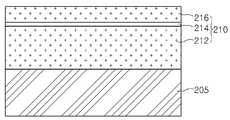
3 is an enlarged view of a region A of the light emitting device of FIG. 1;
4 to 6 are cross-sectional side views of the light emitting devices according to the second to fourth embodiments, respectively.
7 to 11 illustrate a method of manufacturing a light emitting device according to the first embodiment.
12 is a side sectional view of a light emitting device according to the fifth embodiment;
13 to 20 illustrate a method of manufacturing a light emitting device according to the fifth embodiment.
21 is a cross-sectional view of a light emitting device package including a light emitting device according to the embodiment
실시예들의 설명에 있어서, 각 층(막), 영역, 패턴 또는 구조물들이 기판, 각 층(막), 영역, 패드 또는 패턴들의 "위(on)"에 또는 "아래(under)"에 형성되는 것으로 기재되는 경우에 있어, "위(on)"와 "아래(under)"는 "직접(directly)" 또는 "다른 층을 개재하여 (indirectly)" 형성되는 것을 모두 포함한다. 또한 각 층의 위 또는 아래에 대한 기준은 도면을 기준으로 설명한다.In the description of the embodiments, it is to be understood that each layer (film), region, pattern or structure is formed "on" or "under" a substrate, each layer The terms " on "and " under " encompass both being formed" directly "or" indirectly " In addition, the criteria for the top or bottom of each layer will be described with reference to the drawings.
도면에서 각층의 두께나 크기는 설명의 편의 및 명확성을 위하여 과장되거나 생략되거나 또는 개략적으로 도시되었다. 또한 각 구성요소의 크기는 실제크기를 전적으로 반영하는 것은 아니다.In the drawings, the thickness or size of each layer is exaggerated, omitted, or schematically illustrated for convenience and clarity of description. In addition, the size of each component does not necessarily reflect the actual size.
이하, 첨부된 도면을 참조하여 실시예들에 따른 발광 소자, 발광 소자 제조방법 및 발광 소자 패키지에 대해 설명한다.Hereinafter, a light emitting device, a light emitting device manufacturing method, and a light emitting device package according to embodiments will be described with reference to the accompanying drawings.
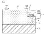
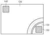
도 1은 제1 실시예에 따른 발광 소자(100)의 측단면도이고, 도 2는 도 1의 발광 소자(100)의 상면도이고, 도 3은 도 1의 발광 소자(100)의 A 영역의 확대도이다.1 is a side cross-sectional view of a
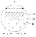
도 1 내지 도 3을 참조하면, 제1 실시예에 따른 발광 소자(100)는 성장기판(105)과, 상기 성장기판(105) 상에 제1 도전형 반도체층(112), 활성층(114) 및 제2 도전형 반도체층(116)이 순차적으로 적층되어 형성되며, 제1 영역(S)은 상기 제1 도전형 반도체층(112)의 상면이 노출되는 발광구조물(110)과, 상기 제1 영역(S)의 상기 제1 도전형 반도체층(112)의 상면이 적어도 일부 노출되도록 형성된 접합층(130)과, 상기 제1 영역(S)의 제1 도전형 반도체층(112) 및 상기 접합층(130) 상에 형성된 제1 전극(150)과, 상기 제2 도전형 반도체층(116) 상에 형성된 투광성전극층(120)과, 상기 제2 도전형 반도체층(116) 및 상기 투광성전극층(120) 상에 형성된 제2 전극(140)을 포함할 수 있다.1 to 3, the
상기 성장기판(105)은 예를 들어, 사파이어(Al2O3) 단결정, SiC, GaAs, GaN, ZnO, Si, GaP, InP, Ge 중 적어도 하나로 형성될 수 있으며, 이에 대해 한정하지는 않는다.The
상기 성장기판(105) 상면에는 상기 발광구조물(110)의 성장을 촉진시키고 발광 소자의 발광 효율을 향상시키기 위해, 소정의 패턴이 형성되거나 경사가 형성될 수 있으며, 이에 대해 한정하지는 않는다.In order to promote growth of the
상기 성장기판(105) 상에는 상기 발광구조물(110)이 성장되어 형성될 수 있다.The
상기 발광구조물(110)은 예를 들어, 상기 제1 도전형 반도체층(112), 활성층(114) 및 제2 도전형 반도체층(116)을 포함할 수 있다. 다만, 상기 성장기판(105)과 상기 발광구조물(110) 사이에는 두 층 사이의 격자 상수 차이를 완화시키고, 상기 발광구조물(110)의 결정성을 향상시키기 위한 버퍼층 또는 언도프트 반도체층이 포함될 수도 있다.The
상기 제1 도전형 반도체층(112)은 예를 들어, n형 반도체층을 포함할 수 있는데, 상기 n형 반도체층은 InxAlyGa1-x-yN (0≤x≤1, 0 ≤y≤1, 0≤x+y≤1)의 조성식을 갖는 반도체 재료, 예를 들어 InAlGaN, GaN, AlGaN, AlInN, InGaN, AlN, InN 등에서 선택될 수 있으며, Si, Ge, Sn 등의 n형 도펀트가 도핑될 수 있다.The first conductivity-
상기 활성층(114)은 예를 들어, InxAlyGa1-x-yN (0≤x≤1, 0 ≤y≤1, 0≤x+y≤1)의 조성식을 가지는 반도체 재료를 포함하여 형성할 수 있으며, 단일 양자 우물 구조, 다중 양자 우물 구조(MQW : Multi Quantum Well), 양자점 구조 또는 양자선 구조 중 어느 하나로 형성될 수 있다.The
상기 활성층(114)은 상기 제1 도전형 반도체층(112) 및 제2 도전형 반도체층(116)으로부터 제공되는 전자 및 정공의 재결합(recombination) 과정에서 발생되는 에너지에 의해 빛을 생성할 수 있다.The
상기 제2 도전형 반도체층(116)은 예를 들어, p형 반도체층으로 구현될 수 있는데, 상기 p형 반도체층은 InxAlyGa1-x-yN (0≤x≤1, 0 ≤y≤1, 0≤x+y≤1)의 조성식을 갖는 반도체 재료, 예를 들어 InAlGaN, GaN, AlGaN, AlInN, InGaN, AlN, InN 등에서 선택될 수 있으며, Mg, Zn, Ca, Sr, Ba 등의 p형 도펀트가 도핑될 수 있다.The second conductivity-
상기 버퍼층(미도시) 및 상기 언도프트 반도체층(미도시)은 InxAlyGa1-x-yN (0≤x≤1, 0 ≤y≤1, 0≤x+y≤1)의 조성식을 갖는 반도체 재료, 예를 들어 InAlGaN, GaN, AlGaN, AlInN, InGaN, AlN, InN 등에서 선택될 수 있으며, 도전성 도펀트가 도핑되지 않아 상기 제1,2 도전형 반도체층(112,116)에 비해 현저히 낮은 전기 전도성을 가질 수 있다.The buffer layer (not shown) and the undoped semiconductor layer (not shown) may have a composition formula of Inx Aly Ga1-xy N (0 ≦ x ≦ 1, 0 ≦ y ≦ 1, 0 ≦ x + y ≦ 1). It may be selected from a semiconductor material having, for example, InAlGaN, GaN, AlGaN, AlInN, InGaN, AlN, InN, etc., do not doped with a conductive dopant significantly lower electrical conductivity than the first and second
상기 발광구조물(110)의 제2 도전형 반도체층(116) 상에는 상기 투광성전극층(120)이 형성될 수 있다. 상기 투광성전극층(120)은 전류를 스프레딩 시킴으로써 전류가 상기 제2 전극(140) 주변으로 편중되는 것을 방지할 수 있다.The
상기 투광성전극층(120)은 ITO(indium tin oxide), IZO(indium zinc oxide), IZTO(indium zinc tin oxide), IAZO(indium aluminum zinc oxide), IGZO(indium gallium zinc oxide), IGTO(indium gallium tin oxide), AZO(aluminum zinc oxide), ATO(antimony tin oxide), GZO(gallium zinc oxide), IrOx, RuOx, Ni, Ag 또는 Au 중 하나 이상을 이용하여 단층 또는 다층으로 구현할 수 있다.The
한편, 도 1에 도시된 것처럼, 상기 투광성전극층(120)은 상기 제2 도전형 반도체층(116)이 적어도 일부 노출되도록 형성될 수 있다. 또는 상기 투광성전극층(120)은 상기 제2 도전형 반도체층(116)의 상면의 실질적으로 전 영역에 형성될 수도 있으며, 이에 대해 한정하지는 않는다.On the other hand, as shown in Figure 1, the
상기 제2 전극(140)은 상기 투광성전극층(120) 및 상기 제2 도전형 반도체층(116) 중 어느 하나 상에 형성되거나, 상기 투광성전극층(120) 및 상기 제2 도전형 반도체층(116) 상에 형성될 수 있다.The
상기 제2 전극(140)은 상기 제1 전극(150)과 함께 상기 발광구조물(110)에 전원을 제공할 수 있다.The
상기 제2 전극(140)은 예를 들어, Au, Al, Ag, Ti, Cu, Ni 또는 Cr 중 적어도 하나를 포함하는 단층 또는 다층 구조로 형성될 수 있으나, 이에 대해 한정하지는 않는다.The
상기 발광구조물(110)의 상기 제1 영역(S)은 메사 에칭(Mesa-Etching)에 의해 상기 제1 도전형 반도체층(112)의 상면의 일부가 노출되는 영역이다. 상기 제1 영역(S)은 상기 발광구조물(110)의 측면의 일부 영역에 형성될 수 있다.The first region S of the
상기 제1 영역(S)의 상기 제1 도전형 반도체층(112)의 상면에는, 상기 제1 도전형 반도체층(112)의 상면의 적어도 일부가 노출되도록 상기 접합층(130)이 형성될 수 있다.The
즉, 상기 접합층(130)은 상기 제1 도전형 반도체층(112)과 상기 제1 전극(150) 사이의 적어도 일부 영역에 형성될 수 있는데, 상기 접합층(130)은 상기 제1 도전형 반도체층(112)과 상기 제1 전극(150) 사이의 접합력을 향상시켜 궁극적으로는 상기 발광 소자(100)의 신뢰성을 향상시키는 효과를 가질 수 있다.That is, the
이러한 효과는 상기 제1 도전형 반도체층(112)과 상기 제1 전극(150) 사이의 접합력보다, 상기 제1 전극(150)과 상기 접합층(130) 사이의 접합력 및 상기 접합층(130)과 상기 제1 도전형 반도체층(112) 사이의 접합력이 더 크기 때문에 나타날 수 있다. 이러한 효과를 극대화하기 위해서는 상기 제1 전극(150)과 상기 접합층(130)의 적어도 일부분이 수직 방향으로 중첩되도록 형성되는 것이 바람직하다.This effect is greater than the bonding force between the first conductivity-
구체적으로는, 도 3을 참조하면, 상기 제1 전극(150)과 상기 접합층(130)이 수직 방향으로 중첩되는 영역의 너비(b)는 상기 제1 전극(150) 상면 면적의 전체 너비(a)의 5%~90% 범위로 형성될 수 있으며, 상기 제1 전극(150)의 하면 중 상기 제1도전형 반도체층(112)에 접촉되는 면적은 상기 제1 전극(150)의 상면 면적에 비해 10~95% 범위로 형성될 수 있다. 상기 접합층(130)은 상기 제1전극(150)과 상기 제1도전형 반도체층(112) 사이에 임베디드 형태로 배치되며, 이러한 영역은 제1전극(150) 방향으로 진행하는 광의 추출 효율을 개선시켜 줄 수 있다.Specifically, referring to FIG. 3, the width b of the region where the
또한, 상기 접합층(130)이 상기 제1 전극(150)과 상기 제1 도전형 반도체층(112) 사이를 더욱 견고히 접합할 수 있도록 상기 접합층(130)에 요철을 형성하여 상기 접합층(130)의 표면적을 크게 할 수도 있다.In addition, irregularities are formed in the
또한, 상기 접합층(130)은 광 추출 효율 개선을 위해 상기 발광구조물(110)보다 낮은 굴절률을 갖는 재질로 형성되는 것이 바람직하다.In addition, the
상기 접합층(130)의 투광성 절연물질은 예를 들어, SiO2, SiOx, SiOxNy,Si3N4, TiO2, 및 Al2O3 중 적어도 하나로 형성될 수 있으며, 서로 다른 물질로 다층으로 구성할 수 있다. 상기 접합층(130)이 다층으로 형성될 경우, 고굴절률의 물질(예: Al2O3:1.7~1.8 refractive index)로 이루어진 제1층과 상기 제1층 위에 저굴절률의 물질(SiO2: 1.5~1.6 refractvie index)로 이루어진 제2층으로 적층될 수 있다.The transparent insulating material of the
또한 상기 접합층(130)은 투광성 전도물질을 포함할 수 있다. 상기 접합층(130)은 상기 투광성 절연물질로 이루어진 제1층 위에 투광성 전도물질로 이루어진 제2층을 적층시켜 다층 구조로 형성할 수 있다. 상기 접합층(130)은 상기 발광 구조물의 전기적인 동작에 영향을 주지 않는 두께로 형성될 수 있다. 상기 투광성 전도물질은 ITO(indium tin oxide), IZO(indium zinc oxide), IZTO(indium zinc tin oxide), IAZO(indium aluminum zinc oxide), IGZO(indium gallium zinc oxide), IGTO(indium gallium tin oxide), AZO(aluminum zinc oxide), ATO(antimony tin oxide), GZO(gallium zinc oxide), IrOx 또는 RuOx 중 적어도 하나를 포함하며, 단층 또는 다층 구조를 가지도록 형성될 수 있으나, 이에 대해 한정하지는 않는다. 여기서, 상기 ITO의 굴절률은 2.0 정도이다.In addition, the
또한 상기 접합층(130)은 투광성 절연물질과 투광성 전도물질을 이용하여 고굴절률을 갖는 제1층과 저굴절률을 갖는 제2층을 적층시켜 줄 수 있고, 이러한 두 층의 굴절률 차가 GaN과의 굴절률 차보다 작은 경우 반대의 적층 구조 예컨대, 상기 저굴절률의 제2층과 고 굴절률의 제1층의 순으로 배치할 수 있다.In addition, the
한편, 상기 접합층(130)은 다양한 형태를 가지도록 형성될 수 있다. 도 4 내지 도 6은 각각 제2 실시예 내지 제4 실시예에 따른 발광 소자(100A,100B,100C)의 측단면도를 나타낸 도면이다.Meanwhile, the
도 1 내지 도 6을 참조하면, 제1 실시예에 따른 발광 소자(100)는 상기 접합층(130)이 상기 제1 영역(S)의 제1 도전형 반도체층(112)의 상면 뿐만 아니라, 상기 발광구조물(110)의 측면을 따라 상기 투광성전극층(120) 상에 일부 형성되었다.1 to 6, in the
또한, 제2 실시예에 따른 발광 소자(100A)(도 4 참조)는 상기 접합층(130)이 상기 제1 영역(S)의 제1 도전형 반도체층(112)의 상면 뿐만 아니라, 상기 발광구조물(110)의 측면을 따라 상기 제2 도전형 반도체층(116) 상에 일부 형성되었다.In addition, in the
또한, 제3 실시예에 따른 발광 소자(100B)(도 5 참조)는 상기 접합층(130)이 상기 제1 영역(S)의 제1 도전형 반도체층(112)의 상면에만 일부 형성되었다.In addition, in the
또한, 제4 실시예에 따른 발광 소자(100C)(도 6 참조)는 상기 접합층(130)이 상기 제1 영역(S)의 제1 도전형 반도체층(112)의 상면 뿐만 아니라, 상기 발광구조물(110)의 측면을 따라 상기 제2 도전형 반도체층(116) 상에 일부 형성되었으며, 상기 투광성전극층(120)은 상기 제2 도전형 반도체층(116) 및 상기 접합층(130) 상에 형성되었다.In addition, in the
이때, 상기 제1,2,4 실시예에 따른 발광 소자(100,100A,100C)의 경우, 상기 접합층(130)이 상기 제1 도전형 반도체층(112), 활성층(114) 및 제2 도전형 반도체층(116)과 동시에 접촉하므로 전기적 쇼트가 발생하지 않기 위해서는 전기 절연성을 갖는 재질로 형성되어야 한다.In this case, in the
하지만, 상기 제3 실시예에 따른 발광 소자(100B)의 경우, 전기적 쇼트가 발생할 염려가 없으므로, 상기 접합층(130)은 전기 전도성 재질 또는 전기 절연성 재질 중 어느 것으로 형성되어도 무방하다. 상기 접합층(130)은 SiO2, SiOx, SiOxNy,Si3N4, TiO2, Al2O3, ITO(indium tin oxide), IZO(indium zinc oxide), IZTO(indium zinc tin oxide), IAZO(indium aluminum zinc oxide), IGZO(indium gallium zinc oxide), IGTO(indium gallium tin oxide), AZO(aluminum zinc oxide), ATO(antimony tin oxide), GZO(gallium zinc oxide), IrOx 또는 RuOx 중 적어도 하나로 단층 또는 다층 구조를 가지도록 형성될 수 있다.However, in the
상기 제1 전극(150)은 노출된 상기 제1 도전형 반도체층(112) 및 상기 접합층(130) 상에 형성될 수 있다. 상기 제1 전극(150)은 예를 들어, Au, Al, Ag, Ti, Cu, Ni 또는 Cr 중 적어도 하나를 포함하는 단층 또는 다층 구조로 형성될 수 있으나, 이에 대해 한정하지는 않는다.The
다만, 상기 제1 전극(150)과 상기 제1 도전형 반도체층(112) 또는 상기 접합층(130)이 접촉하는 계면에는 접착력이 높은 재질인 Ti, Ni, Cr 등이 포함되는 것이 바람직하다. 또한, 상기 제1 전극(150)의 최상층에는 와이어 본딩이 용이하도로고 높은 접착력을 갖는 Au, Ti 등이 포함되는 것이 바람직하다.However, the interface between the
이하, 제1 실시예에 따른 발광 소자(100)의 제조방법에 대해 상세히 설명한다.Hereinafter, a method of manufacturing the
도 7 내지 도 11은 제1 실시예에 따른 발광 소자(100)의 제조방법을 설명하는 도면이다.7 to 11 illustrate a method of manufacturing the
도 7을 참조하면, 상기 성장기판(105) 상에 상기 제1 도전형 반도체층(112), 활성층(114) 및 제2 도전형 반도체층(116)을 순차적으로 형성하여 상기 발광구조물(110)을 형성할 수 있다.Referring to FIG. 7, the
상기 발광구조물(110)은 예를 들어, 유기금속 화학 증착법(MOCVD; Metal Organic Chemical Vapor Deposition), 화학 증착법(CVD; Chemical Vapor Deposition), 플라즈마 화학 증착법(PECVD; Plasma-Enhanced Chemical Vapor Deposition), 분자선 성장법(MBE; Molecular Beam Epitaxy), 수소화물 기상 성장법(HVPE; Hydride Vapor Phase Epitaxy) 등의 방법을 이용하여 형성될 수 있으며, 이에 대해 한정하지는 않는다.The
도 8을 참조하면, 상기 발광구조물(110)의 제1 영역(S)에 메사 에칭을 실시하여 상기 제1 도전형 반도체층(112)의 상면의 적어도 일부가 노출되도록 할 수 있다.Referring to FIG. 8, at least a portion of the upper surface of the first
상기 메사 에칭은 마스크를 형성한 후, 건식 식각 또는 습식 식각에 의해 실시될 수 있다.The mesa etching may be performed by dry etching or wet etching after forming a mask.
도 9를 참조하면, 상기 제2 도전형 반도체층(116) 상에 상기 투광성전극층(120)을 형성할 수 있다.Referring to FIG. 9, the
상기 투광성전극층(120)은 상기 제2 도전형 반도체층(116) 상면의 전 영역에 형성되거나, 일부 영역에 형성될 수 있다.The
상기 투광성전극층(120)은 전자빔(E-beam) 증착, 스퍼터링(Sputtering), PECVD(Plasma Enhanced Chemical Vapor Deposition) 중 어느 하나의 증착 방법에 의해 형성될 수 있으나, 이에 대해 한정하지는 않는다.The
도 10을 참조하면, 적어도 상기 제1 영역(S)의 제1 도전형 반도체층(112)의 상면에 상기 접합층(130)이 형성될 수 있다.Referring to FIG. 10, the
이때, 상기 접합층(130)은 상기 제1 도전형 반도체층(112)의 상면이 적어도 일부 노출되도록 형성될 수 있다.In this case, the
상기 접합층(130)은 마스크를 형성한 후, 전자빔(E-beam) 증착, 스퍼터링(Sputtering), PECVD(Plasma Enhanced Chemical Vapor Deposition) 등의 증착 공정을 실시함으로써 형성될 수 있다. 다만, 이에 대해 한정하지는 않는다.The
도 11을 참조하면, 상기 제1 도전형 반도체층(112) 및 상기 접합층(130) 상에 상기 제1 전극(150)을 형성하고, 상기 제2 도전형 반도체층(116) 상에 상기 제2 전극(140)을 형성함으로써, 제1 실시예에 따른 발광 소자(100)를 제공할 수 있다.Referring to FIG. 11, the
상기 제1,2 전극(140,150)은 예를 들어, 증착 방식 또는 도금 방식에 의해 형성될 수 있으나, 이에 대해 한정하지는 않는다.
The first and
이하에서는, 제5 실시예에 따른 발광 소자(200)에 대해 상세히 설명한다. 다만, 앞에서 설명한 것과 중복되는 설명은 생략하거나 간략히 설명한다.Hereinafter, the
도 12는 제5 실시예에 따른 발광 소자(200)의 측단면도이다.12 is a side cross-sectional view of a
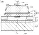
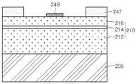
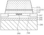
도 12를 참조하면, 제5 실시예에 따른 발광 소자(200)는 전도성 지지부재(240)와, 상기 전도성 지지부재(240) 상에 접합금속층(245)과, 상기 접합금속층(245) 상에 반사층(246)과, 상기 반사층(246) 상에 오믹층(248)과, 상기 반사층(246)의 상면의 둘레 영역에 채널층(247)과, 상기 오믹층(248) 및 상기 채널층(247) 상에 발광구조물(210)과, 상기 발광구조물(210)의 측면에 패시베이션층(235)과, 상기 발광구조물(210)의 상면에 접합층(230)과, 상기 발광구조물(210) 및 상기 접합층(230) 상에 제3 전극(250)을 포함할 수 있다.Referring to FIG. 12, the
상기 전도성 지지부재(240)는 상기 발광 구조물(210)을 지지하며, 상기 제3 전극(250)과 함께 상기 발광 소자(200)에 전원을 제공할 수 있다. 상기 전도성 지지부재(240)는 예를 들어, 구리(Cu), 금(Au), 니켈(Ni), 몰리브덴(Mo), 구리-텅스텐(Cu-W), 캐리어 웨이퍼(예: Si, Ge, GaAs, ZnO, Sic 등) 중 적어도 어느 하나로 형성될 수 있다.The
상기 전도성 지지부재(240) 상에는 상기 접합금속층(245)이 형성될 수 있다. 상기 접합금속층(245)은 상기 전도성 지지부재(240)와 상기 반사층(246) 사이의 계면 접합력을 향상시키기 위해 접착력이 좋은 금속 재질로 형성될 수 있다. 예를 들어, 상기 접합금속층(245)은 Ti, Au, Sn, Ni, Cr, Ga, In, Bi, Cu, Ag 또는 Ta 중 적어도 하나를 포함하여 단층 또는 다층 구조로 형성될 수 있다. 다만, 상기 전도성 지지부재(240)를 본딩 방식이 아니라, 도금 또는 증착 방식에 의해 형성하는 경우, 상기 접합금속층(245)은 형성되지 않을 수도 있다.The
상기 접합금속층(245) 상에는 상기 반사층(246)이 형성될 수 있다. 상기 반사층(246)은 상기 발광구조물(210)로부터 입사되는 빛을 위로 반사시킴으로써 상기 발광 소자(200)의 발광 효율을 향상시킬 수 있다. 상기 반사층(246)은 예를 들어, 은(Ag), 알루미늄(Al), 팔라듐(Pd), 구리(Cu) 또는 백금(Pt) 중 적어도 하나를 포함하는 금속 또는 합금으로 형성될 수 있다.The
상기 반사층(246) 상에는 오믹층(248)이 형성될 수 있다. 상기 오믹층(248)은 상기 반사층(246)과 상기 발광구조물(210) 사이의 오믹 접촉을 형성하기 위해 형성될 수 있다.An
상기 오믹층(248)은 투광성 전도층과 금속을 선택적으로 사용할 수 있으며, ITO(indium tin oxide), IZO(indium zinc oxide), IZTO(indium zinc tin oxide), IAZO(indium aluminum zinc oxide), IGZO(indium gallium zinc oxide), IGTO(indium gallium tin oxide), AZO(aluminum zinc oxide), ATO(antimony tin oxide), GZO(gallium zinc oxide), IrOx, RuOx, Ni, Ag 또는 Au 중 하나 이상을 이용하여 단층 또는 다층으로 구현할 수 있다.The
상기 반사층(246) 상면의 둘레 영역에는 상기 채널층(247)이 형성될 수 있다. 즉, 상기 채널층(247)은 상기 발광구조물(210)과 상기 전도성 지지부재(240) 사이의 둘레 영역에 형성될 수 있다.The
상기 채널층(247)은 상기 전도성 지지부재(240)와 상기 발광구조물(210)이 서로 전기적으로 쇼트되는 것을 방지하며, 제조 공정의 신뢰성을 향상시킬 수 있다.The
상기 채널층(247)은 예를 들어, 전기 절연성을 갖는 재질 또는 상기 발광구조물(210)에 비해 낮은 전기 전도성을 갖는 재질로 형성될 수 있다. 예를 들어, 상기 채널층(247)은 Si02, SixOy, Si3N4, SixNy, SiOxNy, Al2O3, TiO2, ITO, AZO, ZnO 등으로 이루어진 군에서 적어도 하나가 선택되어 형성될 수 있다.The
한편, 상기 오믹층(248)과 상기 발광구조물(210) 사이에는 상기 제3 전극(250)과 적어도 일부가 수직 방향으로 중첩되도록 전류차단층(249)이 형성될 수도 있다. 상기 전류차단층(249)은 상기 제3 전극(250)과 상기 전도성 지지부재(240) 사이의 최단 거리로 전류가 편중되는 것을 방지할 수 있다.Meanwhile, a
상기 전류차단층(249)은 전기 절연성을 갖거나, 상기 제2 도전형 반도체층(216)과 쇼트키 접촉을 형성하는 물질을 이용하여 형성될 수 있으며, 예를 들어, ZnO, SiO2, SiOx, SiOxNy,Si3N4, Al2O3 ,TiOx, Ti, Al, Cr 중 적어도 하나를 포함할 수 있다.The
상기 오믹층(248) 및 상기 채널층(247) 상에는 상기 발광구조물(210)이 형성될 수 있다. 상기 발광구조물(210)은 제2 도전형 반도체층(216), 상기 제2 도전형 반도체층(216) 상에 활성층(214), 상기 활성층(214) 상에 제1 도전형 반도체층(212)을 포함할 수 있으나, 이에 대해 한정하지는 않는다.The
상기 발광구조물(210)은 3족 내지 5족 화합물 반도체로 형성될 수 있으며, 전자 및 정공의 재결합 과정을 거쳐 빛을 생성할 수 있다. 이에 대한 자세한 내용은 앞에서 설명했으므로 생략한다.The
또한, 상기 발광구조물(210) 상면에는 러프니스이 형성될 수 있다. 상기 러프니스은 습식 식각에 의해 형성된 랜덤한 러프니스(roughness)이거나, 패터닝 공정을 통해 형성된 광 결정 구조(photonic crystal)과 같은 주기적인 패턴일 수 있다.In addition, roughness may be formed on an upper surface of the
상기 러프니스은 상기 발광 소자(200)의 광 추출 효율을 향상시킬 뿐 아니라, 상기 발광 구조물(210)과 상기 접합층(230) 사이의 계면의 표면적을 넓힘으로써 둘 사이의 접합력을 향상시킬 수 있다.The roughness may not only improve the light extraction efficiency of the
상기 발광구조물(210)의 측면에는 상기 패시베이션층(235)이 형성될 수 있다. 상기 패시베이션층(235)은 상기 발광구조물(210)이 외부 전극 등과 전기적으로 쇼트되는 것을 방지할 수 있으며, 예를 들어, SiO2, SiOx, SiOxNy,Si3N4, Al2O3로 형성될수 있으나, 이에 대해 한정하지는 않는다.The
상기 발광구조물(210)의 상면의 적어도 일부 영역에는 상기 접합층(230)이 형성될 수 있다. 도 12에 도시된 것처럼, 상기 접합층(230)은 상기 제1 도전형 반도체층(212)의 상면의 일부가 노출되도록 형성될 수 있다.The
상기 접합층(230)은 상기 제1 도전형 반도체층(212)과 상기 제3 전극(250) 사이의 접합력을 향상시켜 궁극적으로는 상기 발광 소자(200)의 신뢰성을 향상시키는 효과를 가질 수 있다.The
이러한 효과는 상기 제1 도전형 반도체층(212)과 상기 제3 전극(250) 사이의 접합력보다, 상기 제3 전극(250)과 상기 접합층(230) 사이의 접합력 및 상기 접합층(230)과 상기 제1 도전형 반도체층(212) 사이의 접합력이 더 크기 때문에 나타날 수 있다.This effect is greater than the bonding force between the first conductivity-
이러한 효과를 극대화하기 위해서는 상기 제3 전극(250)과 상기 접합층(230)의 적어도 일부분이 수직 방향으로 중첩되도록 형성되는 것이 바람직하다. 구체적으로는, 상기 제3 전극(250)과 상기 접합층(230)이 수직 방향으로 중첩되는 영역의 너비는 상기 제3 전극(250) 상면의 전체 너비의 5~90% 범위로 형성될 수 있다. 또는 상기 제3전극(250과 상기 제1도전형 반도체층(112)의 접촉 계면의 면적은 상기 제1 전극 상면의 면적의 5~90%로 형성될 수 있다. 반대로, 상기 제3 전극(250)의 하면 중 상기 제1도전형 반도체층(112)에 접촉되는 면적은 상기 제3 전극(250)의 상면 면적에 비해 10~95% 범위로 형성될 수 있다.In order to maximize such an effect, it is preferable that at least a portion of the
또한, 상기 접합층(230)이 상기 제3 전극(250)과 상기 제1 도전형 반도체층(212) 사이를 더욱 견고히 접합할 수 있도록 상기 접합층(230)에 요철 또는 러프니스를 형성하여 상기 접합층(230)의 표면적을 크게 할 수도 있다.In addition, the unevenness or roughness may be formed in the
상기 접합층(230)의 재질은 예를 들어, SiO2, SiOx, SiOxNy,Si3N4, TiO2, Al2O3, ITO(indium tin oxide), IZO(indium zinc oxide), IZTO(indium zinc tin oxide), IAZO(indium aluminum zinc oxide), IGZO(indium gallium zinc oxide), IGTO(indium gallium tin oxide), AZO(aluminum zinc oxide), ATO(antimony tin oxide), GZO(gallium zinc oxide), IrOx 또는 RuOx 중 적어도 하나로 단층 또는 다층 구조를 가지도록 형성될 수 있으나, 이에 대해 한정하지는 않는다.The material of the
한편, 상기 접합층(230)의 재질은 상기 패시베이션층(235)의 재질과 상이하거나 동일할 수 있다. 또한, 제조 공정에 따라 상기 접합층(230)과 상기 패시베이션층(235)은 일체로 동시에 형성될 수도 있다.Meanwhile, the material of the
또한, 상기 접합층(230)은 광 추출 효율 개선을 위해 상기 발광구조물(210)보다 낮은 굴절률을 갖는 재질로 형성되는 것이 바람직하다.In addition, the
상기 제1 도전형 반도체층(212) 및 상기 접합층(230) 상에는 상기 제3 전극(250)이 형성될 수 있다. 즉, 상기 제3 전극(250)의 하면은 상기 접합층(230)의 상면 및 측면을 둘러싸면서 접촉하고, 상기 제1 도전형 반도체층(212)의 상면과도 접촉할 수 있다. 이에 따라, 상기 제3 전극(250)은 상기 발광구조물(210) 상에 견고히 접합될 수 있게 된다.The
이하, 제5 실시예에 따른 발광 소자(200)의 제조방법에 대해 설명한다. 다만, 앞에서 설명한 내용과 중복되는 설명은 생략하거나 간략히 설명한다.Hereinafter, a method of manufacturing the
도 13 내지 도 20은 제5 실시예에 따른 발광 소자(200)의 제조방법을 설명하는 도면이다.13 to 20 illustrate a method of manufacturing the
도 13을 참조하면, 성장기판(205) 상에 상기 발광구조물(210)을 형성할 수 있다. 상기 발광구조물(210)은 적어도 제1 도전형 반도체층(212), 활성층(214) 및 제2 도전형 반도체층(216)을 포함할 수 있다.Referring to FIG. 13, the
도 14를 참조하면, 상기 발광구조물(210)의 제2 도전형 반도체층(216) 상에 상기 채널층(247) 및 상기 전류차단층(249)을 형성할 수 있다.Referring to FIG. 14, the
상기 채널층(247)은 마스크 패턴을 이용하여 개별 칩(1 chip)의 경계 영역에 형성될 수 있으며, 링 형상, 루프 형상, 프레임 형상 등으로 형성될 수 있다. 상기 채널층(247)은 예를 들어, 전자빔(E-beam) 증착, 스퍼터링(Sputtering), PECVD(Plasma Enhanced Chemical Vapor Deposition) 중 어느 하나의 방법에 의해 형성될 수 있다.The
상기 전류차단층(249)은 후에 형성될 상기 제3 전극(250)과 수직 방향으로 적어도 일부가 중첩되도록 형성될 수 있으며, 증착 또는 도금 방식에 의해 형성될 수 있다.The
도 15를 참조하면, 상기 제2 도전형 반도체층(216) 및 상기 전류차단층(249) 상에 상기 오믹층(248)을 형성하고, 상기 오믹층(248) 및 상기 채널층(247) 상에 상기 반사층(246)을 형성하고, 상기 반사층(246) 상에 상기 접합금속층(245)을 형성하고, 상기 접합금속층(245) 상에 상기 전도성 지지부재(240)를 형성할 수 있다.Referring to FIG. 15, the
상기 오믹층(248) 및 반사층(246)은 증착 또는 도금 방식에 의해 형성될 수 있다.The
상기 전도성 지지부재(240)는 증착 또는 도금 방식에 의해 형성되거나, 별도의 시트로 준비되어 본딩 방식으로 형성될 수 있다. 이때, 상기 전도성 지지부재(240)가 증착 또는 도금 방식에 의해 형성되는 경우, 상기 접합금속층(245)은 형성되지 않을 수도 있다.The
도 16을 참조하면, 상기 성장기판(205)을 제거할 수 있다. 상기 성장기판(205)은 상기 성장기판(110)은 레이저 리프트 오프(Laser Lift Off) 또는 화학적 에칭(Chemical Lift Off) 중 적어도 하나의 방법에 의해 제거될 수 있다.Referring to FIG. 16, the
상기 레이저 리프트 오프(LLO)는 상기 성장기판(205)의 배면을 통해 레이저를 조사함으로써 상기 성장기판(205)과 상기 제1 도전형 반도체층(212) 사이의 계면을 박리시키는 공정이다.The laser lift-off LLO is a process of peeling an interface between the
상기 성장기판(205)이 제거됨에 따라, 상기 제1 도전형 반도체층(212)의 하면이 노출될 수 있다. 이때, 노출된 상기 제1 도전형 반도체층(212)에는 습식 식각을 실시하여 표면 불순물을 제거할 수 있다.As the
도 17을 참조하면, 상기 발광구조물(210)의 칩 경계 영역에 아이솔레이션 에칭을 실시하여 복수개의 발광 소자를 개별 발광 소자 단위로 구분할 수 있다.Referring to FIG. 17, an isolation etching may be performed on a chip boundary region of the
상기 아이솔레이션 에칭(Isolation Etching)은 예를 들어, ICP(Inductively Coupled Plasma)와 같은 건식 식각 방법에 의해 실시될 수 있다.The isolation etching may be performed by a dry etching method such as, for example, an inductively coupled plasma (ICP).
도 18을 참조하면, 상기 발광구조물(210)의 적어도 측면에 상기 패시베이션층(235)을 형성할 수 있다.Referring to FIG. 18, the
구체적으로는, 상기 패시베이션층(235)은 일단이 상기 발광구조물(210)의 상면에 배치되고, 타단이 상기 발광구조물(210)의 측면을 따라 상기 채널층(247) 상에 배치되도록 형성될 수 있으나, 이에 대해 한정하지는 않는다.Specifically, the
상기 패시베이션층(235)은 전자빔 증착, PECVD 또는 스퍼터링 중 적어도 하나의 증착 방식에 의해 형성될 수 있다.The
도 19를 참조하면, 상기 발광구조물(210) 상면에 상기 접합층(230)을 형성할 수 있다.Referring to FIG. 19, the
상기 접합층(230)은 전자빔 증착, PECVD 또는 스퍼터링 중 적어도 하나의 증착 방식에 의해 형성될 수 있으며, 상기 패시베이션층(235)과 동일한 재질로 형성되거나 상이한 재질로 형성될 수 있다.The
이때, 상기 접합층(230)을 형성하기 전에 상기 발광구조물(210)의 상면에 상기 러프니스 또는 패턴을 형성할 수도 있다.In this case, the roughness or the pattern may be formed on the upper surface of the
도 20을 참조하면, 상기 발광구조물(210)의 제1 도전형 반도체층(212) 및 상기 접합층(230) 상에 상기 제3 전극(250)을 형성함으로써, 제5 실시예에 따른 발광 소자(200)를 제공할 수 있다.Referring to FIG. 20, the light emitting device according to the fifth embodiment is formed by forming the
상기 제3 전극(250)의 하면은 상기 접합층(230)의 상면 및 측면에 접촉하므로, 더욱 견고히 상기 발광구조물(210) 상에 접합될 수 있다.
Since the lower surface of the
<발광 소자 패키지><Light Emitting Device Package>
도 21은 실시예에 따른 발광 소자를 포함하는 발광 소자 패키지의 단면도이다.21 is a cross-sectional view of a light emitting device package including a light emitting device according to the embodiment.
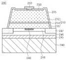
도 21을 참조하면, 실시예에 따른 발광 소자 패키지는 몸체(20)와, 상기 몸체(20)에 설치된 제1 전극층(31) 및 제2 전극층(32)과, 상기 몸체(20)에 설치되어 상기 제1 전극층(31) 및 제2 전극층(32)과 전기적으로 연결되는 실시예에 따른 발광 소자(100)와, 상기 발광 소자(100)를 포위하는 몰딩부재(40)를 포함한다.Referring to FIG. 21, the light emitting device package according to the embodiment is installed on the
상기 몸체(20)는 실리콘 재질, 합성수지 재질, 또는 금속 재질을 포함하여 형성될 수 있으며, 상기 발광 소자(100)의 주위에 경사면이 형성될 수 있다.The
상기 제1 전극층(31) 및 제2 전극층(32)은 서로 전기적으로 분리되며, 상기 발광 소자(100)에 전원을 제공한다. 또한, 상기 제1 전극층(31) 및 제2 전극층(32)은 상기 발광 소자(100)에서 발생된 빛을 반사시켜 광 효율을 증가시킬 수 있으며, 상기 발광 소자(100)에서 발생된 열을 외부로 배출시키는 역할을 할 수도 있다.The
상기 발광 소자(100)는 상기 몸체(20) 상에 설치되거나 상기 제1 전극층(31) 또는 제2 전극층(32) 상에 설치될 수 있다.The
상기 발광 소자(100)는 상기 제1 전극층(31) 및 제2 전극층(32)과 와이어 방식, 플립칩 방식 또는 다이 본딩 방식 중 어느 하나에 의해 전기적으로 연결될 수도 있다.The
상기 몰딩부재(40)는 상기 발광 소자(100)를 포위하여 상기 발광 소자(100)를 보호할 수 있다. 또한, 상기 몰딩부재(40)에는 형광체가 포함되어 상기 발광 소자(100)에서 방출된 광의 파장을 변화시킬 수 있다.The
상기 발광 소자 패키지는 상기에 개시된 실시 예들의 발광 소자 중 적어도 하나를 하나 또는 복수개로 탑재할 수 있으며, 이에 대해 한정하지는 않는다.The light emitting device package may mount at least one of the light emitting devices of the above-described embodiments as one or more, but is not limited thereto.
실시 예에 따른 발광 소자 또는 발광 소자 패키지는 복수개가 기판 상에 어레이되며, 상기 발광 소자 패키지의 광 경로 상에 광학 부재인 도광판, 프리즘 시트, 확산 시트 등이 배치될 수 있다. 이러한 발광 소자 패키지, 기판, 광학 부재는 라이트 유닛으로 기능할 수 있다. 또 다른 실시 예는 상술한 실시 예들에 기재된 반도체 발광소자 또는 발광 소자 패키지를 포함하는 표시 장치, 지시 장치, 조명 시스템으로 구현될 수 있으며, 예를 들어, 조명 시스템은 램프, 가로등, 전광판, 전조등 등과 같은 시스템을 포함할 수 있다.A plurality of light emitting devices or light emitting device packages according to the embodiment may be arranged on a substrate, and a light guide plate, a prism sheet, a diffusion sheet, or the like, which is an optical member, may be disposed on an optical path of the light emitting device package. The light emitting device package, the substrate, and the optical member may function as a light unit. Another embodiment may be implemented as a display device, an indicator device, a lighting system including the semiconductor light emitting device or the light emitting device package described in the above-described embodiments, for example, the lighting system is a lamp, a street lamp, a sign, a headlamp, etc. It may include the same system.
이상에서 실시예들에 설명된 특징, 구조, 효과 등은 본 발명의 적어도 하나의 실시예에 포함되며, 반드시 하나의 실시예에만 한정되는 것은 아니다. 나아가, 각 실시예에서 예시된 특징, 구조, 효과 등은 실시예들이 속하는 분야의 통상의 지식을 가지는 자에 의해 다른 실시예들에 대해서도 조합 또는 변형되어 실시 가능하다. 따라서 이러한 조합과 변형에 관계된 내용들은 본 발명의 범위에 포함되는 것으로 해석되어야 할 것이다.Features, structures, effects, and the like described in the above embodiments are included in at least one embodiment of the present invention, and are not necessarily limited to only one embodiment. Furthermore, the features, structures, effects, and the like illustrated in the embodiments may be combined or modified with respect to other embodiments by those skilled in the art to which the embodiments belong. Therefore, it should be understood that the present invention is not limited to these combinations and modifications.
또한, 이상에서 실시예를 중심으로 설명하였으나 이는 단지 예시일 뿐 본 발명을 한정하는 것이 아니며, 본 발명이 속하는 분야의 통상의 지식을 가진 자라면 본 실시예의 본질적인 특성을 벗어나지 않는 범위에서 이상에 예시되지 않은 여러 가지의 변형과 응용이 가능함을 알 수 있을 것이다. 예를 들어, 실시예에 구체적으로 나타난 각 구성 요소는 변형하여 실시할 수 있는 것이다. 그리고 이러한 변형과 응용에 관계된 차이점들은 첨부된 청구 범위에서 규정하는 본 발명의 범위에 포함되는 것으로 해석되어야 할 것이다.In addition, the above description has been made with reference to the embodiment, which is merely an example, and is not intended to limit the present invention. Those skilled in the art to which the present invention pertains will be illustrated as above without departing from the essential characteristics of the present embodiment. It will be appreciated that various modifications and applications are possible. For example, each component specifically shown in the embodiment can be modified. And differences relating to such modifications and applications will have to be construed as being included in the scope of the invention defined in the appended claims.
100,200: 발광 소자, 105: 성장기판, 112: 제1도전형 반도체층, 114: 활성층, 116: 제2도전형 반도체층, 110: 발광 구조물, 150: 제1전극, 130: 접합층, 120: 투광성전극층, 140: 제2전극100, 200: light emitting device, 105: growth substrate, 112: first conductive semiconductor layer, 114: active layer, 116: second conductive semiconductor layer, 110: light emitting structure, 150: first electrode, 130: bonding layer, 120: Transmissive electrode layer, 140: Second electrode
Claims (30)
Translated fromKorean상기 제1 도전형 반도체층의 상면에 접촉된 접합층;
상기 제1 도전형 반도체층 및 상기 접합층의 상면에 접촉된 제1 전극; 및
상기 제2 도전형 반도체층에 전기적으로 연결된 제2 전극을 포함하고,
상기 제1 전극에 접촉된 접합층은 상기 제2 전극과 이격되는 발광 소자.A light emitting structure including a first conductive semiconductor layer, an active layer on the first conductive semiconductor layer, and a second conductive semiconductor layer on the active layer active layer;
A bonding layer in contact with an upper surface of the first conductivity type semiconductor layer;
A first electrode in contact with an upper surface of the first conductive semiconductor layer and the bonding layer; And
A second electrode electrically connected to the second conductivity type semiconductor layer,
The bonding layer in contact with the first electrode is spaced apart from the second electrode.
상기 접합층은 투광성의 전도물질 및 투광성의 절연물질 중 적어도 하나를 포함하는 발광 소자.The method of claim 1,
The bonding layer includes at least one of a light transmissive conductive material and a light transmissive insulating material.
상기 접합층의 표면에 요철 또는 러프니스를 포함하는 발광 소자.The method of claim 1,
A light emitting device comprising irregularities or roughness on the surface of the bonding layer.
상기 전도성 지지부재 위에 제1 도전형 반도체층, 활성층 및 제2 도전형 반도체층을 포함하는 발광구조물;
상기 발광구조물의 상면의 상면에 접촉된 접합층; 및
상기 발광구조물 및 상기 접합층의 상면에 접촉된 전극을 포함하는 발광 소자.Conductive support members;
A light emitting structure including a first conductive semiconductor layer, an active layer, and a second conductive semiconductor layer on the conductive support member;
A bonding layer in contact with an upper surface of the upper surface of the light emitting structure; And
Light emitting device comprising an electrode in contact with the upper surface of the light emitting structure and the bonding layer.
상기 전극과 상기 접합층의 접촉 계면은 상기 전극의 상면 면적의 5~90%인 발광 소자.16. The method of claim 15,
The contact interface between the electrode and the bonding layer is 5 to 90% of the upper surface area of the electrode.
상기 접합층은 상기 패시베이션층으로부터 연장되어 배치되는 발광 소자.The method of claim 15, further comprising a passivation layer around the light emitting structure,
And the bonding layer extends from the passivation layer.
상기 몸체 위에 적어도 하나의 전극층;
상기 전극층에 전기적으로 연결된 발광 소자; 및
상기 발광 소자 위에 몰딩 부재를 포함하며,
상기 발광 소자는 상기 제1항 내지 제29항 중 어느 한 항의 발광 소자를 포함하는 발광소자 패키지.Body;
At least one electrode layer on the body;
A light emitting device electrically connected to the electrode layer; And
A molding member on the light emitting device,
The light emitting device package comprising a light emitting device of any one of claims 1 to 29.
Priority Applications (16)
| Application Number | Priority Date | Filing Date | Title |
|---|---|---|---|
| KR1020100022754AKR101081135B1 (en) | 2010-03-15 | 2010-03-15 | Light emitting device, method for fabricating the light emitting device and light emitting device package |
| TW100100468ATWI608634B (en) | 2010-03-15 | 2011-01-06 | Illuminating device |
| US13/014,390US8847268B2 (en) | 2010-03-15 | 2011-01-26 | Light emitting device and light emitting device package |
| EP20110153745EP2367210A3 (en) | 2010-03-15 | 2011-02-08 | Light emitting device and light emitting device package |
| CN201610006429.0ACN105470363B (en) | 2010-03-15 | 2011-02-16 | Luminescent device and light emitting device package |
| CN201110040319.3ACN102194958B (en) | 2010-03-15 | 2011-02-16 | Light emitting device and light emitting device package |
| JP2011055810AJP2011192999A (en) | 2010-03-15 | 2011-03-14 | Light-emitting device |
| US14/055,675US8791494B2 (en) | 2010-03-15 | 2013-10-16 | Light emitting device and light emitting device package |
| US14/457,384US9076930B2 (en) | 2010-03-15 | 2014-08-12 | Light emitting device and light emitting device package |
| US14/717,464US9287457B2 (en) | 2010-03-15 | 2015-05-20 | Light emitting device and light emitting device package |
| JP2015178849AJP2016026390A (en) | 2010-03-15 | 2015-09-10 | Light emitting element |
| US15/044,627US9577150B2 (en) | 2010-03-15 | 2016-02-16 | Light emitting device and light emitting device package |
| US15/402,491US9837581B2 (en) | 2010-03-15 | 2017-01-10 | Light emitting device and light emitting device package |
| US15/804,021US10084116B2 (en) | 2010-03-15 | 2017-11-06 | Light emitting device and light emitting device package |
| US15/999,016US10510929B2 (en) | 2010-03-15 | 2018-08-20 | Light emitting device and light emitting device package |
| US16/655,774US10833226B2 (en) | 2010-03-15 | 2019-10-17 | Light emitting device and light emitting device package |
Applications Claiming Priority (1)
| Application Number | Priority Date | Filing Date | Title |
|---|---|---|---|
| KR1020100022754AKR101081135B1 (en) | 2010-03-15 | 2010-03-15 | Light emitting device, method for fabricating the light emitting device and light emitting device package |
Publications (2)
| Publication Number | Publication Date |
|---|---|
| KR20110103608A KR20110103608A (en) | 2011-09-21 |
| KR101081135B1true KR101081135B1 (en) | 2011-11-07 |
Family
ID=44077898
Family Applications (1)
| Application Number | Title | Priority Date | Filing Date |
|---|---|---|---|
| KR1020100022754AExpired - Fee RelatedKR101081135B1 (en) | 2010-03-15 | 2010-03-15 | Light emitting device, method for fabricating the light emitting device and light emitting device package |
Country Status (6)
| Country | Link |
|---|---|
| US (9) | US8847268B2 (en) |
| EP (1) | EP2367210A3 (en) |
| JP (2) | JP2011192999A (en) |
| KR (1) | KR101081135B1 (en) |
| CN (2) | CN105470363B (en) |
| TW (1) | TWI608634B (en) |
Families Citing this family (44)
| Publication number | Priority date | Publication date | Assignee | Title |
|---|---|---|---|---|
| TWI440210B (en) | 2007-01-22 | 2014-06-01 | Cree Inc | Illumination device using external interconnection array of light-emitting device and manufacturing method thereof |
| KR101081135B1 (en) | 2010-03-15 | 2011-11-07 | 엘지이노텍 주식회사 | Light emitting device, method for fabricating the light emitting device and light emitting device package |
| JP2011233783A (en)* | 2010-04-28 | 2011-11-17 | Mitsubishi Heavy Ind Ltd | Semiconductor light-emitting device, protection film thereof, and its manufacturing method |
| KR101735670B1 (en)* | 2010-07-13 | 2017-05-15 | 엘지이노텍 주식회사 | A light emitting device |
| DE102011011140A1 (en) | 2011-02-14 | 2012-08-16 | Osram Opto Semiconductors Gmbh | Optoelectronic semiconductor chip and method for producing optoelectronic semiconductor chips |
| TWI453968B (en)* | 2011-05-20 | 2014-09-21 | Huga Optotech Inc | Semiconductor light emitting structure |
| US9269878B2 (en)* | 2011-05-27 | 2016-02-23 | Lg Innotek Co., Ltd. | Light emitting device and light emitting apparatus |
| KR101248624B1 (en)* | 2011-08-01 | 2013-03-28 | 주식회사 케이이씨 | Light emitting semiconductor device and manufacturing method thereof |
| KR101959036B1 (en)* | 2012-05-17 | 2019-03-18 | 서울바이오시스 주식회사 | Light Emitting Diode having Improved Tolerance against ElectroStatic Discharge and Method for Fabricating the Same |
| WO2013169032A1 (en)* | 2012-05-09 | 2013-11-14 | 서울옵토디바이스주식회사 | Light-emitting diodes having improved light extraction efficiency |
| KR20130128841A (en) | 2012-05-18 | 2013-11-27 | 삼성전자주식회사 | Semiconductor light emitting device having a multi-cell array and manufacturing method for the same, light emitting module and illumination apparatus |
| US11792898B2 (en) | 2012-07-01 | 2023-10-17 | Ideal Industries Lighting Llc | Enhanced fixtures for area lighting |
| US11160148B2 (en) | 2017-06-13 | 2021-10-26 | Ideal Industries Lighting Llc | Adaptive area lamp |
| WO2014021854A1 (en)* | 2012-07-31 | 2014-02-06 | Hewlett-Packard Development Company, L.P. | Thin film stack |
| CN103681723A (en)* | 2012-08-30 | 2014-03-26 | 旭明光电股份有限公司 | Light emitting diode |
| CN103681725A (en)* | 2012-09-11 | 2014-03-26 | 旭明光电股份有限公司 | led |
| CN102867898A (en)* | 2012-10-13 | 2013-01-09 | 江苏新广联科技股份有限公司 | Light-emitting diode chip structure |
| JP6068165B2 (en)* | 2013-01-29 | 2017-01-25 | スタンレー電気株式会社 | Semiconductor optical device and method of manufacturing semiconductor optical device |
| KR20140100115A (en)* | 2013-02-05 | 2014-08-14 | 삼성전자주식회사 | Semiconductor light emitting device |
| KR20140148098A (en)* | 2013-06-21 | 2014-12-31 | 서울바이오시스 주식회사 | Light emitting diode chip |
| KR101650009B1 (en) | 2015-01-15 | 2016-08-22 | 박진상 | The method and the recording media for original image restoration technology based on scattering noise removal and photon detection for single recorded image |
| JP6582738B2 (en)* | 2015-08-26 | 2019-10-02 | 日亜化学工業株式会社 | Light emitting element and light emitting device |
| JP2017054901A (en)* | 2015-09-09 | 2017-03-16 | 豊田合成株式会社 | Group III nitride semiconductor light emitting device and method of manufacturing the same |
| US9705035B1 (en)* | 2015-12-30 | 2017-07-11 | Epistar Corporation | Light emitting device |
| KR102512027B1 (en)* | 2016-03-08 | 2023-03-21 | 엘지이노텍 주식회사 | Semiconductor device, display panel, display device, method of fabricating display panel |
| DE102016105056A1 (en)* | 2016-03-18 | 2017-09-21 | Osram Opto Semiconductors Gmbh | Method for producing an optoelectronic semiconductor chip and optoelectronic semiconductor chip |
| US10529696B2 (en) | 2016-04-12 | 2020-01-07 | Cree, Inc. | High density pixelated LED and devices and methods thereof |
| KR102519668B1 (en)* | 2016-06-21 | 2023-04-07 | 삼성전자주식회사 | Semiconductor light-emitting device and method for manufacturing the same |
| KR102532743B1 (en)* | 2016-12-06 | 2023-05-16 | 쑤저우 레킨 세미컨덕터 컴퍼니 리미티드 | light emitting element |
| KR102613238B1 (en)* | 2017-01-10 | 2023-12-13 | 삼성전자주식회사 | Semiconductor light emitting device and method of manufacturing the same |
| DE102017101877B4 (en) | 2017-01-31 | 2022-02-03 | OSRAM Opto Semiconductors Gesellschaft mit beschränkter Haftung | Single photon source, method of manufacturing a single photon source and method for the controlled generation of photons |
| US10734363B2 (en) | 2017-08-03 | 2020-08-04 | Cree, Inc. | High density pixelated-LED chips and chip array devices |
| JP7290001B2 (en) | 2017-08-03 | 2023-06-13 | クリーエルイーディー・インコーポレーテッド | High-density pixelated LED chips, chip array devices, and methods of making same |
| DE102017119773A1 (en)* | 2017-08-29 | 2019-02-28 | Osram Opto Semiconductors Gmbh | Method for sampling semiconductor chips and semiconductor chip |
| US10529773B2 (en) | 2018-02-14 | 2020-01-07 | Cree, Inc. | Solid state lighting devices with opposing emission directions |
| KR102147443B1 (en)* | 2018-10-25 | 2020-08-28 | 엘지전자 주식회사 | Display device using semiconductor light emitting device and method for manufacturing the same |
| US10903265B2 (en) | 2018-12-21 | 2021-01-26 | Cree, Inc. | Pixelated-LED chips and chip array devices, and fabrication methods |
| CN111033737B (en)* | 2019-03-25 | 2024-02-06 | 湖北三安光电有限公司 | Microluminescent component, microluminescent diode and microluminescent diode transfer method |
| WO2020203729A1 (en)* | 2019-03-29 | 2020-10-08 | 株式会社ジャパンディスプレイ | Method for manufacturing inorganic light-emitting body |
| JP7071648B2 (en) | 2019-05-16 | 2022-05-19 | 日亜化学工業株式会社 | Light emitting device and manufacturing method of light emitting device |
| WO2021087109A1 (en) | 2019-10-29 | 2021-05-06 | Cree, Inc. | Texturing for high density pixelated-led chips |
| US11437548B2 (en) | 2020-10-23 | 2022-09-06 | Creeled, Inc. | Pixelated-LED chips with inter-pixel underfill materials, and fabrication methods |
| CN112510127B (en)* | 2020-12-21 | 2022-04-05 | 厦门大学 | Manufacturing method of suspension LED device |
| CN113990848B (en)* | 2021-10-09 | 2025-04-25 | 武汉华星光电半导体显示技术有限公司 | A display panel |
Citations (2)
| Publication number | Priority date | Publication date | Assignee | Title |
|---|---|---|---|---|
| JP2005019945A (en) | 2003-06-24 | 2005-01-20 | Samsung Electro Mech Co Ltd | Method for manufacturing gallium nitride based semiconductor light emitting device |
| KR100721515B1 (en)* | 2006-01-09 | 2007-05-23 | 서울옵토디바이스주식회사 | Light Emitting Diode Having ITO Layer And Manufacturing Method Thereof |
Family Cites Families (44)
| Publication number | Priority date | Publication date | Assignee | Title |
|---|---|---|---|---|
| JPH04172515A (en) | 1990-11-06 | 1992-06-19 | Matsushita Electric Ind Co Ltd | data reading device |
| JP2697572B2 (en) | 1993-09-21 | 1998-01-14 | 日亜化学工業株式会社 | Gallium nitride based compound semiconductor light emitting device |
| EP0622858B2 (en)* | 1993-04-28 | 2004-09-29 | Nichia Corporation | Gallium nitride-based III-V group compound semiconductor device and method of producing the same |
| US6005258A (en)* | 1994-03-22 | 1999-12-21 | Toyoda Gosei Co., Ltd. | Light-emitting semiconductor device using group III Nitrogen compound having emission layer doped with donor and acceptor impurities |
| JPH09232632A (en)* | 1995-12-22 | 1997-09-05 | Toshiba Corp | Semiconductor light emitting device and method of manufacturing the same |
| US6677619B1 (en) | 1997-01-09 | 2004-01-13 | Nichia Chemical Industries, Ltd. | Nitride semiconductor device |
| JP3916011B2 (en) | 1997-02-21 | 2007-05-16 | シャープ株式会社 | Gallium nitride compound semiconductor light emitting device and method for manufacturing the same |
| JP3342336B2 (en) | 1997-02-25 | 2002-11-05 | 三洋電機株式会社 | Semiconductor light emitting device |
| JP3698229B2 (en)* | 1997-10-24 | 2005-09-21 | ソニー株式会社 | Semiconductor device and semiconductor light emitting device |
| US5952681A (en)* | 1997-11-24 | 1999-09-14 | Chen; Hsing | Light emitting diode emitting red, green and blue light |
| JP3449535B2 (en)* | 1999-04-22 | 2003-09-22 | ソニー株式会社 | Method for manufacturing semiconductor device |
| JP3723434B2 (en) | 1999-09-24 | 2005-12-07 | 三洋電機株式会社 | Semiconductor light emitting device |
| JP2001339121A (en)* | 2000-05-29 | 2001-12-07 | Sharp Corp | Nitride semiconductor light emitting device and optical device including the same |
| US6586762B2 (en)* | 2000-07-07 | 2003-07-01 | Nichia Corporation | Nitride semiconductor device with improved lifetime and high output power |
| US6459098B1 (en)* | 2000-07-26 | 2002-10-01 | Axt, Inc. | Window for light emitting diode |
| JP4619512B2 (en)* | 2000-09-29 | 2011-01-26 | スタンレー電気株式会社 | Optical semiconductor device |
| US20030189215A1 (en)* | 2002-04-09 | 2003-10-09 | Jong-Lam Lee | Method of fabricating vertical structure leds |
| JP2006237574A (en) | 2005-01-31 | 2006-09-07 | Mitsubishi Cable Ind Ltd | GaN-BASED LIGHT EMITTING DIODE |
| JPWO2006082687A1 (en)* | 2005-02-07 | 2008-06-26 | 三菱電線工業株式会社 | GaN-based light emitting diode and light emitting device |
| KR100609968B1 (en) | 2005-06-29 | 2006-08-08 | 엘지전자 주식회사 | Light-emitting diode having electrostatic protection function and manufacturing method thereof |
| JP2007096116A (en)* | 2005-09-29 | 2007-04-12 | Toyoda Gosei Co Ltd | Light emitting element |
| TWI331406B (en)* | 2005-12-14 | 2010-10-01 | Advanced Optoelectronic Tech | Single chip with multi-led |
| CN101820043A (en)* | 2006-01-09 | 2010-09-01 | 首尔Opto仪器股份有限公司 | Light-emitting device |
| US20080121907A1 (en)* | 2006-08-08 | 2008-05-29 | Way-Jze Wen | Light emitting diode and fabricating method thereof |
| JP4172515B2 (en)* | 2006-10-18 | 2008-10-29 | ソニー株式会社 | Method for manufacturing light emitting device |
| KR100809227B1 (en)* | 2006-10-27 | 2008-03-05 | 삼성전기주식회사 | Nitride semiconductor light emitting device and manufacturing method |
| JP5114947B2 (en)* | 2006-12-28 | 2013-01-09 | 富士通株式会社 | Nitride semiconductor device and manufacturing method thereof |
| CN102779918B (en) | 2007-02-01 | 2015-09-02 | 日亚化学工业株式会社 | Semiconductor light-emitting elements |
| KR101239857B1 (en) | 2007-03-07 | 2013-03-06 | 서울옵토디바이스주식회사 | Semiconductor light emitting device and method for manufacturing thereof |
| KR20080087251A (en) | 2007-03-26 | 2008-10-01 | 서울옵토디바이스주식회사 | Light Emitting Diodes With Capacitors |
| KR20090027329A (en) | 2007-09-12 | 2009-03-17 | 삼성전기주식회사 | Vertical structure semiconductor light emitting device and its manufacturing method |
| TWI369009B (en)* | 2007-09-21 | 2012-07-21 | Nat Univ Chung Hsing | Light-emitting chip device with high thermal conductivity |
| JP2009094107A (en)* | 2007-10-03 | 2009-04-30 | Mitsubishi Chemicals Corp | Electrode for GaN-based LED element and GaN-based LED element using the same |
| KR101393353B1 (en)* | 2007-10-29 | 2014-05-13 | 서울바이오시스 주식회사 | Light emitting diode |
| TW200945631A (en)* | 2007-12-28 | 2009-11-01 | Nichia Corp | Semiconductor light emitting element and method for manufacturing the same |
| KR100946102B1 (en) | 2008-03-31 | 2010-03-10 | 삼성전기주식회사 | Nitride Semiconductor Light Emitting Device |
| KR101449030B1 (en)* | 2008-04-05 | 2014-10-08 | 엘지이노텍 주식회사 | group 3 nitride-based semiconductor light emitting diodes and methods to fabricate them |
| KR101449035B1 (en)* | 2008-04-30 | 2014-10-08 | 엘지이노텍 주식회사 | Semiconductor light emitting device |
| KR100986518B1 (en)* | 2008-06-16 | 2010-10-07 | 엘지이노텍 주식회사 | Semiconductor light emitting device |
| US20090321775A1 (en)* | 2008-06-26 | 2009-12-31 | Ghulam Hasnain | LED with Reduced Electrode Area |
| US7939839B2 (en)* | 2008-09-11 | 2011-05-10 | Bridgelux, Inc. | Series connected segmented LED |
| KR101625125B1 (en)* | 2009-12-29 | 2016-05-27 | 서울바이오시스 주식회사 | Light emitting diode having electrode extensions |
| KR101081135B1 (en)* | 2010-03-15 | 2011-11-07 | 엘지이노텍 주식회사 | Light emitting device, method for fabricating the light emitting device and light emitting device package |
| JP5644669B2 (en)* | 2011-05-19 | 2014-12-24 | 日亜化学工業株式会社 | Manufacturing method of nitride semiconductor light emitting device |
- 2010
- 2010-03-15KRKR1020100022754Apatent/KR101081135B1/ennot_activeExpired - Fee Related
- 2011
- 2011-01-06TWTW100100468Apatent/TWI608634B/enactive
- 2011-01-26USUS13/014,390patent/US8847268B2/enactiveActive
- 2011-02-08EPEP20110153745patent/EP2367210A3/ennot_activeCeased
- 2011-02-16CNCN201610006429.0Apatent/CN105470363B/enactiveActive
- 2011-02-16CNCN201110040319.3Apatent/CN102194958B/enactiveActive
- 2011-03-14JPJP2011055810Apatent/JP2011192999A/enactivePending
- 2013
- 2013-10-16USUS14/055,675patent/US8791494B2/enactiveActive
- 2014
- 2014-08-12USUS14/457,384patent/US9076930B2/enactiveActive
- 2015
- 2015-05-20USUS14/717,464patent/US9287457B2/enactiveActive
- 2015-09-10JPJP2015178849Apatent/JP2016026390A/enactivePending
- 2016
- 2016-02-16USUS15/044,627patent/US9577150B2/enactiveActive
- 2017
- 2017-01-10USUS15/402,491patent/US9837581B2/enactiveActive
- 2017-11-06USUS15/804,021patent/US10084116B2/enactiveActive
- 2018
- 2018-08-20USUS15/999,016patent/US10510929B2/enactiveActive
- 2019
- 2019-10-17USUS16/655,774patent/US10833226B2/enactiveActive
Patent Citations (2)
| Publication number | Priority date | Publication date | Assignee | Title |
|---|---|---|---|---|
| JP2005019945A (en) | 2003-06-24 | 2005-01-20 | Samsung Electro Mech Co Ltd | Method for manufacturing gallium nitride based semiconductor light emitting device |
| KR100721515B1 (en)* | 2006-01-09 | 2007-05-23 | 서울옵토디바이스주식회사 | Light Emitting Diode Having ITO Layer And Manufacturing Method Thereof |
Also Published As
| Publication number | Publication date |
|---|---|
| KR20110103608A (en) | 2011-09-21 |
| CN105470363B (en) | 2018-07-20 |
| US10084116B2 (en) | 2018-09-25 |
| US20170125639A1 (en) | 2017-05-04 |
| US20160172542A1 (en) | 2016-06-16 |
| US8791494B2 (en) | 2014-07-29 |
| US20110220942A1 (en) | 2011-09-15 |
| JP2011192999A (en) | 2011-09-29 |
| US20150287885A1 (en) | 2015-10-08 |
| US9577150B2 (en) | 2017-02-21 |
| CN105470363A (en) | 2016-04-06 |
| CN102194958A (en) | 2011-09-21 |
| US9837581B2 (en) | 2017-12-05 |
| US20200052162A1 (en) | 2020-02-13 |
| US20140346440A1 (en) | 2014-11-27 |
| US10510929B2 (en) | 2019-12-17 |
| CN102194958B (en) | 2016-02-03 |
| US20180062045A1 (en) | 2018-03-01 |
| US9287457B2 (en) | 2016-03-15 |
| US8847268B2 (en) | 2014-09-30 |
| US10833226B2 (en) | 2020-11-10 |
| EP2367210A3 (en) | 2014-12-24 |
| JP2016026390A (en) | 2016-02-12 |
| TW201143146A (en) | 2011-12-01 |
| US9076930B2 (en) | 2015-07-07 |
| EP2367210A2 (en) | 2011-09-21 |
| US20190044030A1 (en) | 2019-02-07 |
| US20140042487A1 (en) | 2014-02-13 |
| TWI608634B (en) | 2017-12-11 |
Similar Documents
| Publication | Publication Date | Title |
|---|---|---|
| KR101081135B1 (en) | Light emitting device, method for fabricating the light emitting device and light emitting device package | |
| KR101014155B1 (en) | Light emitting device, light emitting device manufacturing method and light emitting device package | |
| KR101028277B1 (en) | Light emitting device, light emitting device manufacturing method, light emitting device package and light unit | |
| KR100999733B1 (en) | Light emitting device, light emitting device manufacturing method and light emitting device package | |
| KR101047721B1 (en) | Light emitting device, light emitting device manufacturing method and light emitting device package | |
| JP6199948B2 (en) | Light emitting device, light emitting device package | |
| KR100986318B1 (en) | Semiconductor light emitting device and fabrication method thereof | |
| JP5816243B2 (en) | Light emitting device and light emitting device package | |
| KR101020995B1 (en) | Light emitting device, light emitting device manufacturing method and light emitting device package | |
| KR101154709B1 (en) | Light emitting device, method for fabricating the light emitting device, light emitting device package and lighting system | |
| KR101020974B1 (en) | Light emitting device, light emitting device manufacturing method and light emitting device package | |
| JP5513424B2 (en) | Light emitting element | |
| KR20120037636A (en) | A light emitting device and a light emitting device package | |
| KR102250516B1 (en) | Light emitting device | |
| KR20120039412A (en) | Light emitting device, method for fabricating the light emitting device, light emitting device package and lighting system | |
| KR102164087B1 (en) | Light emitting deviceand light emitting device package thereof | |
| KR101039982B1 (en) | Light emitting device and manufacturing method | |
| KR20120014972A (en) | Light emitting device, light emitting device manufacturing method, light emitting device package, and lighting system | |
| KR101628384B1 (en) | Light emitting device, method for fabricating the light emitting device and light emitting device package | |
| KR102237148B1 (en) | Method of manufacturing light emitting device | |
| KR101745996B1 (en) | Light emitting device | |
| KR20110118333A (en) | Light emitting device, light emitting device manufacturing method, light emitting device package, and lighting system | |
| KR101776302B1 (en) | Light emitting device and light emitting device package | |
| KR20110092728A (en) | Light emitting device, light emitting device manufacturing method and light emitting device package | |
| KR20120022091A (en) | Light emitting device, method for fabricating the light emitting device, light emitting device package and lighting system |
Legal Events
| Date | Code | Title | Description |
|---|---|---|---|
| PA0109 | Patent application | St.27 status event code:A-0-1-A10-A12-nap-PA0109 | |
| A201 | Request for examination | ||
| A302 | Request for accelerated examination | ||
| PA0201 | Request for examination | St.27 status event code:A-1-2-D10-D11-exm-PA0201 | |
| PA0302 | Request for accelerated examination | St.27 status event code:A-1-2-D10-D17-exm-PA0302 St.27 status event code:A-1-2-D10-D16-exm-PA0302 | |
| D13-X000 | Search requested | St.27 status event code:A-1-2-D10-D13-srh-X000 | |
| D14-X000 | Search report completed | St.27 status event code:A-1-2-D10-D14-srh-X000 | |
| E902 | Notification of reason for refusal | ||
| PE0902 | Notice of grounds for rejection | St.27 status event code:A-1-2-D10-D21-exm-PE0902 | |
| P11-X000 | Amendment of application requested | St.27 status event code:A-2-2-P10-P11-nap-X000 | |
| P13-X000 | Application amended | St.27 status event code:A-2-2-P10-P13-nap-X000 | |
| E90F | Notification of reason for final refusal | ||
| PE0902 | Notice of grounds for rejection | St.27 status event code:A-1-2-D10-D21-exm-PE0902 | |
| P11-X000 | Amendment of application requested | St.27 status event code:A-2-2-P10-P11-nap-X000 | |
| P13-X000 | Application amended | St.27 status event code:A-2-2-P10-P13-nap-X000 | |
| E902 | Notification of reason for refusal | ||
| PE0902 | Notice of grounds for rejection | St.27 status event code:A-1-2-D10-D21-exm-PE0902 | |
| P11-X000 | Amendment of application requested | St.27 status event code:A-2-2-P10-P11-nap-X000 | |
| P13-X000 | Application amended | St.27 status event code:A-2-2-P10-P13-nap-X000 | |
| PE0902 | Notice of grounds for rejection | St.27 status event code:A-1-2-D10-D21-exm-PE0902 | |
| PG1501 | Laying open of application | St.27 status event code:A-1-1-Q10-Q12-nap-PG1501 | |
| P11-X000 | Amendment of application requested | St.27 status event code:A-2-2-P10-P11-nap-X000 | |
| P13-X000 | Application amended | St.27 status event code:A-2-2-P10-P13-nap-X000 | |
| E701 | Decision to grant or registration of patent right | ||
| PE0701 | Decision of registration | St.27 status event code:A-1-2-D10-D22-exm-PE0701 | |
| GRNT | Written decision to grant | ||
| PR0701 | Registration of establishment | St.27 status event code:A-2-4-F10-F11-exm-PR0701 | |
| PR1002 | Payment of registration fee | St.27 status event code:A-2-2-U10-U11-oth-PR1002 Fee payment year number:1 | |
| PG1601 | Publication of registration | St.27 status event code:A-4-4-Q10-Q13-nap-PG1601 | |
| FPAY | Annual fee payment | Payment date:20141007 Year of fee payment:4 | |
| PR1001 | Payment of annual fee | St.27 status event code:A-4-4-U10-U11-oth-PR1001 Fee payment year number:4 | |
| PN2301 | Change of applicant | St.27 status event code:A-5-5-R10-R13-asn-PN2301 St.27 status event code:A-5-5-R10-R11-asn-PN2301 | |
| FPAY | Annual fee payment | Payment date:20151005 Year of fee payment:5 | |
| PR1001 | Payment of annual fee | St.27 status event code:A-4-4-U10-U11-oth-PR1001 Fee payment year number:5 | |
| FPAY | Annual fee payment | Payment date:20161006 Year of fee payment:6 | |
| PR1001 | Payment of annual fee | St.27 status event code:A-4-4-U10-U11-oth-PR1001 Fee payment year number:6 | |
| R18-X000 | Changes to party contact information recorded | St.27 status event code:A-5-5-R10-R18-oth-X000 | |
| FPAY | Annual fee payment | Payment date:20171011 Year of fee payment:7 | |
| PR1001 | Payment of annual fee | St.27 status event code:A-4-4-U10-U11-oth-PR1001 Fee payment year number:7 | |
| R18-X000 | Changes to party contact information recorded | St.27 status event code:A-5-5-R10-R18-oth-X000 | |
| FPAY | Annual fee payment | Payment date:20181010 Year of fee payment:8 | |
| PR1001 | Payment of annual fee | St.27 status event code:A-4-4-U10-U11-oth-PR1001 Fee payment year number:8 | |
| PR1001 | Payment of annual fee | St.27 status event code:A-4-4-U10-U11-oth-PR1001 Fee payment year number:9 | |
| R18-X000 | Changes to party contact information recorded | St.27 status event code:A-5-5-R10-R18-oth-X000 | |
| PR1001 | Payment of annual fee | St.27 status event code:A-4-4-U10-U11-oth-PR1001 Fee payment year number:10 | |
| PN2301 | Change of applicant | St.27 status event code:A-5-5-R10-R13-asn-PN2301 St.27 status event code:A-5-5-R10-R11-asn-PN2301 | |
| PN2301 | Change of applicant | St.27 status event code:A-5-5-R10-R11-asn-PN2301 | |
| PN2301 | Change of applicant | St.27 status event code:A-5-5-R10-R14-asn-PN2301 | |
| PR1001 | Payment of annual fee | St.27 status event code:A-4-4-U10-U11-oth-PR1001 Fee payment year number:11 | |
| PR1001 | Payment of annual fee | St.27 status event code:A-4-4-U10-U11-oth-PR1001 Fee payment year number:12 | |
| PR1001 | Payment of annual fee | St.27 status event code:A-4-4-U10-U11-oth-PR1001 Fee payment year number:13 | |
| PC1903 | Unpaid annual fee | St.27 status event code:A-4-4-U10-U13-oth-PC1903 Not in force date:20241102 Payment event data comment text:Termination Category : DEFAULT_OF_REGISTRATION_FEE | |
| P22-X000 | Classification modified | St.27 status event code:A-4-4-P10-P22-nap-X000 | |
| PC1903 | Unpaid annual fee | St.27 status event code:N-4-6-H10-H13-oth-PC1903 Ip right cessation event data comment text:Termination Category : DEFAULT_OF_REGISTRATION_FEE Not in force date:20241102 |