KR101079625B1 - Mask pattern forming method, fine pattern forming method and film forming apparatus - Google Patents
Mask pattern forming method, fine pattern forming method and film forming apparatusDownload PDFInfo
- Publication number
- KR101079625B1 KR101079625B1KR1020090092465AKR20090092465AKR101079625B1KR 101079625 B1KR101079625 B1KR 101079625B1KR 1020090092465 AKR1020090092465 AKR 1020090092465AKR 20090092465 AKR20090092465 AKR 20090092465AKR 101079625 B1KR101079625 B1KR 101079625B1
- Authority
- KR
- South Korea
- Prior art keywords
- film
- forming
- pattern
- resist pattern
- resist
- Prior art date
- Legal status (The legal status is an assumption and is not a legal conclusion. Google has not performed a legal analysis and makes no representation as to the accuracy of the status listed.)
- Active
Links
Images


Classifications
- H—ELECTRICITY
- H01—ELECTRIC ELEMENTS
- H01J—ELECTRIC DISCHARGE TUBES OR DISCHARGE LAMPS
- H01J37/00—Discharge tubes with provision for introducing objects or material to be exposed to the discharge, e.g. for the purpose of examination or processing thereof
- H01J37/32—Gas-filled discharge tubes
- H01J37/32009—Arrangements for generation of plasma specially adapted for examination or treatment of objects, e.g. plasma sources
- H01J37/32082—Radio frequency generated discharge
- H01J37/32091—Radio frequency generated discharge the radio frequency energy being capacitively coupled to the plasma
- C—CHEMISTRY; METALLURGY
- C23—COATING METALLIC MATERIAL; COATING MATERIAL WITH METALLIC MATERIAL; CHEMICAL SURFACE TREATMENT; DIFFUSION TREATMENT OF METALLIC MATERIAL; COATING BY VACUUM EVAPORATION, BY SPUTTERING, BY ION IMPLANTATION OR BY CHEMICAL VAPOUR DEPOSITION, IN GENERAL; INHIBITING CORROSION OF METALLIC MATERIAL OR INCRUSTATION IN GENERAL
- C23C—COATING METALLIC MATERIAL; COATING MATERIAL WITH METALLIC MATERIAL; SURFACE TREATMENT OF METALLIC MATERIAL BY DIFFUSION INTO THE SURFACE, BY CHEMICAL CONVERSION OR SUBSTITUTION; COATING BY VACUUM EVAPORATION, BY SPUTTERING, BY ION IMPLANTATION OR BY CHEMICAL VAPOUR DEPOSITION, IN GENERAL
- C23C16/00—Chemical coating by decomposition of gaseous compounds, without leaving reaction products of surface material in the coating, i.e. chemical vapour deposition [CVD] processes
- C23C16/02—Pretreatment of the material to be coated
- C—CHEMISTRY; METALLURGY
- C23—COATING METALLIC MATERIAL; COATING MATERIAL WITH METALLIC MATERIAL; CHEMICAL SURFACE TREATMENT; DIFFUSION TREATMENT OF METALLIC MATERIAL; COATING BY VACUUM EVAPORATION, BY SPUTTERING, BY ION IMPLANTATION OR BY CHEMICAL VAPOUR DEPOSITION, IN GENERAL; INHIBITING CORROSION OF METALLIC MATERIAL OR INCRUSTATION IN GENERAL
- C23C—COATING METALLIC MATERIAL; COATING MATERIAL WITH METALLIC MATERIAL; SURFACE TREATMENT OF METALLIC MATERIAL BY DIFFUSION INTO THE SURFACE, BY CHEMICAL CONVERSION OR SUBSTITUTION; COATING BY VACUUM EVAPORATION, BY SPUTTERING, BY ION IMPLANTATION OR BY CHEMICAL VAPOUR DEPOSITION, IN GENERAL
- C23C16/00—Chemical coating by decomposition of gaseous compounds, without leaving reaction products of surface material in the coating, i.e. chemical vapour deposition [CVD] processes
- C23C16/22—Chemical coating by decomposition of gaseous compounds, without leaving reaction products of surface material in the coating, i.e. chemical vapour deposition [CVD] processes characterised by the deposition of inorganic material, other than metallic material
- C23C16/30—Deposition of compounds, mixtures or solid solutions, e.g. borides, carbides, nitrides
- C23C16/40—Oxides
- C23C16/401—Oxides containing silicon
- C23C16/402—Silicon dioxide
- C—CHEMISTRY; METALLURGY
- C23—COATING METALLIC MATERIAL; COATING MATERIAL WITH METALLIC MATERIAL; CHEMICAL SURFACE TREATMENT; DIFFUSION TREATMENT OF METALLIC MATERIAL; COATING BY VACUUM EVAPORATION, BY SPUTTERING, BY ION IMPLANTATION OR BY CHEMICAL VAPOUR DEPOSITION, IN GENERAL; INHIBITING CORROSION OF METALLIC MATERIAL OR INCRUSTATION IN GENERAL
- C23C—COATING METALLIC MATERIAL; COATING MATERIAL WITH METALLIC MATERIAL; SURFACE TREATMENT OF METALLIC MATERIAL BY DIFFUSION INTO THE SURFACE, BY CHEMICAL CONVERSION OR SUBSTITUTION; COATING BY VACUUM EVAPORATION, BY SPUTTERING, BY ION IMPLANTATION OR BY CHEMICAL VAPOUR DEPOSITION, IN GENERAL
- C23C16/00—Chemical coating by decomposition of gaseous compounds, without leaving reaction products of surface material in the coating, i.e. chemical vapour deposition [CVD] processes
- C23C16/22—Chemical coating by decomposition of gaseous compounds, without leaving reaction products of surface material in the coating, i.e. chemical vapour deposition [CVD] processes characterised by the deposition of inorganic material, other than metallic material
- C23C16/30—Deposition of compounds, mixtures or solid solutions, e.g. borides, carbides, nitrides
- C23C16/40—Oxides
- C23C16/403—Oxides of aluminium, magnesium or beryllium
- C—CHEMISTRY; METALLURGY
- C23—COATING METALLIC MATERIAL; COATING MATERIAL WITH METALLIC MATERIAL; CHEMICAL SURFACE TREATMENT; DIFFUSION TREATMENT OF METALLIC MATERIAL; COATING BY VACUUM EVAPORATION, BY SPUTTERING, BY ION IMPLANTATION OR BY CHEMICAL VAPOUR DEPOSITION, IN GENERAL; INHIBITING CORROSION OF METALLIC MATERIAL OR INCRUSTATION IN GENERAL
- C23C—COATING METALLIC MATERIAL; COATING MATERIAL WITH METALLIC MATERIAL; SURFACE TREATMENT OF METALLIC MATERIAL BY DIFFUSION INTO THE SURFACE, BY CHEMICAL CONVERSION OR SUBSTITUTION; COATING BY VACUUM EVAPORATION, BY SPUTTERING, BY ION IMPLANTATION OR BY CHEMICAL VAPOUR DEPOSITION, IN GENERAL
- C23C16/00—Chemical coating by decomposition of gaseous compounds, without leaving reaction products of surface material in the coating, i.e. chemical vapour deposition [CVD] processes
- C23C16/44—Chemical coating by decomposition of gaseous compounds, without leaving reaction products of surface material in the coating, i.e. chemical vapour deposition [CVD] processes characterised by the method of coating
- C23C16/455—Chemical coating by decomposition of gaseous compounds, without leaving reaction products of surface material in the coating, i.e. chemical vapour deposition [CVD] processes characterised by the method of coating characterised by the method used for introducing gases into reaction chamber or for modifying gas flows in reaction chamber
- C23C16/45523—Pulsed gas flow or change of composition over time
- C23C16/45525—Atomic layer deposition [ALD]
- C23C16/45527—Atomic layer deposition [ALD] characterized by the ALD cycle, e.g. different flows or temperatures during half-reactions, unusual pulsing sequence, use of precursor mixtures or auxiliary reactants or activations
- C23C16/45536—Use of plasma, radiation or electromagnetic fields
- G—PHYSICS
- G03—PHOTOGRAPHY; CINEMATOGRAPHY; ANALOGOUS TECHNIQUES USING WAVES OTHER THAN OPTICAL WAVES; ELECTROGRAPHY; HOLOGRAPHY
- G03F—PHOTOMECHANICAL PRODUCTION OF TEXTURED OR PATTERNED SURFACES, e.g. FOR PRINTING, FOR PROCESSING OF SEMICONDUCTOR DEVICES; MATERIALS THEREFOR; ORIGINALS THEREFOR; APPARATUS SPECIALLY ADAPTED THEREFOR
- G03F7/00—Photomechanical, e.g. photolithographic, production of textured or patterned surfaces, e.g. printing surfaces; Materials therefor, e.g. comprising photoresists; Apparatus specially adapted therefor
- G03F7/26—Processing photosensitive materials; Apparatus therefor
- G03F7/40—Treatment after imagewise removal, e.g. baking
- H—ELECTRICITY
- H01—ELECTRIC ELEMENTS
- H01J—ELECTRIC DISCHARGE TUBES OR DISCHARGE LAMPS
- H01J37/00—Discharge tubes with provision for introducing objects or material to be exposed to the discharge, e.g. for the purpose of examination or processing thereof
- H01J37/32—Gas-filled discharge tubes
- H01J37/32431—Constructional details of the reactor
- H01J37/3244—Gas supply means
- H—ELECTRICITY
- H01—ELECTRIC ELEMENTS
- H01J—ELECTRIC DISCHARGE TUBES OR DISCHARGE LAMPS
- H01J37/00—Discharge tubes with provision for introducing objects or material to be exposed to the discharge, e.g. for the purpose of examination or processing thereof
- H01J37/32—Gas-filled discharge tubes
- H01J37/32431—Constructional details of the reactor
- H01J37/32798—Further details of plasma apparatus not provided for in groups H01J37/3244 - H01J37/32788; special provisions for cleaning or maintenance of the apparatus
- H01J37/32816—Pressure
- H01J37/32834—Exhausting
- H—ELECTRICITY
- H01—ELECTRIC ELEMENTS
- H01L—SEMICONDUCTOR DEVICES NOT COVERED BY CLASS H10
- H01L21/00—Processes or apparatus adapted for the manufacture or treatment of semiconductor or solid state devices or of parts thereof
- H01L21/02—Manufacture or treatment of semiconductor devices or of parts thereof
- H01L21/027—Making masks on semiconductor bodies for further photolithographic processing not provided for in group H01L21/18 or H01L21/34
- H01L21/0271—Making masks on semiconductor bodies for further photolithographic processing not provided for in group H01L21/18 or H01L21/34 comprising organic layers
- H01L21/0273—Making masks on semiconductor bodies for further photolithographic processing not provided for in group H01L21/18 or H01L21/34 comprising organic layers characterised by the treatment of photoresist layers
- H01L21/0274—Photolithographic processes
- H—ELECTRICITY
- H01—ELECTRIC ELEMENTS
- H01L—SEMICONDUCTOR DEVICES NOT COVERED BY CLASS H10
- H01L21/00—Processes or apparatus adapted for the manufacture or treatment of semiconductor or solid state devices or of parts thereof
- H01L21/02—Manufacture or treatment of semiconductor devices or of parts thereof
- H01L21/027—Making masks on semiconductor bodies for further photolithographic processing not provided for in group H01L21/18 or H01L21/34
- H01L21/033—Making masks on semiconductor bodies for further photolithographic processing not provided for in group H01L21/18 or H01L21/34 comprising inorganic layers
- H01L21/0334—Making masks on semiconductor bodies for further photolithographic processing not provided for in group H01L21/18 or H01L21/34 comprising inorganic layers characterised by their size, orientation, disposition, behaviour, shape, in horizontal or vertical plane
- H01L21/0337—Making masks on semiconductor bodies for further photolithographic processing not provided for in group H01L21/18 or H01L21/34 comprising inorganic layers characterised by their size, orientation, disposition, behaviour, shape, in horizontal or vertical plane characterised by the process involved to create the mask, e.g. lift-off masks, sidewalls, or to modify the mask, e.g. pre-treatment, post-treatment
- H—ELECTRICITY
- H01—ELECTRIC ELEMENTS
- H01L—SEMICONDUCTOR DEVICES NOT COVERED BY CLASS H10
- H01L21/00—Processes or apparatus adapted for the manufacture or treatment of semiconductor or solid state devices or of parts thereof
- H01L21/02—Manufacture or treatment of semiconductor devices or of parts thereof
- H01L21/027—Making masks on semiconductor bodies for further photolithographic processing not provided for in group H01L21/18 or H01L21/34
- H01L21/033—Making masks on semiconductor bodies for further photolithographic processing not provided for in group H01L21/18 or H01L21/34 comprising inorganic layers
- H01L21/0334—Making masks on semiconductor bodies for further photolithographic processing not provided for in group H01L21/18 or H01L21/34 comprising inorganic layers characterised by their size, orientation, disposition, behaviour, shape, in horizontal or vertical plane
- H01L21/0338—Process specially adapted to improve the resolution of the mask
- H—ELECTRICITY
- H01—ELECTRIC ELEMENTS
- H01L—SEMICONDUCTOR DEVICES NOT COVERED BY CLASS H10
- H01L21/00—Processes or apparatus adapted for the manufacture or treatment of semiconductor or solid state devices or of parts thereof
- H01L21/02—Manufacture or treatment of semiconductor devices or of parts thereof
- H01L21/04—Manufacture or treatment of semiconductor devices or of parts thereof the devices having potential barriers, e.g. a PN junction, depletion layer or carrier concentration layer
- H01L21/18—Manufacture or treatment of semiconductor devices or of parts thereof the devices having potential barriers, e.g. a PN junction, depletion layer or carrier concentration layer the devices having semiconductor bodies comprising elements of Group IV of the Periodic Table or AIIIBV compounds with or without impurities, e.g. doping materials
- H01L21/30—Treatment of semiconductor bodies using processes or apparatus not provided for in groups H01L21/20 - H01L21/26
- H01L21/31—Treatment of semiconductor bodies using processes or apparatus not provided for in groups H01L21/20 - H01L21/26 to form insulating layers thereon, e.g. for masking or by using photolithographic techniques; After treatment of these layers; Selection of materials for these layers
- H01L21/3105—After-treatment
- H01L21/311—Etching the insulating layers by chemical or physical means
- H01L21/31127—Etching organic layers
- H01L21/31133—Etching organic layers by chemical means
- H01L21/31138—Etching organic layers by chemical means by dry-etching
- H—ELECTRICITY
- H01—ELECTRIC ELEMENTS
- H01L—SEMICONDUCTOR DEVICES NOT COVERED BY CLASS H10
- H01L21/00—Processes or apparatus adapted for the manufacture or treatment of semiconductor or solid state devices or of parts thereof
- H01L21/02—Manufacture or treatment of semiconductor devices or of parts thereof
- H01L21/04—Manufacture or treatment of semiconductor devices or of parts thereof the devices having potential barriers, e.g. a PN junction, depletion layer or carrier concentration layer
- H01L21/18—Manufacture or treatment of semiconductor devices or of parts thereof the devices having potential barriers, e.g. a PN junction, depletion layer or carrier concentration layer the devices having semiconductor bodies comprising elements of Group IV of the Periodic Table or AIIIBV compounds with or without impurities, e.g. doping materials
- H01L21/30—Treatment of semiconductor bodies using processes or apparatus not provided for in groups H01L21/20 - H01L21/26
- H01L21/31—Treatment of semiconductor bodies using processes or apparatus not provided for in groups H01L21/20 - H01L21/26 to form insulating layers thereon, e.g. for masking or by using photolithographic techniques; After treatment of these layers; Selection of materials for these layers
- H01L21/3105—After-treatment
- H01L21/311—Etching the insulating layers by chemical or physical means
- H01L21/31144—Etching the insulating layers by chemical or physical means using masks
- H—ELECTRICITY
- H01—ELECTRIC ELEMENTS
- H01L—SEMICONDUCTOR DEVICES NOT COVERED BY CLASS H10
- H01L21/00—Processes or apparatus adapted for the manufacture or treatment of semiconductor or solid state devices or of parts thereof
- H01L21/02—Manufacture or treatment of semiconductor devices or of parts thereof
- H01L21/04—Manufacture or treatment of semiconductor devices or of parts thereof the devices having potential barriers, e.g. a PN junction, depletion layer or carrier concentration layer
- H01L21/18—Manufacture or treatment of semiconductor devices or of parts thereof the devices having potential barriers, e.g. a PN junction, depletion layer or carrier concentration layer the devices having semiconductor bodies comprising elements of Group IV of the Periodic Table or AIIIBV compounds with or without impurities, e.g. doping materials
- H01L21/30—Treatment of semiconductor bodies using processes or apparatus not provided for in groups H01L21/20 - H01L21/26
- H01L21/31—Treatment of semiconductor bodies using processes or apparatus not provided for in groups H01L21/20 - H01L21/26 to form insulating layers thereon, e.g. for masking or by using photolithographic techniques; After treatment of these layers; Selection of materials for these layers
- H01L21/3205—Deposition of non-insulating-, e.g. conductive- or resistive-, layers on insulating layers; After-treatment of these layers
- H01L21/321—After treatment
- H01L21/3213—Physical or chemical etching of the layers, e.g. to produce a patterned layer from a pre-deposited extensive layer
- H01L21/32139—Physical or chemical etching of the layers, e.g. to produce a patterned layer from a pre-deposited extensive layer using masks
- H—ELECTRICITY
- H01—ELECTRIC ELEMENTS
- H01L—SEMICONDUCTOR DEVICES NOT COVERED BY CLASS H10
- H01L21/00—Processes or apparatus adapted for the manufacture or treatment of semiconductor or solid state devices or of parts thereof
- H01L21/70—Manufacture or treatment of devices consisting of a plurality of solid state components formed in or on a common substrate or of parts thereof; Manufacture of integrated circuit devices or of parts thereof
- H01L21/71—Manufacture of specific parts of devices defined in group H01L21/70
- H01L21/768—Applying interconnections to be used for carrying current between separate components within a device comprising conductors and dielectrics
- H01L21/76801—Applying interconnections to be used for carrying current between separate components within a device comprising conductors and dielectrics characterised by the formation and the after-treatment of the dielectrics, e.g. smoothing
- H01L21/76802—Applying interconnections to be used for carrying current between separate components within a device comprising conductors and dielectrics characterised by the formation and the after-treatment of the dielectrics, e.g. smoothing by forming openings in dielectrics
- H01L21/76816—Aspects relating to the layout of the pattern or to the size of vias or trenches
- H—ELECTRICITY
- H01—ELECTRIC ELEMENTS
- H01L—SEMICONDUCTOR DEVICES NOT COVERED BY CLASS H10
- H01L21/00—Processes or apparatus adapted for the manufacture or treatment of semiconductor or solid state devices or of parts thereof
- H01L21/02—Manufacture or treatment of semiconductor devices or of parts thereof
- H01L21/02104—Forming layers
- H01L21/02107—Forming insulating materials on a substrate
- H01L21/02109—Forming insulating materials on a substrate characterised by the type of layer, e.g. type of material, porous/non-porous, pre-cursors, mixtures or laminates
- H01L21/02112—Forming insulating materials on a substrate characterised by the type of layer, e.g. type of material, porous/non-porous, pre-cursors, mixtures or laminates characterised by the material of the layer
- H01L21/02123—Forming insulating materials on a substrate characterised by the type of layer, e.g. type of material, porous/non-porous, pre-cursors, mixtures or laminates characterised by the material of the layer the material containing silicon
- H01L21/02164—Forming insulating materials on a substrate characterised by the type of layer, e.g. type of material, porous/non-porous, pre-cursors, mixtures or laminates characterised by the material of the layer the material containing silicon the material being a silicon oxide, e.g. SiO2
- H—ELECTRICITY
- H01—ELECTRIC ELEMENTS
- H01L—SEMICONDUCTOR DEVICES NOT COVERED BY CLASS H10
- H01L21/00—Processes or apparatus adapted for the manufacture or treatment of semiconductor or solid state devices or of parts thereof
- H01L21/02—Manufacture or treatment of semiconductor devices or of parts thereof
- H01L21/02104—Forming layers
- H01L21/02107—Forming insulating materials on a substrate
- H01L21/02109—Forming insulating materials on a substrate characterised by the type of layer, e.g. type of material, porous/non-porous, pre-cursors, mixtures or laminates
- H01L21/02112—Forming insulating materials on a substrate characterised by the type of layer, e.g. type of material, porous/non-porous, pre-cursors, mixtures or laminates characterised by the material of the layer
- H01L21/02172—Forming insulating materials on a substrate characterised by the type of layer, e.g. type of material, porous/non-porous, pre-cursors, mixtures or laminates characterised by the material of the layer the material containing at least one metal element, e.g. metal oxides, metal nitrides, metal oxynitrides or metal carbides
- H01L21/02175—Forming insulating materials on a substrate characterised by the type of layer, e.g. type of material, porous/non-porous, pre-cursors, mixtures or laminates characterised by the material of the layer the material containing at least one metal element, e.g. metal oxides, metal nitrides, metal oxynitrides or metal carbides characterised by the metal
- H01L21/02178—Forming insulating materials on a substrate characterised by the type of layer, e.g. type of material, porous/non-porous, pre-cursors, mixtures or laminates characterised by the material of the layer the material containing at least one metal element, e.g. metal oxides, metal nitrides, metal oxynitrides or metal carbides characterised by the metal the material containing aluminium, e.g. Al2O3
- H—ELECTRICITY
- H01—ELECTRIC ELEMENTS
- H01L—SEMICONDUCTOR DEVICES NOT COVERED BY CLASS H10
- H01L21/00—Processes or apparatus adapted for the manufacture or treatment of semiconductor or solid state devices or of parts thereof
- H01L21/02—Manufacture or treatment of semiconductor devices or of parts thereof
- H01L21/02104—Forming layers
- H01L21/02107—Forming insulating materials on a substrate
- H01L21/02109—Forming insulating materials on a substrate characterised by the type of layer, e.g. type of material, porous/non-porous, pre-cursors, mixtures or laminates
- H01L21/02205—Forming insulating materials on a substrate characterised by the type of layer, e.g. type of material, porous/non-porous, pre-cursors, mixtures or laminates the layer being characterised by the precursor material for deposition
- H01L21/02208—Forming insulating materials on a substrate characterised by the type of layer, e.g. type of material, porous/non-porous, pre-cursors, mixtures or laminates the layer being characterised by the precursor material for deposition the precursor containing a compound comprising Si
- H01L21/02219—Forming insulating materials on a substrate characterised by the type of layer, e.g. type of material, porous/non-porous, pre-cursors, mixtures or laminates the layer being characterised by the precursor material for deposition the precursor containing a compound comprising Si the compound comprising silicon and nitrogen
- H—ELECTRICITY
- H01—ELECTRIC ELEMENTS
- H01L—SEMICONDUCTOR DEVICES NOT COVERED BY CLASS H10
- H01L21/00—Processes or apparatus adapted for the manufacture or treatment of semiconductor or solid state devices or of parts thereof
- H01L21/02—Manufacture or treatment of semiconductor devices or of parts thereof
- H01L21/02104—Forming layers
- H01L21/02107—Forming insulating materials on a substrate
- H01L21/02225—Forming insulating materials on a substrate characterised by the process for the formation of the insulating layer
- H01L21/0226—Forming insulating materials on a substrate characterised by the process for the formation of the insulating layer formation by a deposition process
- H01L21/02263—Forming insulating materials on a substrate characterised by the process for the formation of the insulating layer formation by a deposition process deposition from the gas or vapour phase
- H01L21/02271—Forming insulating materials on a substrate characterised by the process for the formation of the insulating layer formation by a deposition process deposition from the gas or vapour phase deposition by decomposition or reaction of gaseous or vapour phase compounds, i.e. chemical vapour deposition
- H01L21/02274—Forming insulating materials on a substrate characterised by the process for the formation of the insulating layer formation by a deposition process deposition from the gas or vapour phase deposition by decomposition or reaction of gaseous or vapour phase compounds, i.e. chemical vapour deposition in the presence of a plasma [PECVD]
- H—ELECTRICITY
- H01—ELECTRIC ELEMENTS
- H01L—SEMICONDUCTOR DEVICES NOT COVERED BY CLASS H10
- H01L21/00—Processes or apparatus adapted for the manufacture or treatment of semiconductor or solid state devices or of parts thereof
- H01L21/02—Manufacture or treatment of semiconductor devices or of parts thereof
- H01L21/02104—Forming layers
- H01L21/02107—Forming insulating materials on a substrate
- H01L21/02225—Forming insulating materials on a substrate characterised by the process for the formation of the insulating layer
- H01L21/0226—Forming insulating materials on a substrate characterised by the process for the formation of the insulating layer formation by a deposition process
- H01L21/02263—Forming insulating materials on a substrate characterised by the process for the formation of the insulating layer formation by a deposition process deposition from the gas or vapour phase
- H01L21/02271—Forming insulating materials on a substrate characterised by the process for the formation of the insulating layer formation by a deposition process deposition from the gas or vapour phase deposition by decomposition or reaction of gaseous or vapour phase compounds, i.e. chemical vapour deposition
- H01L21/0228—Forming insulating materials on a substrate characterised by the process for the formation of the insulating layer formation by a deposition process deposition from the gas or vapour phase deposition by decomposition or reaction of gaseous or vapour phase compounds, i.e. chemical vapour deposition deposition by cyclic CVD, e.g. ALD, ALE, pulsed CVD
Landscapes
- Engineering & Computer Science (AREA)
- Chemical & Material Sciences (AREA)
- Physics & Mathematics (AREA)
- General Physics & Mathematics (AREA)
- Manufacturing & Machinery (AREA)
- Power Engineering (AREA)
- Microelectronics & Electronic Packaging (AREA)
- Computer Hardware Design (AREA)
- Condensed Matter Physics & Semiconductors (AREA)
- Chemical Kinetics & Catalysis (AREA)
- General Chemical & Material Sciences (AREA)
- Metallurgy (AREA)
- Organic Chemistry (AREA)
- Mechanical Engineering (AREA)
- Materials Engineering (AREA)
- Inorganic Chemistry (AREA)
- Plasma & Fusion (AREA)
- Analytical Chemistry (AREA)
- Electromagnetism (AREA)
- Drying Of Semiconductors (AREA)
- Formation Of Insulating Films (AREA)
- Photosensitive Polymer And Photoresist Processing (AREA)
- Exposure Of Semiconductors, Excluding Electron Or Ion Beam Exposure (AREA)
- Internal Circuitry In Semiconductor Integrated Circuit Devices (AREA)
Abstract
Translated fromKoreanDescription
Translated fromKorean본 발명은 반도체 프로세스에 이용되는 마스크 패턴의 형성 방법, 미세 패턴의 형성 방법 및 성막 장치에 관한 것으로, 특히 노광 장치의 해상 한계 이하의 패턴을 형성할 때에 제조 프로세스의 비용을 증대시키지 않고 패턴 치수를 보정하는 정밀도를 향상시킬 수 있는 마스크 패턴의 형성 방법, 미세 패턴의 형성 방법 및 성막 장치에 관한 것이다.BACKGROUND OF THE
반도체 디바이스의 고집적화에 수반하여, 제조 프로세스에 요구되는 배선 또는 분리폭은 미세화되고 있다. 일반적으로 미세 패턴은 포토리소그래피 기술을 이용하여 레지스트 패턴을 형성하고, 레지스트 패턴을 에칭 마스크로 이용하여 하지(下地)의 각종 박막을 에칭함으로써 형성된다. 따라서, 미세 패턴을 형성하기 위해서는 포토리소그래피 기술이 중요하지만, 근래의 반도체 디바이스의 미세화는 포토리소그래피 기술의 해상 한계 이하를 요구하기에까지 이르렀다.With high integration of semiconductor devices, the wiring or separation width required for the manufacturing process is miniaturized. In general, the fine pattern is formed by forming a resist pattern using photolithography techniques, and etching various thin films of the base using the resist pattern as an etching mask. Therefore, photolithography technology is important for forming fine patterns, but in recent years, miniaturization of semiconductor devices has come to demand the resolution limit of photolithography technology.
여기서, 박막을 에칭하여 미세 패턴을 형성하기 위한 마스크가 되는 패턴을 마스크 패턴이라고 정의한다. 마스크 패턴은 산화막 등의 희생막 또는 레지스트막으로 이루어지는 경우가 있다. 또한, 이하에서는 미세 패턴이라고 하는 경우에 마스크 패턴의 의미를 포함하는 경우가 있다.Here, the pattern used as the mask for etching a thin film and forming a fine pattern is defined as a mask pattern. The mask pattern may be made of a sacrificial film or resist film such as an oxide film. In addition, below, when called a fine pattern, the meaning of a mask pattern may be included.
이러한 해상 한계 이하의 패턴을 형성하는 기술은, 예를 들면 특허 문헌 1에 기재되어 있다.The technique of forming a pattern below such a resolution limit is described in
특허 문헌 1은, 제 1 감광막 패턴(이하, '제 1 레지스트 패턴'이라고 함)을 형성하고 제 1 레지스트 패턴을 베이킹한 후, 제 1 레지스트 패턴 상에 산화막을 형성한다. 이후, 제 1 레지스트 패턴끼리의 사이에 제 2 감광막 패턴(이하, '제 2 레지스트 패턴'이라고 함)을 형성하고, 제 1 레지스트 패턴 및 제 2 레지스트 패턴을 에칭 마스크로 이용하여, 하지의 박막을 에칭하여 미세 패턴을 형성한다.
특허 문헌 1에 의하면, 2 개의 노광 마스크를 이용하여 미세 패턴을 형성하므로, 1 개의 노광 마스크를 이용하여 미세 패턴을 형성하는 경우에 비해 2 배 이상의 분해능을 얻을 수 있다. 이 때문에, 해상 한계 이하의 미세 패턴을 형성할 수 있다.According to
또한, 패턴 유기막 상에의 실리콘 산화막의 성막 프로세스를 SWT(사이드월 트랜스퍼 프로세스 : Side Wall Transfer Process) 또는 LLE(리소그래피-리소그래피-에칭 : Lithography Lithography Etching) 등의 프로세스와 조합시키는 미세 패턴의 형성 방법이, 상술한 포토리소그래피 기술의 해상 한계 이하의 미세 패턴을 형성하는 기술로서 주목받고 있다.In addition, a method of forming a fine pattern in which a film forming process of a silicon oxide film on a pattern organic film is combined with a process such as SWT (Side Wall Transfer Process) or LLE (Lithography Lithography-Etching: Lithography Lithography Etching). It is attracting attention as a technique of forming the fine pattern below the resolution limit of the photolithography technique mentioned above.
이에 이용되는 레지스트 패턴 상에 산화막을 형성하는 기술은, 예를 들면 특 허 문헌 2에 기재되어 있다.The technique of forming an oxide film on the resist pattern used for this is described in
특허 문헌 2에는, 해상 한계 이하의 미세 패턴을 형성하는 방법은 기재되어 있지 않으나, 레지스트 패턴 상에 산화막을 형성해 둠으로써, 레지스트 패턴의 박형화 현상을 방지할 수 있고, 형성된 미세 패턴에 스트리에이션(striation)이나 위글링(wiggling)이 발생하는 것을 방지할 수 있는 기술이 기재되어 있다.
선행 기술 문헌Prior art literature
특허 문헌 1: 일본특허공보 제2757983호Patent Document 1: Japanese Patent Publication No. 2757983
특허 문헌 2: 일본특허공개공보 2004-080033호Patent Document 2: Japanese Patent Application Laid-Open No. 2004-080033
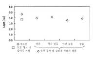
그러나, 상기의 패턴 유기막 상에의 실리콘 산화막의 성막 프로세스를 SWT 또는 LLE 등의 미세 패턴 등에 조합시키는 경우, 다음과 같은 문제가 있었다.However, when combining the film-forming process of the silicon oxide film on the said pattern organic film with fine patterns, such as SWT or LLE, there existed the following problems.
상기한 바와 같이, 리소그래피의 미세화 한계에 의해, 패턴 유기막은 리소그래피 후의 치수 보정(슬리밍, 트리밍, 또는 스무딩) 기술이 필요불가결하지만, 그 공정을 추가함에 따라 비용이 증가한다고 하는 문제가 있었다.As described above, due to the miniaturization limit of lithography, the pattern organic film is indispensable for the dimensional correction (slimming, trimming, or smoothing) technique after lithography, but there is a problem that the cost increases with the addition of the process.
또한, 슬리밍, 트리밍, 또는 스무딩을 행하여 미세 패턴의 패턴 치수의 보정을 행하는 경우에는, 레지스트 도포 장치, 애싱 장치 또는 에칭 장치 등을 이용하여 행해지고, 성막 처리는 성막 장치를 이용하여 행해지고 있다. 이 때문에, 슬리밍 처리를 끝낸 반도체 기판(웨이퍼)은 애싱 장치로부터 일단 인출된 후, 성막 장치로 반송되도록 되어 있다. 그러나, 슬리밍 처리 후에 웨이퍼가 장치로부터 인출되므로, 레지스트 패턴의 표면에 먼지 등이 부착될 가능성이 있다. 레지스트 패턴의 표면에 먼지 등이 부착되면, 레지스트 패턴 상에 형성되는 실리콘 산화막에서는 결함 밀도가 증가하고, 또한 그 막 두께의 균일성이 쉽게 손상된다고 하는 문제가 있었다.In addition, when correcting the pattern size of a fine pattern by slimming, trimming, or smoothing, it is performed using a resist coating apparatus, an ashing apparatus, an etching apparatus, etc., and the film-forming process is performed using the film-forming apparatus. For this reason, the semiconductor substrate (wafer) which finished the slimming process is once taken out from an ashing apparatus, and is conveyed to a film-forming apparatus. However, since the wafer is taken out from the apparatus after the slimming process, there is a possibility that dust or the like adheres to the surface of the resist pattern. If dust or the like adheres to the surface of the resist pattern, there is a problem that the defect density increases in the silicon oxide film formed on the resist pattern and the uniformity of the film thickness is easily damaged.
또한, 슬리밍 처리 또는 성막 처리 시에, 레지스트 패턴의 선단(先端)과 근원 사이의 폭 치수의 차이가 작아지도록 유지하기 어렵고, 형상이 뛰어난 미세 패턴을 형성할 수 없다고 하는 문제가 있었다.In addition, during the slimming process or the film formation process, there is a problem that it is difficult to maintain such that the difference in the width dimension between the tip and the base of the resist pattern is small, and a fine pattern excellent in shape cannot be formed.
본 발명은, 상기의 점을 감안하여 이루어진 것으로, 패턴 유기막에 실리콘 산화막을 성막함으로써, 마스크 패턴 및 미세 패턴을 형성할 때에 레지스트 패턴을 슬리밍 처리하는 처리 장치를 사용하는 공정을 삭감할 수 있고, 마스크 패턴 및 미세 패턴을 형성하는 프로세스의 비용을 저감할 수 있는 마스크 패턴의 형성 방법, 미세 패턴의 형성 방법 및 성막 장치를 제공한다. 또한, 레지스트 패턴의 선단과 근원 사이의 폭 치수의 차이가 작아지도록 유지하면서 슬리밍 처리 또는 성막 처리를 할 수 있고, 형상이 뛰어난 미세 패턴을 형성할 수 있는 마스크 패턴의 형성 방법, 미세 패턴의 형성 방법 및 성막 장치를 제공한다.This invention is made | formed in view of said point, and by forming a silicon oxide film in a pattern organic film, the process of using the processing apparatus which slimming-processes a resist pattern at the time of forming a mask pattern and a fine pattern can be reduced, Provided are a method of forming a mask pattern, a method of forming a fine pattern, and a film forming apparatus capable of reducing the cost of the process of forming the mask pattern and the fine pattern. In addition, a method of forming a mask pattern and a method of forming a fine pattern, which can be slimmed or formed into a film and can form a fine pattern having excellent shape while maintaining the difference in the width dimension between the tip and the base of the resist pattern small. And a film forming apparatus.
상기의 과제를 해결하기 위하여, 본 발명에서는 후술하는 각 수단을 구비한 것을 특징으로 하는 것이다.MEANS TO SOLVE THE PROBLEM In order to solve said subject, this invention is equipped with each means mentioned later. It is characterized by the above-mentioned.
본 발명의 일 실험예에 의하면, 박막 상에 레지스트막을 형성하는 공정과, 포토리소그래피 기술을 이용하여 상기 레지스트막을 소정의 피치를 갖는 레지스트 패턴으로 가공하는 패턴 가공 공정과, 상기 레지스트 패턴의 형상을 가공하는 형상 가공 공정과, 소스 가스와 산소 래디컬 또는 산소 함유 가스를 공급하고 상기 형상 가공 공정에 의해 형상이 가공된 상기 레지스트 패턴 및 상기 박막 상에 산화막을 성막하는 성막 공정을 구비하는 마스크 패턴의 형성 방법으로서, 상기 형상 가공 공정과 상기 성막 공정을, 상기 산화막을 성막하는 성막 장치 내에서 연속하여 행하는 것을 특징으로 하는 마스크 패턴의 형성 방법이 제공된다.According to an experimental example of the present invention, a step of forming a resist film on a thin film, a pattern processing step of processing the resist film into a resist pattern having a predetermined pitch using photolithography technology, and processing the shape of the resist pattern And a film forming step of supplying a source gas, an oxygen radical or an oxygen-containing gas, and a film forming step of forming an oxide film on the resist pattern and the thin film processed by the shape processing step. As a method of forming a mask pattern, the shape processing step and the film forming step are continuously performed in a film forming apparatus for forming the oxide film.
또한, 본 발명의 일 실험예에 의하면, 피에칭막 상에 반사 방지막을 형성하는 공정과, 상기 반사 방지막 상에 레지스트막을 형성하는 공정과, 포토리소그래피 기술을 이용하여 상기 레지스트막을 소정의 피치로 배열하는 라인부를 포함하는 레지스트 패턴으로 가공하는 패턴 가공 공정과, 산화막을 성막하는 성막 장치 내에서 상기 레지스트 패턴의 형상을 가공하는 형상 가공 공정과, 상기 형상 가공 공정과 연속하여, 상기 성막 장치 내에 소스 가스와 산소 래디컬 또는 산소 함유 가스를 공급하고 상기 형상 가공 공정에 의하여 형상이 가공된 상기 레지스트 패턴 및 상기 피에칭막 상에 산화막을 성막하는 성막 공정과, 상기 산화막이, 형상이 가공된 상기 레지스트 패턴의 상기 라인부의 측면에 측벽으로서 잔존하도록 상기 산화막을 에칭하는 에칭 공정과, 형상이 가공된 상기 레지스트 패턴을 제거하고, 측벽으로서 잔존하고 상기 산화막으로 이루어지는 측벽부를 형성하는 공정과, 상기 측벽부를 마스크로서 상기 반사 방지막을 에칭하고, 상기 측벽부 및 상기 반사 방지막으로 이루어지는 마스크 패턴을 형성하는 공정을 구비하는 마스크 패턴의 형성 방법이 제공된다.In addition, according to an experimental example of the present invention, a process of forming an anti-reflection film on an etching target film, a process of forming a resist film on the anti-reflection film, and photoresist technology to arrange the resist film at a predetermined pitch A pattern processing step for processing into a resist pattern including a line portion to be formed; a shape processing step for processing a shape of the resist pattern in a film forming apparatus for forming an oxide film; and a source gas in the film forming apparatus in succession to the shape processing step. And a film forming step of supplying an oxygen radical or an oxygen containing gas to form an oxide film on the resist pattern and the etching target film processed by the shape processing step, and the oxide film of the resist pattern processed into a shape. Etching to etch the oxide film so that it remains as a sidewall on the side of the line portion Removing the resist pattern whose shape and shape have been processed, forming a sidewall portion made of the oxide film remaining as a sidewall, etching the antireflection film using the sidewall portion as a mask, and a mask comprising the sidewall portion and the antireflection film There is provided a method of forming a mask pattern comprising a step of forming a pattern.
또한, 본 발명의 일 실험예에 의하면, 피에칭막 상에 반사 방지막을 형성하는 공정과, 상기 반사 방지막 상에 레지스트막을 형성하는 공정과, 포토리소그래피 기술을 이용하여 상기 레지스트막을 제 1 피치로 배열되는 제 1 레지스트 패턴으로 가공하는 제 1 패턴 가공 공정과, 산화막을 성막하는 성막 장치 내에서 상기 제 1 레지스트 패턴의 형상을 가공하는 제 1 형상 가공 공정과, 상기 제 1 형상 가공 공정과 연속하여, 상기 성막 장치 내로 소스 가스와 산소 래디컬 또는 산소 함유 가스를 공급하고, 상기 제 1 형상 가공 공정에 의하여 형상이 가공된 상기 제 1 레지스트 패턴 및 상기 피에칭막 상에 산화막을 성막하는 성막 공정과, 상기 산화막 상 에 제 2 레지스트막을 형성하는 공정과, 포토리소그래피 기술을 이용하여 상기 제 2 레지스트막을 상기 제 1 피치와 실질적으로 동일한 제 2 피치로 배열하고, 또한 상기 제 1 피치의 실질적으로 절반을 어긋나게 하여 상기 제 1 레지스트 패턴과 교호적으로 배열되는 제 2 레지스트 패턴으로 가공하는 제 2 패턴 가공 공정과, 상기 제 2 레지스트 패턴의 형상을 가공하는 제 2 형상 가공 공정과, 형상이 가공된 상기 제 1 레지스트 패턴 및 형상이 가공된 상기 제 2 레지스트 패턴을 마스크로서 상기 산화막 및 상기 반사 방지막을 에칭하고, 상기 제 1 피치의 실질적으로 절반의 피치로 배열하고, 상기 제 1 레지스트막 및 상기 제 2 레지스트막으로 이루어지는 마스크 패턴을 형성하는 공정을 구비하는 마스크 패턴의 형성 방법이 제공된다.In addition, according to an experimental example of the present invention, a process of forming an anti-reflection film on an etching target film, a process of forming a resist film on the anti-reflection film, and photoresist technology to arrange the resist film at a first pitch In succession with a first pattern processing step for processing into a first resist pattern to be formed, a first shape processing step for processing a shape of the first resist pattern in a film forming apparatus for forming an oxide film, and the first shape processing step, A film forming step of supplying a source gas, an oxygen radical or an oxygen-containing gas into the film forming apparatus, and forming an oxide film on the first resist pattern and the etching target film whose shape is processed by the first shape processing step; Forming a second resist film on the oxide film, and forming the second resist film using the photolithography technique. A second pattern processing step of arranging at a second pitch that is substantially equal to the pitch, and processing a second resist pattern alternately arranged with the first resist pattern by shifting substantially half of the first pitch; Etching the oxide film and the anti-reflection film using a second shape processing step of processing a shape of a second resist pattern, the first resist pattern processed from the shape, and the second resist pattern processed from the shape as a mask; A method of forming a mask pattern is provided, which is arranged at a pitch substantially half of one pitch and includes a step of forming a mask pattern made of the first resist film and the second resist film.
또한, 본 발명의 일 실험예에 의하면, 진공 유지 가능하게 설치되고 반도체 기판을 처리하기 위한 처리 용기와, 상기 처리 용기 내로 소스 가스를 공급하는 소스 가스 공급 수단과, 상기 처리 용기 내로 산소 래디컬 또는 산소 함유 가스를 공급하는 산소 래디컬 공급 수단을 구비하고, 상기 소스 가스 공급 수단과 상기 산소 래디컬 공급 수단이 상기 처리 용기 내로 상기 소스 가스와 상기 산소 래디컬 또는 상기 산소 함유 가스를 교호적으로 공급함으로써, 레지스트 패턴이 형성된 반도체 기판 상에 산화막을 성막하는 성막 장치로서, 상기 레지스트 패턴이 형성된 반도체 기판 상에 상기 산화막을 성막하기 전에, 상기 산소 래디컬 공급 수단이 상기 처리 용기 내로 상기 산소 래디컬을 공급함으로써, 상기 레지스트 패턴의 형상을 가공하는 것을 특징으로 하는 성막 장치가 제공된다.Further, according to an experimental example of the present invention, a processing container for vacuum holding and processing of a semiconductor substrate, source gas supply means for supplying a source gas into the processing container, and oxygen radical or oxygen into the processing container An oxygen radical supply means for supplying a containing gas, wherein the source gas supply means and the oxygen radical supply means alternately supply the source gas and the oxygen radical or the oxygen containing gas into the processing container, thereby providing a resist pattern. A film forming apparatus for forming an oxide film on a formed semiconductor substrate, wherein the oxygen radical supplying means supplies the oxygen radical into the processing container before the oxide film is formed on the semiconductor substrate on which the resist pattern is formed, thereby forming the resist pattern. Characterized by processing the shape of The film forming apparatus is provided.
또한, 본 발명의 일 실험예에 의하면, 반도체 기판 상에 피에칭막을 개재하 여 형성된 반사 방지막과, 상기 반사 방지막 상에 형성된 레지스트 패턴의 측벽을 피복하고 산화막으로 이루어지는 측벽부를 포함하는 마스크 패턴을 형성하기 위하여, 소스 가스와 산소 래디컬 또는 산소 함유 가스를 교호적으로 공급함으로써, 상기 레지스트 패턴이 형성된 상기 반사 방지막 상에 상기 레지스트 패턴을 등방적(等方的)으로 피복하도록 상기 산화막을 성막하는 성막 장치로서, 진공 유지 가능하게 설치되고 반도체 기판을 처리하기 위한 처리 용기와, 상기 처리 용기 내로 상기 소스 가스를 공급하는 소스 가스 공급 수단과, 상기 처리 용기 내로 상기 산소 래디컬 또는 상기 산소 함유 가스를 공급하는 산소 래디컬 공급 수단을 구비하고, 상기 레지스트 패턴이 형성된 반도체 기판 상에 상기 산화막을 성막하기 전에, 상기 산소 래디컬 공급 수단이 상기 처리 용기 내로 상기 산소 래디컬을 공급함으로써, 상기 레지스트 패턴의 형상을 가공하는 것을 특징으로 하는 성막 장치가 제공된다.In addition, according to an experimental example of the present invention, a mask pattern is formed on a semiconductor substrate through an etching target film, and a mask pattern including a sidewall portion formed of an oxide film and covering sidewalls of a resist pattern formed on the antireflection film. In order to do this, a film forming apparatus for forming the oxide film so as to isotropically coat the resist pattern on the antireflection film on which the resist pattern is formed by alternately supplying a source gas and an oxygen radical or an oxygen containing gas. A processing container for vacuum holding and for processing a semiconductor substrate, source gas supply means for supplying the source gas into the processing container, and oxygen for supplying the oxygen radical or the oxygen-containing gas into the processing container; Radial supply means, wherein the resist pattern is Generated before forming the oxide film on the semiconductor substrate, and the oxygen radicals supplying means by supplying the oxygen radical into the processing chamber, a film forming apparatus, characterized in that for machining the shape of the resist pattern is provided.
또한, 본 발명의 일 실험예에 의하면, 반도체 기판 상에 아래로부터 차례로 피에칭막 및 반사 방지막을 개재하여 형성되고, 제 1 피치로 배열되는 제 1 레지스트 패턴과, 상기 제 1 피치와 실질적으로 동일한 제 2 피치로 배열하고, 또한 상기 제 1 피치의 실질적으로 절반을 어긋나게 하여 상기 제 1 레지스트 패턴과 교호적으로 배열하는 제 2 레지스트 패턴을 포함하는 마스크 패턴을 형성하기 위하여, 소스 가스와 산소 래디컬 또는 산소 함유 가스를 교호적으로 공급함으로써, 상기 레지스트 패턴이 형성된 상기 반사 방지막 상에 상기 레지스트 패턴을 등방적으로 피복하도록 상기 산화막을 성막하는 성막 장치로서, 진공 유지 가능하게 설치되고 반 도체 기판을 처리하기 위한 처리 용기와, 상기 처리 용기 내로 상기 소스 가스를 공급하는 소스 가스 공급 수단과, 상기 처리 용기 내로 상기 산소 래디컬 또는 상기 산소 함유 가스를 공급하는 산소 래디컬 공급 수단을 구비하고, 상기 레지스트 패턴이 형성된 반도체 기판 상에 상기 산화막을 성막하기 전에, 상기 산소 래디컬 공급 수단이 상기 처리 용기 내로 상기 산소 래디컬을 공급함으로써, 상기 레지스트 패턴의 형상을 가공하는 것을 특징으로 하는 성막 장치가 제공된다.In addition, according to an experimental example of the present invention, a first resist pattern which is formed on a semiconductor substrate through an etching target film and an anti-reflection film in order from below, and arranged at a first pitch, is substantially the same as the first pitch. Source gas and oxygen radicals or to form a mask pattern comprising a second resist pattern arranged at a second pitch and alternately aligned with the first resist pattern by substantially shifting half of the first pitch; A film forming apparatus for forming an oxide film so as to isotropically coat the resist pattern on the antireflective film on which the resist pattern is formed by alternately supplying an oxygen-containing gas, which is provided so as to be able to hold a vacuum and to process a semiconductor substrate. A processing vessel for supplying the source gas into the processing vessel; Means, and oxygen radical supply means for supplying the oxygen radical or the oxygen-containing gas into the processing container, wherein the oxygen radical supply means performs the processing before depositing the oxide film on the semiconductor substrate on which the resist pattern is formed. The film forming apparatus is provided by processing the shape of the resist pattern by supplying the oxygen radicals into the container.
또한, 본 발명의 일 실험예에 의하면, 피에칭막 상에 반사 방지막을 형성하는 공정과, 상기 반사 방지막 상에 레지스트막을 형성하는 공정과, 포토리소그래피 기술을 이용하여 상기 레지스트막을 제 1 피치로 배열하는 라인부를 포함하는 제 1 레지스트 패턴으로 가공하는 제 1 패턴 가공 공정과, 상기 제 1 레지스트 패턴의 형상을 가공하는 제 1 형상 가공 공정과, 소스 가스와 산소 함유 가스를 공급하고, 상기 제 1 형상 가공 공정에 의해 형상이 가공된 상기 제 1 레지스트 패턴 및 상기 피에칭막 상에 상온에서 알루미늄 산화막을 성막하는 성막 공정을 구비하는 마스크 패턴의 형성 방법이 제공된다.In addition, according to an experimental example of the present invention, a process of forming an anti-reflection film on an etching target film, a process of forming a resist film on the anti-reflection film, and photoresist technology to arrange the resist film at a first pitch A first pattern processing step for processing into a first resist pattern including a line portion to be formed; a first shape processing step for processing a shape of the first resist pattern; and a source gas and an oxygen-containing gas; Provided is a method of forming a mask pattern including a film forming step of forming an aluminum oxide film at room temperature on the first resist pattern whose shape is processed by a processing step and the etching target film.
본 발명에 의하면, 패턴 유기막에 실리콘 산화막을 성막함으로써, 마스크 패턴 및 미세 패턴을 형성할 때에 레지스트 패턴을 슬리밍 처리하는 처리 장치를 사용하는 공정을 삭감할 수 있고, 마스크 패턴 및 미세 패턴을 형성하는 프로세스의 비용을 저감할 수 있다. 또한, 레지스트 패턴의 선단과 근원 사이의 폭 치수의 차이가 작아지도록 유지하면서 슬리밍 처리 또는 성막 처리할 수 있고, 형상이 뛰어 난 마스크 패턴 및 미세 패턴을 형성할 수 있다.According to the present invention, by forming a silicon oxide film on a patterned organic film, the steps of using a processing apparatus for slimming a resist pattern when forming a mask pattern and a fine pattern can be reduced, thereby forming a mask pattern and a fine pattern. The cost of the process can be reduced. In addition, a slimming process or a film forming process can be performed while keeping the difference in the width dimension between the tip and the base of the resist pattern small, and a mask pattern and a fine pattern having excellent shape can be formed.
이어서, 본 발명을 실시하기 위한 형태에 대하여 도면과 함께 설명한다.Next, the form for implementing this invention is demonstrated with drawing.
(제 1 실시예)(First embodiment)
도 1, 도 2a 내지 도 2h, 도 3 내지 도 6, 도 7a 내지 도 7c, 도 8a 내지 도 8d를 참조하여 본 발명의 제 1 실시예에 따른 미세 패턴의 형성 방법 및 성막 장치를 설명한다.A method of forming a fine pattern and a film forming apparatus according to a first embodiment of the present invention will be described with reference to FIGS. 1, 2A to 2H, 3 to 6, 7A to 7C, and 8A to 8D.
먼저, 도 1, 도 2a 내지 도 2h를 참조하여 본 발명의 제 1 실시예에 따른 미세 패턴의 형성 방법을 설명한다.First, a method of forming a fine pattern according to a first embodiment of the present invention will be described with reference to FIGS. 1 and 2A to 2H.
도 1은 본 실시예에 따른 미세 패턴의 형성 방법의 각 공정의 순서를 설명하기 위한 순서도이다. 도 2a 내지 도 2h는 각각 본 실시예에 따른 미세 패턴의 형성 방법을 설명하기 위한 도이며, 각 공정에서의 미세 패턴의 구조를 모식적으로 도시한 단면도이다. 또한, 도 1의 단계(S11) 내지 단계(S17) 및 단계(S18)의 각각의 공정이 행해진 후의 미세 패턴의 구조는, 도 2a 내지 도 2h의 각각의 단면도에서 도시한 구조에 대응된다.1 is a flowchart for explaining the order of each step of the method for forming a fine pattern according to the present embodiment. 2A to 2H are diagrams for explaining the fine pattern formation method according to the present embodiment, respectively, and are sectional views schematically showing the structure of the fine pattern in each step. In addition, the structure of the fine pattern after each process of step S11 to step S17 of FIG. 1 is performed corresponds to the structure shown in each sectional drawing of FIG. 2A-2H.
또한, 상술한 바와 같이, 박막을 에칭하여 미세 패턴을 형성하기 위한 마스크가 되는 패턴을 마스크 패턴이라고 정의한다. 마스크 패턴은 산화막 등의 희생막 또는 레지스트막으로 이루어지는 경우가 있다. 또한, 이하에서는 미세 패턴이라고 하는 경우에 마스크 패턴의 의미를 포함하는 경우가 있다(이하의 실시예에서도 동일함).In addition, as mentioned above, the pattern used as the mask for etching a thin film and forming a fine pattern is defined as a mask pattern. The mask pattern may be made of a sacrificial film or resist film such as an oxide film. In addition, below, the meaning of a mask pattern may be included in the case of a fine pattern (it is the same also in the following example).
본 실시예에 따른 미세 패턴의 형성 방법은, 도 1에 도시한 바와 같이, 박막을 형성하는 공정과, 레지스트막을 형성하는 공정과, 패턴 가공 공정과, 형상 가공 공정과, 성막 공정과, 에칭 공정과, 레지스트 패턴을 제거하고 유기막을 에칭하는 공정을 포함한다. 박막을 형성하는 공정은 단계(S11)의 공정을 포함하고, 레지스트막을 형성하는 공정은 단계(S12)의 공정을 포함하고, 패턴 가공 공정은 단계(S13)의 공정을 포함하고, 레지스트 패턴의 형상을 가공하는 공정은 단계(S14)의 공정을 포함하고, 성막 공정은 단계(S15)의 공정을 포함하고, 에칭 공정은 단계(S16)의 공정을 포함하고, 레지스트 패턴을 제거하고 유기막을 에칭하는 공정은 단계(S17)의 공정을 포함한다.As shown in FIG. 1, the method for forming a fine pattern according to the present embodiment includes a process of forming a thin film, a process of forming a resist film, a pattern processing process, a shape processing process, a film forming process, and an etching process. And removing the resist pattern and etching the organic film. The process of forming the thin film includes the process of step S11, the process of forming the resist film includes the process of step S12, the pattern processing process includes the process of step S13, and the shape of the resist pattern The process of processing the process includes the process of step S14, the film forming process includes the process of step S15, and the etching process includes the process of step S16, removing the resist pattern and etching the organic film. The process includes the process of step S17.
또한, 도 1에 도시한 바와 같이, 단계(S14)와 단계(S15)의 공정은 동일 챔버(처리 용기) 내에서 연속 처리된다.1, the process of step S14 and step S15 is continuously processed in the same chamber (processing container).
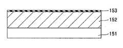
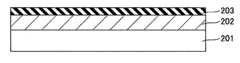
단계(S11)는 반도체 기판 상에 박막을 형성하는 공정이다. 도 2a는 단계(S11)의 공정이 행해진 후의 미세 패턴의 구조를 도시한 단면도이다.Step S11 is a process of forming a thin film on a semiconductor substrate. FIG. 2A is a cross-sectional view showing the structure of the fine pattern after the step S11 is performed.
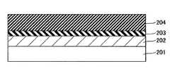
단계(S11)에서는, 도 2a에 도시한 바와 같이, 반도체 기판(101) 상에 아래로부터 차례로 박막(102), 유기막(103)을 형성한다. 박막(102)은 패턴을 형성함으로써 그 후의 여러 가공 공정을 행하는 경우의 마스크로서 기능한다. 유기막(103)은 패턴이 형성되고 박막(102)의 패턴을 형성하기 위한 마스크로서 기능한다. 또한 유기막(103)은 그 위에 형성되는 포토레지스트막(104)의 포토리소그래피를 행할 때의 반사 방지막(BARC : Bottom anti-Reflecting Coating)으로서의 기능을 가지는 경우도 있다.In step S11, as shown in FIG. 2A, the
또한, 반도체 기판(101)은 반도체, 예를 들면 실리콘 기판만을 나타내는 것이 아니라, 반도체 기판 내 또는 반도체 기판 상에 형성된 반도체 소자 또는 집적 회로 패턴에 대응된 도전막, 이들을 절연하는 층간 절연막이 형성된 구조체를 포함한다고 정의한다.In addition, the
또한, 본 실시예에 따른 박막 및 유기막은, 각각 본 발명에서의 피에칭막, 반사 방지막에 상당한다.In addition, the thin film and organic film which concerns on a present Example are corresponded to the etching target film and antireflection film in this invention, respectively.
박막(102)의 재질은 특별히 한정되지 않고, 예를 들면 질화 실리콘, 산화 실리콘, 산질화 실리콘, 비결정 실리콘, 또는 폴리 실리콘을 포함하는 막을 이용할 수 있다. 또한, 박막(102)의 두께는 특별히 한정되지 않고, 예를 들면 20 ~ 200 nm로 할 수 있다.The material of the
유기막(103)의 재질은 특별히 한정되지 않고, 예를 들면 화학 기상법(CVD : Chemical Vapor Deposition)에 의해 성막된 비결정 탄소, 스핀 온에 의해 성막된 폴리페놀 또는 i 선 레지스트 등의 포토레지스트를 포함하는 광범위한 유기계의 재료를 이용할 수 있다. 또한, 유기막(103)의 두께는 특별히 한정되지 않고, 예를 들면 150 ~ 300 nm로 할 수 있다.The material of the
단계(S12)는 포토레지스트막(104)을 성막하는 공정이다. 도 2b는 단계(S12)의 공정이 행해진 후의 미세 패턴의 구조를 도시한 단면도이다.Step S12 is a process of forming a
포토레지스트막(104)의 재질은, 예를 들면 ArF 레지스트를 이용할 수 있다. 또한, 포토레지스트막(104)의 두께는 특별히 한정되지 않고, 예를 들면 50 ~ 200 nm로 할 수 있다.As the material of the
이어서, 단계(S13)를 포함하는 패턴 가공 공정을 행한다. 단계(S13)는 성막된 포토레지스트막(104)을 노광, 현상하여 포토레지스트막(104)으로 이루어지는 레지스트 패턴(104a)을 형성하는 공정이다. 또한, 도 2c는 단계(S13)의 공정이 행해진 후의 미세 패턴의 구조를 도시한 단면도이다.Next, the pattern processing process containing step S13 is performed. Step S13 is a step of forming a resist
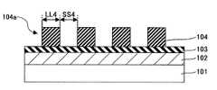
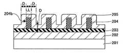
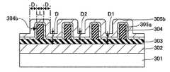
도 2c에 도시한 바와 같이, 포토레지스트막(104)으로 이루어지는 레지스트 패턴(104a)이 형성된다. 레지스트 패턴(104a)은 유기막(103)을 에칭하는 공정에서의 마스크로서 기능한다. 레지스트 패턴(104a)의 라인폭(LL4) 및 스페이스폭(SS4)은 특별히 한정되지 않고, 모두 예를 들면 60nm로 할 수 있다.As shown in Fig. 2C, a resist
또한, 본 실시예에서, 라인폭(LL4)을 가지고 레지스트 패턴을 구성하는 하나 하나의 라인을 라인부라고 정의한다. 따라서, 본 실시예에 따른 패턴 가공 공정은, 포토리소그래피 기술을 이용하여 레지스트막을 소정의 피치로 배열하는 라인부를 포함하는 레지스트 패턴으로 가공하는 공정이다.In addition, in the present embodiment, one line forming the resist pattern with the line width LL4 is defined as the line portion. Therefore, the pattern processing process which concerns on a present Example is a process of processing into the resist pattern containing the line part which arrange | positions a resist film by predetermined pitch using photolithography technique.
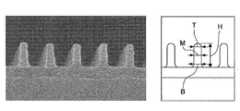
이어서, 단계(S14)를 포함하는 형상 가공 공정을 행한다. 단계(S14)는 포토레지스트막(104)으로 이루어지는 레지스트 패턴(104a)을 슬리밍 처리하여, 포토레지스트막(104)으로 이루어지는 레지스트 패턴(104b)을 형성하는 공정이다. 또한, 도 2d는 단계(S14)의 공정이 행해진 후의 미세 패턴의 구조를 도시한 단면도이다.Next, the shape processing process containing step S14 is performed. Step S14 is a step of slimming the resist
또한, 슬리밍 처리는 본 발명에 있어서의 형상 가공 공정에서의 형상을 가공하는 처리에 상당하며, 트리밍 처리라고도 한다.In addition, the slimming process corresponds to the process which processes the shape in the shape processing process in this invention, and is also called trimming process.
슬리밍 처리의 방법은 특별히 한정되지 않고, 슬리밍 처리 조건의 일례는 산소 래디컬 또는 오존 가스를 포함하는 분위기 중, 온도는 실온 ~ 100℃이다. 또한, 도 2c 및 도 2d에 도시한 바와 같이, 슬리밍 처리되어 생기는 레지스트 패턴(104b)의 라인폭(LL1)은 슬리밍 처리를 행하기 전의 레지스트 패턴(104a)의 라인폭(LL4)에 비해 가늘어지므로, 레지스트 패턴(104b)의 라인폭(LL1) 및 스페이스폭(SS1)과, 레지스트 패턴(104a)의 라인폭(LL4) 및 스페이스폭(SS4)과의 대소 관계는 LL1 < LL4, SS1 > SS4가 된다. LL1 및 SS1의 값은 특별히 한정되지 않고, 예를 들면 LL1을 30 nm, SS1을 90 nm로 할 수 있다.The method of the slimming treatment is not particularly limited, and one example of the slimming treatment condition is a room temperature to 100 ° C in an atmosphere containing oxygen radicals or ozone gas. 2C and 2D, the line width LL1 of the resist
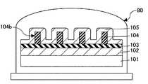
본 실시예에서, 단계(S14)는 그 후 연속하여 행해지는 단계(S15)의 성막 공정을 행하기 위한 성막 장치의 처리 용기 내에서 행해진다.In this embodiment, step S14 is performed in the processing container of the film forming apparatus for performing the film forming process of step S15 subsequently performed.
또한, 단계(S14)를 행하는 경우에는 유기막(반사 방지막)(102)이 에칭되지 않는 조건을 선택하여 행한다. 일례로서, 후술하는 실험예 1과 같은 조건으로 행함으로써 유기막(반사 방지막)(102)이 에칭되지 않도록 할 수 있다. 단계(S14)를 유기막(반사 방지막)(102)이 에칭되는 조건에서 행하는 경우, 유기막(반사 방지막)(102)이 완전히 에칭되지 않고 어중간하게 남게 되어 그 후의 마스크 패턴의 형성 방법을 정밀도 좋게 행할 수 없기 때문이다.In addition, when performing step S14, the conditions which do not etch the organic film (antireflection film) 102 are selected and performed. As an example, the organic film (antireflection film) 102 can be prevented from being etched by performing under the same conditions as in Experimental Example 1 described later. When the step S14 is performed under the condition that the organic film (antireflection film) 102 is etched, the organic film (antireflection film) 102 is not completely etched and remains halfway, so that the method of forming the mask pattern thereafter with high precision is achieved. This is because it cannot be done.
다음에, 단계(S14)에 이어서 성막 장치의 처리 용기 내에서 단계(S15)의 공정을 포함하는 성막 공정을 행한다. 단계(S15)는 슬리밍 처리된 레지스트 패턴(104b) 및 유기막(103) 상에 SiO2막(105)을 성막하는 성막 공정이다. 또한, 도 2e는 단계(S15)의 공정이 행해진 후의 미세 패턴의 구조를 도시한 단면도이다.Next, following the step S14, a film forming step including the step S15 is performed in the processing container of the film forming apparatus. Step S15 is a film forming step of forming a SiO2 film 105 on the slimmed resist
또한, SiO2막(산화 실리콘막)은 본 발명에서의 실리콘 산화막에 상당한다. 또한 이하에서, SiO2막 대신에 SiOx막을 비롯하여 실리콘과 산소를 주성분으로서 포함하는 다른 조성막이어도 좋다. 또한, 산질화 실리콘막(SiON막)을 이용할 수도 있다.Note that the SiO2 film (silicon oxide film) corresponds to the silicon oxide film in the present invention. In addition, instead of the SiO2 film, another composition film containing silicon and oxygen as main components may be used below. In addition, a silicon oxynitride film (SiON film) can also be used.
SiO2막(105)의 성막 공정은 포토레지스트막(104)이 레지스트 패턴(104b)으로서 남은 상태에서 행하지만, 일반적으로 유기막(103)은 고온에 약하기 때문에 저온(예를 들면 300℃ 이하 정도)에서 성막하는 것이 바람직하다. 성막 방법으로서, 이와 같이 저온에서 성막할 수 있다면 특별히 한정되지 않고, 본 실시예에서는 저온에서의 분자층 퇴적(Molecular Layer Deposition, 이하 MLD라고 함), 즉 저온 MLD에 의해 행할 수 있다. 그 결과, 도 2e에 도시한 바와 같이, 레지스트 패턴(104b)이 형성되어 있는 곳 및 형성되어 있지 않은 곳을 포함하여 기판 전면에 SiO2막(105)이 성막되고, 레지스트 패턴(104b)의 측면에도 레지스트 패턴(104b)의 측면을 피복하도록 SiO2막(105)이 성막된다. 이 때의 SiO2막(105)의 두께를 D로 하면, 레지스트 패턴(104b)의 측면을 피복하는 SiO2막(105)의 폭도 D가 된다. SiO2막(105)의 두께 D는 특별히 한정되지 않고, 예를 들면 30 nm로 할 수 있다.A low temperature (e.g. below 300 ℃ degree because of the film-forming step of the SiO2 film 105 is a
여기서, 저온 MLD에 의한 성막 공정에 대하여 설명한다.Here, the film-forming process by low temperature MLD is demonstrated.
저온 MLD에서는, 실리콘을 포함하는 원료 가스를 처리 용기 내로 공급하여 실리콘 원료를 기판 상에 흡착시키는 공정과, 산소를 포함하는 가스를 처리 용기 내로 공급하여 실리콘 원료를 산화시키는 공정을 교호적으로 반복한다.In the low-temperature MLD, the steps of supplying a raw material gas containing silicon into the processing container to adsorb the silicon raw material on the substrate and the step of supplying a gas containing oxygen into the processing container to oxidize the silicon raw material alternately are repeated. .
구체적으로는, 실리콘을 포함하는 원료 가스를 기판 상에 흡착시키는 공정에서는, 실리콘을 포함하는 원료 가스로서 1 분자 내에 2 개의 아미노기를 가지는 아미노실란 가스, 예를 들면 비스터셜부틸아미노실란(이하, BTBAS라고 함)을 실리콘 원료 가스의 공급 노즐을 거쳐 처리 용기 내로 소정의 시간(도 5에서 후술하는 T3) 공급한다. 이에 따라 기판 상에 BTBAS를 흡착시킨다.Specifically, in the step of adsorbing a raw material gas containing silicon on a substrate, an aminosilane gas having two amino groups in one molecule as a raw material gas containing silicon, for example, bistertylbutylaminosilane (hereinafter, BTBAS) is supplied into the processing vessel through a supply nozzle of silicon source gas for a predetermined time (T3, which will be described later in FIG. 5). As a result, BTBAS is adsorbed onto the substrate.
이어서, 산소를 포함하는 가스를 처리 용기 내로 공급하고 실리콘 재료를 산화시키는 공정에서는, 산소를 포함하는 가스로서, 예를 들면 고주파 전원을 구비한 플라즈마 생성 기구에 의해 플라즈마화된 O2 가스를, 가스 공급 노즐을 거쳐 처리 용기 내로 소정의 시간(도 5에서 후술하는 T4) 공급한다. 이에 따라 기판 상에 흡착된 BTBAS가 산화되고 SiO2막(105)이 형성된다.Subsequently, in the step of supplying a gas containing oxygen into the processing container and oxidizing the silicon material, as the gas containing oxygen, for example, an O2 gas that has been plasmalized by a plasma generation mechanism having a high frequency power source is gas. Predetermined time (T4 mentioned later in FIG. 5) is supplied to a process container via a supply nozzle. As a result, the BTBAS adsorbed on the substrate is oxidized to form the SiO2 film 105.
또한, 상술한 실리콘을 포함하는 원료 가스를 기판 상에 흡착시키는 공정과, 산소를 포함하는 가스를 처리 용기 내로 공급하여 실리콘 재료를 산화시키는 공정을 전환할 때에, 각각의 공정 사이에 직전의 공정에서의 잔류 가스를 제거하기 위하여, 처리 용기 내를 진공 배기하면서, 예를 들면 N2 가스 등의 불활성 가스로 이루어지는 퍼지 가스를 처리 용기 내로 공급하는 공정을 소정의 시간(도 5에서 후술하는 T5) 행할 수 있다. 또한, 이 공정은 처리 용기 내에 잔류하고 있는 가스를 제거할 수 있으면 되고, 퍼지 가스를 공급하지 않고 모든 가스의 공급을 정지한 상태에서 진공 배기를 계속하여 행할 수 있다.In addition, when switching the process of adsorb | sucking the above-mentioned raw material gas containing silicon on a board | substrate, and the process of supplying the gas containing oxygen into a process container and oxidizing a silicon material, in the process just before each process, in order to remove the residual gas, while the exhaust vacuum the interior of the processing vessel, for example, N2 of the step of the purge gas made of inert gas such as gas supplied into the processing vessel predetermined time performed (T5, which will be described later in FIG. 5) Can be. In addition, this process should just be able to remove the gas which remained in the process container, and can carry out a vacuum exhaust in the state which stopped supply of all the gas, without supplying a purge gas.
본 실시예에서는, SiO2막(105)을 성막하기 위한 Si 소스 가스로서 유기 실리 콘을 포함하는 소스 가스를 이용한다. 유기 실리콘을 포함하는 Si 소스 가스의 예는 아미노실란계 전구체(precursor)이다. 아미노실란계 전구체의 예는 1 가 또는 2 가의 아미노실란계 전구체다. 1 가 또는 2 가의 아미노실란계 전구체의 구체적인 예는, 예를 들면 BTBAS(비스터셜부틸아미노실란), BDMAS(비스디메틸아미노실란), BDEAS(비스디에틸아미노실란), DPAS(디프로필아미노실란), BAS(부틸아미노실란) 및 DIPAS(디이소프로필아미노실란)이다.In this embodiment, a source gas containing organic silicon is used as the Si source gas for forming the SiO2 film 105. An example of a Si source gas comprising organic silicon is an aminosilane-based precursor. Examples of aminosilane-based precursors are monovalent or divalent aminosilane-based precursors. Specific examples of monovalent or divalent aminosilane-based precursors include, for example, BTBAS (bistertalbutylaminosilane), BDMAS (bisdimethylaminosilane), BDEAS (bisdiethylaminosilane), and DPAS (dipropylaminosilane). ), BAS (butylaminosilane) and DIPAS (diisopropylaminosilane).
또한, 아미노실란계 전구체로서는 3 가의 아미노실란계 전구체를 이용할 수도 있다. 3 가의 아미노실란계 전구체의 예는 TDMAS(트리디메틸아미노실란)이다.As the aminosilane precursor, a trivalent aminosilane precursor can also be used. An example of a trivalent aminosilane-based precursor is TDMAS (tridimethylaminosilane).
또한, 유기 실리콘을 포함하는 Si 소스 가스로서는, 아미노실란계 전구체 외에 에톡시실란계 전구체를 이용할 수도 있다. 에톡시실란계 전구체의 예는, 예를 들면 TEOS(테트라에톡시실란)이다.As the Si source gas containing organic silicon, an ethoxysilane precursor may be used in addition to the aminosilane precursor. An example of an ethoxysilane precursor is TEOS (tetraethoxysilane), for example.
한편, 산소를 포함하는 가스로서는, O2 가스 외에 NO 가스, N2O 가스, H2O 가스, O3 가스를 이용할 수 있고, 이들을 고주파 전계에 의해 플라즈마화하여 산화제로서 이용할 수 있다. 이러한 산소를 포함하는 가스의 플라즈마를 이용함으로써 SiO2막의 성막을 300℃ 이하로 행할 수 있고, 또한 산소를 포함하는 가스의 가스 유량, 고주파 전원의 전력, 처리 용기 내의 압력을 조정함으로써, SiO2막의 성막을 100℃ 이하 또는 실온에서 성막을 행할 수 있다.On the other hand, as the gas containing oxygen, NO gas, N2 O gas, H2 O gas, and O3 gas can be used in addition to the O2 gas, and these can be converted into plasma by a high frequency electric field and used as an oxidizing agent. By using a plasma of a gas containing this oxygen it can be carried out a SiO2 film formation to less than 300 ℃, also by adjusting the pressure in the gas flow rate, power, processing of the radio frequency generator vessel of a gas containing oxygen, SiO2 film Film formation can be performed at 100 degrees C or less or room temperature.
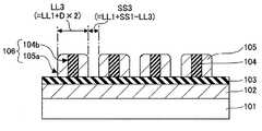
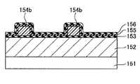
이어서, 단계(S16)의 공정을 포함하는 에칭 공정을 행한다. 단계(S16)는 SiO2막(105)이 레지스트 패턴(104b)의 측벽부(105a)로서만 남도록 에칭하는 에칭 공정이다. 또한, 도 2f는 단계(S16)의 공정이 행해진 후의 미세 패턴의 구조를 도시한 단면도이다.Next, the etching process including the process of step S16 is performed. Step S16 is an etching process for etching so that the SiO2 film 105 remains only as the
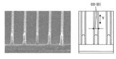
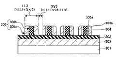
도 2f에 도시한 바와 같이, SiO2막(105)을 에칭하여 SiO2막(105)이 레지스트 패턴(104b)의 측면을 피복하는 측벽부(105a)로만 남은 상태로 한다. SiO2막(105)의 에칭은 특별히 한정되지 않고, 예를 들면 CF4, C4F8, CHF3, CH3F, CH2F2 등의 CF 계 가스와 Ar 가스 등의 혼합 가스, 또는 이 혼합 가스에 필요에 따라 산소를 첨가한 가스 등을 이용하여 행할 수 있다. SiO2막(105)으로 이루어지는 레지스트 패턴(104b)의 측벽부(105a)만이 남도록 에칭하기 때문에, 레지스트 패턴(104b) 및 측벽부(105a)로 이루어지는 제 3 패턴(106)이 형성된다. 제 3 패턴(106)의 라인폭을 LL3, 스페이스폭을 SS3으로 하면, 레지스트 패턴(104b)의 라인폭(LL1)이 30 nm, 측벽부(105a)의 두께(D)가 30 nm인 경우, LL3 = LL1 + D × 2, SS3 = LL1 + SS1 - LL3이므로 LL3을 90 nm, SS3을 30 nm로 할 수 있다.As shown in Fig. 2F, the SiO2 film 105 is etched so that the SiO2 film 105 remains only as the
또한, 단계(S16)의 에칭 공정에서 행하는 에칭을, 에칭에 의해 SiO2막(105)의 표면을 두께 방향으로 후퇴시킨다는 점에서 에치백(etch back)이라고도 한다.The etching performed in the etching step of step S16 is also referred to as etch back in that the surface of the SiO2 film 105 is retracted in the thickness direction by etching.
또한, 에칭 공정을 행함으로써, 산화막은 형상이 가공된 레지스트 패턴의 라인부의 측면에 측벽으로서 잔존하도록 에칭된다. 따라서, 에칭 공정은 산화막이 형상이 가공된 레지스트 패턴의 라인부의 측면에 측벽으로서 잔존하도록 산화막을 에 칭하는 공정이다.Further, by performing the etching step, the oxide film is etched so that the shape remains as sidewalls on the side surfaces of the line portions of the processed resist pattern. Therefore, the etching step is a step of etching the oxide film so that the oxide film remains as a side wall on the side of the line portion of the processed resist pattern.
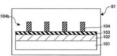
단계(S17)는 레지스트 패턴(104b)을 제거하여 측벽부(105a)를 형성하는 공정과, 또한 형성된 측벽부(105a)를 마스크로 하여 유기막(103)을 에칭하는 공정이다. 또한, 도 2g는 레지스트 패턴(104b)을 제거하는 공정과 유기막(103)을 에칭하는 공정이 행해진 후의 미세 패턴의 구조를 도시한 단면도이다.Step S17 is a step of removing the resist
산소, 질소, 수소, 암모니아 등의 플라즈마를 이용한 에칭을 행하고, 포토레지스트막(104)으로 이루어지는 레지스트 패턴(104b)을 제거함으로써, 측벽부(105a)만이 남는다. 또한, 남은 측벽부(105a)를 마스크로 하여 유기막(103)을 에칭함으로써, 도 2g에 도시한 바와 같이, 측벽부(105a) 및 유기막(103)으로 이루어지고, 라인폭이 D, 스페이스폭이 LL1 및 SS3이 교호적으로 나타나는 패턴인 제 2 패턴(107)이 형성된다. 그 결과, 도 2g에 도시한 바와 같이, 포토레지스트막(104)으로 이루어지는 레지스트 패턴(104b)이 제거되어 측벽부(105a)만이 남고, 라인폭이 D, 스페이스폭이 LL1 및 SS3이 교호적으로 나타나는 패턴인 제 2 패턴(107)이 형성된다. 본 실시예에서는, 레지스트 패턴(104b)의 라인폭(LL1)과 제 3 패턴(106)의 스페이스폭(SS3)을 동일하게 함으로써, 스페이스폭은 LL1 및 SS3과 동일한 SS2가 된다. 또한, D와 동일한 라인폭을 재차 LL2로 한다. 상술한 바와 같이, LL1을 30 nm, SS3을 30 nm, SiO2막(105)의 두께(측벽부(105a)의 폭(D))를 30 nm로 함으로써, 라인폭(LL2)이 30 nm, 스페이스폭(SS2)이 30 nm인 제 2 패턴(107)을 형성할 수 있다.By etching using plasma such as oxygen, nitrogen, hydrogen, ammonia, and the like, the resist
또한, 제 2 패턴(107)은 측벽부(105a) 및 유기막(반사 방지막)(103)으로 이 루어지고, 본 발명에서의 마스크 패턴에 상당한다.The
그 후, 제 2 패턴(107)을 마스크로 하여 박막(102)을 에칭한다. 즉, 단계(S18)를 행한다. 단계(S18)에서는 제 2 패턴(마스크 패턴)(107)을 이용하여 박막(피에칭막)(102)을 가공하여, 도 2h에 도시한 바와 같이, 박막(피에칭막)(102)으로 이루어지는 패턴(102a)을 형성한다. 패턴(102a)의 상부에는 유기막(반사 방지막)(103)이 남아 있어도 좋다. 예를 들면 비결정 실리콘 또는 폴리 실리콘으로 이루어지는 박막(102)의 에칭은, Cl2, Cl2 + HBr, Cl2 + O2, CF4 + O2, SF6, Cl2 + N2, Cl2 + HCl, HBr + Cl2 + SF6 등의 가스 등의 플라즈마를 이용하여 행할 수 있다. 즉, CF계 가스, CHF계 가스, CH계 가스, 또는 산소 가스 등을 포함하는 가스를 이용하여 행할 수 있다.Thereafter, the
또한, 유기막(반사 방지막)(103)을 형성하는 공정(단계(S11)의 일부)부터 측벽부(105a) 및 유기막(반사 방지막)(103)으로 이루어지는 마스크 패턴을 형성하는 공정(단계(S17))까지를, 본 발명에서의 마스크 패턴의 형성 방법이라고 정의한다. 또한, 그 마스크 패턴의 형성 방법을 포함하고 박막(피에칭막)(102)을 형성하는 공정(단계(S11)의 일부)부터 박막(피에칭막)(102)으로 이루어지는 패턴(102a)을 형성하는 공정(단계(S18))까지를, 본 발명에서의 미세 패턴의 형성 방법이라고 정의한다.Further, a step of forming a mask pattern including the
이어서, 도 3 및 도 4를 참조하여 본 실시예에 따른 미세 패턴의 형성 방법에 사용되는 성막 장치에 대하여 설명한다.Next, the film-forming apparatus used for the fine pattern formation method which concerns on this Example with reference to FIG. 3 and FIG. 4 is demonstrated.
도 3은 본 실시예에 따른 미세 패턴의 형성 방법에 사용되는 성막 장치의 구성을 모식적으로 도시한 종단면도이다. 도 4는 본 실시예에 따른 미세 패턴의 형성 방법에 사용되는 성막 장치의 구성을 모식적으로 도시한 횡단면도이다. 또한, 도 4에서는 가열 장치를 생략하고 있다.3 is a longitudinal sectional view schematically showing the configuration of a film forming apparatus used in the method for forming a fine pattern according to the present embodiment. 4 is a cross-sectional view schematically showing the configuration of a film forming apparatus used in the method for forming a fine pattern according to the present embodiment. In addition, the heating apparatus is abbreviate | omitted in FIG.
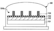
도 3에 도시한 바와 같이, 본 실시예에 따른 성막 장치(80)는 형상 가공 공정인 슬리밍 처리와 성막 공정인 성막 처리를 동일한 성막 장치 내에서 연속 처리하도록 한 것이다.As shown in FIG. 3, the film-forming
종래, 슬리밍 처리는 에칭 장치 또는 애싱 장치 등을 이용하여 행해지고, 성막 처리는 성막 장치를 이용하여 행해지고 있다. 이 때문에, 슬리밍 처리를 끝낸 반도체 기판(웨이퍼)은 애싱 장치로부터 일단 인출된 후 성막 장치로 반송되도록 되어 있다.Conventionally, a slimming process is performed using an etching apparatus, an ashing apparatus, etc., and a film-forming process is performed using a film-forming apparatus. For this reason, the semiconductor substrate (wafer) which finished the slimming process is once taken out from the ashing apparatus, and is conveyed to the film-forming apparatus.
이와 같이, 축소(shrink) 처리 후에 웨이퍼가 장치로부터 인출되기 때문에, 레지스트 패턴(104b)의 표면에 먼지 등이 부착될 가능성이 있다. 레지스트 패턴(104b)의 표면에 먼지 등이 부착되면, 레지스트 패턴(104b) 상에 형성되는 SiO2막(105)에서는 결함 밀도가 증가하고, 또한 그 막두께의 균일성이 쉽게 손상되게 된다.In this manner, since the wafer is taken out from the apparatus after the shrinking process, dust or the like may adhere to the surface of the resist
이에 대하여, 본 실시예에 따른 성막 장치(80)는 슬리밍 처리를 성막 장치를 이용하여 행하도록 하고, 또한 슬리밍 처리와 성막 처리를 동일한 성막 장치 내에서 연속 처리하도록 한다. 이에 의해, 레지스트 패턴(104b)의 표면을 청정하게 유 지한 채로 SiO2막(105)을 성막할 수 있고, 그 결함 밀도를 저감시키고, 또한 막두께의 균일성을 높이는 것이 가능해진다고 하는 이점도 얻을 수 있다.In contrast, the
또한, 상기 2 개의 처리를 동일 장치 내에서 연속적으로 행함으로써 반송 또는 대기 시간(Queing-time)을 저감시켜 생산 효율을 향상시키고 비용을 저감할 수 있다고 하는 효과도 있다.In addition, by carrying out the above two processes in the same apparatus continuously, there is an effect that the conveyance or the waiting time (Queing-time) can be reduced to improve the production efficiency and the cost can be reduced.
도 3 및 도 4에 도시한 바와 같이, 성막 장치(80)는 하단이 개구된 천장이 있는 원통체 형상의 처리 용기(1)를 가지고 있다. 이 처리 용기(1)의 전체는, 예를 들면 석영에 의해 형성되어 있고, 이 처리 용기(1) 내의 천장에는 석영제의 천장판(2)이 설치되어 봉지(封止)되고 있다. 또한, 이 처리 용기(1)의 하단 개구부에는, 예를 들면 스테인레스 스틸에 의해 원통체 형상으로 성형된 매니폴드(3)가 O 링 등의 씰 부재(4)를 개재하여 연결되어 있다.As shown in FIG. 3 and FIG. 4, the film-forming
상기 매니폴드(3)는 처리 용기(1)의 하단을 지지하고 있고, 이 매니폴드(3)의 하방으로부터 피처리체로서 다수 매, 예를 들면 50 ~ 100 매의 반도체 웨이퍼(W)를 다단으로 재치 가능한 석영제의 웨이퍼 보트(5)가 처리 용기(1) 내로 삽입 가능하도록 되어 있다. 이 웨이퍼 보트(5)는 3 개의 지지 기둥(6)을 가지고(도 4 참조), 지지 기둥(6)에 형성된 홈에 의해 다수 매의 웨이퍼(W)가 지지되도록 되어 있다.The manifold 3 supports the lower end of the
이 웨이퍼 보트(5)는 석영제의 보온통(7)을 개재하여 테이블(8) 상에 재치되어 있고, 이 테이블(8)은 매니폴드(3)의 하단 개구부를 개폐하는, 예를 들면 스테 인레스 스틸제의 덮개부(9)를 관통하는 회전축(10) 상에 지지된다.The
그리고, 이 회전축(10)의 관통부에는, 예를 들면 자성 유체 씰(11)이 설치되어 있어 회전축(10)을 기밀하게 밀폐하면서 회전 가능하게 지지되어 있다. 또한, 덮개부(9)의 주변부와 매니폴드(3)의 하단부의 사이에는, 예를 들면 O 링으로 이루어지는 씰 부재(12)가 개재되어 있어, 이에 의해 처리 용기(1) 내의 밀폐성을 유지하고 있다.And the magnetic fluid seal 11 is provided in the penetrating part of this rotating
상기의 회전축(10)은, 예를 들면 보트 엘리베이터 등의 승강 기구(도시하지 않음)에 지지된 암(13)의 선단에 장착되어 있고, 웨이퍼 보트(5) 및 덮개부(9) 등을 일체적으로 승강시켜 처리 용기(1) 내에 대하여 삽탈(揷脫)되도록 되어 있다. 또한, 상기 테이블(8)을 상기 덮개부(9)측에 고정하여 설치하고, 웨이퍼 보트(5)를 회전시키지 않고 웨이퍼(W)의 처리를 행하도록 해도 좋다.The
또한, 성막 장치(80)는 처리 용기(1) 내로 산소 함유 가스, 예를 들면 O2 가스를 공급하는 산소 함유 가스 공급 기구(14)와, 처리 용기(1) 내로 Si 소스 가스를 공급하는 Si 소스 가스 공급 기구(15)와, 처리 용기(1) 내로 퍼지 가스로서 불활성 가스, 예를 들면 N2 가스를 공급하는 퍼지 가스 공급 기구(16)를 가지고 있다.The
또한, 산소 함유 가스 공급 기구(14)는 본 발명에서의 산소 래디컬 공급 수단에 상당하고, Si 소스 가스 공급 기구(15)는 본 발명에서의 소스 가스 공급 수단에 상당한다.The oxygen-containing
산소 함유 가스 공급 기구(14)는, 산소 함유 가스 공급원(17)과, 산소 함유 가스 공급원(17)으로부터 산소 함유 가스를 유도하는 산소 함유 가스 배관(18)과, 이 산소 함유 가스 배관(18)에 접속되고 매니폴드(3)의 측벽을 내측으로 관통하여 상방향으로 굴곡되어 수직으로 연장되는 석영관으로 이루어지는 산소 함유 가스 분산 노즐(19)을 가지고 있다. 이 산소 함유 가스 분산 노즐(19)의 수직 부분에는 복수의 가스 토출홀(19a)이 소정의 간격을 두고 형성되어 있고, 각 가스 토출홀(19a)로부터 수평 방향으로 처리 용기(1)를 향하여 실질적으로 균일하게 산소 함유 가스, 예를 들면 O2 가스를 토출할 수 있도록 되어 있다.The oxygen-containing
또한, Si 소스 가스 공급 기구(15)는, Si 소스 가스 공급원(20)과, 이 Si 소스 가스 공급원(20)으로부터 Si 소스 가스를 유도하는 Si 소스 가스 배관(21)과, 이 Si 소스 가스 배관(21)에 접속되고 매니폴드(3)의 측벽을 내측으로 관통하여 상방향으로 굴곡되어 수직으로 연장되는 석영관으로 이루어지는 Si 소스 가스 분산 노즐(22)을 가지고 있다. 여기서는 Si 소스 가스 분산 노즐(22)은 2 개 설치되어 있고(도 4 참조), 각 Si 소스 가스 분산 노즐(22)에는 그 길이 방향을 따라 복수의 가스 토출홀(22a)이 소정의 간격을 두고 형성되어 있고, 각 가스 토출홀(22a)로부터 수평 방향으로 처리 용기(1) 내로 실질적으로 균일하게 유기 실리콘을 포함하는 Si 소스 가스를 토출할 수 있도록 되어 있다. 또한, Si 소스 가스 분산 노즐(22)은 1 개뿐이어도 좋다.The Si source
또한, 퍼지 가스 공급 기구(16)는, 퍼지 가스 공급원(23)과, 퍼지 가스 공급원(23)으로부터 퍼지 가스를 유도하는 퍼지 가스 배관(24)과, 이 퍼지 가스 배 관(24)에 접속되고 매니폴드(3)의 측벽을 관통하여 설치된 퍼지 가스 노즐(25)을 가지고 있다. 퍼지 가스로서는 불활성 가스, 예를 들면 N2 가스를 적합하게 이용할 수 있다.In addition, the purge
산소 함유 가스 배관(18), Si 소스 가스 배관(21), 퍼지 가스 배관(24)에는 각각 개폐 밸브(18a, 21a, 24a) 및 매스 플로우 콘트롤러와 같은 유량 제어기(18b, 21b, 24b)가 설치되어 있어, 산소 함유 가스, Si 소스 가스 및 퍼지 가스를 각각 유량 제어하면서 공급할 수 있도록 되어 있다.In the oxygen-containing
상기 처리 용기(1)의 측벽의 일부에는 산소 함유 가스의 플라즈마를 형성하는 플라즈마 생성 기구(30)가 형성되어 있다. 이 플라즈마 생성 기구(30)는, 상기 처리 용기(1)의 측벽을 상하 방향을 따라 소정의 폭으로 제거함으로써 상하로 길고 가늘게 형성된 개구(31)를 그 외측으로부터 덮도록 하여 처리 용기(1)의 외벽에 기밀하게 용접된 플라즈마 구획벽(32)을 가지고 있다. 플라즈마 구획벽(32)은 단면 오목부 형상을 이루며 상하로 길고 가늘게 형성되고, 예를 들면 석영으로 형성되어 있다. 또한, 플라즈마 생성 기구(30)는 이 플라즈마 구획벽(32)의 양측벽의 외면에 상하 방향을 따라 서로 대향하도록 하여 배치된 길고 가는 한 쌍의 플라즈마 전극(33)과, 이 플라즈마 전극(33)에 급전 라인(34)을 개재하여 접속되고 고주파 파워를 공급하는 고주파 전원(35)을 가지고 있다. 그리고, 상기 플라즈마 전극(33)에 고주파 전원(35)으로부터, 예를 들면 13.56 MHz의 고주파 전압을 인가함으로써 산소 함유 가스의 플라즈마가 발생할 수 있다. 또한 이 고주파 전압의 주파수는 13.56 MHz로 한정되지 않고 다른 주파수, 예를 들면 400 kHz 등을 이용해도 좋다.A part of the side wall of the
상기와 같은 플라즈마 구획벽(32)을 형성함으로써 처리 용기(1)의 측벽의 일부가 오목부 형상으로 외측으로 돌출된 상태가 되고, 플라즈마 구획벽(32)의 내부 공간이 처리 용기(1)의 내부 공간에 일체적으로 연통된 상태가 된다. 또한, 개구(31)는 웨이퍼 보트(5)에 유지되어 있는 모든 웨이퍼(W)를 높이 방향에서 커버할 수 있도록 상하 방향으로 충분히 길게 형성되어 있다.By forming the
상기 산소 함유 가스 분산 노즐(19)은 처리 용기(1) 내를 상방향으로 연장하고 있는 도중에 처리 용기(1)의 반경 방향 외방으로 굴곡되고, 상기 플라즈마 구획벽(32) 내의 가장 내측 부분(처리 용기(1)의 중심으로부터 가장 떨어진 부분)을 따라 상방을 항하여 기립되어 있다. 이 때문에, 고주파 전원(35)이 온(on)되어 양전극(33) 간에 고주파 전계가 형성되었을 때에, 산소 함유 가스 분산 노즐(19)의 가스 토출홀(19a)로부터 토출된 산소 가스가 플라즈마화되어 처리 용기(1)의 중심을 향하여 확산되면서 흐른다.The oxygen-containing
상기 플라즈마 구획벽(32)의 외측에는 이를 덮도록 하여, 예를 들면 석영으로 이루어지는 절연 보호 커버(36)가 장착되어 있다. 또한, 이 절연 보호 커버(36)의 내측 부분에는 도시하지 않은 냉매 통로가 설치되어 있고, 예를 들면 냉각된 질소 가스를 유입시킴으로써 상기 플라즈마 전극(33)을 냉각할 수 있도록 되어 있다.An outer
상기 2 개의 Si 소스 가스 분산 노즐(22)은 처리 용기(1)의 내측벽 상기 개구(31)를 사이에 둔 위치에 기립하여 설치되어 있고, 이 Si 소스 가스 분산 노즐(22)에 형성된 복수의 가스 토출홀(22a)로부터 처리 용기(1)의 중심 방향을 향하 여 Si 소스 가스로서 1 분자 내에 1 개 또는 2 개의 아미노기를 가지는 아미노실란 가스를 토출할 수 있도록 되어 있다.The two Si source
한편, 처리 용기(1)의 개구(31)의 반대측 부분에는 처리 용기(1) 내를 진공 배기하기 위한 배기구(37)가 설치되어 있다. 이 배기구(37)는 처리 용기(1)의 측벽을 상하 방향으로 제거함으로써 길고 가늘게 형성되어 있다. 처리 용기(1)의 이 배기구(37)에 대응하는 부분에는 배기구(37)를 덮도록 단면 오목부 형상으로 성형된 배기구 커버 부재(38)가 용접에 의해 장착되어 있다. 이 배기구 커버 부재(38)는, 처리 용기(1)의 측벽을 따라 상방으로 연장되어 있고, 처리 용기(1)의 상방에 가스 출구(39)를 규정하고 있다. 그리고, 이 가스 출구(39)로부터 도시하지 않은 진공 펌프 등을 포함하는 진공 배기 기구에 의해 진공 배기된다. 그리고, 이 처리 용기(1)의 외주를 둘러싸도록 하여 이 처리 용기(1) 및 그 내부의 웨이퍼(W)를 가열하는 케이스 형상의 가열 장치(40)가 설치되어 있다.On the other hand, the
성막 장치(80)의 각 구성부의 제어, 예를 들면 밸브(18a, 21a, 24a)의 개폐에 의한 각 가스의 공급·정지, 매스 플로우 콘트롤러(18b, 21b, 24b)에 의한 가스 유량의 제어, 및 고주파 전원(35)의 온·오프 제어, 가열 장치(40)의 제어 등은, 예를 들면 마이크로 프로세서(컴퓨터)로 이루어지는 콘트롤러(50)에 의해 행해진다. 콘트롤러(50)에는 공정 관리자가 성막 장치(80)를 관리하기 위하여 커멘드의 입력 조작 등을 행하는 키보드, 또는 성막 장치(80)의 가동 상황을 가시화하여 표시하는 디스플레이 등으로 이루어지는 유저 인터페이스(51)가 접속되어 있다.Control of each component of the
또한, 콘트롤러(50)에는 성막 장치(80)에서 실행되는 각종 처리를 콘트롤 러(50)의 제어로 실현시키기 위한 제어 프로그램, 또는 처리 조건에 따라 성막 장치(80)의 각 구성부에 처리를 실행시키기 위한 프로그램, 즉 레시피가 저장된 기억부(52)가 접속되어 있다. 레시피는 기억부(52) 내의 기억 매체에 기억되어 있다. 기억 매체는 하드 디스크 또는 반도체 메모리여도 좋고, CD-ROM, DVD, 플래쉬 메모리 등의 휴대 가능한 것이어도 좋다. 또한, 다른 장치로부터, 예를 들면 전용 회선을 거쳐 레시피를 적절히 전송하도록 해도 좋다.In addition, the
그리고, 필요에 따라 유저 인터페이스(51)로부터의 지시 등으로 임의의 레시피를 기억부(52)로부터 호출하여 콘트롤러(50)에 실행시킴으로써, 콘트롤러(50)의 제어 하에 성막 장치(80)에서의 원하는 처리가 행해진다.Then, if necessary, an arbitrary recipe is called from the
이어서, 도 5 및 도 6을 참조하여 본 실시예에 따른 미세 패턴의 형성 방법의 형상 가공 공정 및 성막 공정에서의 처리에 대하여 설명한다.Next, with reference to FIGS. 5 and 6, the processing in the shape processing step and the film formation step of the method for forming a fine pattern according to the present embodiment will be described.
도 5는 본 실시예에 따른 미세 패턴의 형성 방법을 설명하기 위한 도이며, 형상 가공 공정 및 성막 공정에서의 가스 공급 타이밍을 도시한 타이밍 차트이다. 도 6은 본 실시예에 따른 미세 패턴의 형성 방법을 설명하기 위한 도이며, Si 소스 가스에 BTBAS를 이용했을 때의 반도체 기판 상에서의 반응을 모식적으로 도시한 도이다.FIG. 5 is a diagram for explaining a method for forming a fine pattern according to the present embodiment, and is a timing chart showing the gas supply timing in the shape processing step and the film formation step. FIG. 6 is a diagram for explaining a method for forming a fine pattern according to the present embodiment, which schematically illustrates a reaction on a semiconductor substrate when BTBAS is used as the Si source gas.
예를 들면, 50 ~ 100 매의 반도체 웨이퍼(W)가 탑재된 상태의 웨이퍼 보트(5)를 미리 소정의 온도로 제어된 처리 용기(1) 내로 그 하방으로부터 상승시킴으로써 로드하고, 덮개부(9)로 매니폴드(3)의 하단 개구부를 폐쇄함으로써 처리 용기(1) 내를 밀폐 공간으로 한다. 웨이퍼(W)로서는 직경 300 mm인 것이 예시된다. 처리 용기(1) 내를 소정의 프로세스 압력으로 유지하고, 또한 가열 장치(40)로의 공급 전력을 제어하여 웨이퍼 온도를 상승시켜 프로세스 온도로 유지하고, 웨이퍼 보트(5)를 회전시킨다.For example, the
단, 본 실시예에서는 성막 공정을 개시하기 전에 레지스트 패턴의 형상을 가공하는 형상 가공 공정을 행한다.In the present embodiment, however, the shape processing step of processing the shape of the resist pattern is performed before starting the film formation step.
도 5에 도시한 바와 같이, 형상 가공 공정에서는, 산소 함유 가스를 여기시켜 형성된 산소 래디컬을 처리 용기(1)로 공급하여 레지스트 패턴의 형상을 가공하는(슬리밍 처리하는) 공정(S1)을 실시한다.As shown in FIG. 5, in the shape processing step, oxygen radicals formed by exciting the oxygen-containing gas are supplied to the
공정(S1)의 산소 래디컬을 공급하는 공정에서는, 산소 함유 가스 공급 기구(14)의 산소 함유 가스 공급원(17)으로부터 산소 함유 가스로서, 예를 들면 O2 가스를 산소 함유 가스 배관(18) 및 산소 함유 가스 분산 노즐(19)을 거쳐 가스 토출홀(19a)로부터 토출하고, 이 때 플라즈마 생성 기구(30)의 고주파 전원(35)을 온(on)으로 하여 고주파 전계를 형성하고, 이 고주파 전계에 의해 산소 함유 가스, 예를 들면 O2 가스를 플라즈마화한다. 그리고, 이와 같이 플라즈마화된 산소 함유 가스를 처리 용기(1) 내로 공급한다. 이에 따라, 레지스트 패턴을 형성하는 포토레지스트가 애싱 처리됨으로써 레지스트 패턴의 폭 및 높이가 감소하는, 즉 슬리밍 처리가 행해진다. 이 처리 시간(T1)은 1 ~ 600 sec의 범위가 예시된다. 또한, 산소 함유 가스의 유량은 반도체 웨이퍼(W)의 탑재 매수에 따라서도 상이하지만, 100 ~ 20000 mL/min(sccm)가 예시된다. 또한, 고주파 전원(35)의 주파수는 13.56 MHz가 예시되고, 파워로서는 5 ~ 1000 W가 채용된다. 또한, 이 때의 처리 용기(1) 내의 압력은 13.3 ~ 665 Pa가 예시된다.In the step of supplying the oxygen radical in the step S1, for example, O2 gas is used as the oxygen-containing gas from the oxygen-containing
이 경우에, 산소 함유 가스로서는, O2 가스 외에 NO 가스, N2O 가스, H2O 가스, O3 가스를 들 수 있고, 이들을 고주파 전계에 의해 플라즈마화하여 이용한다. 산소 래디컬이면 산소 함유 가스의 플라즈마에 한정되지 않지만, 산소 함유 가스의 플라즈마를 형성하는 것이 바람직하고, 그 중에서도 O2 플라즈마가 바람직하다. 산화제로서 산소 래디컬, 특히 산소 함유 가스의 플라즈마를 이용함으로써 슬리밍 처리를 행할 때의 기판 온도가 300℃ 이하, 더욱 바람직하게는 100℃ 이하, 이상적으로는 실온에서도 슬리밍 처리가 가능하다.In this case, as the oxygen-containing gas, there may be mentioned O2 gas in addition to the NO gas, N2 O gas, H2 O gas, O3 gas, and use them to plasma by the high frequency electric field. When oxygen radicals, but not limited to a plasma of an oxygen-containing gas, it is preferable to form a plasma in the oxygen-containing gas and, particularly O2 plasma is preferred. By using oxygen radicals, in particular, plasma of oxygen-containing gas, as an oxidizing agent, the substrate temperature at the time of slimming treatment is 300 ° C or lower, more preferably 100 ° C or lower, and ideally, slimming can be performed even at room temperature.
다음에, 형상 가공 공정에 이어서 처리 용기(1) 내에서 성막 공정을 행한다.Next, the film formation process is performed in the
우선, 형상 가공 공정 후 성막 공정을 개시하기 전에 공정(S2)이 행해진다. 공정(S2)은 공정(S1) 후에 처리 용기(1) 내에 잔류하는 가스를 제거하여 다음의 공정에서 원하는 반응을 발생시키는 공정이며, 처리 용기(1) 내를 진공 배기하면서 퍼지 가스 공급 기구(16)의 퍼지 가스 공급원(23)으로부터 퍼지 가스 배관(24) 및 퍼지 가스 노즐(25)을 거쳐 퍼지 가스로서 불활성 가스, 예를 들면 N2 가스를 공급함으로써 행해진다. 이 공정(S2)의 시간(T2)으로서는 1 ~ 60 sec가 예시된다. 또한, 퍼지 가스 유량으로서는 0.1 ~ 5000 mL/min(sccm)가 예시된다. 또한, 이 공정(S2)은 처리 용기(1) 내에 잔류하고 있는 가스를 제거할 수 있으면, 퍼지 가스를 공급하지 않고 모든 가스의 공급을 정지한 상태에서 진공 배기를 계속하여 행하도 록 해도 좋다. 단, 퍼지 가스를 공급함으로써 단시간에 처리 용기(1) 내의 잔류 가스를 제거할 수 있다. 또한, 이 때의 처리 용기(1) 내의 압력은 0.133 ~ 665 Pa가 예시된다. 또한, 기판 온도는 실온(25℃) ~ 700℃, 바람직하게는 실온(25℃) ~ 500℃, 더욱 바람직하게는 실온(25℃) ~ 300℃이 예시된다.First, a process (S2) is performed before starting a film-forming process after a shape processing process. The step S2 is a step of removing the gas remaining in the
이어서, 처리 용기(1) 내를 소정의 프로세스 압력으로 유지하고, 또한 가열 장치(40)로의 공급 전력을 제어하여 웨이퍼 온도를 상승시켜 프로세스 온도로 유지하고, 웨이퍼 보트(5)를 회전시킨 상태에서 성막 처리를 개시한다.Subsequently, the inside of the
도 5에 도시한 바와 같이, 본 실시예에서는, 유기 실리콘을 포함하는 Si 소스 가스를 처리 용기(1) 내로 유입시켜 Si 소스를 흡착시키는 공정(S3)과, 산소 함유 가스를 여기시켜 형성된 산소 래디컬을 처리 용기(1)로 공급하여 Si 소스 가스를 산화시키는 공정(S4)을 교호적으로 반복한다. 또한, 본 실시예에서는, 공정(S3)과 공정(S4)의 사이에 처리 용기(1) 내로부터 처리 용기(1) 내에 잔류하는 가스를 제거하는 공정(S5)을 행한다.As shown in Fig. 5, in this embodiment, a step (S3) in which a Si source gas containing organic silicon is introduced into the
구체적으로, 본 실시예에서는, 공정(S3)에서 Si 소스 가스 공급 기구(15)의 Si 소스 가스 공급원(20)으로부터 Si 소스 가스로서 1 분자 내에 2 개의 아미노기를 가지는 아미노실란 가스, 예를 들면 BTBAS를 Si 소스 가스 배관(21) 및 Si 소스 가스 분산 노즐(22)을 거쳐 가스 토출홀(22a)로부터 처리 용기(1) 내로 T3 시간 공급한다. 이에 따라 반도체 웨이퍼에 Si 소스 가스를 흡착시킨다. 이 때의 시간(T3)은 1 ~ 600 sec가 예시된다. 또한, Si 소스 가스의 유량은 10 ~ 500 mL/min(sccm)가 예시된다. 또한, 이 때의 처리 용기(1) 내의 압력은 13.3 ~ 665 Pa가 예시된다.Specifically, in this embodiment, aminosilane gas having two amino groups in one molecule as Si source gas from Si source
공정(S4)의 산소 래디컬을 공급하는 공정에서는, 공정(S1)과 마찬가지로 산소 함유 가스 공급 기구(14)의 산소 함유 가스 공급원(17)으로부터 산소 함유 가스로서, 예를 들면 O2 가스를 산소 함유 가스 배관(18) 및 산소 함유 가스 분산 노즐(19)을 거쳐 가스 토출홀(19a)로부터 토출하고, 이 때 플라즈마 생성 기구(30)의 고주파 전원(35)을 온(on)으로 하여 고주파 전계를 형성하고, 이 고주파 전계에 의해 산소 함유 가스, 예를 들면 O2 가스를 플라즈마화한다. 그리고, 이와 같이 플라즈마화 된 산소 함유 가스를 처리 용기(1) 내로 공급한다. 이에 따라 반도체 웨이퍼(W)에 흡착된 Si 소스가 산화된 SiO2가 형성된다. 이 처리 시간(T4)은 1 ~ 600 sec의 범위가 예시된다. 또한, 산소 함유 가스의 유량은 반도체 웨이퍼(W)의 탑재 매수에 따라서도 상이하지만, 100 ~ 20000 mL/min(sccm)가 예시된다. 또한, 고주파 전원(35)의 주파수는 13.56 MHz가 예시되고, 파워로서는 5 ~ 1000 W가 채용된다. 또한, 이 때의 처리 용기(1) 내의 압력은 13.3 ~ 665 Pa가 예시된다.In the step of supplying the oxygen radical in the step S4, for example, O2 gas is contained as an oxygen-containing gas from the oxygen-containing
이 경우에도, 산소 함유 가스로서는, 공정(S1)과 마찬가지로, O2 가스 외에 NO 가스, N2O 가스, H2O 가스, O3 가스를 들 수 있고, 이들을 고주파 전계에 의해 플라즈마화하여 산화제로서 이용한다. 산화제로서는 산소 래디컬이면 산소 함유 가스의 플라즈마에 한정되지 않지만, 산소 함유 가스의 플라즈마를 형성하는 것이 바람직하고, 그 중에서도 O2 플라즈마가 바람직하다. 산화제로서 산소 래디컬, 특히 산소 함유 가스의 플라즈마를 이용함으로써, SiO2 막의 성막이 300℃ 이하, 더욱 바 람직하게는 100℃ 이하, 이상적으로는 실온에서도 성막이 가능하다.Also in this case, as with the Examples of the oxygen-containing gas, the process (S1), O2 gas in addition to NO gas, N2 O gas, H2 O gas, O3 may be mentioned the gas them to plasma by the high frequency electric field oxidant It is used as. Examples of the oxidizing agent is oxygen radicals, but not limited to a plasma of an oxygen-containing gas, it is preferable to form a plasma in the oxygen-containing gas and, particularly O2 plasma is preferred. By using oxygen radicals, in particular, plasma of oxygen-containing gas, as the oxidizing agent, film formation of SiO2 film is 300 ° C. or lower, more preferably 100 ° C. or lower, and ideally at room temperature.
또한, 공정(S3)과 공정(S4)의 사이에 행해지는 공정(S5)은, 공정(S3) 후 또는 공정(S4) 후에 처리 용기(1) 내에 잔류하는 가스를 제거하여 다음의 공정에서 원하는 반응을 발생시키는 공정이며, 처리 용기(1) 내를 진공 배기하면서 퍼지 가스 공급 기구(16)의 퍼지 가스 공급원(23)으로부터 퍼지 가스 배관(24) 및 퍼지 가스 노즐(25)을 거쳐 퍼지 가스로서 불활성 가스, 예를 들면 N2 가스를 공급함으로써 행해진다. 이 공정(S5) 시간(T5)으로서는 1 ~ 60 sec가 예시된다. 또한, 퍼지 가스 유량으로서는 0.1 ~ 5000 mL/min(sccm)가 예시된다. 또한, 이 공정(S5)은 처리 용기(1) 내에 잔류하고 있는 가스를 제거할 수 있으면, 퍼지 가스를 공급하지 않고 모든 가스의 공급을 정지한 상태에서 진공 배기를 계속하여 행하도록 해도 좋다. 단, 퍼지 가스를 공급함으로써 단시간에 처리 용기(1) 내의 잔류 가스를 제거할 수 있다. 또한, 이 때의 처리 용기(1) 내의 압력은 0.133 ~ 665 Pa가 예시된다.In addition, the process S5 performed between the process S3 and the process S4 removes the gas remaining in the
이와 같이 하여, 공정(S3)과 공정(S4) 간에 처리 용기(1) 내로부터 가스를 제거하는 공정(S5)을 사이에 두고 교호적으로 간헐적으로 Si 소스 가스와 산소 래디컬로서의 산소 함유 플라즈마를 반복 공급함으로써, SiO2막의 얇은 막을 한층씩 반복 적층하여 소정의 두께로 할 수 있다.In this manner, the Si source gas and the oxygen-containing plasma as oxygen radicals are alternately intermittently interposed between the step S3 and the step S4 with the step S5 of removing the gas from the inside of the
이 때의 반응예를 도 6에 도시한다. 도 6에는 반응예가 모식적으로 도시된다. 본 반응예에서는, 일례로서 Si 소스 가스에 BTBAS를 이용했을 때를 예시한다.The reaction example at this time is shown in FIG. 6, the reaction example is shown typically. In this reaction example, the case where BTBAS is used for Si source gas is illustrated as an example.
도 6(a)에 도시한 바와 같이, 이미 퇴적된 SiO2막의 표면에는 OH 기가 존재 하고 있고, 거기에 Si 소스로서, 예를 들면 BTBAS가 공급된다. 그리고, Si 소스가 흡착되는 공정(공정(S3))에서는, 도 6(b)에 도시한 바와 같이, BTBAS의 Si가 표면의 OH 기의 O와 반응하여 트리메틸아미노산을 이탈시킨다. 이 때, 아미노산을 2 개 가지는 아미노실란인 BTBAS는 OH와의 반응성이 높고, 또한, 구조적으로 이러한 Si의 반응의 장해가 되기 어렵기 때문에, Si의 흡착 반응이 신속하게 진행된다. 이 때 이탈한 트리메틸아미노기는 공정(S3)에 의해 처리 용기(1)로부터 제거된다. 그리고, 다음의 산화 공정(공정(S4))에서는, 도 6(c)에 도시한 바와 같이, 트리메틸아미노기가 이탈한 후의 Si 화합물이 O2 가스 플라즈마와 같은 산소 래디컬에 의해 산화되어 SiO2가 된다(단, 표면에는 H가 흡착되어 OH 기가 형성되어 있다). 이와 같이 O2 가스 플라즈마와 같은 산소 래디컬을 이용한 산화 반응은 순수한 화학적 반응과 달리 높은 온도가 불필요하므로 저온에서의 반응이 가능하다.As shown in Fig. 6 (a), OH groups exist on the surface of the SiO2 film that has already been deposited, and BTBAS is supplied thereto as a Si source. In the step (step S3) in which the Si source is adsorbed, as shown in Fig. 6 (b), Si of BTBAS reacts with O of the OH group on the surface to release trimethylamino acid. At this time, BTBAS, which is an aminosilane having two amino acids, has high reactivity with OH and is unlikely to hinder such reaction of Si structurally, so that the adsorption reaction of Si proceeds rapidly. At this time, the separated trimethylamino group is removed from the
BTBAS는 Si 소스 가스로서 이용하는 1 분자 내에 2 개의 아미노기를 가지는 아미노실란 가스이다. 이러한 아미노실란 가스로서는, 상술한 바와 같이 상기 BTBAS 외에 BDBAS(비스디에틸아미노실란), BDMAS(비스디메틸아미노실란)을 들 수 있다.BTBAS is aminosilane gas which has two amino groups in 1 molecule used as Si source gas. As such aminosilane gas, BDBAS (bisdiethylaminosilane) and BDMAS (bisdimethylaminosilane) are mentioned in addition to said BTBAS as mentioned above.
또한, Si 소스 가스에는 1 분자 내 3 개 이상의 아미노기를 가지는 아미노실란 가스를 이용하는 것도 가능하며, 1 분자 내에 1 개의 아미노기를 가지는 아미노실란 가스를 이용하는 것도 가능하다.As the Si source gas, an aminosilane gas having three or more amino groups in one molecule can be used, and an aminosilane gas having one amino group in one molecule can also be used.
본 실시예에서의 성막 공정을 행하면, Si 소스로서 유기 실리콘을 포함하는 소스 가스를 이용하고, 산화 처리에서 반응이 온도를 상승시키지 않고 진행하는 O2 가스 플라즈마와 같은 산소 래디컬을 이용하여 이들을 교호적으로 공급하므로, 양호한 막질의 SiO2막을 100℃ 이하, 나아가서는 실온이라고 하는, 종래에는 생각할 수 없었던 저온에서 또한 높은 성막 레이트로 성막할 수 있다.In the film forming step of the present embodiment, the source gas containing organic silicon is used as the Si source, and these are alternately made by using an oxygen radical such as an O2 gas plasma in which the reaction proceeds without raising the temperature in the oxidation treatment. As a result, the SiO2 film having a good film quality can be formed at a low filming rate and a high film forming rate, which is not conceivable in the past, such as 100 ° C. or lower, or room temperature.
이와 같이, 본 실시예에서는, 원리적으로 100℃ 이하라고 하는 극저온에서 성막할 수 있지만, 그보다 높은 온도여도 성막이 가능하다. 단, 성막 온도가 상승함에 따라 막두께 불균일이 커지는 것과 레지스트 패턴(104b)에 미치는 열적인 영향을 고려하면, 성막 온도는 100℃ 이하인 것이 가장 바람직하다.As described above, in the present embodiment, the film can be formed at a cryogenic temperature of 100 ° C. or lower in principle, but film formation is possible even at a higher temperature. However, considering the increase in film thickness unevenness as the film forming temperature increases and the thermal effect on the resist
이어서, 도 7a 내지 도 7c, 도 8a 내지 도 8d를 참조하여 본 실시예에 따른 미세 패턴의 형성 방법의 형상 가공 공정을 행함으로써, 공정을 삭감할 수 있는 작용 효과에 대하여 설명한다.Next, with reference to FIGS. 7A-7C and 8A-8D, the effect which can reduce a process by performing the shape processing process of the formation method of a fine pattern which concerns on a present Example is demonstrated.
도 7a 내지 도 7c는 본 실시예에 따른 미세 패턴의 형성 방법을 설명하기 위한 도이며, 형상 가공 공정 및 성막 공정에서의 미세 패턴의 구조를 모식적으로 도시한 단면도이다. 도 8a 내지 도 8d는 본 실시예에 따른 미세 패턴의 형성 방법을 설명하기 위한 도이며, 형상 가공 공정을 종래의 방법으로 행하는 경우의 형상 가공 공정 및 성막 공정에서의 미세 패턴의 구조를 모식적으로 도시한 단면도이다. 도 7a, 도 7b, 도 7c는 도 2c, 도 2d, 도 2e에 대응되고, 도 8a, 도 8b, 도 8d는 도 2c, 도 2d, 도 2e에 대응된다.7A to 7C are diagrams for explaining a method for forming a fine pattern according to the present embodiment, and are sectional views schematically showing the structure of the fine pattern in the shape processing step and the film formation step. 8A to 8D are diagrams for explaining a method for forming a fine pattern according to the present embodiment, and schematically show the structure of the fine pattern in the shape processing step and the film formation step when the shape processing step is performed by a conventional method. It is sectional drawing. 7A, 7B, and 7C correspond to FIGS. 2C, 2D, and 2E, and FIGS. 8A, 8B, and 8D correspond to FIGS. 2C, 2D, and 2E.
본 실시예에 따른 미세 패턴의 형성 방법에서는, 도 2c에 도시한 패턴 가공 공정이 행해진 후, 레지스트(104)가 레지스트 패턴(104a)으로 가공된 반도체 웨이퍼(W)는, 도 7a에 도시한 바와 같이 성막 장치(80) 내로 도입된다. 이어서, 도 7b에 도시한 바와 같이, 성막 장치(80) 내에서 산소 함유 가스 플라즈마 또는 오존 가스를 이용하여 레지스트 패턴(104a)의 형상을 레지스트 패턴(104b)으로 가공하는 형상 가공 공정(성막 장치 내 슬리밍 처리 공정)이 행해진다. 이어서, 도 7c에 도시한 바와 같이, 성막 장치(80) 내에서 계속해서 형상 가공 공정에 의해 형상이 가공된 레지스트 패턴(104b) 및 유기막(103) 상에 아미노실란계 전구체와 산소 함유 가스 플라즈마 또는 오존 가스를 이용하여 SiO2막(105)을 성막하는 성막 공정이 행해진다. 그 후, 에칭 장치로 도입되고 도 2f에 도시한 에칭 공정이 행해진다.In the method for forming a fine pattern according to the present embodiment, after the pattern processing step shown in FIG. 2C is performed, the semiconductor wafer W whose resist 104 is processed into the resist
여기서, 종래는 도 8a 내지 도 8d에 도시한 바와 같이, 도 2c에 도시한 패턴 가공 공정이 행해진 후 레지스트(104)가 레지스트 패턴(104a)으로 가공된 반도체 웨이퍼(W)는, 도 8a에 도시한 바와 같이 레지스트 도포 장치(또는 애싱 장치)(81)로 도입된다. 이어서, 도 8b에 도시한 바와 같이, 레지스트 도포 장치(또는 애싱 장치)(81) 내에서 포토리소그래피 기술(또는 산소 함유 가스 플라즈마)을 이용하여 레지스트 패턴(104a)의 형상을 레지스트 패턴(104b)으로 가공하는 형상 가공 공정이 행해진다. 레지스트(104)가 레지스트 패턴(104b)으로 가공된 반도체 웨이퍼(W)는, 도 8c에 도시한 바와 같이 성막 장치(80) 내로 도입된다. 이어서, 도 8d에 도시한 바와 같이, 성막 장치(80) 내에서 형상 가공 공정에 의해 형상이 가공된 레지스트 패턴(104b) 및 유기막(103) 상에 아미노실란계 전구체와 산소 함유 가스 플라 즈마 또는 오존 가스를 이용하여 SiO2막(105)를 성막하는 성막 공정이 행해진다. 그 후, 반도체 웨이퍼(W)는 에칭 장치로 도입되고 도 2f에 도시한 에칭 공정이 행해진다.Here, conventionally, as shown in FIGS. 8A to 8D, after the pattern processing step shown in FIG. 2C is performed, the semiconductor wafer W in which the resist 104 is processed into the resist
여기서, 레지스트 도포 장치 내에서 형상 가공 공정(도포 장치 내 슬리밍 처리 공정)을 행하는 경우에는, 현상 장치 내에서 고온에서 현상(고온 현상 처리)하고, 도포 장치 내에서 레지스트 패턴에 산을 포함하는 용액을 도포(산화 처리)하고, 열처리를 행하여 레지스트 패턴 중으로 산을 확산시켜 레지스트 패턴의 표면에 새로운 가용(可溶)층을 형성(산확산 처리)하고, 재차 현상 장치 내에서 가용층을 현상(현상 처리)함으로써 레지스트 패턴의 형상 가공을 행한다.Here, when performing a shape processing process (slimming process in a coating apparatus) in a resist coating apparatus, it develops at high temperature (high temperature developing process) in a developing apparatus, and the solution which contains an acid to a resist pattern in a coating apparatus is carried out. Coating (oxidation treatment), heat treatment to diffuse acid into the resist pattern to form a new soluble layer (acid diffusion treatment) on the surface of the resist pattern, and develop the soluble layer again in the developing apparatus (developing treatment) The shape of the resist pattern is performed by the following steps.
도 7a 내지 도 7c, 도 8a 내지 도 8d의 공정을 비교하면, 도 8a 내지 도 8d에 도시한 종래의 미세 패턴의 형성 방법에서는 도 7a 내지 도 7c에 도시한 본 실시예에 따른 미세 패턴의 형성 방법보다 공정이 많다. 즉, 본 실시예에 따른 미세 패턴의 형성 방법에서는, 종래 레지스트 도포 장치(또는 애싱 장치)에서 행했던 형상 가공 공정(슬리밍 공정)을, 처리 용기에 슬리밍 공정을 행하기 위한 기구(산소 함유 가스 플라즈마 또는 오존 가스를 공급하는 산소 래디컬 공급 수단)를 구비한 성막 장치를 이용함으로써 형상 가공 공정(슬리밍 공정)과 성막 공정을 연속하여 처리할 수 있기 때문에, 공정을 삭감할 수 있다.Comparing the processes of FIGS. 7A to 7C and 8A to 8D, in the method of forming a conventional micropattern shown in FIGS. 8A to 8D, the formation of the micropattern according to the embodiment shown in FIGS. 7A to 7C is illustrated. There are more processes than methods. That is, in the method for forming a fine pattern according to the present embodiment, a mechanism (oxygen-containing gas plasma or a method for performing a slimming step on a processing container for a shape processing step (slimming step) that has been conventionally performed in a resist coating device (or ashing device)) By using the film forming apparatus provided with the oxygen radical supply means for supplying the ozone gas, the shape processing process (slimming process) and the film forming process can be processed continuously, so that the process can be reduced.
또한, 종래의 미세 패턴의 형성 방법에서는, 레지스트 도포 장치(또는 애싱 장치)에서 형상 가공 공정(슬리밍 공정)을 행하는 예를 비교예로서 설명했지만, 레 지스트 도포 장치(또는 애싱 장치) 대신에 에칭 장치에서 형상 가공 공정(트리밍 공정)을 행하는 예도 있고, 이 에칭 장치에서 행하는 예에 대해서도 본 실시예에 따른 미세 패턴의 형성 방법은 형상 가공 공정(슬리밍 공정)과 성막 공정을 연속하여 처리할 수 있기 때문에 공정을 삭감할 수 있다.In addition, in the conventional method for forming a fine pattern, an example of performing a shape processing step (slimming step) in a resist coating device (or ashing device) has been described as a comparative example, but instead of the resist coating device (or ashing device), an etching device is used. There is also an example of performing a shape processing step (trimming step), and the method of forming a fine pattern according to the present embodiment can also process the shape processing step (slimming step) and the film forming step continuously for the example performed in this etching apparatus. The process can be reduced.
또한, 본 실시예에 따른 마스크 패턴의 형성 방법에서는, 단계(S13)가 행해져 레지스트막(104)으로 이루어지는 레지스트 패턴(104a)이 형성된 기판(101)은, 단계(S15)(성막 공정)에서 산화 실리콘막(105)이 성막되는 성막 장치 내로 도입된다. 이어서, 성막 장치 내에서 산소 함유 가스 플라즈마 또는 오존 가스를 이용하여 레지스트 패턴(104a)의 형상을 트리밍하여 레지스트 패턴(104b)을 형성하는 형상 가공 공정(슬리밍 처리 공정)이 행해진다. 이어서, 성막 장치 내에서 계속하여 슬리밍 처리된 레지스트 패턴(104b)의 표면을 등방적(等方的)으로 피복한다.In the method for forming a mask pattern according to the present embodiment, the
도 2b로부터 도 2d를 이용하여 상술한 바와 같이, 단계(S14)에서 레지스트막(104)으로 이루어지는 레지스트 패턴(104a)의 폭치수(LL4)는 레지스트 패턴(104b)의 폭치수(LL1)로 감소된다. 또한, 단계(S15)에서 레지스트 패턴(104b)의 폭치수(LL1)는 레지스트 패턴(104b)의 각 열의 양측을 막두께(D)를 가지는 산화 실리콘막(105)으로 피복됨으로써 LL1 + D × 2로 증대된다. 또한, 단계(S14)에서의 슬리밍 시간(도 5에 도시된 T1)과 단계(S15)에서의 성막 시간(도 5에 도시된 T6 = T3 + T5 + T4 + T5 + T3 + …)을 각각 독립적으로 미세 조정하는 것이 가능하다. 구체적으로는, 단계(S14)에서의 슬리밍량에 따라 단계(S15)에서의 산화 실리콘막의 성막 시간(MLD의 경우에는 실리콘 소스 가스와 산소 함유 가스를 반복하여 공 급하는 회수)을 조정하면 된다.As described above with reference to Figs. 2B to 2D, in step S14, the width dimension LL4 of the resist
따라서, 슬리밍 시간(T1)과 성막 시간(T6)의 비율을 독립적으로 미세 조정할 수 있기 때문에, 단계(S17)에서의 제 2 패턴(마스크 패턴)(107)에서 스페이스폭(LL3과 SS3)을 동일하게 할 수 있다. 그 결과, 제 2 패턴(마스크 패턴)(107)을 레지스트 패턴(104b)의 대략 절반의 피치를 가지는 조밀한 등배(等配) 패턴으로 할 수 있다.Therefore, since the ratio of the slimming time T1 and the film formation time T6 can be finely adjusted independently, the space widths LL3 and SS3 are equal in the second pattern (mask pattern) 107 in step S17. It can be done. As a result, the second pattern (mask pattern) 107 can be a dense equal pattern having a pitch of approximately half of the resist
구체적으로, LL4 = SS4 = 40 nm의 경우에 대하여 생각한다. 슬리밍 시간(T1)을 10 min로 함으로써 LL1을 10 nm로 할 수 있다. 또한, 도 5에서의 T3을 15 sec, T4를 30 sec, T5를 15 sec로 하고 반복 회수를 50 회로 함으로써, 성막 시간(T6)을 50 min로 하고 D를 10 nm로 할 수 있다. 이에 따라 LL1 = 10 nm, SS3 = 50 nm가 되어 제 2 패턴(마스크 패턴)(107)을 조밀한 등배(等配) 패턴으로 할 수 있다.Specifically, the case of LL4 = SS4 = 40 nm is considered. LL1 can be made 10 nm by making slimming time T1 into 10 min. In addition, by forming T3 in FIG. 5 at 15 sec, T4 at 30 sec, and T5 at 15 sec, and repeating the number of times by 50, the film formation time T6 can be 50 min and D can be 10 nm. As a result, LL1 = 10 nm and SS3 = 50 nm, so that the second pattern (mask pattern) 107 can be made a dense equal pattern.
(슬리밍 처리를 행할 때의 레지스트 패턴의 형상 제어)(Shape control of resist pattern at the time of slimming process)
이어서, 도 9a 및 도 9b, 도 10a 및 도 10b, 도 11 내지 도 14, 도 15a 및 도 15b, 도 16a 및 도 16b를 참조하여, 본 실시예에서 선단과 근원 사이의 폭치수의 차이가 작아지도록 유지하면서 슬리밍 처리할 수 있고, 슬리밍 처리된 레지스트 패턴의 형상을 정밀하게 제어할 수 있는 효과에 대하여 설명한다. 이하에서는, 슬리밍 처리 공정 후의 레지스트 패턴의 폭치수 등을 측정하여 평가를 행하였으므로, 그 평가 결과에 대하여 설명한다.Next, referring to FIGS. 9A and 9B, 10A and 10B, 11 to 14, 15A and 15B, 16A and 16B, the difference in the width dimension between the tip and the root is small in this embodiment. The effect of being able to slimming while maintaining the loss and to precisely control the shape of the slimmed resist pattern will be described. In the following, since the evaluation was performed by measuring the width dimension of the resist pattern after the slimming treatment step, the evaluation result will be described.
실험예 1로서, 패턴 가공 공정을 행한 후의 레지스트 패턴에 대하여, 성막 장치 내에서 산소 함유 가스 플라즈마를 이용하여 형상 가공 공정(성막 장치 내 슬 리밍 처리 공정)을 행하고, 그 후 실리콘 산화막의 성막 공정을 행하였다. 실험예 1에서의 형상 가공 공정(성막 장치 내 슬리밍 처리 공정) 및 성막 공정의 조건을 이하에 나타낸다.As Experimental Example 1, a shape processing process (slimming process in the film forming apparatus) was performed on the resist pattern after the pattern processing process using an oxygen-containing gas plasma in the film forming apparatus, and then a film forming process of the silicon oxide film was performed. It was done. The conditions of the shape processing process (slimming process in a film-forming apparatus) and the film-forming process in Experimental Example 1 are shown below.
(실험예 1)(Experimental Example 1)
(A) 성막 장치 내 슬리밍 처리(A) Slimming treatment in the film forming apparatus
산소 함유 가스 : O2 가스Oxygen-containing gas: O2 gas
기판 온도 : 가열 없음 Substrate Temperature: No Heating
성막 장치 내 압력 : 66.7 ~ 227 Pa Pressure in the deposition device: 66.7 ~ 227 Pa
가스 유량 : 5 ~ 30 slm Gas flow rate: 5 to 30 slm
고주파 전원 주파수 : 13.56 MHz High Frequency Power Frequency: 13.56 MHz
고주파 전원 파워 : 50 ~ 500 W High frequency power supply: 50 to 500 W
(B) 성막 처리(B) film forming treatment
(1) 원료 가스 공급 조건 (1) source gas supply conditions
원료 가스 : DIPAS Raw material gas: DIPAS
기판 온도 : 가열 없음 Substrate Temperature: No Heating
성막 장치 내 압력 : 26.7 ~ 667 Pa Pressure in the deposition device: 26.7 ~ 667 Pa
가스 유량 : 50 ~ 1000 sccm Gas Flow Rate: 50 ~ 1000 sccm
공급 시간 : 1 ~ 10 sec Feed time: 1 ~ 10 sec
(2) 산화 가스 공급 조건(2) oxidizing gas supply conditions
산화 가스 : 산소 가스 Oxidation gas: oxygen gas
기판 온도 : 가열 없음 Substrate Temperature: No Heating
성막 장치 내 압력 : 66.7 ~ 227 Pa Pressure in the deposition device: 66.7 ~ 227 Pa
가스 유량 : 5 ~ 30 slm Gas flow rate: 5 to 30 slm
공급 시간 : 5 ~ 30 sec Feed time: 5-30 sec
고주파 전원 주파수 : 13.56 MHz High Frequency Power Frequency: 13.56 MHz
고주파 전원 파워 : 50 ~ 500 W High frequency power supply: 50 to 500 W
(3) 반복 조건 (3) repeat conditions
합계 사이클 : 140 ~ 150 사이클 Total cycles: 140 to 150 cycles
도 9a 및 도 9b에, 실험예 1에서 (A) 성막 장치 내 슬리밍 처리를 행한 후의 레지스트 패턴을 주사형 전자 현미경 SEM(Scanning Electron Microscope)을 이용하여 촬영한 사진을 도시한다. 도 9a 및 도 9b는 레지스트 패턴의 단면을 각각 경사 상방 및 정면에서 촬영한 사진(좌측)과 사진을 모식적으로 설명하는 도(우측)를 도시한 도이다. 도 9a 및 도 9b에 도시한 바와 같이, 레지스트 패턴의 폭치수를 CD(도 2e에서 설명한 D와 동일하다)로 하고, 높이 치수를 H로 한다. 또한, 선단에서의 레지스트 패턴의 폭치수를 T로 하고, 근원으로부터 선단까지의 절반 높이의 위치에서의 레지스트 패턴의 폭치수를 M으로 하고, 근원에서의 레지스트 패턴의 폭치수를 B로 한다.9A and 9B show photographs obtained by photographing the resist pattern after the slimming treatment in the film forming apparatus (A) in Experimental Example 1 using a scanning electron microscope (SEM). 9A and 9B are diagrams showing a photograph (left side) and a diagram (right side) schematically illustrating a photograph of a cross section of a resist pattern taken from an oblique upper side and a front side, respectively. As shown in Figs. 9A and 9B, the width dimension of the resist pattern is CD (same as D described in Fig. 2E), and the height dimension is H. In addition, the width dimension of the resist pattern at the tip is set to T, the width dimension of the resist pattern at the half height position from the base to the tip is M, and the width dimension of the resist pattern at the tip is B.
또한, 비교예 1로서, 패턴 가공 공정을 행한 후의 레지스트 패턴에 대하여 고온 현상 처리하고 산화 처리하고 산 확산 처리하고 현상 처리함으로써, 형상 가 공 공정(도포 장치 내 슬리밍 처리 공정)을 행하고, 그 후 실리콘 산화막의 성막 공정을 행하였다. 비교예 1에서의 형상 가공 공정(도포 장치 내 슬리밍 처리 공정) 및 성막 공정의 조건을 이하에 나타낸다.Further, as Comparative Example 1, a shape processing process (slimming process in a coating apparatus) was performed by performing a high temperature development treatment, an oxidation treatment, an acid diffusion treatment, and a development treatment on the resist pattern after the pattern processing process, followed by silicon The film forming process of the oxide film was performed. The conditions of the shape processing process (slimming process in a coating apparatus) and the film-forming process in the comparative example 1 are shown below.
(비교예 1)(Comparative Example 1)
(A) 도포 장치 내 슬리밍 처리(A) Slimming treatment in the coating device
(1) 고온 현상 처리 조건 (1) high temperature development treatment conditions
현상액 : NMD3 Developer: NMD3
처리 온도 : 23 ~ 50℃ Treatment temperature: 23 ~ 50 ℃
처리 시간 : 60 sec Processing time: 60 sec
(2) 산화 처리 조건 (2) oxidation treatment conditions
도포액 : TK 시너 Coating liquid: TK thinner
회전 속도 : 1000 ~ 1500 rpm Rotational Speed: 1000 to 1500 rpm
처리 시간 : 60 sec Processing time: 60 sec
(3) 산 확산 처리 조건 (3) acid diffusion treatment conditions
처리 온도 : 50 ~ 90℃ Treatment temperature: 50 ~ 90 ℃
(4) 현상 처리 조건 (4) developing treatment conditions
현상액 : NMD3 Developer: NMD3
처리 온도 : 23 ~ 50℃ Treatment temperature: 23 ~ 50 ℃
처리 시간 : 60 sec Processing time: 60 sec
(B) 성막 처리(B) film forming treatment
실험예 1의 (B) 성막 처리와 동일함 Same as the film forming treatment of Experimental Example 1 (B)
도 10a 및 도 10b에, 비교예 1에서 (A) 도포 장치 내 슬리밍 처리를 행한 후의 레지스트 패턴을 SEM을 이용하여 촬영한 사진을 도시한다. 도 10a 및 도 10b는 레지스트 패턴의 단면을 각각 경사 상방 및 정면에서 촬영한 사진(좌측)과 사진을 모식적으로 설명하는 도(우측)를 도시한 도이다. 레지스트 패턴의 각 치수인 CD, H, T, M, B의 정의는, 도 10a 및 도 10b에 도시한 바와 같이, 도 9a 및 도 9b에 도시한 실험예 1에서의 정의와 동일하다. 또한, 도 10a 및 도 10b는 도 9a 및 도 9b와 동일한 배율로 촬영된 것이다.10A and 10B show photographs obtained by photographing the resist pattern after the slimming treatment in the coating apparatus (A) in Comparative Example 1 using SEM. 10A and 10B are diagrams showing photographs (left side) and cross-sectional views of the resist pattern taken from an oblique upper side and a front side, respectively, and a diagram (right side) which schematically illustrates the photographs. The definitions of CD, H, T, M, and B, which are respective dimensions of the resist pattern, are the same as those in Experimental Example 1 shown in FIGS. 9A and 9B, as shown in FIGS. 10A and 10B. 10A and 10B are photographed at the same magnification as in FIGS. 9A and 9B.
도 9a 및 도 9b와, 도 10a 및 도 10b를 비교하면, 도 9a 및 도 9b에서의 레지스트 패턴이 도 10a 및 도 10b에서의 레지스트 패턴보다 크고, 또한 선단과 근원 사이의 폭치수의 차이가 작은(끝으로 갈수록 가늘어지지 않는) 것이 분명하다.9A and 9B and 10A and 10B, the resist pattern in Figs. 9A and 9B is larger than the resist pattern in Figs. 10A and 10B, and the difference in width dimension between the tip and the root is small. Obviously (not tapering to the end).
이어서, 실험예 1, 비교예 1을 행하여 얻어진 레지스트 패턴에서의 CD, H, T, M, B 및 선단과 근원 사이의 폭치수의 비율(T/B)에 대하여 구체적인 치수치를 표 1에 나타낸다. 또한, 표 1은 슬리밍 처리 전의 레지스트 패턴의 각 폭치수를 나타낸다.Next, specific dimension values are shown in Table 1 for the ratios (T / B) of the CD, H, T, M, B and the width dimension between the tip and the root in the resist patterns obtained by performing Experimental Example 1 and Comparative Example 1. In addition, Table 1 shows each width dimension of the resist pattern before a slimming process.
H(nm)The height dimension of the pattern
H (nm)
T(nm)Width dimension of pattern at tip
T (nm)
M(nm)Width dimension of pattern at half height position from source to tip
M (nm)
B(nm)The width dimension of the pattern at the source
B (nm)
T/BRatio of width dimension between tip and source
T / B
CD(nm)The width dimension of the pattern
CD (nm)
LWR(nm)Deviation of the CD along the Y direction
LWR (nm)
처리 전Slimming
Before treatment
성막 장치 내 슬리밍 처리Experimental Example 1
Slimming treatment in the deposition device
도포 장치 내 슬리밍 처리Comparative Example 1
Slimming treatment in the applicator
표 1에 나타낸 각 폭치수에 기초하여 성막 장치 내 슬리밍 처리를 행한 후의 레지스트 패턴의 각 치수를 성막 장치 내 슬리밍 처리를 행하기 전의 각 치수, 혹은 도포 장치 내 슬리밍 처리를 행한 후의 각 치수와 비교하여 도 11 내지 도 14의 그래프에 나타낸다. 도 11은 폭치수(CD)를 나타내고, 도 12는 높이 치수(H)를 나타내고, 도 13은 선단과 근원 사이의 폭치수의 비율(T/B)을 나타내고, 도 14는 선폭 거칠기 LWR(Line Width Roughness)를 나타낸다. 여기서, 선폭 거칠기(LWR)란, 도 9a 및 도 9b, 도 10a 및 도 10b에서 패턴이 연장되는 방향(Y 방향)을 따르는 복수의 개소에서의 CD치의 불균일을 나타낸 파라미터이며, 표준 편차를 σ로 할 때의 3 × σ에 상당한다.Based on each width dimension shown in Table 1, each dimension of the resist pattern after the slimming process in the film-forming apparatus is compared with each dimension before performing the slimming process in the film-forming apparatus, or each dimension after performing the slimming process in the coating apparatus. It is shown in the graph of FIGS. 11-14. FIG. 11 shows the width dimension CD, FIG. 12 shows the height dimension H, FIG. 13 shows the ratio (T / B) of the width dimension between the tip and the root, and FIG. 14 shows the line width roughness LWR (Line). Width Roughness). Here, the line width roughness LWR is a parameter representing non-uniformity of CD values in a plurality of places along the direction (Y direction) in which the pattern extends in FIGS. 9A and 9B, 10A, and 10B, and the standard deviation is σ. It corresponds to 3xσ when
도 11에 도시한 바와 같이, 성막 장치 내 슬리밍 처리에서 고주파 전원의 파워를 어느 값으로 조절한 경우에도, 처리 전에 비하면 레지스트 패턴의 폭치수(CD)는 감소되지만, 도포 장치 내 슬리밍 처리보다는 감소되지 않는 것을 알 수 있다.As shown in Fig. 11, even when the power of the high frequency power source is adjusted to any value in the slimming processing in the film forming apparatus, the width dimension CD of the resist pattern is reduced compared to before the processing, but it is not reduced than the slimming processing in the coating apparatus. I can see that it does not.
또한, 도 12에 도시한 바와 같이, 성막 장치 내 슬리밍 처리에서 고주파 전원의 파워를 어느 값으로 조절한 경우에도, 처리 전에 비하면 레지스트 패턴의 높이 치수(H)는 감소되지만, 도포 장치 내 슬리밍 처리보다는 감소되지 않는다.In addition, as shown in Fig. 12, even when the power of the high frequency power source is adjusted to a certain value in the slimming processing in the film forming apparatus, the height dimension H of the resist pattern is reduced compared to before the processing, but rather than the slimming processing in the coating apparatus. Not reduced.
또한, 도 13에 도시한 바와 같이, 성막 장치 내 슬리밍 처리에서 고주파 전원의 파워를 어느 값으로 조절한 경우에도, 처리 전 및 도포 장치 내 슬리밍 처리 후에 비해 레지스트 패턴의 선단과 근원 사이의 폭치수의 비율(T/B)은 증대하여 1에 가까운 값이 된다. 즉, 성막 장치 내 슬리밍 처리에서는, 도포 장치 내 슬리밍 처리에 대하여 선단과 근원 사이의 폭치수의 차이를 줄일 수 있다.In addition, as shown in FIG. 13, even when the power of the high frequency power supply is adjusted to a certain value in the slimming treatment in the film forming apparatus, the width dimension between the tip and the source of the resist pattern is compared with before the treatment and after the slimming treatment in the coating apparatus. The ratio T / B increases and becomes a value close to one. That is, in the slimming treatment in the film forming apparatus, the difference in the width dimension between the tip and the source can be reduced with respect to the slimming treatment in the coating apparatus.
또한, 도 14에 도시한 바와 같이, 성막 장치 내 슬리밍 처리에서 고주파 전원의 파워를 어느 값으로 조절한 경우에도, 처리 전에 비해 레지스트 패턴의 LWR은 작다. 또한, 도포 장치 내 슬리밍 처리와는 동일한 정도의 값이지만, CD의 감소폭은 도포 장치 내 슬리밍 처리가 크다는 점에서, CD의 감소폭에 대한 LWR의 비율은 성막 장치 내 슬리밍 처리 쪽이 작아진다. 즉, 성막 장치 내 슬리밍 처리에서는, 도포 장치 내 슬리밍 처리에 대하여 패턴이 연장되는 방향(Y 방향)을 따르는 CD의 불균일을 나타낸 LWR의 값도 개선할 수 있다.As shown in Fig. 14, even when the power of the high frequency power supply is adjusted to a certain value in the slimming processing in the film forming apparatus, the LWR of the resist pattern is smaller than before the processing. In addition, although the value of the same degree as the slimming process in an application apparatus, since the CD's reduction width is large in an application apparatus slimming process, the ratio of LWR to the CD's reduction width becomes smaller in the film-forming apparatus slimming process. That is, in the film-forming apparatus slimming process, the value of LWR which shows the nonuniformity of CD along the direction (Y direction) in which a pattern extends with respect to the slimming process in an application apparatus can also be improved.
도 15a 및 도 15b에, 실험예 1에서 (B) 성막 처리를 행한 후의 레지스트 패턴을 SEM을 이용하여 촬영한 사진을 도시한다. 도 15a 및 도 15b는 레지스트 패턴의 단면을 각각 경사 상방 및 정면에서 촬영한 사진(좌측)과 사진을 모식적으로 설명하는 도(우측)를 도시한 도이다. 또한, 도 16에, 비교예 1에서 (B) 성막 처리를 행한 후의 레지스트 패턴을 SEM을 이용하여 촬영한 사진을 도시한다. 도 16a 및 도 16b는 레지스트 패턴의 단면을 각각 경사 상방 및 정면에서 촬영한 사진(좌측)과 사진을 모식적으로 설명하는 도(우측)를 도시한 도이다. 또한, 도 16a 및 도 16b는 도 15a 및 도 15b와 동일한 배율로 촬영된 것이다.15A and 15B show photographs obtained by photographing the resist pattern after the (B) film formation process in Experimental Example 1 using SEM. 15A and 15B are diagrams showing photographs (left) and cross-sectional views of the resist pattern taken from an oblique upper side and a front side, respectively, and a diagram (right) illustrating the photographs. 16, the photograph which image | photographed the resist pattern after performing (B) film-forming process in the comparative example 1 using SEM is shown. 16A and 16B are diagrams showing a photograph (left side) and a diagram (right side) schematically illustrating a photograph of a cross section of a resist pattern taken from an oblique upper side and a front side, respectively. 16A and 16B are photographed at the same magnification as in FIGS. 15A and 15B.
도 15a 및 도 15b와, 도 16a 및 도 16b을 비교하면, 도 15a 및 도 15b에서의 레지스트 패턴이 도 16a 및 도 16b에서의 레지스트 패턴보다 크고, 또한, 선단과 근원 사이의 폭치수의 차이가 작은(끝으로 갈수록 가늘어지지 않는) 것이 분명하다. 즉, 도 15a 및 도 15b와, 도 16a 및 도 16b의 사이의 레지스트 패턴의 폭치수의 대소 관계는 도 15a 및 도 15b와, 도 16a 및 도 16b에서도 유지되고 있다. 따라서, 레지스트 패턴이 끝으로 갈수록 가늘어지지 않도록 형상 좋게 슬리밍 처리하기 위해서는, 성막 장치 내 슬리밍 처리가 도포 장치 내 슬리밍 처리보다 뛰어나다.Comparing Figs. 15A and 15B with Figs. 16A and 16B, the resist pattern in Figs. 15A and 15B is larger than the resist pattern in Figs. 16A and 16B, and there is a difference in the width dimension between the tip and the root. It is obvious that it is small (not tapering to the end). That is, the magnitude relationship of the width dimension of the resist pattern between FIGS. 15A and 15B and FIGS. 16A and 16B is also maintained in FIGS. 15A and 15B and FIGS. 16A and 16B. Therefore, the slimming treatment in the film forming apparatus is superior to the slimming treatment in the coating apparatus in order to slim the shape in good shape so that the resist pattern does not become thinner toward the end.
이상, 본 실시예에 따른 미세 패턴의 형성 방법 및 성막 장치에 따르면, 처리 용기 내에서 산소 함유 가스를 이용하여 레지스트 패턴을 슬리밍 처리한 후, 동일한 처리 용기 내에서 유기 실리콘을 포함하는 소스 가스와 산소 래디컬을 교호적으로 공급하면서 실리콘 산화막을 성막할 수 있다. 따라서, 레지스트 패턴의 표면을 청정하게 유지한 채로 실리콘 산화막을 성막할 수 있고, 해상 한계 이하의 피치를 가지는 미세 패턴 형상의 반도체 기판의 면 내에서의 균일성을 보다 양호하게 할 수 있다. 또한, 레지스트 패턴을 슬리밍 처리하는 처리 장치를 사용하는 공정을 삭감할 수 있기 때문에, 미세 패턴을 형성하는 프로세스의 비용을 저감할 수 있다. 또한, 레지스트 패턴의 선단과 근원 사이의 폭치수의 차이가 작아지도록 유지하면서 슬리밍 처리 또는 성막 처리할 수 있고, 레지스트 패턴이 연장되는 방향을 따르는 폭치수의 불균일을 줄일 수 있다. 따라서, 레지스트 패턴의 선단과 근원 사이의 폭치수의 차이가 작아지도록 유지하면서 슬리밍 처리 또는 성막 처리할 수 있어, 형상이 뛰어난 미세 패턴을 형성할 수 있다.As described above, according to the method for forming a fine pattern and the film forming apparatus according to the present embodiment, after a slimming treatment of a resist pattern using an oxygen-containing gas in a processing container, a source gas and oxygen containing organic silicon in the same processing container A silicon oxide film can be formed while supplying radicals alternately. Therefore, a silicon oxide film can be formed into a film, keeping the surface of a resist pattern clean, and the in-plane uniformity of the fine-pattern-shaped semiconductor substrate which has a pitch below a resolution limit can be made more favorable. In addition, since the process using the processing apparatus for slimming the resist pattern can be reduced, the cost of the process of forming the fine pattern can be reduced. In addition, a slimming process or a film forming process can be performed while keeping the difference in the width dimension between the tip and the base of the resist pattern small, and the nonuniformity of the width dimension along the direction in which the resist pattern is extended can be reduced. Therefore, the slimming process or the film formation process can be performed while keeping the difference in the width dimension between the tip and the base of the resist pattern small, thereby forming a fine pattern having excellent shape.
또한, 본 실시예에서, 유기 실리콘을 포함하는 Si 소스 가스로서 아미노실란 가스, 예를 들면 BTBAS를 이용한 경우를 설명했지만, 다른 아미노실란 가스를 이용한 경우 및 에톡시실란 가스를 이용한 경우에도 마찬가지로 실시할 수 있다.In addition, in the present embodiment, the case where an aminosilane gas, for example, BTBAS is used as the Si source gas containing organic silicon, has been described. Can be.
(제 2 실시예)(Second embodiment)
이어서, 도 17을 참조하여 제 2 실시예에 따른 미세 패턴의 형성 방법 및 미세 패턴의 형성 방법에 사용되는 성막 장치를 설명한다.Next, with reference to FIG. 17, the film-forming apparatus used for the fine pattern formation method and the fine pattern formation method which concern on 2nd Example is demonstrated.
도 17은 본 실시예에 따른 미세 패턴의 형성 방법에 사용되는 성막 장치의 구성을 모식적으로 도시한 종단면도이다.17 is a longitudinal sectional view schematically showing the configuration of a film forming apparatus used in the method for forming a fine pattern according to the present embodiment.
본 실시예에 따른 미세 패턴의 형성 방법에 사용되는 성막 장치는 오존 함유 가스 공급 기구를 구비하는 점에서, 제 1 실시예에서의 성막 장치와 상이하다.The film forming apparatus used in the method for forming a fine pattern according to the present embodiment is different from the film forming apparatus in the first embodiment in that the ozone-containing gas supply mechanism is provided.
도 17에 도시한 바와 같이, 본 실시예에 따른 미세 패턴의 형성 방법에 사용되는 성막 장치(80a)의 기본 구성은 도 3에 도시한 성막 장치와 동일하며, 특히 산소 함유 가스 공급 기구(14)와 Si 소스 가스 공급 기구(15)와 플라즈마 생성 기구(30)를 구비하고 있으므로, 제 1 실시예에서 설명한 실리콘 산화막(105)의 성막과 동일한 성막을 행할 수 있다.As shown in FIG. 17, the basic configuration of the
한편, 성막 장치(80a)는 오존 함유 가스 공급 기구(14a)를 구비하고 있다. 오존 함유 가스 공급 기구(14a)는 오존 함유 가스 공급원(17a)을 구비하고, 이 오존 함유 가스 공급원(17a)은 유량 제어기(18d) 및 개폐 밸브(18c)를 개재하여, 예를 들면 산소 함유 가스 배관(18)에 접속되어 있다. 이에 따라 오존 함유 가스를 처리 용기(1) 내로 공급할 수 있다.On the other hand, the film-forming
슬리밍 처리 시에는 오존 함유 가스, 예를 들면 오존 가스를 이용한다. 오존 가스를 이용하여 슬리밍 처리할 때에는 플라즈마를 생성하지 않아도 좋다. 이 때문에 오존 함유 가스는, 예를 들면 플라즈마 생성 기구(30)에서는 플라즈마 전극(33)에 고주파 전압을 인가하지 않은 상태에서 분산 노즐(19)을 거쳐 처리 용기(1) 내로 공급하도록 하면 좋다.In the slimming treatment, ozone-containing gas, for example ozone gas, is used. When slimming by using ozone gas, it is not necessary to generate plasma. For this reason, the ozone-containing gas may be supplied into the
본 실시예에 따른 미세 패턴의 형성 방법에 사용되는 성막 장치(80a)에 따르면, 산소 함유 가스 공급 기구(14), Si 소스 가스 공급 기구(15) 및 플라즈마 생성 기구(30)에 더하여 오존 함유 가스 공급 기구(14a)를 구비하고 있으므로, 처리 용기(1) 내에서 오존 함유 가스를 이용하여 레지스트 패턴을 슬리밍 처리한 후, 동일한 처리 용기(1) 내에서 유기 실리콘을 포함하는 소스 가스와 산소 래디컬을 교호적으로 공급하면서 실리콘 산화막을 성막할 수 있다. 따라서, 레지스트 패턴의 표면을 청정하게 유지한 채로 실리콘 산화막을 성막할 수 있고, 해상 한계 이하의 피치를 가지는 미세 패턴 형상의 반도체 기판의 면 내에서의 균일성을 보다 양호하게 할 수 있다. 또한, 레지스트 패턴을 슬리밍 처리하는 처리 장치를 사용하는 공정을 삭감할 수 있기 때문에, 미세 패턴을 형성하는 프로세스의 비용을 저감할 수 있다.According to the
(제 3 실시예)(Third embodiment)
이어서, 도 18, 도 19a 내지 도 19j를 참조하여 본 발명의 제 3 실시예에 따른 미세 패턴의 형성 방법에 대하여 설명한다.Next, a method of forming a fine pattern according to a third embodiment of the present invention will be described with reference to FIGS. 18 and 19A to 19J.
도 18은 본 실시예에 따른 미세 패턴의 형성 방법의 각 공정의 순서를 설명하기 위한 순서도이다. 도 19a 내지 도 19j는 본 실시예에 따른 미세 패턴의 형성 방법을 설명하기 위한 도이며, 각 공정에서의 미세 패턴의 구조를 모식적으로 도시한 단면도이다. 또한, 도 18의 단계(S21) 내지 단계(S30)의 각각의 공정이 행해진 후의 미세 패턴의 구조는, 도 19a 내지도 19j의 각각의 단면도로 도시한 구조에 대응된다.18 is a flowchart for explaining the order of each step of the method for forming a fine pattern according to the present embodiment. 19A to 19J are views for explaining a method for forming a fine pattern according to the present embodiment, and are sectional views schematically showing the structure of the fine pattern in each step. In addition, the structure of the fine pattern after each process of step S21 to step S30 of FIG. 18 respond | corresponds to the structure shown by each sectional drawing of FIG. 19A-FIG. 19J.
본 실시예에 따른 미세 패턴의 형성 방법은 패턴 유기막 상으로의 실리콘 산화막의 성막 프로세스를 LLE 프로세스에 적용하는 점에서, 실리콘 산화막의 성막 프로세스를 SWT 프로세스에 적용하는 제 1 실시예와 상이하다.The method for forming a fine pattern according to the present embodiment is different from the first embodiment in which the deposition process of the silicon oxide film onto the pattern organic film is applied to the LLE process, in that the deposition process of the silicon oxide film is applied to the SWT process.
즉, 본 실시예에 따른 미세 패턴의 형성 방법은, 도 18에 도시한 바와 같이, 박막 및 반사 방지막을 형성하는 공정과 레지스트막을 형성하는 공정과 패턴 가공 공정과 형상 가공 공정과 성막 공정을 행한 후, 또한 반사 방지막을 형성하는 공정과 레지스트를 형성하는 공정과 패턴 가공 공정과 형상 가공 공정을 행하고, 그 후에 에칭 공정을 행한다. 즉, 박막을 형성하는 공정은 단계(S21)의 공정을 포함하고, 레지스트막을 형성하는 공정은 1 회째의 단계(S22)의 공정과 2 회째의 단계(S27)의 공정을 포함하고, 패턴 가공 공정은 1 회째의 단계(S23)의 공정과 2 회째의 단계(S28)의 공정을 포함하고, 형상 가공 공정은 1 회째의 단계(S24)의 공정과 2 회째의 단계(S29)의 공정을 포함하고, 성막 공정은 단계(S25)의 공정을 포함하고, 에칭 공정은 단계(S30)의 공정을 포함한다.That is, as shown in FIG. 18, the method for forming a fine pattern according to the present embodiment includes a process of forming a thin film and an antireflection film, a process of forming a resist film, a pattern processing process, a shape processing process, and a film forming process. In addition, a step of forming an antireflection film, a step of forming a resist, a pattern processing step and a shape processing step are performed, followed by an etching step. That is, the process of forming the thin film includes the process of step S21, and the process of forming the resist film includes the process of the first step S22 and the process of the second step S27, and the pattern processing process Is the process of the first step S23 and the process of the second step S28, and the shape processing process includes the process of the first step S24 and the process of the second step S29 The film forming process includes the step S25, and the etching process includes the step S30.
단계(S21)는 반도체 기판 상에 박막 및 반사 방지막을 형성하는 공정이다. 도 19a는 단계(S21)의 공정이 행해진 후의 미세 패턴의 구조를 도시한 단면도이다.Step S21 is a process of forming a thin film and an antireflection film on the semiconductor substrate. 19A is a sectional view showing the structure of the fine pattern after the step S21 has been performed.
단계(S21)에서는, 도 19a에 도시한 바와 같이 반도체 기판(151) 상에 박막(152)을 형성한다. 박막(152)은 나중에 미세 패턴으로 가공되는 막이며, SiN 또는 SiO2의 절연막이어도 좋고, 도전성 폴리실리콘과 같은 도전막이어도 좋다. 즉, 박막(152)의 재질은 특별히 한정되지 않고, 예를 들면 질화 실리콘, 산화 실리콘, 산질화 실리콘, 비결정 실리콘, 또는 폴리 실리콘을 포함하는 막을 이용할 수 있다. 본 예에서는, 일례로서 박막(152)을 SiN으로 한다. 이어서, 박막(152) 상에 반사 방지 재료를 도포하여 반사 방지막(BARC)(153)을 형성한다.In step S21, a
또한 제 1 실시예와 마찬가지로, 반도체 기판(151)은 반도체, 예를 들면 실리콘 기판만을 나타낸 것이 아니고, 반도체 기판 내 또는 반도체 기판 상에 형성된 반도체 소자 또는 집적 회로 패턴에 대응된 도전막, 이들을 절연하는 층간 절연막이 형성된 구조체를 포함한다.In addition, similarly to the first embodiment, the
또한, 본 실시예에 따른 박막은 본 발명에서의 피에칭막에 상당한다.In addition, the thin film which concerns on a present Example is corresponded to the etching target film in this invention.
단계(S22)는 포토레지스트막(154)을 성막하는 공정이다. 도 19b는 단계(S22)의 공정이 행해진 후의 미세 패턴의 구조를 도시한 단면도이다.Step S22 is a process of forming a
도 19b에 도시한 바와 같이, 반사 방지막(153) 상에 포토레지스트를 도포하여 포토레지스트막(154)을 형성한다.As shown in FIG. 19B, a photoresist is applied on the
또한, 본 실시예에 따른 포토레지스트막(154)은 본 발명에서의 제 1 레지스트막에 상당한다.In addition, the
이어서, 단계(S23)를 포함하는 패턴 가공 공정을 행한다. 단계(S23)는 성막 된 포토레지스트막(154)을 노광, 현상하여 포토레지스트막(154)으로 이루어지는 레지스트 패턴(154a)을 형성하는 공정이다. 또한, 도 19c는 단계(S23)의 공정이 행해진 후의 미세 패턴의 구조를 도시한 단면도이다.Subsequently, the pattern processing process including step S23 is performed. Step S23 is a step of forming a resist
도 19c에 도시한 바와 같이, 포토리소그래피 기술을 이용하여 포토레지스트막을 소정의 피치(p1)를 가지는 레지스트 패턴(154a)으로 가공한다. 본 실시예에서는, 레지스트 패턴(154a)의 일례로서 소정의 피치(p1)를 노광 장치의 해상 한계로 한다.As shown in Fig. 19C, the photoresist film is processed into a resist
또한, 본 실시예에 따른 레지스트 패턴(154a) 및 패턴 가공 공정(단계(S23))은 각각 본 발명에서의 제 1 레지스트 패턴 및 제 1 패턴 가공 공정에 상당한다. 또한, 본 실시예에 따른 피치(p1)는 본 발명에서의 제 1 피치에 상당한다. 따라서, 단계(S23)의 패턴 가공 공정(제 1 패턴 가공 공정)은 포토리소그래피 기술을 이용하여 레지스트막을 제 1 피치로 배열되는 제 1 레지스트 패턴으로 가공하는 공정이다.Note that the resist
이어서, 단계(S24)를 포함하는 형상 가공 공정을 행한다. 단계(S24)는 포토레지스트막(154)으로 이루어지는 레지스트 패턴(154a)을 슬리밍 처리하여, 포토레지스트막(154)으로 이루어지는 레지스트 패턴(154b)을 형성하는 공정이다(제 1 회 슬리밍 처리). 또한, 도 19d는 단계(S24)의 공정이 행해진 후의 미세 패턴의 구조를 도시한 단면도이다. 슬리밍 처리의 방법은 특별히 한정되지 않고, 슬리밍 처리의 조건의 일례는 산소 래디컬 또는 오존 가스를 포함하는 분위기 중, 온도는 실온 ~ 100℃이다.Next, the shape processing process containing step S24 is performed. Step S24 is a step of slimming the resist
또한, 본 실시예에 따른 형상 가공 공정(단계(S24))은 본 발명에서의 제 1 형상 가공 공정에 상당한다.In addition, the shape processing process (step S24) which concerns on a present Example is corresponded to the 1st shape processing process in this invention.
또한, 본 실시예에서 단계(S24)는, 그 후에 연속하여 행해지는 단계(S25)의 성막 공정을 행하기 위한 성막 장치의 처리 용기 내에서 행해진다.In addition, in this embodiment, step S24 is performed in the processing container of the film-forming apparatus for performing the film-forming process of step S25 performed continuously after that.
이어서, 단계(S25)의 공정을 포함하는 성막 공정을 행한다. 단계(S25)는, 슬리밍 처리된 레지스트 패턴(154b) 및 반사 방지막(153) 상에, 박막(152), 반사 방지막(153) 및 레지스트 패턴(154b)과는 상이한 SiO2막(155)을 형성하는 공정이다. 도 19e는 단계(S25)의 공정이 행해진 후의 미세 패턴의 구조를 도시한 단면도이다.Next, a film forming step including the step S25 is performed. Step S25 forms a SiO2 film 155 different from the
단계(S25)의 공정에서 SiO2막(155)은 나중에 행해지는 2 회째의 포토리소그래피 공정으로부터 레지스트 패턴(154b)을 보호하기 위하여 형성된다. 구체적으로는, 유기 실리콘을 포함하는 소스 가스와 산소 래디컬을 교호적으로 공급하면서, 슬리밍 처리된 레지스트 패턴(154b) 및 반사 방지막(153) 상에 SiO2막(155)을 형성한다.In the process of step S25, the SiO2 film 155 is formed to protect the resist
또한, 본 실시예에서의 성막 공정에서의 성막 처리는 하드닝 처리라고도 한다. 또한, SiO2막은 본 발명에서의 실리콘 산화막에 상당한다. 또한, 이하에서 SiO2막 대신에 SiOx막을 비롯하여 실리콘과 산소를 주성분으로서 포함하는 다른 조성막이어도 좋다. 또한, 산질화 실리콘막(SiON막)을 이용할 수도 있다.In addition, the film-forming process in the film-forming process in a present Example is also called a hardening process. Note that the SiO2 film corresponds to the silicon oxide film in the present invention. In addition, instead of the SiO2 film, another composition film containing silicon and oxygen as main components may be used below. In addition, a silicon oxynitride film (SiON film) can also be used.
이어서, 단계(S26) 내지 단계(S28)의 2 회째의 포토리소그래피를 행한다.Subsequently, the second photolithography of steps S26 to S28 is performed.
단계(S26)는 반사 방지막을 형성하는 공정이다. 도 19f는 단계(S26)의 공정이 행해진 후의 미세 패턴의 구조를 도시한 단면도이다.Step S26 is a step of forming an antireflection film. 19F is a sectional view showing the structure of the fine pattern after the step S26 is performed.
단계(S26)에서는, 도 19f에 도시한 바와 같이, SiO2막(155) 상에 반사 방지 재료를 도포하여 반사 방지막(BARC)(156)을 형성한다.In step S26, as illustrated in FIG. 19F, an antireflection material is applied on the SiO2 film 155 to form an antireflection film (BARC) 156.
또한, 단계(S26)는 생략할 수 있다. 단계(S26)를 생략한 경우, 단계(S21)에서 형성한 반사 방지막(153)이 2 회째의 패턴 가공 공정인 단계(S28)에서의 노광 시에 반사 방지막으로서 기능한다.In addition, step S26 may be omitted. If step S26 is omitted, the
단계(S27)는 포토레지스트막(157)을 성막하는 공정이다. 도 19g는 단계(S27)의 공정이 행해진 후의 미세 패턴의 구조를 도시한 단면도이다.Step S27 is a process of forming a
도 19g에 도시한 바와 같이, 반사 방지막(156) 상에 포토레지스트를 도포하여 포토레지스트막(157)을 형성한다.As shown in FIG. 19G, a photoresist is applied on the
또한, 본 실시예에 따른 포토레지스트막(157)은 본 발명에서의 제 2 레지스트막에 상당한다.In addition, the
이어서, 단계(S28)를 포함하는 패턴 가공 공정을 행한다. 단계(S28)는 성막된 포토레지스트막(157)을 노광, 현상하여 소정의 피치(p2)를 가지는 포토레지스트막(157)으로 이루어지는 레지스트 패턴(157a)을 형성하는 공정이다. 또한, 도 19h는 단계(S28)의 공정이 행해진 후의 미세 패턴의 구조를 도시한 단면도이다. 이 때 레지스트 패턴(157a)의 피치는 소정의 피치(p2)이다. 또한, 본 실시예에서, 레지스트 패턴(157a)은 1 회째의 포토리소그래피로 슬리밍 처리된 레지스트 패턴(154a)과 동일한 라인·앤드·스페이스 패턴이다. 또한, 레지스트 패턴(157a)은 슬리밍 처리된 레지스트 패턴(154b) 간에 배치되고, 레지스트 패턴(154b)과 레지스트 패턴(157a)이 교호적으로 배치되도록 가공한다.Next, the pattern processing process containing step S28 is performed. Step S28 is a step of forming a resist
또한, 본 실시예에 따른 레지스트 패턴(157a) 및 패턴 가공 공정(단계(S28))은 각각 본 발명에서의 제 2 레지스트 패턴 및 제 2 패턴 가공 공정에 상당한다. 또한, 본 실시예에 따른 피치(p2)는 본 발명에서의 제 2 피치에 상당하고, 피치(p1)(제 1 피치)와 대략 동일하다. 따라서, 단계(S28)의 패턴 가공 공정(제 2 패턴 가공 공정)은 포토리소그래피 기술을 이용하여 제 2 레지스트막을 제 1 피치와 대략 동일한 제 2 피치로 배열하고, 또한, 제 1 피치의 대략 절반을 어긋나게 하여 제 1 레지스트 패턴과 교호적으로 배열하는 제 2 레지스트 패턴으로 가공하는 공정이다.In addition, the resist
이어서, 단계(S29)를 포함하는 형상 가공 공정을 행한다. 단계(S29)는 레지스트 패턴(157a)을 형성하는 포토레지스트막(157)을 슬리밍 처리하고, 포토레지스트막(157)으로 이루어지는 레지스트 패턴(157b)을 형성하는 공정이다(제 2 회 슬리밍 처리). 또한, 도 19i는 단계(S29)의 공정이 행해진 후의 미세 패턴의 구조를 도시한 단면도이다. 여기서도 슬리밍 처리의 방법은 특별히 한정되지 않고, 슬리밍 처리의 조건의 일례는 산소 래디컬 또는 오존 가스를 포함하는 분위기 중, 온도는 실온 ~ 100℃이다.Next, the shape processing process containing step S29 is performed. Step S29 is a step of slimming the
제 2 회 슬리밍 처리에 의해 레지스트 패턴(154b 및 157b)으로 이루어지는 레지스트 패턴이 형성된다. 이 레지스트 패턴은 패턴(154b)과 패턴(157b)이 교호적으로 배치된 패턴이므로, 그 피치(p3)는 피치(p1) 및 피치(p2)보다 좁은 피치, 본 실시예에서는 피치(p1) 및 피치(p2)의 거의 1 / 2의 피치가 된다. 이와 같이, 따로 형성된 레지스트 패턴(154b과 157b)을 교호적으로 배치함으로써, 해상 한계 이하의 피치를 가지는 레지스트 패턴을 형성할 수 있다.By the second slimming process, a resist pattern made of resist
또한, 본 실시예에 따른 형상 가공 공정(단계(S29))은 본 발명에서의 제 2 형상 가공 공정에 상당한다.In addition, the shape machining process (step S29) which concerns on a present Example is corresponded to the 2nd shape machining process in this invention.
또한, 단계(S29)는 실리콘 산화막을 성막하는 성막 장치 내에서 행해도 좋고, 혹은 실리콘 산화막을 성막하는 성막 장치와 상이한 장치 내에서 행해도 좋다.In addition, step S29 may be performed in the film-forming apparatus which forms a silicon oxide film, or may be performed in the apparatus different from the film-forming apparatus which forms a silicon oxide film.
그 후 단계(S30)의 공정을 행한다. 도 19j에 도시한 바와 같이, 레지스트 패턴(154b 및 157b)을 에칭 마스크로 이용하여 반사 방지막(156, 153), SiO2막(155) 및 박막(152)을 에칭하여, 박막(152)을 원하는 미세 패턴으로 가공한다.Thereafter, the process of step S30 is performed. As shown in Fig. 19J, the
먼저, 형상이 가공된 레지스트 패턴(제 1 레지스트 패턴)(154b) 및 형상이 가공된 레지스트 패턴(제 2 레지스트 패턴)(157b)을 마스크로 하여 반사 방지막(156), SiO2막(155) 및 반사 방지막(153)을 에칭한다. 반사 방지막(156)을 생략한 경우에는 SiO2막(155) 및 반사 방지막(153)을 에칭하면 된다. 이에 따라, 소정의 피치(p1)(제 1 피치)의 대략 절반의 피치로 배열하고, 포토레지스트막(제 1 레지스트막)(154) 및 포토레지스트막(제 2 레지스트막)(157)으로 이루어지는 마스크 패턴을 형성한다.First, the
이어서, 그 마스크 패턴을 이용하여 박막(피에칭막)(152)을 에칭하여, 박막(152)으로 이루어지는 박막 패턴(피에칭막으로 이루어지는 피에칭막 패턴)을 형성한다.Subsequently, the thin film (etched film) 152 is etched using the mask pattern to form a thin film pattern made of the thin film 152 (etched film pattern made of the etched film).
단계(S30)를 행하여 가공된 박막(152)의 피치(p4)는 레지스트 패턴(154b 및 157b)의 피치(p3)와 거의 동일해지므로, 박막(152)으로 이루어지는 미세 패턴의 피치(p4)는 해상 한계 이하로 할 수 있다. 이와 같이 하여 본 실시예에서는, 해상 한계 이하의 피치를 가지는 미세 패턴을 형성할 수 있다.Since the pitch p4 of the
또한, 반사 방지막(153)을 형성하는 공정(단계(S21)의 일부)부터 SiO2막(155) 및 반사 방지막(153)을 에칭하여 마스크 패턴을 형성하는 공정(단계(S30)의 일부)까지를, 본 발명에서의 마스크 패턴의 형성 방법이라고 정의한다. 또한, 그 마스크 패턴의 형성 방법을 포함하여 박막(피에칭막)(152)을 형성하는 공정(단계(S21)의 일부)부터 박막(피에칭막)(152)을 에칭하는 공정(단계(S30))까지를, 본 발명에서의 미세 패턴의 형성 방법이라고 정의한다.Further, from the process of forming the anti-reflection film 153 (part of step S21) to the process of etching the SiO2 film 155 and the
이상, 본 실시예에서는, 하드닝 처리(성막 공정에서의 성막 처리) 시에 하드닝 처리를 행하는 성막 장치 내에서 산소 래디컬을 공급하여 레지스트 패턴을 슬리밍 처리하고, 슬리밍 처리된 레지스트 패턴 상 및 반사 방지막 상에 유기 실리콘을 포함하는 소스 가스와 산소 래디컬을 교호적으로 공급하여 실리콘 산화막을 형성함으로써, 레지스트 패턴의 표면을 청정하게 유지한 채로 실리콘 산화막을 성막할 수 있어, 해상 한계 이하의 피치를 가지는 미세 패턴 형상의 반도체 기판의 면 내에서의 균일성을 보다 양호하게 할 수 있다. 또한, 레지스트 패턴을 슬리밍 처리하는 처리 장치를 사용하는 공정을 삭감할 수 있기 때문에, 미세 패턴을 형성하는 프로세스의 비용을 저감할 수 있다.In the present embodiment, the resist pattern is slimmed by supplying oxygen radicals in the film forming apparatus which performs the hardening process during the hardening process (film forming process in the film forming step), and on the slimmed resist pattern image and the anti-reflection film By alternately supplying a source gas containing organic silicon and oxygen radicals onto the silicon oxide film to form a silicon oxide film, the silicon oxide film can be formed while keeping the surface of the resist pattern clean, and has a fine pitch below the resolution limit. The uniformity in surface inside of a semiconductor substrate of pattern shape can be made more favorable. In addition, since the process using the processing apparatus for slimming the resist pattern can be reduced, the cost of the process of forming the fine pattern can be reduced.
(제 4 실시예)(Example 4)
이어서, 도 3, 도 5, 도 20을 참조하여 본 발명의 제 4 실시예에 따른 미세 패턴의 형성 방법에 대하여 설명한다.Next, a method of forming a fine pattern according to a fourth embodiment of the present invention will be described with reference to FIGS. 3, 5, and 20.
도 20은 본 실시예에 따른 미세 패턴의 형성 방법을 설명하기 위한 도이며, Si 소스 가스에 DIPAS를 이용했을 때의 반도체 기판 상에서의 반응을 모식적으로 도시한 도이다.FIG. 20 is a diagram for explaining a method for forming a fine pattern according to the present embodiment, and schematically illustrates a reaction on a semiconductor substrate when DIPAS is used for Si source gas.
본 실시예에 따른 미세 패턴의 형성 방법은 Si 소스 가스에 DIPAS를 이용하는 점에서, Si 소스 가스에 BTBAS를 이용하는 제 1 실시예와 상이하다.The method for forming a fine pattern according to the present embodiment is different from the first embodiment using BTBAS for the Si source gas in that DIPAS is used for the Si source gas.
본 실시예에서, 웨이퍼를 처리 용기 내에 로드하고 웨이퍼 보트를 회전시켜 형상 가공 공정(도 5의 공정(S1))을 행하는 것은 제 1 실시예와 동일하다. 또한, 형상 가공 공정 후 성막 공정을 개시하기 전에 처리 용기 내를 퍼지하는 공정(도 5의 공정(S2))을 행하는 것은 제 1 실시예와 동일하다.In this embodiment, loading the wafer into the processing container and rotating the wafer boat to perform the shape processing step (step S1 in Fig. 5) is the same as in the first embodiment. In addition, it is the same as that of 1st Example to perform the process (process S2 of FIG. 5) which purges the inside of a processing container before starting a film-forming process after a shape processing process.
이어서, 성막 공정을 행한다. 성막 공정은 제 1 실시예와 마찬가지로, Si 소스 가스인 DIPAS를 공급하는 공정(도 5의 공정(S3))과 산소 래디컬을 공급하는 공정(도 5의 공정(S4))을 행한다.Next, a film forming process is performed. As in the first embodiment, the film forming step is performed to supply DIPAS, which is a Si source gas (step S3 in FIG. 5), and to supply oxygen radicals (step S4 in FIG. 5).
구체적으로, 본 실시예에서는, 공정(S3)에서 DIPAS를 도 3에 도시한 Si 소스 가스 배관(21) 및 Si 소스 가스 분산 노즐(22)을 거쳐 가스 토출홀(22a)로부터 처리 용기(1) 내로 T3 시간 공급한다. 이에 따라 반도체 웨이퍼에 Si 소스 가스를 흡착시킨다. 이 때의 시간(T3)은 1 ~ 600 sec가 예시된다. 또한, DIPAS의 유량은 10 ~ 10000 mL/min(sccm)가 예시된다. 또한, 이 때의 처리 용기(1) 내의 압력은 0.133 ~ 13300 Pa가 예시된다. 또한, 기판 온도는 실온(25℃) ~ 700℃, 바람직하게는 실온(25℃) ~ 500℃, 더욱 바람직하게는 실온(25℃) ~ 300℃가 예시된다.Specifically, in the present embodiment, the
공정(S4)의 산소 래디컬을 공급하는 공정에서는, 산소 함유 가스 공급 기구(14)의 산소 함유 가스 공급원(17)으로부터 산소 함유 가스로서, 예를 들면 O2 가스를 산소 함유 가스 배관(18) 및 산소 함유 가스 분산 노즐(19)을 거쳐 가스 토출홀(19a)로부터 토출하고, 이 때 플라즈마 생성 기구(30)의 고주파 전원(35)을 온(on)으로 하여 고주파 전계를 형성하고, 이 고주파 전계에 의해 산소 함유 가스, 예를 들면 O2 가스를 플라즈마화한다. 그리고, 이와 같이 플라즈마화된 산소 함유 가스를 처리 용기(1) 내로 공급한다. 이에 따라, 반도체 웨이퍼(W)에 흡착된 Si 소스가 산화된 SiO2 막이 형성된다. 이 처리 시간(T4)은 1 ~ 600 sec의 범위가 예시된다. 또한, 산소 함유 가스의 유량은 반도체 웨이퍼(W)의 탑재 매수에 따라서도 상이하지만, 0.1 ~ 20000 mL/min(sccm)가 예시된다. 또한, 고주파 전원(35)의 주파수는 13.56 MHz가 예시되고, 파워로서는 10 ~ 1500 W가 채용된다. 또한, 이 때의 처리 용기(1) 내의 압력은 0.133 ~ 13300 Pa가 예시된다.In the step of supplying the oxygen radical in the step S4, for example, O2 gas is used as the oxygen-containing gas from the oxygen-containing
도 5에 도시한 바와 같이, 공정(S3)과 공정(S4) 사이에 공정(S5)을 행하는 것은 제 1 실시예와 동일하며, 공정(S3)과 공정(S4) 간에 공정(S5)을 사이에 두고 교호적으로 간헐적으로 Si 소스 가스와 산소 래디컬로서의 산소 함유 플라즈마를 반복 공급함으로써, SiO2막의 얇은 막을 한층씩 반복 적층하여 소정의 두께로 할 수 있다.As shown in FIG. 5, performing step S5 between step S3 and step S4 is the same as that of the first embodiment, and between step S5 and step S4 between steps S5. By alternately intermittently supplying the Si source gas and the oxygen-containing plasma as oxygen radicals, a thin film of SiO2 film can be repeatedly laminated one by one to have a predetermined thickness.
이 때의 반응예를 도 20에 도시한다. 도 20에는 반응예가 모식적으로 도시된다.An example of reaction at this time is shown in FIG. A reaction example is typically shown in FIG.
공정(S3)의 사이, 즉 처리 용기로 Si 소스 가스가 공급되는 동안, 도 20(a)에 도시한 상태로부터 도 20(b)에 도시한 바와 같이, 공급된 DIPAS가 반도체 웨이퍼(W)의 표면과 반응하여 반도체 웨이퍼(W)의 표면에 Si가 흡착된다.During the step S3, that is, while the Si source gas is supplied to the processing container, as shown in FIG. 20 (b) from the state shown in FIG. 20 (a), the supplied DIPAS is applied to the semiconductor wafer W. In reaction with the surface, Si is adsorbed on the surface of the semiconductor wafer (W).
여기서, 소스 가스에 DIPAS라고 하는 1 가의 아미노실란을 이용하고 있으므로, 공정(S3)에서 흡착된 전구체 중에 질소(N)가 쉽게 포함되지 않게 되어 성막되는 실리콘 산화막 중에 질소가 쉽게 포함되지 않게 된다. 이 때문에, 양질인 실리콘막을 형성할 수 있다. 또한, 소스 가스에 DIPAS라고 하는 1 가의 아미노실란을 이용하고 있으므로, Si 흡착 시에 구조 장해가 쉽게 발생하지 않고 다른 분자의 흡착을 쉽게 방해할 수 없게 된다. 이 때문에, 흡착 속도가 느려지지 않고 생산성이 저하되지 않게 된다. 또한, 소스 가스에 DIPAS를 이용하고 있으므로, 열안정성이 뛰어나 유량 제어가 용이해진다. 또한, 종래의 소스 공급 방식의 장치를 사용할 수 있어 범용성을 가지고 있다.Here, since a monovalent aminosilane called DIPAS is used as the source gas, nitrogen (N) is not easily contained in the precursor adsorbed in step S3, so that nitrogen is not easily contained in the silicon oxide film formed. For this reason, a high quality silicon film can be formed. Moreover, since monovalent aminosilane called DIPAS is used for source gas, structural failure does not occur easily at the time of Si adsorption, and it cannot easily prevent the adsorption of other molecules. For this reason, a adsorption rate does not become slow and productivity does not fall. Moreover, since DIPAS is used for a source gas, it is excellent in thermal stability and flow control becomes easy. In addition, it is possible to use a device of the conventional source supplying system, which is versatile.
이어서, 공정(S4) 사이, 즉 처리 용기로 산소 래디컬이 공급되는 동안, 도 20(c)에 도시한 상태로부터 반도체 웨이퍼(W) 상에 흡착된 Si가 산화되고, 도 20(d)에 도시한 바와 같이 반도체 웨이퍼(W) 상에 실리콘 산화막이 형성된다.Subsequently, during the step S4, that is, while oxygen radicals are supplied to the processing container, Si adsorbed on the semiconductor wafer W is oxidized from the state shown in Fig. 20 (c), and shown in Fig. 20 (d). As described above, a silicon oxide film is formed on the semiconductor wafer (W).
또한 도 5에 도시한 바와 같이, 공정(S3)과 공정(S4)을, 공정(S5)을 사이에 두고 반복하는 경우, 도 20(e)에 도시한 바와 같이 반도체 웨이퍼(W)의 표면에 DIPAS가 흡착되고, 도 20(f)에 도시한 바와 같이 Si를 흡착시키고 흡착된 Si를 산화함으로써 추가로 실리콘 산화막이 형성된다. 이 결과, 반도체 웨이퍼(W) 상에 원하는 두께의 실리콘 산화막이 형성된다.In addition, as shown in FIG. 5, when the process (S3) and the process (S4) are repeated with the process (S5) interposed, as shown in FIG. 20 (e), the surface of the semiconductor wafer W is shown. The DIPAS is adsorbed, and as shown in Fig. 20 (f), a silicon oxide film is further formed by adsorbing Si and oxidizing the adsorbed Si. As a result, a silicon oxide film having a desired thickness is formed on the semiconductor wafer W. As shown in FIG.
본 실시예에서는, 양질인 실리콘막을 형성할 수 있는 DIPAS를 Si 소스 가스로서 이용하는 미세 패턴의 형성 방법에서도, 레지스트 도포 장치에서 행하던 형상 가공 공정(슬리밍 공정)을 처리 용기에 슬리밍 공정을 행하기 위한 기구(산소 함유 가스 플라즈마 또는 오존 가스 공급하는 산소 래디컬 공급 수단)를 구비한 성막 장치를 이용함으로써, 형상 가공 공정(슬리밍 공정)과 성막 공정을 연속하여 처리할 수 있다. 따라서, 레지스트 패턴을 슬리밍 처리하는 처리 장치를 사용하는 공정을 삭감할 수 있기 때문에, 미세 패턴을 형성하는 프로세스 비용을 저감할 수 있다.In this embodiment, even in the method of forming a fine pattern using DIPAS capable of forming a high quality silicon film as a Si source gas, a mechanism for performing a slimming step on the processing container is a shape processing step (slimming step) performed in a resist coating apparatus. By using the film forming apparatus provided with (oxygen radical supply means for supplying oxygen-containing gas plasma or ozone gas), the shape processing process (slimming process) and the film forming process can be processed continuously. Therefore, since the process using the processing apparatus which slimming a resist pattern can be reduced, the process cost of forming a fine pattern can be reduced.
(제 5 실시예)(Fifth Embodiment)
이어서, 도 21, 도 22a 내지 도 22h, 도 23 내지 도 25, 도 26a 및 도 26b, 도 27a 및 도 27b를 참조하여 본 발명의 제 5 실시예에 따른 미세 패턴의 형성 방법에 대하여 설명한다.Next, a method of forming a fine pattern according to a fifth embodiment of the present invention will be described with reference to FIGS. 21, 22A to 22H, 23 to 25, 26A and 26B, 27A, and 27B.
도 21은 본 실시예에 따른 미세 패턴의 형성 방법의 각 공정의 순서를 설명하기 위한 순서도이다. 도 22a 내지 도 22h는 본 실시예에 따른 미세 패턴의 형성 방법을 설명하기 위한 도이며, 각 공정에서의 미세 패턴의 구조를 모식적으로 도시한 단면도이다. 또한, 도 21의 단계(S111) 내지 단계(S117) 및 단계(S118)의 각각의 공정이 행해진 후의 미세 패턴의 구조는, 도 22a 내지 도 22g 및 도 22h의 각각의 단면도로 도시한 구조에 대응된다.21 is a flowchart for explaining the procedure of each step of the method for forming a fine pattern according to the present embodiment. 22A to 22H are diagrams for explaining a method for forming a fine pattern according to the present embodiment, and are sectional views schematically showing the structure of the fine pattern in each step. In addition, the structure of the fine pattern after each process of step S111 to step S117 of FIG. 21 is performed corresponds to the structure shown by each sectional drawing of FIGS. 22A-22G and 22H. do.
본 실시예에 따른 미세 패턴의 형성 방법은 산화막으로서 실리콘 산화막 대신에 알루미늄 산화막을 성막하는 점에서, 제 1 실시예와 상이하다.The method of forming a fine pattern according to the present embodiment is different from the first embodiment in that an aluminum oxide film is formed instead of the silicon oxide film as the oxide film.
본 실시예에 따른 미세 패턴의 형성 방법은, 도 21에 도시한 바와 같이, 반도체 기판 상에 박막을 형성하는 공정과, 박막 상에 레지스트막을 형성하는 형성 공정과, 포토리소그래피 기술을 이용하여 레지스트막을 제 1 피치로 배열하는 레지스트 패턴(제 1 레지스트 패턴(라인부))으로 가공하는 패턴 가공 공정(제 1 패턴 가공 공정)과, 제 1 레지스트 패턴의 형상을 가공하는 형상 가공 공정(제 1 형상 가공 공정)과, 소스 가스와 산소 래디컬을 공급하여 형상 가공 공정(제 1 형상 가공 공정)에 의해 형상이 가공된 레지스트 패턴(제 1 레지스트 패턴) 및 박막 상에 상온에서 알루미늄 산화막을 성막하는 성막 공정과, 에칭 공정과, 레지스트 패턴을 제거하고 유기막을 에칭하는 공정을 포함한다. 박막을 형성하는 공정은 단계(S111)의 공정을 포함하고, 레지스트막을 형성하는 공정은 단계(S112)의 공정을 포함하고, 패턴 가공 공정은 단계(S113)의 공정을 포함하고, 형상 가공 공정은 단계(S114)의 공정을 포함하고, 성막 공정은 단계(S115)의 공정을 포함하고, 에칭 공정은 단계(S116)의 공정을 포함하고, 레지스트 패턴을 제거하고 유기막을 에칭하는 공정은 단계(S117)의 공정을 포함한다. 또한, 도 21에서의 에칭 공정은 본 발명에서의 산화막 에칭 공정에 상당한다.As shown in FIG. 21, the method for forming a fine pattern according to the present embodiment includes a process of forming a thin film on a semiconductor substrate, a process of forming a resist film on a thin film, and a resist film using a photolithography technique. Pattern processing process (1st pattern processing process) processed by the resist pattern (1st resist pattern (line part)) arrange | positioned at a 1st pitch, and shape processing process (1st shape processing) which processes the shape of a 1st resist pattern A film forming step of forming an aluminum oxide film at room temperature on a resist pattern (first resist pattern) and a thin film which are processed by a shape processing step (first shape processing step) by supplying a source gas and oxygen radicals; And an etching step, and a step of removing the resist pattern and etching the organic film. The process of forming the thin film includes the process of step S111, the process of forming the resist film includes the process of step S112, the pattern processing process includes the process of step S113, and the shape processing process The process of step S114, the film forming process includes the process of step S115, the etching process includes the process of step S116, and the process of removing the resist pattern and etching the organic film is step S117. ) Process. In addition, the etching process in FIG. 21 corresponds to the oxide film etching process in this invention.
또한 본 실시예에서는, 제 1 실시예와 상이하고, 도 21에 도시한 바와 같이 단계(S114)와 단계(S115)의 공정은 동일 챔버(처리 용기) 내에서 연속 처리되어도 좋지만, 동일 챔버(처리 용기) 내에서 연속 처리되지 않아도 좋다. 동일 챔버(처리 용기) 내에서 연속 처리되지 않아도 좋은 것은, 후술하는 바와 같이 알루미늄 산화막을 성막할 때에 챔버 내에 플라즈마를 발생시킬 필요가 없으므로, 레지스트막이 플라즈마에 의해 애싱되어 형상이 변화되지 않기 때문이다.In addition, in the present embodiment, unlike the first embodiment, as shown in Fig. 21, the steps S114 and S115 may be continuously processed in the same chamber (processing container). It is not necessary to process continuously in the container). The reason why it is not necessary to continuously process in the same chamber (processing container) is that it is not necessary to generate plasma in the chamber when forming the aluminum oxide film as described later, so that the resist film is ashed by the plasma and the shape does not change.
단계(S111)는 반도체 기판 상에 박막을 형성하는 공정이며, 제 1 실시예에 따른 단계(S11)와 동일하다. 도 22a는 단계(S111)의 공정이 행해진 후의 미세 패턴의 구조를 도시한 단면도이다.Step S111 is a process of forming a thin film on a semiconductor substrate, and is the same as step S11 according to the first embodiment. FIG. 22A is a cross-sectional view showing the structure of the fine pattern after the step S111 has been performed.
단계(S111)에서는, 도 22a에 도시한 바와 같이 반도체 기판(201) 상에 아래로부터 차례로 박막(202), 유기막(203)을 형성한다. 반도체 기판(201), 박막(202), 유기막(203)은 제 1 실시예에서의 반도체 기판(101), 박막(102), 유기막(103)과 동일하다.In step S111, the
또한, 본 실시예에 따른 박막 및 유기막은 각각 본 발명에서의 피에칭막, 반사 방지막에 상당한다.Note that the thin film and the organic film according to the present embodiment correspond to the etching target film and the antireflection film in the present invention, respectively.
박막(202)의 재질은 특별히 한정되지 않고, 예를 들면 질화 실리콘, 산화 실리콘, 산질화 실리콘, 비결정 실리콘 또는 폴리 실리콘을 포함하는 막을 이용할 수 있다.The material of the
단계(S112)는 포토레지스트막(204)을 성막하는 공정이며, 제 1 실시예에서의 단계(S12)와 동일하다. 도 22b는 단계(S112)가 행해진 후의 미세 패턴 구조를 도시한 단면도이다. 포토레지스트막(204)은 제 1 실시예에서의 포토레지스트막(104)과 동일하다.Step S112 is a step of forming a
이어서, 단계(S113)를 포함하는 패턴 가공 공정을 행한다. 단계(S113)는 성막된 포토레지스트막(204)을 노광, 현상하여 포토레지스트막(204)으로 이루어지는 레지스트 패턴(204a(라인부))을 형성하는 공정이며, 제 1 실시예에서의 단계(S13)와 동일하다. 도 22c는 단계(S113)의 공정이 행해진 후의 미세 패턴 구조를 도시한 단면도이다. 도 22c에 도시한 바와 같이, 라인부의 라인폭(LL4) 및 스페이스폭(SS4)을 가지고 포토레지스트막(204)으로 이루어지는 레지스트 패턴(204a)이 형성된다.Next, the pattern processing process containing step S113 is performed. Step S113 is a step of forming a resist
또한, 본 실시예에서, 라인폭(LL4)을 가지고 레지스트 패턴을 구성하는 하나 하나의 라인을 라인부라고 정의한다. 따라서, 본 실시예에 따른 패턴 가공 공정은, 포토리소그래피 기술을 이용하여 레지스트막을 소정의 피치로 배열하는 라인부를 포함하는 레지스트 패턴으로 가공하는 공정이다.In addition, in the present embodiment, one line forming the resist pattern with the line width LL4 is defined as the line portion. Therefore, the pattern processing process which concerns on a present Example is a process of processing into the resist pattern containing the line part which arrange | positions a resist film by predetermined pitch using photolithography technique.
이어서, 단계(S114)를 포함하는 형상 가공 공정을 행한다. 단계(S114)는 포토레지스트막(204)으로 이루어지는 레지스트 패턴(204a)을 슬리밍 처리하여, 포토레지스트막(204)으로 이루어지는 레지스트 패턴(204b(라인부))을 형성하는 공정이며, 제 1 실시예에서의 단계(S14)와 동일하다. 도 22d는 단계(S114)의 공정이 행해진 후의 미세 패턴의 구조를 도시한 단면도이다.Next, the shape processing process containing step S114 is performed. Step S114 is a step of slimming the resist
본 실시예에서는, 제 1 실시예와 마찬가지로, 단계(S114)를 그 후에 연속되어 행해지는 단계(S115)의 성막 공정을 행하기 위한 성막 장치의 처리 용기 내에서 행해도 좋다. 또한, 단계(S115)의 성막 공정을 행하기 위한 성막 장치의 처리 용기와 상이한 처리 용기 내에서 행해도 좋다. 또한, 슬리밍 처리 방법은 제 1 실시예와 마찬가지로 행할 수 있고, 슬리밍 처리되어 생기는 레지스트 패턴(204b)의 라인폭(LL1) 및 스페이스폭(SS1)은 LL1 < LL4, SS1 > SS4가 된다.In this embodiment, similarly to the first embodiment, step S114 may be performed in a processing container of a film forming apparatus for performing the film forming step of step S115 that is subsequently performed subsequently. Moreover, you may carry out in the process container different from the process container of the film-forming apparatus for performing the film-forming process of step S115. In addition, the slimming processing method can be performed similarly to the first embodiment, and the line width LL1 and the space width SS1 of the resist
이어서, 단계(S115)를 포함하는 성막 공정을 행한다. 단계(S115)는 슬리밍 처리된 레지스트 패턴(204b) 및 유기막(203) 상에 Al2O3막(205)을 성막하는 성막 공정이다. 또한, 도 22e는 단계(S115)의 공정이 행해진 후의 미세 패턴의 구조를 도시한 단면도이다.Next, a film forming process including step S115 is performed. Step S115 is a film forming step of forming an Al2 O3 film 205 on the slimmed resist
또한, Al2O3막(산화 알루미늄막)은 본 발명에서의 알루미늄 산화막에 상당한다. 또한, 이하에서 Al2O3막 대신에 AlOx막을 비롯하여 알루미늄과 산소를 주성분으로서 포함하는 다른 조성막이어도 좋다. 혹은, 실온에서 성막할 수 있고, 성막 시에 레지스트 패턴에 데미지를 주지 않는 산화막이면 알루미늄 이외의 금속 산화막을 이용해도 좋다.Note that the Al2 O3 film (aluminum oxide film) corresponds to the aluminum oxide film in the present invention. In addition, instead of the Al2 O3 film, another composition film containing aluminum and oxygen as a main component may be used below. Alternatively, a metal oxide film other than aluminum may be used as long as it is an oxide film that can be formed at room temperature and does not damage the resist pattern during film formation.
Al2O3막(205)의 성막 공정은 고온에 약한 포토레지스트막(204)이 레지스트 패턴(204b)으로서 남은 상태에서 행하기 때문에, 저온에서 성막하는 것이 바람직하다. 성막 방법으로서 저온에서 성막할 수 있으면 특별히 한정되지 않고, 본 실시예에서도 저온 MLD에 의해 행할 수 있다. 그 결과, 도 22e에 도시한 바와 같이, 레지스트 패턴(204b)이 형성되어 있는 곳 및 형성되어 있지 않은 곳을 포함하여 기판 전면에 Al2O3막(205)이 성막되고, 레지스트 패턴(204b)의 측면에도 레지스트 패턴(204b)의 측면을 피복하도록 Al2O3막(205)이 성막된다. 이 때의 Al2O3막(205)의 두께를 D로 하면, 레지스트 패턴(204b)의 측면을 피복하는 Al2O3막(205)의 폭도 D가 되고, D를 예를 들면 30 nm로 할 수 있다.Since the film-forming process of the Al2 O3 film 205 is performed in a state where the
여기서, 저온 MLD에 의한 Al2O3막의 성막 공정에 대하여 설명한다.Here, the film formation process of the Al2 O3 film by the low temperature MLD will be described.
저온 MLD에서는, 알루미늄을 포함하는 원료 가스를 처리 용기 내로 공급하여 알루미늄 원료를 기판 상에 흡착시키는 공정과, 오존 가스를 포함하는 가스를 처리 용기 내로 공급하여 알루미늄 원료를 산화시키는 공정을 교호적으로 반복한다.In the low-temperature MLD, the steps of supplying a raw material gas containing aluminum into the processing container to adsorb the aluminum raw material onto the substrate and alternately repeating the step of supplying a gas containing ozone gas into the processing container to oxidize the aluminum raw material do.
구체적으로는, 알루미늄을 포함하는 원료 가스를 기판 상에 흡착시키는 공정에서는, 알루미늄을 포함하는 원료 가스로서, 예를 들면 트리메틸알루미늄(이하, TMA라고 함)을 알루미늄 원료 가스의 공급 노즐을 거쳐 처리 용기 내로 소정의 시간(도 25에서 후술하는 T3') 공급한다. 이에 따라 기판 상에 TMA를 흡착시킨다.Specifically, in the step of adsorbing a raw material gas containing aluminum on a substrate, for example, trimethylaluminum (hereinafter referred to as TMA) is a processing container via a supply nozzle of aluminum raw material gas as a raw material gas containing aluminum. The predetermined time (T3 'mentioned later in FIG. 25) is supplied into the inside. As a result, the TMA is adsorbed onto the substrate.
이어서, 오존 가스를 포함하는 가스를 처리 용기 내로 공급하여 알루미늄 재료를 산화시키는 공정에서는, 오존 가스를 가스 공급 노즐을 거쳐 처리 용기 내로 소정의 시간(도 25에서 후술하는 T4') 공급한다. 이에 따라 기판 상에 흡착된 TMA가 산화되어 Al2O3막(205)이 형성된다.Subsequently, in the step of oxidizing the aluminum material by supplying a gas containing ozone gas into the processing container, ozone gas is supplied into the processing container through a gas supply nozzle for a predetermined time (T4 ', which will be described later in FIG. 25). As a result, the TMA adsorbed on the substrate is oxidized to form an Al2 O3 film 205.
또한, 제 1 실시예와 마찬가지로, 상술한 알루미늄을 포함하는 원료 가스를 기판 상에 흡착시키는 공정과, 산화성이 높은 가스를 처리 용기 내로 공급하여 알루미늄 재료를 산화시키는 공정을 전환할 때에, 각각의 공정 사이에 직전의 공정에서의 잔류 가스를 제거하기 위하여, 처리 용기 내를 진공 배기하면서, 예를 들면 N2가스 등의 불활성 가스로 이루어지는 퍼지 가스를 처리 용기 내로 공급하는 공정을 소정의 시간(도 25에서 후술하는 T5) 행할 수 있다.In addition, similarly to the first embodiment, each of the steps for switching between the step of adsorbing the raw material gas containing aluminum on the substrate and the step of oxidizing the aluminum material by supplying a highly oxidizing gas into the processing vessel are performed. In order to remove residual gas in the process just before, for example, N2 while evacuating the inside of the processing container. The process of supplying the purge gas which consists of inert gas, such as gas, into a processing container can be performed for predetermined time (T5 mentioned later in FIG. 25).
본 실시예에서는, Al2O3막(205)을 성막하기 위한 Al 소스 가스로서 유기 알루미늄 화합물을 포함하는 소스 가스를 이용한다. 유기 알루미늄 화합물을 포함하는 Al 소스 가스의 예는, 예를 들면 트리알킬알루미늄이다. 트리알킬알루미늄의 구체적인 예는, 예를 들면 TMA(트리메틸알루미늄), TEAL(트리에틸알루미늄), TIBA(트리이소부틸알루미늄), DEAC(디에틸알루미늄클로라이드), EASC(에틸알루미늄세스키클로라이드), EADC(에틸알루미늄디클로라이드), TNOA(트리-n-옥틸알루미늄)이다.In this embodiment, a source gas containing an organoaluminum compound is used as the Al source gas for forming the Al2 O3 film 205. Examples of Al source gas containing an organoaluminum compound are trialkylaluminum, for example. Specific examples of trialkylaluminum include, for example, TMA (trimethylaluminum), TEAL (triethylaluminum), TIBA (triisobutylaluminum), DEAC (diethylaluminum chloride), EASC (ethylaluminum sesquichloride), and EADC. (Ethyl aluminum dichloride) and TNOA (tri-n-octyl aluminum).
한편, 산화성이 높은 가스로서는, 예를 들면 O3 가스(오존 가스), 수증기 산화 처리(WVG ; Water Vapor Generation) 가스를 이용할 수 있다. WVG 가스로서는 공급하는 가스 중에 H2O 가스(수증기)가 포함되어 있으면 되고, H2O 가스(수증기)를 포함하는 가스, H2 가스(수소 가스)와 O2 가스(산소 가스)를 미리 고온에서 혼합하여 발생한 수증기를 포함하는 가스, 혹은 H2 가스(수소 가스) 또는 O2 가스(산소 가스)를 수중 버블링(bubbling)함으로써 수증기로 포화시킨 가스 등을 이용할 수 있다.On the other hand, as the highly oxidizing gas, for example, an O3 gas (ozone gas) or a water vapor oxidation treatment (WVG) gas can be used. As the WVG gas, H2 O gas (steam) should be included in the gas to be supplied, and the gas containing H2 O gas (steam), H2 gas (hydrogen gas) and O2 gas (oxygen gas) are heated in advance. The gas containing the water vapor generated by mixing at, or the gas saturated with water vapor by bubbling the H2 gas (hydrogen gas) or the O2 gas (oxygen gas) in water can be used.
이어서, 단계(S116)의 공정을 포함하는 에칭 공정을 행한다. 단계(S116)는 Al2O3막(205)이 레지스트 패턴(204b)의 측벽부(205a)로서만 남도록 에칭(에치백)하는 에칭 공정이며, 제 1 실시예에서의 단계(S16)와 동일하다. 도 22f는 단계(S116)의 공정이 행해진 후의 미세 패턴의 구조를 도시한 단면도이다. 레지스트 패턴(204b) 및 측벽부(205a)로 이루어지는 제 3 패턴(206)이 형성된다. 제 3 패턴(206)의 라인폭을 LL3, 스페이스폭을 SS3으로 하면, LL3 = LL1 + D × 2, SS3 = LL1 + SS1 - LL3이다.Next, an etching process including the process of step S116 is performed. Step S116 is an etching process in which the Al2 O3 film 205 is etched back so as to remain only as the
또한, 에칭 공정을 행함으로써, 산화막은 형상이 가공된 레지스트 패턴의 라인부의 측면에 측벽으로서 잔존하도록 에칭된다. 따라서 에칭 공정은, 산화막이 형상이 가공된 레지스트 패턴의 라인부의 측면에 측벽으로서 잔존하도록 산화막을 에칭하는 공정이다.Further, by performing the etching step, the oxide film is etched so that the shape remains as sidewalls on the side surfaces of the line portions of the processed resist pattern. Therefore, an etching process is a process of etching an oxide film so that an oxide film may remain as a side wall in the side surface of the line part of the processed resist pattern.
단계(S117)는 레지스트 패턴(204b)을 제거하여 측벽부(205a)를 형성하는 공정과, 또한 형성된 측벽부(205a)를 마스크로 하여 유기막(203)을 에칭하는 공정이다. 즉, 단계(S117)는 알루미늄 산화막이 레지스트 패턴(제 1 레지스트 패턴(라인부))의 측면에 측벽으로서 잔존하도록 알루미늄 산화막을 에칭하는 산화막 에칭 공정이며, 제 1 실시예에서의 단계(S17)와 동일하다. 또한, 도 22g는 단계(S117)가 행해진 후의 미세 패턴의 구조를 도시한 단면도이다. 라인폭이 D, 스페이스폭이 LL1 및 SS3이 교호적으로 나타나는 패턴인 제 2 패턴(207)이 형성된다. 또한, 제 1 실시예와 마찬가지로, 스페이스폭은 LL1 및 SS3과 동일한 SS2로 하고, D와 동일한 라인폭을 재차 LL2로 할 수 있다.Step S117 is a step of removing the resist
또한, 제 2 패턴(207)은 측벽부(205a) 및 유기막(반사 방지막)(203)으로 이루어지고 본 발명에서의 마스크 패턴에 상당한다.In addition, the
그 후, 제 2 패턴(207)을 마스크로 하여 박막(202)을 에칭하는 것은 제 1 실시예와 동일하다. 즉, 단계(S118)를 행한다. 단계(S118)에서는 제 2 패턴(마스크 패턴)(207)을 이용하여 박막(피에칭막)(202)을 가공하여, 도 22h에 도시한 바와 같이 박막(피에칭막)(202)으로 이루어지는 패턴(202a)을 형성한다. 패턴(202a)의 상부에는 유기막(반사 방지막)(203)이 남아 있어도 된다. 박막(202)의 에칭은 CF계 가스, CHF계 가스, CH계 가스, 또는 산소 가스 등을 포함하는 가스를 이용하여 행할 수 있다.Thereafter, etching the
또한, 유기막(반사 방지막)(203)을 형성하는 공정(단계(S111)의 일부)부터 측벽부(205a) 및 유기막(반사 방지막)(203)으로 이루어지는 마스크 패턴을 형성하는 공정(단계(S117))까지를, 본 발명에서의 마스크 패턴의 형성 방법이라고 정의한다. 또한, 그 마스크 패턴의 형성 방법을 포함하여 박막(피에칭막)(202)을 형성하는 공정(단계(S111)의 일부)부터 박막(피에칭막)(202)으로 이루어지는 패턴(202a)을 형성하는 공정(단계(S118))까지를, 본 발명에서의 미세 패턴의 형성 방법이라고 정의한다.Further, a step of forming a mask pattern including the
이어서, 도 3, 도 4, 도 23 및 도 24를 참조하여 본 실시예에 따른 미세 패턴의 형성 방법에 사용되는 성막 장치에 대하여 설명한다.Next, with reference to FIG. 3, FIG. 4, FIG. 23, and FIG. 24, the film-forming apparatus used for the fine pattern formation method which concerns on a present Example is demonstrated.
도 23은 본 실시예에 따른 미세 패턴의 형성 방법에 사용되는 성막 장치의 구성을 모식적으로 도시한 종단면도이다. 도 24는 본 실시예에 따른 미세 패턴의 형성 방법에 사용되는 성막 장치의 구성을 모식적으로 도시한 횡단면도이다. 또한 도 24에서는 가열 장치를 생략하고 있다.Fig. 23 is a longitudinal sectional view schematically showing the configuration of a film forming apparatus used in the method for forming a fine pattern according to the present embodiment. 24 is a cross sectional view schematically showing the configuration of a film forming apparatus used in the method for forming a fine pattern according to the present embodiment. In addition, the heating apparatus is abbreviate | omitted in FIG.
본 실시예에 따른 성막 공정을 도 3 및 도 4에 도시한 성막 장치(80)를 이용하여 행하는 경우에는, 제 1 실시예에서 설명한 바와 마찬가지로, 형상 가공 공정인 슬리밍 처리와 성막 공정인 성막 처리를 동일한 성막 장치 내에서 연속 처리할 수 있다.In the case where the film forming process according to the present embodiment is performed by using the
한편, 본 실시예에서는, 성막 공정을 슬리밍 처리를 행하는 처리 용기와 상이한 처리 용기를 가지는 성막 장치에서 행해도 좋다. 이러한 성막 장치의 예를 도 23 및 도 24에 도시한다.In addition, in a present Example, you may perform a film-forming process in the film-forming apparatus which has a process container different from the process container which performs a slimming process. Examples of such a film forming apparatus are shown in FIGS. 23 and 24.
도 23 및 도 24에 도시한 성막 장치(80b)는, 도 3 및 도 4에 도시한 성막 장치(80)에서 플라즈마 생성 기구(30) 및 그에 관련되는 부분을 제외한 것이다. 천장판(2), 매니폴드(3), 씰 부재(4), 웨이퍼 보트(5), 지지 기둥(6), 보온통(7), 테이블(8), 덮개부(9), 회전축(10), 자성 유체 씰(11), 씰 부재(12), 암(13), 퍼지 가스 공급 기구(16), 배기구(37), 배기구 커버 부재(38), 가스 출구(39), 가열 장치(40), 콘트롤러(50), 인터페이스(51), 기억부(52)에 대해서는 성막 장치(80)의 각 구성 부재와 동일하다.The
한편, 성막 장치(80b)에는 성막 장치(80)의 산소 함유 가스 공급 기구(14) 대신에 오존 가스 공급 기구(14b)가 설치된다. 오존 가스 공급 기구(14b)는, 오존 가스 공급원(17b)과, 오존 가스 공급원(17b)으로부터 오존 가스를 유도하는 오존 가스 배관(18e)과, 이 오존 가스 배관(18e)에 접속되고 매니폴드(3)의 측벽을 내측으로 관통하여 상방향으로 굴곡되어 수직으로 연장되는 석영관으로 이루어지는 오존 가스 분산 노즐(19b)을 가지고 있다. 오존 가스 분산 노즐(19b)의 수직 부분에는 복수의 가스 토출홀(19c)이 소정의 간격을 두고 형성되어 있고, 각 가스 토출홀(19c)로부터 수평 방향으로 처리 용기(1b)를 향하여 대략 균일하게 오존 가스를 토출할 수 있도록 되어 있다.On the other hand, the
또한, 성막 장치(80b)에는 성막 장치(80)의 Si 소스 가스 공급 기구(15) 대신에 Al 소스 가스 공급 기구(15b)가 설치된다. Al 소스 가스 공급 기구(15b)는, Al 소스 가스 공급원(20b)과, 이 Al 소스 가스 공급원(20b)으로부터 Al 소스 가스를 유도하는 Al 소스 가스 배관(21c)과, 이 Al 소스 가스 배관(21c)에 접속되고 매니폴드(3)의 측벽을 내측으로 관통하여 상방향으로 굴곡되어 수직으로 연장되는 석영관으로 이루어지는 Al 소스 가스 분산 노즐(22b)을 가지고 있다. Al 소스 가스 분산 노즐(22b)에는 그 길이 방향을 따라 복수의 가스 토출구(22c)가 소정의 간격을 두고 형성되어 있고, 각 가스 토출홀(22c)로부터 수평 방향으로 처리 용기(1b) 내로 대략 균일하게 유기 알루미늄 화합물을 포함하는 Al 소스 가스를 토출할 수 있도록 되어 있다. 또한, 도 24에 도시한 바와 같이, Al 소스 가스 분산 노즐(22b)은 2 개 설치되어도 좋고, 1 개만 설치되어도 좋다.In addition, the Al source
또한, 오존 가스 공급 기구(14b)는 본 발명에서의 산소 래디컬 공급 수단에 상당하고, Al 소스 가스 공급 기구(15b)는 본 발명에서의 소스 가스 공급 수단에 상당한다.The ozone
오존 가스 배관(18e), Al 소스 가스 배관(21c), 퍼지 가스 배관(24)에는 각각 개폐 밸브(18f, 21d, 24a) 및 매스 플로우 콘트롤러와 같은 유량 제어기(18g, 21e, 24b)가 설치되어 있고, 오존 가스, Al 소스 가스 및 퍼지 가스를 각각 유량 제어하면서 공급할 수 있도록 되어 있다.The
또한, 성막 장치(80b)에는, 성막 장치(80)에서 산소 함유 가스의 플라즈마를 형성하는 플라즈마 생성 기구(30)에 상당하는 부재는 설치되어 있지 않다. 따라서, 처리 용기(1b)는 성막 장치(80)의 처리 용기(1)와 같이 측벽의 일부가 오목부 형상으로 외측으로 돌출된 상태가 되지 않아도 좋다. 또한, 오존 가스 분산 노즐(19b)도 처리 용기(1b) 내를 상방향으로 연장하고 있는 도중에 처리 용기(1b)의 반경 방향 외방으로 굴곡되어 있지 않아도 좋다.In addition, the member corresponding to the plasma generation |
또한, 가열 장치(40)는 본 실시예에 따른 알루미늄 산화막을 성막할 때에는 이용되지 않기 때문에 생략할 수 있다.In addition, since the
이어서, 도 25를 참조하여 본 실시예에 따른 미세 패턴의 형성 방법의 형상 가공 공정 및 성막 공정에서의 처리에 대하여 설명한다.Next, with reference to FIG. 25, the process in the shape processing process and the film-forming process of the fine pattern formation method which concerns on a present Example is demonstrated.
도 25는 본 실시예에서의 미세 패턴의 형성 방법을 설명하기 위한 도이며, 형상 가공 공정 및 성막 공정에서의 가스 공급 타이밍을 도시한 타이밍 차트이다.FIG. 25 is a diagram for explaining a method for forming a fine pattern in the present embodiment, and is a timing chart showing the gas supply timing in the shape processing step and the film formation step.
도 25에 도시한 바와 같이, 본 실시예에 따른 미세 패턴의 형성 방법의 형상 가공 공정 및 성막 공정에서의 가스 공급 타이밍은, Si 소스 가스 대신에 Al 소스 가스를 이용하고, 산소 함유 가스 대신에 오존 가스를 이용하는 점, 성막 공정에서 플라즈마를 이용하지 않는 점을 제외하고 제 1 실시예와 동일하다.As shown in FIG. 25, the gas supply timing in the shape processing process and the film-forming process of the formation method of a fine pattern which concerns on a present Example uses Al source gas instead of Si source gas, and ozone instead of oxygen containing gas. It is similar to the first embodiment except that a gas is used and no plasma is used in the film forming process.
공정(S1) 및 공정(S2)에 대해서는 제 1 실시예와 동일하다. 단, 성막 공정을 도 23 및 도 24에 도시한 플라즈마 생성 기구를 가지지 않는 성막 장치를 이용하여 행하는 경우에는, 공정(S1)을 플라즈마 생성 기구를 가지는 다른 처리 용기 내에서 행하고, 공정(S2)에서 웨이퍼를 성막 장치로 반입하고 퍼지 가스를 공급한다.Process (S1) and process (S2) are the same as that of 1st Example. However, in the case where the film forming step is performed using the film forming apparatus without the plasma generating mechanism shown in Figs. 23 and 24, step S1 is performed in another processing container having the plasma generating mechanism, and in step S2, The wafer is brought into the film forming apparatus and the purge gas is supplied.
그 후, 유기 알루미늄 화합물을 포함하는 Al 소스 가스를 처리 용기(1b) 내로 유입시켜 Al 소스를 흡착시키는 공정(S3')과 오존 가스를 처리 용기(1b)로 공급하여 Al 소스 가스를 산화시키는 공정(S4')을 교호적으로 반복한다.Thereafter, an Al source gas containing an organoaluminum compound is introduced into the
구체적으로, 본 실시예에서는, 공정(S3')에서 Al 소스 가스 공급 기구(15b)의 Al 소스 가스 공급원(20b)으로부터 Al 소스 가스로서, 예를 들면 TMA를 Al소스 가스 배관(21c) 및 Al 소스 가스 분산 노즐(22b)을 거쳐 가스 토출홀(22c)로부터 처리 용기(1b) 내로 T3' 시간 공급한다. 이에 따라 반도체 웨이퍼에 Al 소스 가스를 흡착시킨다. 이 때의 시간(T3')은 1 ~ 600 sec가 예시된다. 또한, Al 소스 가스의 유량은 10 ~ 500 mL/min(sccm)가 예시된다. 또한, 이 때의 처리 용기(1b) 내의 압력은 13.3 ~ 665 Pa가 예시된다.Specifically, in the present embodiment, for example, TMA is used as the Al source gas from the Al source
공정(S4')의 오존 가스를 공급하는 공정에서는, 오존 가스 공급 기구(14b)의 오존 가스 공급원(17b)으로부터 오존 가스를 오존 가스 배관(18e) 및 오존 가스 분산 노즐(19b)을 거쳐 가스 토출홀(19c)로부터 토출시킨다. 이에 따라 반도체 웨이퍼(W)에 흡착된 Al 소스가 산화된 Al2O3가 형성된다. 이 처리 시간(T4')은 1 ~ 600 sec의 범위가 예시된다. 또한, 오존 가스의 유량은 100 ~ 20000 mL/min(sccm)가 예시된다. 또한, 이 때의 처리 용기(1b) 내의 압력은 13.3 ~ 665 Pa가 예시된다. 또한, 오존 가스 대신에 상술한 수증기 산화 처리 가스를 이용할 수 있다.In the step of supplying the ozone gas in the step S4 ', the ozone gas is discharged from the ozone
또한, 공정(S3')과 공정(S4') 사이에 행해지는 공정(S5)은 제 1 실시예와 동일하다.In addition, the process S5 performed between process S3 'and process S4' is the same as that of 1st Example.
본 실시예에서의 성막 공정을 행하면, Al 소스로서 유기 알루미늄 화합물을 포함하는 소스 가스를 이용하고, 산화 처리에서 반응이 온도를 상승시키지 않고 진행되는 오존 가스 또는 수증기 산화 처리 가스를 이용하여 이들을 교호적으로 공급하므로, 양호한 막질의 Al2O3막을 100℃ 이하 또는 실온이라고 하는, 종래에는 생각할 수 없었던 저온에서 성막할 수 있다.When the film forming step in the present embodiment is performed, they are alternately used by using a source gas containing an organoaluminum compound as the Al source and using an ozone gas or a steam oxidation treatment gas in which the reaction proceeds without raising the temperature in the oxidation treatment. As a result, the Al2 O3 film having a good film quality can be formed at a low temperature not conventionally conceived, such as 100 ° C. or lower or room temperature.
본 실시예에서, 형상 가공 공정과 성막 공정을 동일한 성막 장치의 처리 용기 내에서 행하는 경우에는 제 1 실시예에서 도 7a 내지 도 7c, 도 8a 내지 도 8d를 이용하여 설명한 공정을 삭감하는 작용 효과를 가진다.In this embodiment, when the shape processing step and the film forming step are performed in the processing container of the same film forming apparatus, the effect of reducing the steps described with reference to FIGS. 7A to 7C and 8A to 8D in the first embodiment is obtained. Have
(성막 처리를 행할 때의 레지스트 패턴의 형상 제어 효과)(Shape control effect of resist pattern at the time of performing film-forming process)
이어서 도 26a 및 도 26b, 표 2를 참조하여, 본 실시예에서, 형상 가공 공정으로 가공한 레지스트 패턴의 형상이 성막 공정의 전후에서 변화되지 않고 레지스트 패턴의 형상을 정밀하게 제어할 수 있는 효과에 대하여 설명한다. 이하에서는, 성막 공정 후의 레지스트 패턴의 폭치수 등을 측정하여 평가를 행하였으므로, 그 평가 결과에 대하여 설명한다. 도 26a 및 도 26b는 실험예 2 및 비교예 2에서 알루미늄 산화막을 성막한 후의 레지스트 패턴을 촬영한 사진 및 사진을 설명하는 도이다.Next, referring to FIGS. 26A and 26B and Table 2, in this embodiment, the shape of the resist pattern processed by the shape machining step is not changed before and after the film forming step, and the effect of precisely controlling the shape of the resist pattern is shown. Explain. Hereinafter, since the evaluation was performed by measuring the width dimension of the resist pattern after the film forming step and the like, the evaluation result will be described. 26A and 26B illustrate photographs and photographs of photographing a resist pattern after forming an aluminum oxide film in Experimental Example 2 and Comparative Example 2. FIG.
실험예 2로서, 형상 가공 공정을 행한 후의 레지스트 패턴 상에 Al 소스 가스와 오존 가스를 교호적으로 공급하여 알루미늄 산화막을 성막하는 성막 공정을 행하였다. 또한 비교예 2로서, 형상 가공 공정을 행한 후의 레지스트 패턴 상에 Si 소스 가스와 산소 함유 가스 플라즈마를 교호적으로 공급하여 실리콘 산화막을 성막하는 성막 공정을 행하였다. 실험예 2 및 비교예 2에서의 성막 공정의 성막 조건을 이하에 나타낸다.As Experimental Example 2, a film forming step of forming an aluminum oxide film by alternately supplying an Al source gas and an ozone gas to the resist pattern after performing the shape processing step was performed. As Comparative Example 2, a film forming step of forming a silicon oxide film by alternately supplying a Si source gas and an oxygen-containing gas plasma onto the resist pattern after performing the shape processing step was performed. Film-forming conditions of the film-forming process in Experimental Example 2 and Comparative Example 2 are shown below.
(실험예 2)(Experimental Example 2)
(1) 원료 가스 공급 조건 (1) source gas supply conditions
원료 가스 : TMA Raw material gas: TMA
기판 온도 : 가열 없음 Substrate Temperature: No Heating
성막 장치 내 압력 : 39.9 Pa Pressure in the deposition device: 39.9 Pa
가스 유량 : 100 sccm Gas flow rate: 100 sccm
공급 시간 : 5 sec Supply time: 5 sec
(2) 산화 가스 공급 조건 (2) oxidizing gas supply conditions
산화 가스 : 오존 가스 + 산소 가스 Oxidation gas: ozone gas + oxygen gas
기판 온도 : 가열 없음 Substrate Temperature: No Heating
성막 장치 내 압력 : 133 Pa Pressure in the deposition device: 133 Pa
오존 가스 유량 : 200 g/m3Ozone gas flow rate: 200 g / m3
산소 가스 유량 : 10.0 slm Oxygen Gas Flow Rate: 10.0 slm
공급 시간 : 15 sec Supply time: 15 sec
(3) 반복 조건 (3) repeat conditions
합계 사이클 : 210 사이클 Total cycles: 210 cycles
(비교예 2)(Comparative Example 2)
(1) 원료 가스 공급 조건 (1) source gas supply conditions
원료 가스 : DIPAS Raw material gas: DIPAS
기판 온도 : 가열 없음 Substrate Temperature: No Heating
성막 장치 내 압력 : 26.7 ~ 227 Pa Pressure in the deposition device: 26.7 ~ 227 Pa
가스 유량 : 50 ~ 1000 sccm Gas Flow Rate: 50 ~ 1000 sccm
공급 시간 : 1 ~ 10 sec Feed time: 1 ~ 10 sec
(2) 산화 가스 공급 조건 (2) oxidizing gas supply conditions
산화 가스 : 산소 가스 Oxidation gas: oxygen gas
기판 온도 : 가열 없음 Substrate Temperature: No Heating
성막 장치 내 압력 : 66.7 ~ 227 Pa Pressure in the deposition device: 66.7 ~ 227 Pa
가스 유량 : 5 ~ 30 slm Gas flow rate: 5 to 30 slm
공급 시간 : 5 ~ 30 sec Feed time: 5-30 sec
고주파 전원 주파수 : 13.56 MHz High Frequency Power Frequency: 13.56 MHz
고주파 전원 파워 : 50 ~ 500 W High frequency power supply: 50 to 500 W
(3) 반복 조건 (3) repeat conditions
합계 사이클 : 140 ~ 150 사이클Total cycles: 140 to 150 cycles
도 26a 및 도 26b에, 실험예 2 및 비교예 2에서 산화막을 성막한 후의 레지스트 패턴을 SEM을 이용하여 촬영한 사진을 도시한다. 도 26a 및 도 26b는 각각 알루미늄 산화막을 성막한 후(실험예 2), 및 실리콘 산화막을 성막한 후(비교예 2)의 레지스트 패턴의 단면을 촬영한 사진(좌측)과 사진을 모식적으로 설명하는 도(우측)를 도시한 도이다. 도 26a 및 도 26b에 도시한 바와 같이, 산화막의 막두께를 D로 하고, 레지스트 패턴의 높이 치수를 H로 하고, 선단에서의 레지스트 패턴의 폭치수를 T로 하고, 근원으로부터 선단까지의 절반 높이의 위치에서의 레지스트 패턴의 폭치수를 M으로 하고, 근원에서의 레지스트 패턴의 폭치수를 B로 한다.26A and 26B show photographs obtained by SEM using the resist patterns after the oxide films are formed in Experimental Example 2 and Comparative Example 2. FIG. 26A and 26B schematically illustrate photographs (left) and photographs taken in cross section of the resist pattern after film formation of an aluminum oxide film (Experimental Example 2) and film formation of a silicon oxide film (Comparative Example 2), respectively. It is a figure which shows the figure (right side) shown. As shown in Figs. 26A and 26B, the film thickness of the oxide film is D, the height dimension of the resist pattern is H, the width dimension of the resist pattern at the tip is T, and the half height from the root to the tip is shown. The width dimension of the resist pattern at the position of M is M, and the width dimension of the resist pattern at the source is B.
이어서, 실험예 2 및 비교예 2를 행하여 얻어진 레지스트 패턴에서의 H, T, M, B 및 선단과 근원 사이의 폭치수의 비율(T/B)에 대하여 구체적인 치수치를 표 2에 나타낸다. 또한 표 2에 나타낸 바와 같이, 실험예 2 및 비교예 2에서 각각 D는 30 nm였다.Next, specific dimension values are shown in Table 2 for the ratios (T / B) of H, T, M, B and the width dimension between the tip and the root in the resist patterns obtained by performing Experimental Example 2 and Comparative Example 2. As shown in Table 2, D was 30 nm in Experimental Example 2 and Comparative Example 2, respectively.
구성Oxide
Configuration
H(nm)The height dimension of the pattern
H (nm)
T(nm)Width dimension of pattern at tip
T (nm)
M(nm)Width dimension of pattern at half height position from source to tip
M (nm)
B(nm)The width dimension of the pattern at the source
B (nm)
T/BRatio of width dimension between tip and source
T / B
Al2O3막
(막두께
D=30nm)Experimental Example 2
Al2 O3 membrane
(Film thickness
D = 30nm)
SiO2막
(막두께
D=30nm)Comparative Example 2
SiO2 film
(Film thickness
D = 30nm)
표 2에 나타낸 바와 같이, 알루미늄 산화막을 성막한 경우에는, 실리콘 산화막을 성막한 경우보다 레지스트 패턴의 높이 치수(H), 선단, 절반 높이, 근원의 각 위치에서의 폭치수(T, M, B)의 값이 크다. 즉, 알루미늄 산화막을 성막하는 전후에서의 레지스트 패턴의 치수의 감소량은 실리콘 산화막을 성막하는 전후에서의 레지스트 패턴의 치수의 감소량보다 적다.As shown in Table 2, when the aluminum oxide film is formed, the height dimension (H), tip, half height, and width dimensions (T, M, and B) at each position of the source are higher than those of the silicon oxide film. ) Is large. That is, the reduction amount of the resist pattern before and after forming the aluminum oxide film is smaller than the decrease amount of the resist pattern before and after forming the silicon oxide film.
또한, 표 2에 나타낸 바와 같이, 알루미늄 산화막을 성막한 경우에는, 실리콘 산화막을 성막한 경우보다 레지스트 패턴의 선단과 근원 사이의 폭치수의 비율(T/B)은 증대하여 1에 가까운 값이 된다. 즉, 알루미늄 산화막을 성막한 경우에는, 실리콘 산화막을 성막한 경우에 대하여 선단과 근원 사이의 폭치수의 차이를 줄일 수 있다.In addition, as shown in Table 2, when the aluminum oxide film is formed, the ratio (T / B) of the width dimension between the tip and the root of the resist pattern is increased to be close to 1 than when the silicon oxide film is formed. . In other words, when the aluminum oxide film is formed, the difference in width dimension between the tip and the source can be reduced as compared with the case where the silicon oxide film is formed.
(성막 처리를 행할 때에 레지스트 패턴이 받는 손상 감소 효과)(The damage reduction effect that a resist pattern receives when performing a film-forming process)
이어서 도 27a 및 도 27b, 표 3을 참조하여, 본 실시예에서, 형상 가공 공정으로 가공한 레지스트 패턴이 성막 공정에서 받는 데미지(손상)를 감소시키는 효과에 대하여 설명한다. 이하에서는, 실험예 3, 4를 실시하여 포토레지스트막을 성막한 후, 포토레지스트막의 형상을 가공하지 않고 산화막을 성막한 후의 포토레지스트막의 막두께를 측정하고 비교예 3과 비교하여 평가를 행하였으므로, 그 평가 결과에 대하여 설명한다. 도 27a 및 도 27b는 실험예 3, 4 및 비교예 3에서의 레지스트의 애싱량을 측정하기 위한 막의 구조를 모식적으로 도시한 단면도이다.Next, with reference to FIG. 27A, FIG. 27B, and Table 3, the effect of reducing the damage (damage) which the resist pattern processed by the shape processing process receives in the film-forming process is demonstrated in this Example. In the following, after performing Experimental Examples 3 and 4 to form a photoresist film, the film thickness of the photoresist film after the oxide film was formed without processing the shape of the photoresist film was measured and evaluated in comparison with Comparative Example 3, The evaluation result is demonstrated. 27A and 27B are cross-sectional views schematically showing the structure of a film for measuring the ashing amount of resist in Experimental Examples 3, 4 and Comparative Example 3. FIG.
실험예 3으로서, 도 27a에 도시한 바와 같이 반도체 기판(201) 상에 약 300 nm 두께의 포토레지스트막(204)을 형성하고, 포토레지스트막(204)의 막두께를 측정하여 HP1로 했다. 이어서, 포토레지스트막(204) 상에 Al 소스 가스와 오존 가스를 교호적으로 공급하여 Al2O3막(205)을 성막하는 성막 공정을 행하였다. 이 때, Al 소스 가스와 오존 가스를 교호적으로 공급하는 공급 사이클을 바꾸어 Al2O3막(205)의 막두께(HA)를 5, 10, 15, 20 nm로 바꾸었다. 이어서, 불산(HF) 세정을 행하여 Al2O3막(205)을 제거하고, 표면에 노출된 포토레지스트막(204)의 막두께를 측정하여 HP2로 했다. 레지스트 막두께 감소량으로부터 구한 애싱량을 HP1와 HP2의 차이(HP1-HP2)로 했다. 실험예 3의 (1) 원료 가스 공급 조건, (2) 산화 가스 공급 조건은 실험예 2와 동일하게 하고, (3) 반복 조건은 35 ~ 140 사이클로 했다.As Experimental Example 3, as shown in FIG. 27A, a
또한 실험예 4로서, 실험예 3에서의 오존 가스 대신에 수증기 산화 처리 가스를 이용한 경우에 대하여 실시했다. 또한, 실험예 4에서는 Al2O3막(205)의 막두께(HA)가 10 nm인 일례에 대해서만 행하였다.Moreover, as Experimental Example 4, it implemented about the case where the steam oxidation treatment gas was used instead of ozone gas in Experimental Example 3. In Experimental Example 4, only the example where the film thickness HA of the Al2 O3 film 205 was 10 nm was performed.
또한 비교예 3으로서, 도 27b에 도시한 바와 같이 반도체 기판(101) 상에 약 300 nm인 두께의 포토레지스트막(104)을 형성하고, 포토레지스트막(104)의 막두께를 측정하여 HP1로 했다. 이어서, 포토레지스트막(104) 상에 Si 소스 가스와 산소 함유 가스를 교호적으로 공급하여 SiO2막(105)을 성막하는 성막 공정을 행하였다. 이 때, SiO2막(105)의 막두께를 HS로 했다. 이어서, 불산(HF) 세정을 행하여 SiO2막(105)을 제거하고, 표면에 노출된 포토레지스트막(104)의 막두께를 측정하여 HP2로 했다. 실험예 3과 마찬가지로, 레지스트 막두께 감소량으로부터 구한 애싱량을 HP1과 HP2의 차이(HP1-HP2)로 했다. 비교예 3의 (1) 원료 가스 공급 조건, (2) 산화 가스 공급 조건은 비교예 2와 동일하게 하고, (3) 반복 조건은 20 ~ 25 사이클로 했다.As Comparative Example 3, as shown in Fig. 27B, a
이어서, 실험예 3에서의 Al2O3막의 각 막두께의 예, 실험예 4, 및 비교예 3을 행하여 얻어진 애싱량(HP1-HP2)에 대하여 구체적인 치수치를 표 3에 나타낸다.Next, specific dimension values are shown in Table 3 with respect to the ashing amount (HP1-HP2) obtained by carrying out the examples of the film thicknesses of the Al2 O3 film in Experimental Example 3, Experimental Example 4, and Comparative Example 3.
HS(nm)SiO2 film thickness
HS (nm)
HA(nm)Al2 O3 film thickness
HA (nm)
HP1-HP2(Å)Ashing amount calculated from resist film reduction amount
HP1-HP2 (Å)
표 3에 나타낸 바와 같이, 알루미늄 산화막을 성막한 경우에는, 오존 가스, 수증기 산화 처리 가스 중 어느 것을 이용한 경우에도 애싱량(HP1-HP2)은 실리콘 산화막을 성막한 경우에 비해 작다. 또한, 오존 가스를 이용하는 경우에는 알루미늄 산화막의 막두께(HA)에 상관없이 애싱량(HP1-HP2)이 대략 동일하다. 즉, 알루미늄 산화막의 성막 시간, 성막 두께의 증대에 수반하여 애싱량은 증대하지 않는다. 따라서, 알루미늄 산화막의 성막 자체에 의해서는 레지스트는 애싱되지 않는다. 이는, 알루미늄 산화막을 성막할 때에 산소 플라즈마가 발생하지 않기 때문이라고 생각된다.As shown in Table 3, when the aluminum oxide film is formed, the ashing amount (HP1-HP2) is smaller than when the silicon oxide film is formed even when either ozone gas or steam oxidation treatment gas is used. In addition, when using ozone gas, the ashing amount HP1-HP2 is substantially the same regardless of the film thickness HA of an aluminum oxide film. That is, the ashing amount does not increase with increasing the film formation time and the film thickness of the aluminum oxide film. Therefore, the resist is not ashed by the film formation of the aluminum oxide film itself. This is considered to be because oxygen plasma does not occur when forming an aluminum oxide film.
이상, 본 실시예에서는, 산화 실리콘을 성막하는 제 1 실시예보다 형상 가공 공정으로 가공한 레지스트 패턴의 형상이 성막 공정의 전후에서 변화되지 않기 때문에, 레지스트 패턴의 형상을 정밀하게 제어할 수 있다고 하는 효과를 나타낸다.As mentioned above, since the shape of the resist pattern processed by the shape processing process does not change before and after the film formation process in the present Example than the 1st Example which forms a silicon oxide, the shape of a resist pattern can be controlled precisely. Effect.
또한, 본 실시예에서는, 예를 들면 도 23 및 도 24를 이용하여 설명한 바와 같이, 형상 가공 공정을 성막 공정을 행하는 성막 장치와 상이한 처리 용기 내에서 행하는 경우에도 레지스트 패턴의 형상을 정밀하게 제어할 수 있다.In addition, in this embodiment, as described, for example, using FIG. 23 and FIG. 24, even when a shape processing process is performed in a processing container different from the film forming apparatus which performs a film forming process, the shape of a resist pattern can be precisely controlled. Can be.
(제 6 실시예)(Sixth Embodiment)
이어서, 도 28, 도 29a 내지 도 29j를 참조하여 본 발명의 제 6 실시예에 따른 미세 패턴의 형성 방법에 대하여 설명한다.Next, a method of forming a fine pattern according to a sixth embodiment of the present invention will be described with reference to FIGS. 28 and 29A to 29J.
도 28은 본 실시예에 따른 미세 패턴의 형성 방법의 각 공정의 순서를 설명하기 위한 순서도이다. 도 29a 내지 도 29j는 본 실시예에 따른 미세 패턴의 형성 방법을 설명하기 위한 도이며, 각 공정에서의 미세 패턴의 구조를 모식적으로 도시한 단면도이다. 또한, 도 28의 단계(S121) 내지 단계(S130)의 각각의 공정이 행해진 후의 미세 패턴의 구조는, 도 29a 내지 도 29j의 각각의 단면도로 도시한 구조에 대응된다.28 is a flowchart for explaining the procedure of each step of the method for forming a fine pattern according to the present embodiment. 29A to 29J are views for explaining a method for forming a fine pattern according to the present embodiment, and are sectional views schematically showing the structure of the fine pattern in each step. In addition, the structure of the fine pattern after each process of step S121-step S130 of FIG. 28 is corresponded with the structure shown by each sectional drawing of FIG. 29A-FIG. 29J.
본 실시예에 따른 미세 패턴의 형성 방법은 실리콘 산화막 대신에 알루미늄 산화막을 성막하는 점에서, 제 3 실시예와 상이하다.The method of forming the fine pattern according to the present embodiment is different from the third embodiment in that an aluminum oxide film is formed instead of the silicon oxide film.
본 실시예에 따른 미세 패턴의 형성 방법도 제 3 실시예와 마찬가지로, 도 28에 도시한 바와 같이, 반도체 기판 상에 박막 및 반사 방지막을 형성하는 공정과, 박막 및 반사 방지막 상에 레지스트막을 형성하는 공정과, 포토리소그래피 기술을 이용하여 제 1 피치로 배열되는 레지스트 패턴(제 1 레지스트 패턴(라인부))으로 가공하는 패턴 가공 공정(제 1 패턴 가공 공정)과, 레지스트 패턴(제 1 레지스트 패턴)의 형상을 가공하는 형상 가공 공정(제 1 형상 가공 공정)과, 소스 가스와 산소 함유 가스를 공급하여 형상 가공 공정(제 1 형상 가공 공정)에 의해 형상이 가공된 레지스트 패턴(제 1 레지스트 패턴) 및 박막 상에 상온에서 알루미늄 산화막을 성막하는 성막 공정을 행한다. 그리고 그 후, 알루미늄 산화막 상에 반사 방지막을 형성하는 공정과, 레지스트막(제 2 레지스트막)을 형성하는 공정과, 포토리소그래피 기술을 이용하여 레지스트막(제 2 레지스트막)을 제 1 피치와 대략 동일한 제 2 피치로 배열하고, 또한, 제 1 피치의 대략 절반을 어긋나게 하여 레지스트 패턴(제 1 레지스트 패턴)과 교호적으로 배열하는 레지스트 패턴(제 2 레지스트 패턴)으로 가공하는 패턴 가공 공정(제 2 패턴 가공 공정)과, 레지스트 패턴(제 2 레지스트 패턴)의 형상을 가공하는 형상 가공 공정(제 2 형상 가공 공정)을 행한다. 그리고 그 후, 추가로 에칭 공정을 행한다. 또한, 박막을 형성하는 공정은 단계(S121)의 공정을 포함하고, 레지스트막을 형성하는 공정은 1 회째의 단계(S122)의 공정과 2 회째의 단계(S127)의 공정을 포함하고, 패턴 가공 공정은 1 회째의 단계(S123)의 공정과 2 회째의 단계(S128)의 공정을 포함하고, 형상 가공 공정은 1 회째의 단계(S124)의 공정과 2 회째의 단계(S129)의 공정을 포함하고, 성막 공정은 단계(S125)의 공정을 포함하고, 에칭 공정은 단계(S130)의 공정을 포함한다.As in the third embodiment, the method of forming the fine pattern according to the present embodiment is similar to the third embodiment, as shown in FIG. A step, a pattern processing step (first pattern processing step) to be processed into a resist pattern (first resist pattern (line portion)) arranged at a first pitch using a photolithography technique, and a resist pattern (first resist pattern) The shape processing process (1st shape processing process) which processes the shape of the shape, and the resist pattern (1st resist pattern) by which the shape was processed by the shape processing process (1st shape processing process) by supplying source gas and oxygen containing gas. And a film forming step of forming an aluminum oxide film on the thin film at room temperature. After that, a resist film (second resist film) is formed to have a first pitch and a roughness by using a step of forming an antireflection film on the aluminum oxide film, a step of forming a resist film (second resist film), and a photolithography technique. The pattern processing process (second process) which arranges in the same 2nd pitch, and processes it into the resist pattern (2nd resist pattern) which shifts about half of a 1st pitch, and arrange | positions alternately with a resist pattern (1st resist pattern). Pattern processing step) and a shape processing step (second shape processing step) of processing a shape of a resist pattern (second resist pattern). Then, the etching process is further performed. In addition, the process of forming a thin film includes the process of step S121, and the process of forming a resist film includes the process of the first step S122 and the process of the second step S127, and the pattern processing process The process includes the process of the first step S123 and the process of the second step S128, and the shape processing process includes the process of the first step S124 and the process of the second step S129. , The film forming process includes the process of step S125, and the etching process includes the process of step S130.
단계(S121)는 제 3 실시예에서의 단계(S21)와 동일한 공정이며, 도 29a에 도시한 바와 같이 반도체 기판(251) 상에 박막(252)을 형성한다. 박막(252)은 나중에 미세 패턴으로 가공되는 막이며, SiN 또는 SiO2의 절연막이어도 좋고, 도전성 폴리 실리콘과 같은 도전막이어도 좋으며, 박막(252)을 SiN으로 해도 좋은 것은 제 3 실시예와 동일하다. 즉, 박막(252)의 재질은 특별히 한정되지 않고, 예를 들면 질화 실리콘, 산화 실리콘, 산질화 실리콘, 비결정 실리콘 또는 폴리 실리콘을 포함하는 막을 이용할 수 있다. 또한, 반도체 기판(251)이 도전막, 층간 절연막이 형성된 구조체를 포함해도 좋고, 박막(252) 상에 반사 방지 재료를 도포하여 반사 방지막(BARC)(253)을 형성하는 것도 제 3 실시예와 동일하다.Step S121 is the same process as step S21 in the third embodiment, and forms a
또한, 본 실시예에 따른 박막은 본 발명에서의 피에칭막에 상당한다.In addition, the thin film which concerns on a present Example is corresponded to the etching target film in this invention.
단계(S122)는 제 3 실시예에서의 단계(S22)와 동일한 공정이며, 도 29b에 도시한 바와 같이, 반사 방지막(253) 상에 포토레지스트를 도포하여 포토레지스트막(254)을 형성한다.Step S122 is the same process as step S22 in the third embodiment, and as shown in Fig. 29B, a photoresist is applied on the
단계(S123)는 제 3 실시예에서의 단계(S23)와 동일한 공정이며, 도 29c에 도시한 바와 같이 포토리소그래피 기술을 이용하여 포토레지스트막(254)을 노광, 현상하여 소정의 피치(p1)를 가지는 레지스트 패턴(254a)을 형성한다.Step S123 is the same process as step S23 in the third embodiment, and the
또한, 본 실시예에 따른 레지스트 패턴(254a) 및 패턴 가공 공정(단계(S123))은, 각각 본 발명에서의 제 1 레지스트 패턴 및 제 1 패턴 가공 공정에 상당한다. 또한, 본 실시예에 따른 피치(p1)는 본 발명에서의 제 1 피치에 상당한다. 따라서, 단계(S123)의 패턴 가공 공정(제 1 패턴 가공 공정)은 포토리소그래피 기술을 이용하여 레지스트막을 제 1 피치로 배열되는 제 1 레지스트 패턴으로 가공하는 공정이다.In addition, the resist
단계(S124)는 제 3 실시예에서의 단계(S24)와 동일한 공정이며, 도 29d에 도시한 바와 같이, 포토레지스트막(254)으로 이루어지는 레지스트 패턴(254a)을 슬리밍 처리하여 포토레지스트막(254)으로 이루어지는 레지스트 패턴(254b)을 형성하는 공정이다(제 1 회 슬리밍 처리). 슬리밍 처리 방법은 특별히 한정되지 않고, 산소 래디컬 또는 오존 가스를 포함하는 분위기 중에서 행할 수 있고, 온도는 실온 ~ 100℃이다.Step S124 is the same process as step S24 in the third embodiment, and as shown in Fig. 29D, the resist
또한, 본 실시예에 따른 형상 가공 공정(단계(S124))은 본 발명에서의 제 1 형상 가공 공정에 상당한다.In addition, the shape processing process (step S124) which concerns on a present Example is corresponded to the 1st shape processing process in this invention.
또한, 단계(S124)는, 그 후 연속하여 행해지는 단계(S125)의 성막 공정을 행하기 위한 성막 장치의 처리 용기 내에서 행해져도 좋고, 단계(S125)의 성막 공정을 행하기 위한 성막 장치와는 다른 처리 용기 내에서 행해져도 좋다.In addition, step S124 may be performed in the processing container of the film-forming apparatus for performing the film-forming process of step S125 subsequently performed, and the film-forming apparatus for performing the film-forming process of step S125, and May be performed in another processing container.
단계(S125)는 제 3 실시예에서의 단계(S25)와 동일한 공정이며, 도 29e에 도시한 바와 같이, 슬리밍 처리된 레지스트 패턴(254b) 및 반사 방지막(253) 상에 박막(252), 반사 방지막(253) 및 레지스트 패턴(254b)과는 상이한 Al2O3막(255)을 형성하는 공정이다.Step S125 is the same process as step S25 in the third embodiment, and as shown in FIG. 29E, the
단계(S125)의 공정에서, Al2O3막(255)은 나중에 행해지는 2 회째의 포토리소그래피 공정으로부터 레지스트 패턴(254b)을 보호하기 위하여 형성된다. 구체적으로는, 제 5 실시예에서 설명한 바와 같이, 유기 알루미늄 화합물을 포함하는 소스 가스와 오존 가스(또는 수증기 산화 처리 가스)를 교호적으로 공급하면서, 슬리밍 처리된 레지스트 패턴(254b) 및 반사 방지막(253) 상에 Al2O3막(255)을 형성한다.In the process of step S125, an Al2 O3 film 255 is formed to protect the resist
또한, 단계(S125)의 성막 공정에서의 성막 처리를 하드닝 처리라고도 하는 것은 제 3 실시예와 동일하다. 또한, Al2O3막은 본 발명에서의 알루미늄 산화막에 상당하는 것, 또한 Al2O3막 대신에 AlOx막을 비롯하여 알루미늄과 산소를 주성분으로서 포함하는 다른 조성막이어도 좋은 것은 제 5 실시예와 동일하다. 또한, 실온에서 성막할 수 있고, 성막 시에 레지스트 패턴에 데미지를 주지 않는 산화막이면 알루미늄 이외의 금속 산화막을 이용해도 좋은 것도 제 5 실시예와 동일하다.Incidentally, the film forming process in the film forming process of step S125 is also referred to as a hardening process, as in the third embodiment. Note that the Al2 O3 film corresponds to the aluminum oxide film in the present invention and may be another composition film including aluminum and oxygen as main components, in addition to the Al2 O3 film, as in the fifth embodiment. . In addition, as long as it is an oxide film which can be formed at room temperature and does not damage the resist pattern during film formation, a metal oxide film other than aluminum may be used as in the fifth embodiment.
단계(S126)는 제 3 실시예에서의 단계(S26)와 동일한 공정이며, 도 29f에 도시한 바와 같이, Al2O3막(255) 상에 반사 방지 재료를 도포하여 반사 방지막(BARC)(256)을 형성한다. 단, 단계(S125) 후에 단계(S126)에서의 2 회째의 반사 방지막(256)의 형성을 생략하고 단계(S127)를 행해도 좋다.Step S126 is the same process as step S26 in the third embodiment, and as shown in Fig. 29F, an antireflection material is applied on the Al2 O3 film 255 to prevent the antireflection film BARC ( 256). However, after step S125, the formation of the second
또한, 단계(S126)는 생략할 수 있다. 단계(S126)를 생략한 경우, 단계(S121)에서 형성된 반사 방지막(253)이 2 회째의 패턴 가공 공정인 단계(S128)에서의 노광 시에 반사 방지막으로서 기능한다.In addition, step S126 may be omitted. If step S126 is omitted, the
단계(S127)는 제 3 실시예에서의 단계(S27)와 동일한 공정이며, 도 29g에 도시한 바와 같이, Al2O3막(255) 상에 포토레지스트를 도포하여 포토레지스트막(257)을 형성한다.Step S127 is the same process as step S27 in the third embodiment, and as shown in FIG. 29G, a photoresist is applied on the Al2 O3 film 255 to form a
또한, 본 실시예에 따른 포토레지스트막(257)은 본 발명에서의 제 2 레지스트막에 상당한다.The
단계(S128)는 제 3 실시예에서의 단계(S28)와 동일한 공정이며, 도 29h에 도시한 바와 같이, 성막된 포토레지스트막(257)을 노광, 현상하여 소정의 피치(p2)를 가지는 포토레지스트막(257)으로 이루어지는 레지스트 패턴(257a)을 형성하는 공정이다. 이 때 레지스트 패턴(257a)의 피치는 소정의 피치(p2)이다. 또한, 본 실시예에서, 레지스트 패턴(257a)은 1 회째의 포토리소그래피로 슬리밍 처리된 레지스트 패턴(254a)과 동일한 라인·앤드·스페이스 패턴이다. 또한, 레지스트 패턴(257a)은 슬리밍 처리된 레지스트 패턴(254b) 간에 배치되고, 레지스트 패턴(254b)과 레지스트 패턴(257a)이 교호적으로 배치되도록 가공된다.Step S128 is the same process as step S28 in the third embodiment, and as shown in Fig. 29H, the
또한, 본 실시예에 따른 레지스트 패턴(257a) 및 패턴 가공 공정(단계(S128)은, 각각 본 발명에서의 제 2 레지스트 패턴 및 제 2 패턴 가공 공정에 상당한다. 또한, 본 실시예에 따른 피치(p2)는 본 발명에서의 제 2 피치에 상당하고, 피치(p1)(제 1 피치)와 대략 동일하다. 따라서, 단계(S128)의 패턴 가공 공정(제 2 패턴 가공 공정)은, 포토리소그래피 기술을 이용하여 제 2 레지스트막을 제 1 피치와 대략 동일한 제 2 피치로 배열하고, 또한 제 1 피치의 대략 절반을 어긋나게 하여 제 1 레지스트 패턴과 교호적으로 배열하는 제 2 레지스트 패턴으로 가공하는 공정이다.In addition, the resist
단계(S129)는 제 3 실시예에서의 단계(S29)와 동일한 공정이며, 도 29i에 도시한 바와 같이, 레지스트 패턴(257a)을 형성하는 포토레지스트막(257)을 슬리밍 처리하여 포토레지스트막(257)으로 이루어지는 레지스트 패턴(257b)을 형성하는 공정이다(제 2 회 슬리밍 처리). 여기서도, 슬리밍 처리 방법은 특별히 한정되지 않고, 산소 래디컬 또는 오존 가스를 포함하는 분위기 중에서 행할 수 있고, 온도는 실온 ~ 100℃이다.Step S129 is the same process as step S29 in the third embodiment, and as shown in Fig. 29I, the
단계(S129)는 단계(S125)의 성막 공정을 행하기 위한 성막 장치의 처리 용기 내에서 행해져도 좋고, 단계(S125)의 성막 공정을 행하기 위한 성막 장치와는 다른 처리 용기 내에서 행해져도 좋다.Step S129 may be performed in a processing container of the film forming apparatus for performing the film forming process of step S125, or may be performed in a processing container different from the film forming apparatus for performing the film forming process of step S125. .
제 2 회 슬리밍 처리에 의해 레지스트 패턴(254b 및 257b)으로 이루어지는 레지스트 패턴이 형성된다. 이 레지스트 패턴은 패턴(254b와 257b)이 교호적으로 배치된 패턴이므로, 그 피치(p3)는 피치(p1) 및 피치(p2)보다 좁은 피치, 본 실시예에서는 피치(p1) 및 피치(p2)의 거의 1 / 2의 피치가 된다. 이와 같이, 피치(p1)로 배열되는 레지스트 패턴(254b)과 피치(p1)와 대략 동일한 피치(p2)로 배열되는 레지스트 패턴(257b)을 교호적으로 배치함으로써, 해상 한계 이하의 피치를 가지는 레지스트 패턴을 형성할 수 있다.By the second slimming process, a resist pattern made of resist
또한, 본 실시예에 따른 형상 가공 공정(단계(129))은 본 발명에서의 제 2 형상 가공 공정에 상당한다.In addition, the shape processing process (step 129) which concerns on this embodiment is corresponded to the 2nd shape processing process in this invention.
또한, 단계(S129)는 알루미늄 산화막을 성막하는 성막 장치 내에서 행해도 좋고, 혹은 알루미늄 산화막을 성막하는 성막 장치와 상이한 장치 내에서 행해도 좋다.In addition, step S129 may be performed in the film-forming apparatus which forms an aluminum oxide film, or may be performed in the apparatus different from the film-forming apparatus which forms an aluminum oxide film.
단계(S130)의 공정은 제 3 실시예에서의 단계(S30)의 공정과 동일하며, 도 29j에 도시한 바와 같이, 레지스트 패턴(254b 및 257b)을 에칭 마스크로 이용하여 반사 방지막(256, 253), Al2O3막(255) 및 박막(252)을 에칭하여 박막(252)을 원하는 미세 패턴으로 가공한다.The process of step S130 is the same as the process of step S30 in the third embodiment, and as shown in Fig. 29J,
먼저, 형상이 가공된 레지스트 패턴(제 1 레지스트 패턴)(254b) 및 형상이 가공된 레지스트 패턴(제 2 레지스트 패턴)(257b)을 마스크로 하여 반사 방지막(256), Al2O3막(255) 및 반사 방지막(253)을 에칭한다. 반사 방지막(256)을 생략한 경우에는 Al2O3막(255) 및 반사 방지막(253)을 에칭하면 된다. 이에 따라, 소정의 피치(p1)(제 1 피치)의 대략 절반의 피치로 배열되고, 포토레지스트막(제 1 레지스트막)(254) 및 포토레지스트막(제 2 레지스트막)(257)으로 이루어지는 마스크 패턴을 형성한다.First, the
이어서, 그 마스크 패턴을 이용하여 박막(피에칭막)(252)을 에칭하고, 박막(252)으로 이루어지는 박막 패턴(피에칭막으로 이루어지는 피에칭막 패턴)을 형성한다.Subsequently, the thin film (etched film) 252 is etched using the mask pattern, and a thin film pattern (etched film pattern made of an etched film) made of the
단계(130)를 행하여 가공된 박막(252)의 피치(p4)는 레지스트 패턴(254b 및 257b)의 피치(p3)와 거의 동일해지므로, 박막(252)으로 이루어지는 미세 패턴의 피치(p4)는 해상 한계 이하로 할 수 있다. 이와 같이 하여 본 실시예에서는, 해상 한계 이하의 피치를 가지는 미세 패턴을 형성할 수 있다.Since the pitch p4 of the
또한, 반사 방지막(253)을 형성하는 공정(단계(S121)의 일부)부터 Al2O3막(255) 및 반사 방지막(253)을 에칭하여 마스크 패턴을 형성하는 공정(단계(S130)의 일부)까지를, 본 발명에서의 마스크 패턴의 형성 방법이라고 정의한다. 또한, 그 마스크 패턴의 형성 방법을 포함하여 박막(피에칭막)(252)을 형성하는 공정(단계(S121)의 일부)부터 박막(피에칭막)(252)을 에칭하는 공정(단계(S130))까지를, 본 발명에서의 미세 패턴의 형성 방법이라고 정의한다.In addition, the step of forming the mask pattern by etching the Al2 O3 film 255 and the
본 실시예에서도 제 5 실시예와 마찬가지로, 단계(S125)에서 알루미늄 산화막을 성막할 때에 레지스트는 애싱되지 않는다. 따라서, 단계(S124)에서 형상 가공 공정(제 1 회 슬리밍 처리)을 행하여 슬리밍 처리된 레지스트 패턴(254b)의 형상은, 그 후의 공정에서 형상이 변화하지 않고 유지된다. 따라서, 레지스트 패턴(254b)과, 단계(S129)에서 형상 가공 공정(제 2 회 슬리밍 처리)을 행하여 슬리밍 처리된 레지스트 패턴(257b)의 형상을 구비할 수 있기 때문에, LLE 프로세스에 의해 형성되는 미세 패턴 형상을 보다 정밀하게 제어할 수 있다.In this embodiment as well as the fifth embodiment, the resist is not ashed when the aluminum oxide film is formed in step S125. Therefore, the shape of the resist
(제 7 실시예)(Example 7)
이어서, 도 30, 도 31a 내지 도 31i, 도 32 및 도 33을 참조하여 본 발명의 제 7 실시예에 따른 미세 패턴의 형성 방법에 대하여 설명한다.Next, a method of forming a fine pattern according to a seventh embodiment of the present invention will be described with reference to FIGS. 30, 31A to 31I, 32, and 33.
도 30은 본 실시예에 따른 미세 패턴의 형성 방법의 각 공정의 순서를 설명하기 위한 순서도이다. 도 31a 내지 도 31i는 본 실시예에 따른 미세 패턴의 형성 방법을 설명하기 위한 도이며, 각 공정에서의 미세 패턴의 구조를 모식적으로 도시한 단면도이다. 또한, 도 30의 단계(S211) 내지 단계(219)의 각각의 공정이 행해진 후의 미세 패턴의 구조는, 도 31a 내지 도 31h 및 도 31i의 각각의 단면도로 도시한 구조에 대응된다.30 is a flowchart for explaining a procedure of each step of the method for forming a fine pattern according to the present embodiment. 31A to 31I are views for explaining a method for forming a fine pattern according to the present embodiment, and are sectional views schematically showing the structure of the fine pattern in each step. In addition, the structure of the fine pattern after each process of step S211 to step 219 of FIG. 30 corresponds to the structure shown by each sectional drawing of FIGS. 31A-31H and 31I.
본 실시예에 따른 미세 패턴의 형성 방법은 산화막으로서 알루미늄 산화막을 성막한 후에 추가로 실리콘 산화막을 성막하는 점에서, 제 5 실시예와 상이하다.The method for forming a fine pattern according to the present embodiment is different from the fifth embodiment in that a silicon oxide film is further formed after the aluminum oxide film is formed as an oxide film.
본 실시예에 따른 미세 패턴의 형성 방법은, 도 30에 도시한 바와 같이, 반도체 기판 상에 박막을 형성하는 공정과, 박막 상에 레지스트막을 형성하는 형성 공정과, 포토리소그래피 기술을 이용하여 레지스트막을 제 1 피치로 배열되는 레지스트 패턴(제 1 레지스트 패턴(라인부))으로 가공하는 패턴 가공 공정(제 1 패턴 가공 공정)과, 제 1 레지스트 패턴의 형상을 가공하는 형상 가공 공정(제 1 형상 가공 공정)과, 소스 가스와 산소 래디컬을 공급하여 형상 가공 공정(제 1 형상 가공 공정)에 의해 형상이 가공된 레지스트 패턴(제 1 레지스트 패턴) 및 박막 상에 상온에서 알루미늄 산화막을 성막하는 성막 공정과, 성막 공정 후에 유기 실리콘을 포함하는 소스 가스와 산소 래디컬을 공급하여 알루미늄 산화막 상에 실리콘 산화막을 성막하는 실리콘 산화막 성막 공정과, 실리콘 산화막 및 알루미늄 산화막이 레지스트 패턴의 라인부의 측면에 측벽으로서 잔존하도록 알루미늄 산화막 및 실리콘 산화막을 에칭하는 산화막 에칭 공정과, 레지스트 패턴을 제거하고 유기막을 에칭하는 공정을 포함한다. 박막을 형성하는 공정은 단계(S211)의 공정을 포함하고, 레지스트막을 형성하는 공정은 단계(S212)의 공정을 포함하고, 패턴 가공 공정은 단계(S213)의 공정을 포함하고, 형상 가공 공정은 단계(S214)의 공정을 포함하고, 성막 공정은 단계(S215)의 공정을 포함하고, 실리콘 산화막 성막 공정은 단계(S216)의 공정을 포함하고, 에칭 공정은 단계(S217)의 공정을 포함하고, 레지스트 패턴을 제거하고 유기막을 에칭하는 공정은 단계(S218)의 공정을 포함한다. 또한, 도 30에서의 에칭 공정은 본 발명에서의 산화막 에칭 공정에 상당한다.As shown in FIG. 30, the method for forming a fine pattern according to the present embodiment includes a process of forming a thin film on a semiconductor substrate, a process of forming a resist film on a thin film, and a resist film using a photolithography technique. Pattern processing process (1st pattern processing process) processed by the resist pattern (1st resist pattern (line part)) arrange | positioned at a 1st pitch, and shape processing process (1st shape processing) which processes the shape of a 1st resist pattern A film forming step of forming an aluminum oxide film at room temperature on a resist pattern (first resist pattern) and a thin film which are processed by a shape processing step (first shape processing step) by supplying a source gas and oxygen radicals; And a silicon oxide film to form a silicon oxide film on the aluminum oxide film by supplying a source gas containing oxygen and an oxygen radical after the film forming process. A film step, a silicon oxide film and an aluminum oxide film is an oxide film etching step of etching the aluminum oxide film and a silicon oxide film to remain as a side wall on the line side portion of the resist pattern and the resist pattern, and a step of etching an organic film. The process of forming the thin film includes the process of step S211, the process of forming the resist film includes the process of step S212, the pattern processing process includes the process of step S213, and the shape processing process The process of step S214, the film forming process includes the process of step S215, the silicon oxide film forming process includes the process of step S216, and the etching process includes the process of step S217; The process of removing the resist pattern and etching the organic film includes the process of step S218. In addition, the etching process in FIG. 30 corresponds to the oxide film etching process in this invention.
또한, 본 실시예에서는 제 5 실시예와 마찬가지로, 도 30에 도시한 바와 같이, 단계(S214)와 단계(S215)의 공정은 동일 챔버(처리 용기) 내에서 연속 처리되지 않아도 좋다.In addition, in this embodiment, as in the fifth embodiment, as shown in FIG. 30, the processes of steps S214 and S215 do not need to be continuously processed in the same chamber (processing container).
단계(S211)는 제 5 실시예에서의 단계(S111)와 동일한 공정이며, 도 31a에 도시한 바와 같이, 반도체 기판(301) 상에 아래로부터 차례로 박막(302), 유기막(303)을 형성한다. 반도체 기판(301), 박막(302), 유기막(303)은, 제 5 실시예에서의 반도체 기판(201), 박막(202), 유기막(203)과 동일하다.Step S211 is the same process as step S111 in the fifth embodiment, and as shown in FIG. 31A, the
또한, 본 실시예에 따른 박막 및 유기막은, 각각 본 발명에서의 피에칭막, 반사 방지막에 상당한다.In addition, the thin film and organic film which concerns on a present Example are corresponded to the etching target film and antireflection film in this invention, respectively.
박막(202)의 재질은 특별히 한정되지 않고, 예를 들면 질화 실리콘, 산화 실리콘, 산질화 실리콘, 비결정 실리콘, 또는 폴리 실리콘을 포함하는 막을 이용할 수 있다.The material of the
단계(S212)는 제 5 실시예에서의 단계(S112)와 동일한 공정이며, 도 31b에 도시한 바와 같이 포토레지스트막(304)을 성막하는 공정이다.Step S212 is the same process as step S112 in the fifth embodiment, and is a process of forming a
단계(S213)는 제 5 실시예에서의 단계(S113)와 동일한 공정이며, 도 31c에 도시한 바와 같이, 성막된 포토레지스트막(304)을 노광, 현상하여 포토레지스트막(304)으로 이루어지는 레지스트 패턴(304a)을 형성하는 공정이다. 또한, 라인폭(LL4) 및 스페이스폭(SS4)을 가지고 포토레지스트막(304)으로 이루어지는 레지스트 패턴(304a)이 형성된다.Step S213 is the same process as step S113 in the fifth embodiment, and as shown in FIG. 31C, a resist formed of the
또한, 본 실시예에서, 라인폭(LL4)을 가지고 레지스트 패턴을 구성하는 하나 하나의 라인을 라인부라고 정의한다. 따라서, 본 실시예에 따른 패턴 가공 공정은, 포토리소그래피 기술을 이용하여 레지스트막을 소정의 피치로 배열하는 라인부를 포함하는 레지스트 패턴으로 가공하는 공정이다.In addition, in the present embodiment, one line forming the resist pattern with the line width LL4 is defined as the line portion. Therefore, the pattern processing process which concerns on a present Example is a process of processing into the resist pattern containing the line part which arrange | positions a resist film by predetermined pitch using photolithography technique.
단계(S214)는 제 5 실시예에서의 단계(S114)와 동일한 공정이며, 도 31d에 도시한 바와 같이, 포토레지스트막(304)으로 이루어지는 레지스트 패턴(304a)을 슬리밍 처리하여 포토레지스트막(304)으로 이루어지는 레지스트 패턴(304b)을 형성하는 공정이다.Step S214 is the same process as step S114 in the fifth embodiment, and as shown in Fig. 31D, the resist
본 실시예에서도 제 5 실시예와 마찬가지로, 단계(S214)를 단계(S215)의 성막 공정을 행하기 위한 성막 장치의 처리 용기 내에서 행해도 좋고, 단계(S215)의 성막 공정을 행하기 위한 성막 장치의 처리 용기와 상이한 처리 용기 내에서 행해도 좋다. 또한, 슬리밍 처리의 방법은 제 5 실시예와 마찬가지로 행할 수 있고, 슬리밍 처리되어 생기는 레지스트 패턴(304b)의 라인폭(LL1) 및 스페이스폭(SS1)은 LL1 < LL4, SS1 > SS4가 된다.Also in this embodiment, similarly to the fifth embodiment, step S214 may be performed in a processing container of a film forming apparatus for performing the film forming process of step S215, or the film forming for performing the film forming process of step S215 is performed. You may carry out in the processing container different from the processing container of an apparatus. The slimming process can be performed in the same manner as in the fifth embodiment, and the line width LL1 and the space width SS1 of the resist
단계(S215)는, 도 31e에 도시한 바와 같이, 슬리밍 처리된 레지스트 패턴(304b) 및 유기막(303) 상에 Al2O3막(305a)을 성막하는 성막 공정이다. 그러나, Al2O3막(305a)은 레지스트 패턴(304b) 및 유기막(203) 상을 피복하기 위한 것이며, 제 5 실시예에서의 Al2O3막(205)보다 막두께가 얇아도 좋다. Al2O3막(305a)의 두께를 D1로 한다.Step S215 is a film forming step of forming an Al2 O3 film 305a on the slimmed resist
본 실시예에서도 제 5 실시예와 마찬가지로, Al2O3막(산화 알루미늄막)은 본 발명에서의 알루미늄 산화막에 상당하고, Al2O3막 대신에 AlOx막을 비롯하여 알루미늄과 산소를 주성분으로서 포함하는 다른 조성막이어도 좋다. 또한, Al2O3막(305a)의 성막 공정에 대해서는 제 5 실시예와 동일하게 행할 수 있다.Also in this embodiment, like the fifth embodiment, the Al2 O3 film (aluminum oxide film) corresponds to the aluminum oxide film in the present invention, and contains aluminum and oxygen as the main components, including the AlOx film instead of the Al2 O3 film. Another composition film may be sufficient. Further, the same may be carried out as in Example 5 for the film-forming step of the Al2 O3 film (305a).
단계(S216)는 제 5 실시예에는 포함되지 않은 공정이며, 도 31f에 도시한 바와 같이, 단계(S215)에 도시한 성막 공정 후에 Al2O3막(305a) 상에 SiO2막(305b)을 성막하는 실리콘 산화막 성막 공정이다. 실리콘 산화막 성막 공정은 제 1 실시예에서의 단계(S15)와 동일하게 행할 수 있다. SiO2막(305b)의 두께를 D2로 한다. 또한, Al2O3막(305a)과 SiO2막(305b)의 적층막의 합계의 두께를 D로 하면, D = D1 + D2가 된다. 또한, 레지스트 패턴(304b)의 측면을 피복하는 Al2O3막(305a)과 SiO2막(305b)의 적층막의 폭도 D가 되며, D를 예를 들면 30 nm로 할 수 있다.Step S216 is a process not included in the fifth embodiment, and as shown in Fig. 31F, the SiO2 film 305b is formed on the Al2 O3 film 305a after the film forming process shown in step S215. It is a silicon oxide film-forming process which forms a film. The silicon oxide film forming process can be performed in the same manner as step S15 in the first embodiment. The thickness of the SiO2 film 305b is set to D2. Further, if the total thickness of the laminated film of the Al2 O3 film 305a and the SiO2 film 305b is D, D = D1 + D2. Further, the width of the laminated film of the Al2 O3 film 305a and the SiO2 film 305b covering the side surface of the resist
또한, 에칭 공정을 행함으로써, 산화막은 형상이 가공된 레지스트 패턴의 라인부의 측면에 측벽으로서 잔존하도록 에칭된다. 따라서, 에칭 공정은 산화막이 형상이 가공된 레지스트 패턴의 라인부의 측면에 측벽으로서 잔존하도록 산화막을 에칭하는 공정이다.Further, by performing the etching step, the oxide film is etched so that the shape remains as sidewalls on the side surfaces of the line portions of the processed resist pattern. Therefore, the etching process is a process of etching an oxide film so that an oxide film may remain as a side wall in the side surface of the line part of the processed resist pattern.
단계(S217)는 제 5 실시예에서의 단계(S116)와 동일한 공정이며, 도 31g에 도시한 바와 같이, SiO2막(305b) 및 Al2O3막(305a)으로 이루어지는 적층막이 레지스트 패턴(304b)의 측벽부(305c)로만 남도록 에칭(에치백)하는 에칭 공정이다. 레지스트 패턴(304b) 및 측벽부(305c)로 이루어지는 제 3 패턴(306)이 형성된다. 제 3 패턴(306)의 라인폭을 LL3, 스페이스폭을 SS3으로 하면, LL3 = LL1 + D × 2, SS3 = LL1 + SS1 - LL3이다.Step S217 is the same process as step S116 in the fifth embodiment, and as shown in Fig. 31G, the laminated film made of the SiO2 film 305b and the Al2 O3 film 305a is formed with a resist pattern ( It is an etching process of etching (etching back) leaving only the
단계(S218)는 제 5 실시예에서의 단계(S117)와 동일한 공정이며, 도 31h에 도시한 바와 같이, 레지스트 패턴(304b)을 제거하여 측벽부(305c)를 형성하는 공정과, 또한 형성된 측벽부(305c)를 마스크로 하여 유기막(303)을 에칭하는 공정이다. 라인폭이 D, 스페이스폭이 LL1 및 SS3이 교호적으로 나타나는 패턴인 제 2 패턴(307)이 형성된다. 또한 제 5 실시예와 마찬가지로, 스페이스폭은 LL1 및 SS3과 동일한 SS2로 하고, D와 동일한 라인폭을 재차 LL2로 할 수 있다.Step S218 is the same process as step S117 in the fifth embodiment, and as shown in Fig. 31H, removing the resist
또한 제 2 패턴(307)은 측벽부(305c) 및 유기막(반사 방지막)(303)으로 이루어지고, 본 발명에서의 마스크 패턴에 상당한다.Moreover, the
그 후, 제 2 패턴(307)을 마스크로 하여 박막(302)을 에칭하는 것은 제 5 실시예와 동일하다. 즉, 단계(S219)를 행한다. 단계(S219)에서는 제 2 패턴(마스크 패턴)(307)을 이용하여 박막(피에칭막)(302)을 가공하여, 도 31i에 도시한 바와 같이 박막(피에칭막)(302)으로 이루어지는 패턴(302a)을 형성한다. 패턴(302a)의 상부에는 유기막(반사 방지막)(303)이 남아 있어도 좋다. 박막(302)의 에칭은 CF계 가스, CHF계 가스, CH계 가스 또는 산소 가스 등을 포함하는 가스를 이용하여 행할 수 있다.Thereafter, etching the
또한, 유기막(반사 방지막)(303)을 형성하는 공정(단계(S211)의 일부)부터 측벽부(305c) 및 유기막(반사 방지막)(303)으로 이루어지는 마스크 패턴을 형성하는 공정(단계(S218))까지를, 본 발명에서의 마스크 패턴의 형성 방법이라고 정의한다. 또한, 그 마스크 패턴의 형성 방법을 포함하여 박막(피에칭막)(302)을 형성하는 공정(단계(S211)의 일부)부터 박막(피에칭막)(302)으로 이루어지는 패턴(302a)을 형성하는 공정(단계(S219))까지를, 본 발명에서의 미세 패턴의 형성 방법이라고 정의한다.Further, a step of forming a mask pattern including the
본 실시예에서는, 단계(S215)의 성막 공정을 제 5 실시예에서 도 23 및 도 24를 이용하여 설명한 성막 장치를 이용하여 행해도 좋다. 또한, 단계(S216)의 실리콘 산화막 성막 공정을 제 1 실시예에서 설명한 도 3 및 도 4를 이용하여 설명한 성막 장치를 이용하여 행해도 좋다. 혹은, 단계(S215)의 성막 공정 및 단계(S216)의 실리콘 산화막 성막 공정을 도 3 및 도 4에 도시한 성막 장치를 이용하여 연속하여 행해도 좋고, 그 경우에는 단계(S214)의 형상 가공 공정부터 단계(S216)의 실리콘 산화막 성막 공정까지를 연속하여 동일한 성막 장치 내에서 행해도 좋다. 이에 따라, 레지스트 패턴의 표면을 청정하게 유지한 채로 실리콘 산화막을 성막할 수 있어, 해상 한계 이하의 피치를 가지는 미세 패턴 형상의 반도체 기판의 면 내에서의 균일성을 보다 양호하게 할 수 있다. 또한, 레지스트 패턴을 슬리밍 처리하는 처리 장치를 사용하는 공정을 삭감할 수 있기 때문에, 미세 패턴을 형성하는 프로세스 비용을 저감할 수 있다.In the present embodiment, the film forming step of step S215 may be performed using the film forming apparatus described with reference to FIGS. 23 and 24 in the fifth embodiment. In addition, the silicon oxide film-forming process of step S216 may be performed using the film-forming apparatus demonstrated using FIG. 3 and FIG. 4 demonstrated by 1st Example. Alternatively, the film forming step of step S215 and the silicon oxide film forming step of step S216 may be performed continuously using the film forming apparatus shown in FIGS. 3 and 4, in which case the shape machining step of step S214. To the silicon oxide film forming step in step S216 may be continuously performed in the same film forming apparatus. Thereby, a silicon oxide film can be formed into a film, keeping the surface of a resist pattern clean, and the in-plane uniformity of the fine-pattern-shaped semiconductor substrate which has a pitch below a resolution limit can be made more favorable. In addition, since the process using the processing apparatus for slimming the resist pattern can be reduced, the process cost for forming the fine pattern can be reduced.
(성막 처리를 행할 때의 레지스트 패턴의 형상 제어 효과)(Shape control effect of resist pattern at the time of performing film-forming process)
이어서, 도 32 및 표 4를 참조하여, 본 실시예에서 형상 가공 공정으로 가공한 레지스트 패턴의 형상이 성막 공정의 전후에서 변화되지 않고, 레지스트 패턴의 형상을 정밀하게 제어할 수 있는 효과에 대하여 설명한다. 이하에서는, 성막 공정 후의 레지스트 패턴의 폭치수 등을 측정하여 평가를 행하였으므로, 그 평가 결과에 대하여 설명한다. 도 32는 실험예 5에서 알루미늄 산화막 및 실리콘 산화막을 성막한 후의 레지스트 패턴을 촬영한 사진 및 사진을 설명하는 도이다.Next, with reference to FIG. 32 and Table 4, the effect of being able to control the shape of a resist pattern precisely, without changing the shape of the resist pattern processed by the shape processing process in this Example before and after a film-forming process is demonstrated. do. Hereinafter, since the evaluation was performed by measuring the width dimension of the resist pattern after the film forming step and the like, the evaluation result will be described. FIG. 32 is a view for explaining photographs and photographs obtained by photographing a resist pattern after forming an aluminum oxide film and a silicon oxide film in Experimental Example 5. FIG.
실험예 5로서, 형상 가공 공정을 행한 후의 레지스트 패턴 상에 Al 소스 가스와 오존 가스를 교호적으로 공급하여 알루미늄 산화막을 성막하는 성막 공정을 행한 후, Si 소스 가스와 산소 함유 가스를 교호적으로 공급하여 실리콘 산화막을 성막하는 실리콘 산화막 성막 공정을 행하였다. 또한, 그 결과를 제 5 실시예에서 설명한 비교예 2와 비교했다. 실험예 5에서의 성막 공정의 성막 조건을 이하에 나타낸다.As Experimental Example 5, after performing a film forming step of alternately supplying an Al source gas and an ozone gas to form an aluminum oxide film on the resist pattern after the shape processing step, the Si source gas and the oxygen-containing gas were alternately supplied. To form a silicon oxide film. Moreover, the result was compared with the comparative example 2 demonstrated in 5th Example. Film-forming conditions of the film-forming process in Experimental Example 5 are shown below.
(실험예 5)Experimental Example 5
(A) 알루미늄 산화막의 성막 조건(A) Film formation conditions of aluminum oxide film
(1) 원료 가스 공급 조건 (1) source gas supply conditions
원료 가스 : TMA Raw material gas: TMA
기판 온도 : 가열 없음 Substrate Temperature: No Heating
성막 장치 내 압력 : 39.9 Pa Pressure in the deposition device: 39.9 Pa
가스 유량 : 100 sccm Gas flow rate: 100 sccm
공급 시간 : 5 sec Supply time: 5 sec
(2) 산화 가스 공급 조건 (2) oxidizing gas supply conditions
산화 가스 : 오존 가스 + 산소 가스 Oxidation gas: ozone gas + oxygen gas
기판 온도 : 가열 없음 Substrate Temperature: No Heating
성막 장치 내 압력 : 133 Pa Pressure in the deposition device: 133 Pa
오존 가스 유량 : 200 g/m3Ozone gas flow rate: 200 g / m3
산소 가스 유량 : 10.0 slm Oxygen Gas Flow Rate: 10.0 slm
공급 시간 : 15 sec Supply time: 15 sec
(3) 반복 조건 (3) repeat conditions
합계 사이클 : 30 ~ 150 사이클 Total cycles: 30 to 150 cycles
(B) 실리콘 산화막의 성막 조건(B) Film formation conditions of silicon oxide film
(1) 원료 가스 공급 조건 (1) source gas supply conditions
원료 가스 : DIPAS Raw material gas: DIPAS
기판 온도 : 가열 없음 Substrate Temperature: No Heating
성막 장치 내 압력 : 26.7 ~ 667 Pa Pressure in the deposition device: 26.7 ~ 667 Pa
가스 유량 : 50 ~ 1000 sccm Gas Flow Rate: 50 ~ 1000 sccm
공급 시간 : 1 ~ 10 secFeed time: 1 ~ 10 sec
(2) 산화 가스 공급 조건(2) oxidizing gas supply conditions
산화 가스 : 산소 가스 Oxidation gas: oxygen gas
기판 온도 : 가열 없음 Substrate Temperature: No Heating
성막 장치 내 압력 : 66.7 ~ 227 Pa Pressure in the deposition device: 66.7 ~ 227 Pa
가스 유량 : 5 ~ 30 slm Gas flow rate: 5 to 30 slm
공급 시간 : 5 ~ 30 sec Feed time: 5-30 sec
고주파 전원 주파수 : 13.56 MHz High Frequency Power Frequency: 13.56 MHz
고주파 전원 파워 : 50 ~ 500 W High frequency power supply: 50 to 500 W
(3) 반복 조건 (3) repeat conditions
합계 사이클 : 120 ~ 130 사이클Total cycles: 120 to 130 cycles
도 32에, 실험예 5에서 산화막을 성막한 후의 레지스트 패턴을 SEM을 이용하여 촬영한 사진을 도시한다. 도 32는, 알루미늄 산화막을 성막한 후의 레지스트 패턴의 단면을 촬영한 사진(좌측)과 사진을 모식적으로 설명하는 도(우측)를 도시한 도이다. 도 32에 도시한 바와 같이, 산화막의 막두께를 D로 하고, 레지스트 패턴의 높이 치수를 H로 하고, 선단에서의 레지스트 패턴의 폭치수를 T로 하고, 근원으로부터 선단까지의 절반 높이의 위치에서의 레지스트 패턴의 폭치수를 M으로 하고, 근원에서의 레지스트 패턴의 폭치수를 B로 한다.FIG. 32 shows a photograph of a resist pattern obtained by forming an oxide film in Experimental Example 5 using SEM. FIG. 32 is a diagram showing a photograph (left) photographing a cross section of a resist pattern after film formation of an aluminum oxide film and a diagram (right) illustrating a photograph. As shown in Fig. 32, the film thickness of the oxide film is D, the height dimension of the resist pattern is H, the width dimension of the resist pattern at the tip is T, and at the position of half height from the source to the tip. The width dimension of the resist pattern is set to M, and the width dimension of the resist pattern at the source is B.
이어서, 실험예 5 및 비교예 2를 행하여 얻어진 레지스트 패턴에서의 H, T, M, B 및 선단과 근원 사이의 폭치수의 비율(T/B)에 대하여 구체적인 치수치를 표 4에 나타낸다. 또한 표 4에 나타낸 바와 같이, 실험예 5에서 D1은 5 nm, D2는 25 nm, D는 30 nm이며, 비교예 2에서 D는 30 nm였다.Next, specific dimension values are shown in Table 4 with respect to H, T, M, B, and the ratio (T / B) of the width dimension between the tip and the root in the resist pattern obtained by performing Experimental Example 5 and Comparative Example 2. As shown in Table 4, in Experimental Example 5, D1 was 5 nm, D2 was 25 nm, D was 30 nm, and in Comparative Example 2, D was 30 nm.
상:SiO2막(막두께D2=25nm)
하:Al2O3막(막두께D1=5nm)Experimental Example 5
Phase: SiO2 film (film thickness D2 = 25nm)
Lower: Al2 O3 film (film thickness D1 = 5 nm)
SiO2막(막두께D=30nm)Comparative Example 2
SiO2 film (film thickness D = 30 nm)
표 4에 나타낸 바와 같이, 알루미늄 산화막 및 실리콘 산화막의 적층막을 성막한 경우에는, 실리콘 산화막을 성막한 경우보다 레지스트 패턴의 높이 치수(H), 선단, 근원의 각 위치에서의 폭치수(T, B)의 값이 크다. 즉, 알루미늄 산화막 및 실리콘 산화막의 적층막을 성막하는 전후에서의 레지스트 패턴의 치수의 감소량은, 실리콘 산화막을 성막하는 전후에서의 레지스트 패턴의 치수의 감소량보다 적다.As shown in Table 4, when a laminated film of an aluminum oxide film and a silicon oxide film is formed, the width dimensions (H), the width dimensions (T, B) at the respective positions of the height pattern (H), the tip, and the root of the resist pattern are higher than those of the silicon oxide film. ) Is large. That is, the amount of reduction in the size of the resist pattern before and after forming the laminated film of the aluminum oxide film and the silicon oxide film is smaller than the amount of decrease in the size of the resist pattern before and after forming the silicon oxide film.
(성막 처리를 행할 때에 레지스트 패턴이 받는 손상 감소 효과)(The damage reduction effect that a resist pattern receives when performing a film-forming process)
이어서, 도 33 및 표 5를 참조하여, 본 실시예에서 형상 가공 공정으로 가공한 레지스트 패턴이 성막 공정으로 받는 데미지(손상)를 감소시키는 효과에 대하여 설명한다. 이하에서는, 실험예 6, 7을 실시하여 포토레지스트막을 성막한 후, 포토레지스트막의 형상을 가공하지 않고 산화막을 성막한 후의 포토레지스트막의 막두께를 측정하고 비교예 3과 비교하여 평가를 행하였으므로, 그 평가 결과에 대하여 설명한다. 도 33은 실험예 6, 7 및 비교예 3에서의 레지스트의 애싱량을 측정하기 위한 막의 구조를 모식적으로 도시한 단면도이다.Next, with reference to FIG. 33 and Table 5, the effect of reducing the damage (damage) which the resist pattern processed by the shape processing process in the film forming process in this Example demonstrates. In the following, after performing Experimental Examples 6 and 7 to form a photoresist film, the film thickness of the photoresist film after forming an oxide film without processing the shape of the photoresist film was measured and evaluated in comparison with Comparative Example 3, The evaluation result is demonstrated. 33 is a cross-sectional view schematically showing the structure of a film for measuring the ashing amount of resist in Experimental Examples 6, 7 and Comparative Example 3. FIG.
실험예 6으로서, 도 33에 도시한 바와 같이, 반도체 기판(301) 상에 약 300 nm 두께의 포토레지스트막(304)을 형성하고, 포토레지스트막(304)의 막두께를 측정하여 HP1로 했다. 이어서, 포토레지스트막(304) 상에 Al 소스 가스와 오존 가스를 교호적으로 공급하여 Al2O3막(305a)을 성막하는 성막 공정을 행하였다. 이 때, Al 소스 가스와 오존 가스를 교호적으로 공급하는 공급 사이클을 바꾸고 Al2O3막(305a)의 막두께(HA1)를 5, 10, 15, 20 nm로 바꾸었다. 이어서, Al2O3막(305a) 상에 Si 소스 가스와 산소 함유 가스를 교호적으로 공급하여 SiO2막(305b)을 성막하는 성막 공정을 행하였다. 이 때, Si 소스 가스와 산소 함유 가스를 교호적으로 공급하는 공급 사이클을 바꾸고 SiO2막(305b)의 막두께(HS1)를 5 nm로 했다. 이어서, 불산(HF) 세정을 행하여 SiO2막(305b) 및 Al2O3막(305a)을 제거하고, 표면에 노출된 포토레지스트막(304)의 막두께를 측정하여 HP2로 했다. 레지스트 막두께 감소량으로부터 구한 애싱량을 HP1과 HP2의 차이(HP1-HP2)로 했다. 실험예 6의 알루미늄 산화막의 성막 조건 중 (1) 원료 가스 공급 조건, (2) 산화 가스 공급 조건은 실험예 2와 동일하게 하고, (3) 반복 조건은 35 ~ 140 사이클로 했다. 실험예 6의 실리콘 산화막의 성막 조건 중 (1) 원료 가스 공급 조건, (2) 산화 가스 공급 조건은 비교예 2와 동일하게 하고, (3) 반복 조건은 20 ~ 25 사이클로 했다.As Experimental Example 6, as shown in FIG. 33, a
또한 실험예 7로서, 실험예 6의 알루미늄 산화막의 성막 공정에서 오존 가스 대신에 수증기 산화 처리 가스를 이용한 경우에 대하여 실시했다. 또한 실험예 7에서는, Al2O3막(305a)의 막두께(HA1)가 10 nm인 일례에 대해서만 행하였다.Moreover, as Experimental Example 7, it carried out about the case where the steam oxidation process gas was used instead of ozone gas in the film-forming process of the aluminum oxide film of Experimental Example 6. In Experimental Example 7, only the example where the film thickness HA1 of the Al2 O3 film 305a was 10 nm was performed.
이어서, 실험예 6에서의 Al2O3막의 각 막두께의 예, 실험예 7 및 비교예 3을 행하여 얻어진 애싱량(HP1-HP2)에 대하여 구체적인 치수치를 표 5에 나타낸다.Next, specific dimension values are shown in Table 5 with respect to the ashing amounts (HP1-HP2) obtained by carrying out examples of the film thicknesses of the Al2 O3 films in Experimental Example 6, Experimental Example 7 and Comparative Example 3.
HS1 또는 HS(nm)SiO2 film thickness
HS1 or HS (nm)
표 5에 나타낸 바와 같이, 알루미늄 산화막 및 실리콘 산화막을 성막한 경우에는, 오존 가스, 수증기 산화 처리 가스 중 어느 것을 이용한 경우에도 애싱량(HP1-HP2)은 대략 절반 이하로 되어 있어 작다. 또한, 오존 가스를 이용하는 경우에는 알루미늄 산화막의 막두께(HA1)에 상관없이 애싱량(HP1-HP2)이 대략 동일하다. 즉, 알루미늄 산화막의 성막 시간, 성막 두께의 증대에 수반하여 애싱량은 증대하지 않는다. 따라서, 알루미늄 산화막의 성막 자체에 의해서는 레지스트는 애싱되지 않는다. 이는, 알루미늄 산화막을 성막할 때에 산소 플라즈마가 발생하지 않기 때문이라고 생각된다.As shown in Table 5, when the aluminum oxide film and the silicon oxide film are formed, the ashing amount (HP1-HP2) is approximately half or less and small even when either ozone gas or steam oxidation processing gas is used. In addition, when using ozone gas, the ashing amount HP1-HP2 is substantially the same regardless of the film thickness HA1 of an aluminum oxide film. That is, the ashing amount does not increase with increasing the film formation time and the film thickness of the aluminum oxide film. Therefore, the resist is not ashed by the film formation of the aluminum oxide film itself. This is considered to be because oxygen plasma does not occur when forming an aluminum oxide film.
또한, 알루미늄 산화막 및 실리콘 산화막을 성막한 경우에는 실리콘 산화막을 단독으로 성막한 경우보다 애싱량이 작다. 따라서, 레지스트 상에 실리콘 산화막을 성막할 때에 산소 플라즈마에 의해 레지스트가 애싱된 막두께가 감소하는 것을 방지할 수 있는, 이른바 산소 플라즈마에 대한 블로킹 성능을 향상시킬 수 있다.In the case where the aluminum oxide film and the silicon oxide film are formed, the ashing amount is smaller than that of the silicon oxide film alone. Therefore, when the silicon oxide film is formed on the resist, the blocking performance for the so-called oxygen plasma can be improved, which can prevent the thickness of the resist ashed from being reduced by the oxygen plasma.
또한, 실리콘 산화막을 성막하는 성막 속도는 알루미늄 산화막을 성막하는 성막 속도보다 크게 하는 것이 용이하다. 그 때문에, 알루미늄 산화막 및 실리콘 산화막을 성막한 경우에는 알루미늄 산화막을 단독으로 성막한 경우보다 스루풋을 향상시킬 수 있다.In addition, the deposition rate for forming the silicon oxide film can be easily made larger than the deposition rate for forming the aluminum oxide film. Therefore, when the aluminum oxide film and the silicon oxide film are formed, the throughput can be improved as compared with the case where the aluminum oxide film is formed alone.
이상, 본 실시예에서는, 산화 실리콘을 단독으로 성막하는 제 1 실시예 및 산화 알루미늄을 단독으로 성막하는 제 5 실시예보다 레지스트 패턴의 형상을 정밀하게 제어할 수 있고, 또한, 스루풋을 향상시킬 수 있다고 하는 효과를 나타낸다.As described above, in the present embodiment, the shape of the resist pattern can be controlled more precisely than the first embodiment in which silicon oxide is formed alone and the fifth embodiment in which aluminum oxide is formed alone, and the throughput can be improved. It shows the effect that there is.
또한, 본 실시예에서는, 산화막을 성막할 때에 레지스트 패턴이 보호되기 때문에 레지스트 패턴의 형상이 유지되기 쉽다. 따라서, 예를 들면 도 23 및 도 24를 이용하여 설명한 바와 같이, 형상 가공 공정을 성막 공정을 행하는 성막 장치와 상이한 처리 용기 내에서 행하는 경우에도 레지스트 패턴의 형상을 정밀하게 제어할 수 있다.In this embodiment, the resist pattern is protected when the oxide film is formed, so that the shape of the resist pattern is easily maintained. Therefore, as described, for example, using FIG. 23 and FIG. 24, even when the shape processing step is performed in a processing container different from the film forming apparatus that performs the film forming step, the shape of the resist pattern can be precisely controlled.
또한, 본 실시예에서 설명한, 산화막으로서 알루미늄 산화막과 실리콘 산화막의 적층막을 이용하는 방법은 제 3 실시예 및 제 6 실시예에서 설명한 LLE 프로세스에도 적용할 수 있다.In addition, the method of using a laminated film of an aluminum oxide film and a silicon oxide film as the oxide film described in this embodiment can also be applied to the LLE processes described in the third and sixth embodiments.
이상, 본 발명의 바람직한 실시예에 대하여 기술했지만, 본 발명은 이러한 특정 실시예에 한정되지 않고, 특허 청구 범위 내에 기재된 본 발명의 요지의 범위 내에서 다양한 변형·변경이 가능하다.As mentioned above, although preferred embodiment of this invention was described, this invention is not limited to this specific embodiment, A various deformation | transformation and a change are possible within the scope of the summary of this invention described in a claim.
도 1은 본 발명의 제 1 실시예에 따른 미세 패턴의 형성 방법의 각 공정의 순서를 설명하기 위한 순서도이다.1 is a flow chart for explaining the order of each step of the method for forming a fine pattern according to the first embodiment of the present invention.
도 2a 내지 도 2h는 본 발명의 제 1 실시예에 따른 미세 패턴의 형성 방법을 설명하기 위한 도이며, 각 공정에서의 미세 패턴의 구조를 모식적으로 도시한 단면도이다.2A to 2H are diagrams for explaining a method for forming a fine pattern according to a first embodiment of the present invention, and are sectional views schematically showing the structure of the fine pattern in each step.
도 3은 본 발명의 제 1 실시예에 따른 미세 패턴의 형성 방법에 사용되는 성막 장치의 구성을 모식적으로 도시한 종단면도이다.3 is a longitudinal sectional view schematically showing the configuration of a film forming apparatus used in the method for forming a fine pattern according to the first embodiment of the present invention.
도 4는 본 발명의 제 1 실시예에 따른 미세 패턴의 형성 방법에 사용되는 성막 장치의 구성을 모식적으로 도시한 횡단면도이다.4 is a cross-sectional view schematically showing the configuration of a film forming apparatus used in the method for forming a fine pattern according to the first embodiment of the present invention.
도 5는 본 발명의 제 1 실시예에 따른 미세 패턴의 형성 방법을 설명하기 위한 도이며, 형상 가공 공정 및 성막 공정에서의 가스 공급 타이밍을 도시한 타이밍 차트이다.FIG. 5 is a view for explaining a method for forming a fine pattern according to the first embodiment of the present invention, and is a timing chart showing the gas supply timing in the shape processing step and the film formation step.
도 6은 본 발명의 제 1 실시예에 따른 미세 패턴의 형성 방법을 설명하기 위한 도이며, Si 소스 가스에 BTBAS를 이용했을 때의 반도체 기판 상에서의 반응을 모식적으로 도시한 도이다.FIG. 6 is a diagram for explaining a method for forming a fine pattern according to the first embodiment of the present invention, which schematically illustrates a reaction on a semiconductor substrate when BTBAS is used as the Si source gas.
도 7a 내지 도 7c는 본 발명의 제 1 실시예에 따른 미세 패턴의 형성 방법을 설명하기 위한 도이며, 형상 가공 공정 및 성막 공정에서의 미세 패턴의 구조를 모식적으로 도시한 단면도이다.7A to 7C are diagrams for explaining a method for forming a fine pattern according to a first embodiment of the present invention, and are cross-sectional views schematically showing the structure of the fine pattern in the shape processing step and the film formation step.
도 8a 내지 도 8d는 본 발명의 제 1 실시예에 따른 미세 패턴의 형성 방법을 설명하기 위한 도이며, 형상 가공 공정을 종래의 방법으로 행하는 경우의 형상 가공 공정 및 성막 공정에서의 미세 패턴의 구조를 모식적으로 도시한 단면도이다.8A to 8D are diagrams for explaining a method for forming a fine pattern according to a first embodiment of the present invention, and the structure of the fine pattern in the shape processing step and the film formation step in the case of performing the shape processing step by a conventional method. It is sectional drawing which shows typically.
도 9a 및 도 9b는 실험예 1에서 성막 장치 내 슬리밍 처리를 행한 후의 레지스트 패턴을 촬영한 사진 및 사진을 설명하는 도이다.9A and 9B are diagrams for explaining photographs and photographs of photographing the resist patterns after the slimming treatment in the film forming apparatus in Experimental Example 1. FIG.
도 10a 및 도 10b는 비교예 1에서 도포 장치 내 슬리밍 처리를 행한 후의 레지스트 패턴을 촬영한 사진 및 사진을 설명하는 도이다.10A and 10B are diagrams for explaining photographs and photographs of photographing resist patterns after the slimming treatment in the coating apparatus in Comparative Example 1. FIG.
도 11은 성막 장치 내 슬리밍 처리를 행한 후의 레지스트 패턴의 폭 치수를 나타낸 그래프이다.11 is a graph showing the width dimensions of a resist pattern after the slimming treatment in the film forming apparatus.
도 12는 성막 장치 내 슬리밍 처리를 행한 후의 레지스트 패턴의 높이 치수를 나타낸 그래프이다.12 is a graph showing the height dimension of the resist pattern after the slimming treatment in the film forming apparatus.
도 13은 성막 장치 내 슬리밍 처리를 행한 후의 레지스트 패턴의 선단과 근원 사이의 폭 치수의 비율을 나타낸 그래프이다.Fig. 13 is a graph showing the ratio of the width dimension between the tip and the root of the resist pattern after the slimming treatment in the film forming apparatus.
도 14는 성막 장치 내 슬리밍 처리를 행한 후의 레지스트 패턴의 LWR를 나타낸 그래프이다.Fig. 14 is a graph showing the LWR of the resist pattern after the slimming treatment in the film forming apparatus.
도 15a 및 도 15b는 실험예 1에서 성막 처리를 행한 후의 레지스트 패턴을 촬영한 사진 및 사진을 설명하는 도이다.15A and 15B are diagrams for explaining photographs and photographs obtained by photographing a resist pattern after the film forming process is carried out in Experimental Example 1. FIG.
도 16a 및 도 16b는 비교예 1에서 성막 처리를 행한 후의 레지스트 패턴을 촬영한 사진 및 사진을 설명하는 도이다.16A and 16B illustrate photographs and photographs of photographing a resist pattern after the film forming process is performed in Comparative Example 1. FIG.
도 17은 본 발명의 제 2 실시예에 따른 미세 패턴의 형성 방법에 사용되는 성막 장치의 구성을 모식적으로 도시한 종단면도이다.17 is a longitudinal sectional view schematically showing the configuration of a film forming apparatus used in the method for forming a fine pattern according to the second embodiment of the present invention.
도 18은 본 발명의 제 3 실시예에 따른 미세 패턴의 형성 방법의 각 공정의 순서를 설명하기 위한 순서도이다.18 is a flowchart for explaining the order of each step of the method for forming a fine pattern according to the third embodiment of the present invention.
도 19a 내지 도 19j는 본 발명의 제 3 실시예에 따른 미세 패턴의 형성 방법을 설명하기 위한 도이며, 각 공정에서의 미세 패턴의 구조를 모식적으로 도시한 단면도이다.19A to 19J are diagrams for explaining a method for forming a fine pattern according to a third embodiment of the present invention, and are cross-sectional views schematically showing the structure of the fine pattern in each step.
도 20은 본 발명의 제 4 실시예에 따른 미세 패턴의 형성 방법을 설명하기 위한 도이며, Si 소스 가스에 DIPAS를 이용했을 때의 반도체 기판 상에서의 반응을 모식적으로 도시한 도이다.FIG. 20 is a diagram for explaining a method for forming a fine pattern according to a fourth embodiment of the present invention, which schematically illustrates a reaction on a semiconductor substrate when DIPAS is used as the Si source gas.
도 21은 본 발명의 제 5 실시예에 따른 미세 패턴의 형성 방법의 각 공정의 순서를 설명하기 위한 순서도이다.FIG. 21 is a flowchart for explaining a procedure of each step of the method for forming a fine pattern according to the fifth embodiment of the present invention. FIG.
도 22a 내지 도 22h는 본 발명의 제 5 실시예에 따른 미세 패턴의 형성 방법을 설명하기 위한 도이며, 각 공정에서의 미세 패턴의 구조를 모식적으로 도시한 단면도이다.22A to 22H are diagrams for explaining a method for forming a fine pattern according to a fifth embodiment of the present invention, and are sectional views schematically showing the structure of the fine pattern in each step.
도 23은 본 발명의 제 5 실시예에 따른 미세 패턴의 형성 방법에 사용되는 성막 장치의 구성을 모식적으로 도시한 종단면도이다.Fig. 23 is a longitudinal sectional view schematically showing the configuration of a film forming apparatus used in the method for forming a fine pattern according to the fifth embodiment of the present invention.
도 24는 본 발명의 제 5 실시예에 따른 미세 패턴의 형성 방법에 사용되는 성막 장치의 구성을 모식적으로 도시한 횡단면도이다.24 is a cross-sectional view schematically showing the configuration of a film forming apparatus used in the method for forming a fine pattern according to the fifth embodiment of the present invention.
도 25는 본 발명의 제 5 실시예에 따른 미세 패턴의 형성 방법을 설명하기 위한 도이며, 형상 가공 공정 및 성막 공정에서의 가스의 공급의 타이밍을 도시한 타이밍 차트이다.Fig. 25 is a view for explaining a method for forming a fine pattern according to the fifth embodiment of the present invention and is a timing chart showing timing of supply of gas in the shape processing step and the film formation step.
도 26a 및 도 26b는 실험예 2 및 비교예 2에서 알루미늄 산화막을 성막한 후의 레지스트 패턴을 촬영한 사진 및 사진을 설명하는 도이다.26A and 26B illustrate photographs and photographs of photographing a resist pattern after forming an aluminum oxide film in Experimental Example 2 and Comparative Example 2. FIG.
도 27a 및 도 27b는 실험예 3, 4 및 비교예 2에서의 레지스트의 애싱량을 측정하기 위한 막의 구조를 모식적으로 도시한 단면도이다.27A and 27B are cross-sectional views schematically showing the structure of a film for measuring the ashing amount of resist in Experimental Examples 3, 4 and Comparative Example 2. FIG.
도 28은 본 발명의 제 6 실시예에 따른 미세 패턴의 형성 방법의 각 공정의 순서를 설명하기 위한 순서도이다.28 is a flowchart for explaining the order of each step in the method for forming the fine pattern according to the sixth embodiment of the present invention.
도 29a 내지 도 29j는 본 발명의 제 6 실시예에 따른 미세 패턴의 형성 방법을 설명하기 위한 도이며, 각 공정에서의 미세 패턴의 구조를 모식적으로 도시한 단면도이다.29A to 29J are views for explaining a method for forming a fine pattern according to a sixth embodiment of the present invention, and are sectional views schematically showing the structure of the fine pattern in each step.
도 30은 본 발명의 제 7 실시예에 따른 미세 패턴의 형성 방법의 각 공정의 순서를 설명하기 위한 순서도이다.30 is a flowchart for explaining the procedure of each step of the method for forming a fine pattern according to the seventh embodiment of the present invention.
도 31a 내지 도 31i는 본 발명의 제 7 실시예에 따른 미세 패턴의 형성 방법을 설명하기 위한 도이며, 각 공정에서의 미세 패턴의 구조를 모식적으로 도시한 단면도이다.31A to 31I are views for explaining a method of forming a fine pattern according to a seventh embodiment of the present invention, and are sectional views schematically showing the structure of the fine pattern in each step.
도 32는 실험예 5에서 알루미늄 산화막 및 실리콘 산화막을 성막한 후의 레지스트 패턴을 촬영한 사진 및 사진을 설명하는 도이다.FIG. 32 is a view for explaining photographs and photographs obtained by photographing a resist pattern after forming an aluminum oxide film and a silicon oxide film in Experimental Example 5. FIG.
도 33은 실험예 6, 7 및 비교예 3에서의 레지스트의 애싱량을 측정하기 위한 막의 구조를 모식적으로 도시한 단면도이다.33 is a cross-sectional view schematically showing the structure of a film for measuring the ashing amount of resist in Experimental Examples 6, 7 and Comparative Example 3. FIG.
부호의 설명Explanation of the sign
1 : 처리 용기1: processing container
3 : 매니폴드3: manifold
14 : 산소 함유 가스 공급 기구14: oxygen-containing gas supply mechanism
15 : Si 소스 가스 공급 기구15: Si source gas supply mechanism
16 : 퍼지 가스 공급 기구16: purge gas supply mechanism
19 : 산소 함유 가스 분산 노즐19: oxygen-containing gas dispersion nozzle
22 : Si 소스 가스 분산 노즐22: Si source gas dispersion nozzle
30 : 플라즈마 생성 기구30: plasma generating mechanism
40 : 가열 장치40: heating device
50 : 콘트롤러50: controller
80 : 성막 장치80: film forming apparatus
101 : 반도체 기판101: semiconductor substrate
102 : 박막102: thin film
103 : 유기막(반사 방지막)103: organic film (reflective film)
104 : 포토레지스트막104: photoresist film
104a, 104b : 레지스트 패턴104a, 104b: resist pattern
105 : SiO2막105: SiO2 film
205 : Al2O3막205: Al2 O3 film
Claims (30)
Translated fromKoreanApplications Claiming Priority (4)
| Application Number | Priority Date | Filing Date | Title |
|---|---|---|---|
| JPJP-P-2008-251679 | 2008-09-29 | ||
| JP2008251679 | 2008-09-29 | ||
| JPJP-P-2009-206443 | 2009-09-07 | ||
| JP2009206443AJP4638550B2 (en) | 2008-09-29 | 2009-09-07 | Mask pattern forming method, fine pattern forming method, and film forming apparatus |
Related Child Applications (1)
| Application Number | Title | Priority Date | Filing Date |
|---|---|---|---|
| KR1020110051227ADivisionKR101108613B1 (en) | 2008-09-29 | 2011-05-30 | Method and apparatus for forming fine pattern |
Publications (2)
| Publication Number | Publication Date |
|---|---|
| KR20100036214A KR20100036214A (en) | 2010-04-07 |
| KR101079625B1true KR101079625B1 (en) | 2011-11-03 |
Family
ID=42057846
Family Applications (2)
| Application Number | Title | Priority Date | Filing Date |
|---|---|---|---|
| KR1020090092465AActiveKR101079625B1 (en) | 2008-09-29 | 2009-09-29 | Mask pattern forming method, fine pattern forming method and film forming apparatus |
| KR1020110051227AActiveKR101108613B1 (en) | 2008-09-29 | 2011-05-30 | Method and apparatus for forming fine pattern |
Family Applications After (1)
| Application Number | Title | Priority Date | Filing Date |
|---|---|---|---|
| KR1020110051227AActiveKR101108613B1 (en) | 2008-09-29 | 2011-05-30 | Method and apparatus for forming fine pattern |
Country Status (4)
| Country | Link |
|---|---|
| US (10) | US8426117B2 (en) |
| JP (1) | JP4638550B2 (en) |
| KR (2) | KR101079625B1 (en) |
| TW (2) | TWI422994B (en) |
Families Citing this family (406)
| Publication number | Priority date | Publication date | Assignee | Title |
|---|---|---|---|---|
| JP5236716B2 (en)* | 2008-09-29 | 2013-07-17 | 東京エレクトロン株式会社 | Mask pattern forming method, fine pattern forming method, and film forming apparatus |
| JP4638550B2 (en) | 2008-09-29 | 2011-02-23 | 東京エレクトロン株式会社 | Mask pattern forming method, fine pattern forming method, and film forming apparatus |
| JP4985987B2 (en)* | 2008-10-15 | 2012-07-25 | 信越化学工業株式会社 | Pattern formation method |
| US10378106B2 (en) | 2008-11-14 | 2019-08-13 | Asm Ip Holding B.V. | Method of forming insulation film by modified PEALD |
| US9394608B2 (en) | 2009-04-06 | 2016-07-19 | Asm America, Inc. | Semiconductor processing reactor and components thereof |
| US8980382B2 (en) | 2009-12-02 | 2015-03-17 | Applied Materials, Inc. | Oxygen-doping for non-carbon radical-component CVD films |
| US8741788B2 (en) | 2009-08-06 | 2014-06-03 | Applied Materials, Inc. | Formation of silicon oxide using non-carbon flowable CVD processes |
| US8802201B2 (en) | 2009-08-14 | 2014-08-12 | Asm America, Inc. | Systems and methods for thin-film deposition of metal oxides using excited nitrogen-oxygen species |
| JP2013516763A (en)* | 2009-12-30 | 2013-05-13 | アプライド マテリアルズ インコーポレイテッド | Dielectric film growth using radicals generated using a flexible nitrogen / hydrogen ratio |
| US20110159213A1 (en)* | 2009-12-30 | 2011-06-30 | Applied Materials, Inc. | Chemical vapor deposition improvements through radical-component modification |
| US8409352B2 (en)* | 2010-03-01 | 2013-04-02 | Hitachi Kokusai Electric Inc. | Method of manufacturing semiconductor device, method of manufacturing substrate and substrate processing apparatus |
| JP2013521650A (en)* | 2010-03-05 | 2013-06-10 | アプライド マテリアルズ インコーポレイテッド | Conformal layer by radical component CVD |
| EP2378543B1 (en) | 2010-04-14 | 2015-05-20 | ASM Genitech Korea Ltd. | Method of forming semiconductor patterns |
| US8343881B2 (en)* | 2010-06-04 | 2013-01-01 | Applied Materials, Inc. | Silicon dioxide layer deposited with BDEAS |
| JP5632240B2 (en)* | 2010-08-31 | 2014-11-26 | 東京エレクトロン株式会社 | Method for forming fine pattern |
| US9285168B2 (en) | 2010-10-05 | 2016-03-15 | Applied Materials, Inc. | Module for ozone cure and post-cure moisture treatment |
| US8664127B2 (en) | 2010-10-15 | 2014-03-04 | Applied Materials, Inc. | Two silicon-containing precursors for gapfill enhancing dielectric liner |
| KR101464209B1 (en)* | 2010-11-04 | 2014-11-21 | 가부시키가이샤 히다치 고쿠사이 덴키 | Method for manufacturing semiconductor device, method for processing substrate, apparatus for processing substrate and non-transitory computer readable recording medium |
| US8764999B2 (en)* | 2010-11-23 | 2014-07-01 | Tokyo Electron Limited | Sidewall image transfer pitch doubling and inline critical dimension slimming |
| JP5682290B2 (en)* | 2010-12-20 | 2015-03-11 | 東京エレクトロン株式会社 | Method and apparatus for slimming carbon-containing thin film |
| CN103283015A (en)* | 2010-12-24 | 2013-09-04 | 旭化成电子材料株式会社 | Insulation structure and method for manufacturing same |
| US10283321B2 (en) | 2011-01-18 | 2019-05-07 | Applied Materials, Inc. | Semiconductor processing system and methods using capacitively coupled plasma |
| JP2012169408A (en)* | 2011-02-14 | 2012-09-06 | Taiyo Nippon Sanso Corp | Material for mask, method for forming mask, method for forming pattern, and etching protection film |
| US8716154B2 (en) | 2011-03-04 | 2014-05-06 | Applied Materials, Inc. | Reduced pattern loading using silicon oxide multi-layers |
| JP6097282B2 (en) | 2011-05-24 | 2017-03-15 | コーニンクレッカ フィリップス エヌ ヴェKoninklijke Philips N.V. | 3D scanner with structured illumination |
| US8466073B2 (en) | 2011-06-03 | 2013-06-18 | Applied Materials, Inc. | Capping layer for reduced outgassing |
| US9312155B2 (en) | 2011-06-06 | 2016-04-12 | Asm Japan K.K. | High-throughput semiconductor-processing apparatus equipped with multiple dual-chamber modules |
| US10364496B2 (en) | 2011-06-27 | 2019-07-30 | Asm Ip Holding B.V. | Dual section module having shared and unshared mass flow controllers |
| US9404178B2 (en) | 2011-07-15 | 2016-08-02 | Applied Materials, Inc. | Surface treatment and deposition for reduced outgassing |
| US10854498B2 (en) | 2011-07-15 | 2020-12-01 | Asm Ip Holding B.V. | Wafer-supporting device and method for producing same |
| US20130023129A1 (en) | 2011-07-20 | 2013-01-24 | Asm America, Inc. | Pressure transmitter for a semiconductor processing environment |
| US8617989B2 (en) | 2011-09-26 | 2013-12-31 | Applied Materials, Inc. | Liner property improvement |
| US8551891B2 (en) | 2011-10-04 | 2013-10-08 | Applied Materials, Inc. | Remote plasma burn-in |
| US9017481B1 (en) | 2011-10-28 | 2015-04-28 | Asm America, Inc. | Process feed management for semiconductor substrate processing |
| KR101427726B1 (en)* | 2011-12-27 | 2014-08-07 | 가부시키가이샤 히다치 고쿠사이 덴키 | Substrate processing apparatus and method of manufacturing semiconductor device |
| JP6127535B2 (en)* | 2012-02-03 | 2017-05-17 | 大日本印刷株式会社 | Method for producing template for nanoimprint |
| JP6089451B2 (en)* | 2012-05-30 | 2017-03-08 | 大日本印刷株式会社 | Nanoimprint mold and manufacturing method thereof |
| JP6001940B2 (en)* | 2012-07-11 | 2016-10-05 | 東京エレクトロン株式会社 | Pattern forming method and substrate processing system |
| US9659799B2 (en) | 2012-08-28 | 2017-05-23 | Asm Ip Holding B.V. | Systems and methods for dynamic semiconductor process scheduling |
| US8889566B2 (en) | 2012-09-11 | 2014-11-18 | Applied Materials, Inc. | Low cost flowable dielectric films |
| US10714315B2 (en) | 2012-10-12 | 2020-07-14 | Asm Ip Holdings B.V. | Semiconductor reaction chamber showerhead |
| US9018108B2 (en) | 2013-01-25 | 2015-04-28 | Applied Materials, Inc. | Low shrinkage dielectric films |
| US20160376700A1 (en) | 2013-02-01 | 2016-12-29 | Asm Ip Holding B.V. | System for treatment of deposition reactor |
| US9589770B2 (en) | 2013-03-08 | 2017-03-07 | Asm Ip Holding B.V. | Method and systems for in-situ formation of intermediate reactive species |
| US9484191B2 (en) | 2013-03-08 | 2016-11-01 | Asm Ip Holding B.V. | Pulsed remote plasma method and system |
| JP6171453B2 (en)* | 2013-03-25 | 2017-08-02 | 大日本印刷株式会社 | Manufacturing method of nanoimprint mold |
| JP6167673B2 (en)* | 2013-05-31 | 2017-07-26 | 東京エレクトロン株式会社 | Film forming apparatus, film forming method, and storage medium |
| JP2015005534A (en)* | 2013-06-18 | 2015-01-08 | 学校法人立命館 | Vertical type light-emitting diode, and crystal growth method |
| US9240412B2 (en) | 2013-09-27 | 2016-01-19 | Asm Ip Holding B.V. | Semiconductor structure and device and methods of forming same using selective epitaxial process |
| JP2015154034A (en)* | 2014-02-19 | 2015-08-24 | 株式会社東芝 | Deposition device and deposition method |
| US10683571B2 (en) | 2014-02-25 | 2020-06-16 | Asm Ip Holding B.V. | Gas supply manifold and method of supplying gases to chamber using same |
| US10167557B2 (en) | 2014-03-18 | 2019-01-01 | Asm Ip Holding B.V. | Gas distribution system, reactor including the system, and methods of using the same |
| US11015245B2 (en) | 2014-03-19 | 2021-05-25 | Asm Ip Holding B.V. | Gas-phase reactor and system having exhaust plenum and components thereof |
| US9412581B2 (en) | 2014-07-16 | 2016-08-09 | Applied Materials, Inc. | Low-K dielectric gapfill by flowable deposition |
| US10858737B2 (en) | 2014-07-28 | 2020-12-08 | Asm Ip Holding B.V. | Showerhead assembly and components thereof |
| US9890456B2 (en) | 2014-08-21 | 2018-02-13 | Asm Ip Holding B.V. | Method and system for in situ formation of gas-phase compounds |
| US9657845B2 (en) | 2014-10-07 | 2017-05-23 | Asm Ip Holding B.V. | Variable conductance gas distribution apparatus and method |
| US10941490B2 (en) | 2014-10-07 | 2021-03-09 | Asm Ip Holding B.V. | Multiple temperature range susceptor, assembly, reactor and system including the susceptor, and methods of using the same |
| CN104390012B (en)* | 2014-11-04 | 2016-06-15 | 南京工业大学 | Mechanical sealing device for magnetic fluid lubrication and self-adaptive sealing control method |
| CN107112278B (en)* | 2014-12-15 | 2021-05-04 | 应用材料公司 | Ultrathin Dielectric Diffusion Barriers and Etch Stop Layers for Advanced Interconnect Applications |
| KR102263121B1 (en) | 2014-12-22 | 2021-06-09 | 에이에스엠 아이피 홀딩 비.브이. | Semiconductor device and manufacuring method thereof |
| US10529542B2 (en) | 2015-03-11 | 2020-01-07 | Asm Ip Holdings B.V. | Cross-flow reactor and method |
| US10276355B2 (en) | 2015-03-12 | 2019-04-30 | Asm Ip Holding B.V. | Multi-zone reactor, system including the reactor, and method of using the same |
| US10458018B2 (en) | 2015-06-26 | 2019-10-29 | Asm Ip Holding B.V. | Structures including metal carbide material, devices including the structures, and methods of forming same |
| US10600673B2 (en) | 2015-07-07 | 2020-03-24 | Asm Ip Holding B.V. | Magnetic susceptor to baseplate seal |
| US9960072B2 (en) | 2015-09-29 | 2018-05-01 | Asm Ip Holding B.V. | Variable adjustment for precise matching of multiple chamber cavity housings |
| CN106601610A (en)* | 2015-10-14 | 2017-04-26 | 中国科学院微电子研究所 | Method for forming small-spacing fin body |
| US10211308B2 (en) | 2015-10-21 | 2019-02-19 | Asm Ip Holding B.V. | NbMC layers |
| US10322384B2 (en) | 2015-11-09 | 2019-06-18 | Asm Ip Holding B.V. | Counter flow mixer for process chamber |
| US11139308B2 (en) | 2015-12-29 | 2021-10-05 | Asm Ip Holding B.V. | Atomic layer deposition of III-V compounds to form V-NAND devices |
| US10529554B2 (en) | 2016-02-19 | 2020-01-07 | Asm Ip Holding B.V. | Method for forming silicon nitride film selectively on sidewalls or flat surfaces of trenches |
| US10468251B2 (en) | 2016-02-19 | 2019-11-05 | Asm Ip Holding B.V. | Method for forming spacers using silicon nitride film for spacer-defined multiple patterning |
| US10501866B2 (en) | 2016-03-09 | 2019-12-10 | Asm Ip Holding B.V. | Gas distribution apparatus for improved film uniformity in an epitaxial system |
| US10343920B2 (en) | 2016-03-18 | 2019-07-09 | Asm Ip Holding B.V. | Aligned carbon nanotubes |
| US9892913B2 (en) | 2016-03-24 | 2018-02-13 | Asm Ip Holding B.V. | Radial and thickness control via biased multi-port injection settings |
| US10190213B2 (en) | 2016-04-21 | 2019-01-29 | Asm Ip Holding B.V. | Deposition of metal borides |
| US10865475B2 (en) | 2016-04-21 | 2020-12-15 | Asm Ip Holding B.V. | Deposition of metal borides and silicides |
| US10032628B2 (en) | 2016-05-02 | 2018-07-24 | Asm Ip Holding B.V. | Source/drain performance through conformal solid state doping |
| US10367080B2 (en) | 2016-05-02 | 2019-07-30 | Asm Ip Holding B.V. | Method of forming a germanium oxynitride film |
| KR102592471B1 (en) | 2016-05-17 | 2023-10-20 | 에이에스엠 아이피 홀딩 비.브이. | Method of forming metal interconnection and method of fabricating semiconductor device using the same |
| US11453943B2 (en) | 2016-05-25 | 2022-09-27 | Asm Ip Holding B.V. | Method for forming carbon-containing silicon/metal oxide or nitride film by ALD using silicon precursor and hydrocarbon precursor |
| US10388509B2 (en) | 2016-06-28 | 2019-08-20 | Asm Ip Holding B.V. | Formation of epitaxial layers via dislocation filtering |
| US9859151B1 (en) | 2016-07-08 | 2018-01-02 | Asm Ip Holding B.V. | Selective film deposition method to form air gaps |
| US10612137B2 (en) | 2016-07-08 | 2020-04-07 | Asm Ip Holdings B.V. | Organic reactants for atomic layer deposition |
| US10714385B2 (en) | 2016-07-19 | 2020-07-14 | Asm Ip Holding B.V. | Selective deposition of tungsten |
| KR102354490B1 (en) | 2016-07-27 | 2022-01-21 | 에이에스엠 아이피 홀딩 비.브이. | Method of processing a substrate |
| US9812320B1 (en) | 2016-07-28 | 2017-11-07 | Asm Ip Holding B.V. | Method and apparatus for filling a gap |
| US10395919B2 (en) | 2016-07-28 | 2019-08-27 | Asm Ip Holding B.V. | Method and apparatus for filling a gap |
| KR102532607B1 (en) | 2016-07-28 | 2023-05-15 | 에이에스엠 아이피 홀딩 비.브이. | Substrate processing apparatus and method of operating the same |
| US9887082B1 (en) | 2016-07-28 | 2018-02-06 | Asm Ip Holding B.V. | Method and apparatus for filling a gap |
| KR102613349B1 (en) | 2016-08-25 | 2023-12-14 | 에이에스엠 아이피 홀딩 비.브이. | Exhaust apparatus and substrate processing apparatus and thin film fabricating method using the same |
| US10410943B2 (en) | 2016-10-13 | 2019-09-10 | Asm Ip Holding B.V. | Method for passivating a surface of a semiconductor and related systems |
| JP2018067582A (en)* | 2016-10-18 | 2018-04-26 | 東芝メモリ株式会社 | Semiconductor manufacturing apparatus and semiconductor device manufacturing method |
| US10643826B2 (en) | 2016-10-26 | 2020-05-05 | Asm Ip Holdings B.V. | Methods for thermally calibrating reaction chambers |
| US11532757B2 (en) | 2016-10-27 | 2022-12-20 | Asm Ip Holding B.V. | Deposition of charge trapping layers |
| US10229833B2 (en) | 2016-11-01 | 2019-03-12 | Asm Ip Holding B.V. | Methods for forming a transition metal nitride film on a substrate by atomic layer deposition and related semiconductor device structures |
| US10714350B2 (en) | 2016-11-01 | 2020-07-14 | ASM IP Holdings, B.V. | Methods for forming a transition metal niobium nitride film on a substrate by atomic layer deposition and related semiconductor device structures |
| US10643904B2 (en) | 2016-11-01 | 2020-05-05 | Asm Ip Holdings B.V. | Methods for forming a semiconductor device and related semiconductor device structures |
| US10435790B2 (en) | 2016-11-01 | 2019-10-08 | Asm Ip Holding B.V. | Method of subatmospheric plasma-enhanced ALD using capacitively coupled electrodes with narrow gap |
| US10134757B2 (en) | 2016-11-07 | 2018-11-20 | Asm Ip Holding B.V. | Method of processing a substrate and a device manufactured by using the method |
| KR102546317B1 (en) | 2016-11-15 | 2023-06-21 | 에이에스엠 아이피 홀딩 비.브이. | Gas supply unit and substrate processing apparatus including the same |
| US10340135B2 (en) | 2016-11-28 | 2019-07-02 | Asm Ip Holding B.V. | Method of topologically restricted plasma-enhanced cyclic deposition of silicon or metal nitride |
| KR102762543B1 (en) | 2016-12-14 | 2025-02-05 | 에이에스엠 아이피 홀딩 비.브이. | Substrate processing apparatus |
| US11447861B2 (en) | 2016-12-15 | 2022-09-20 | Asm Ip Holding B.V. | Sequential infiltration synthesis apparatus and a method of forming a patterned structure |
| US11581186B2 (en) | 2016-12-15 | 2023-02-14 | Asm Ip Holding B.V. | Sequential infiltration synthesis apparatus |
| KR102700194B1 (en) | 2016-12-19 | 2024-08-28 | 에이에스엠 아이피 홀딩 비.브이. | Substrate processing apparatus |
| US10269558B2 (en) | 2016-12-22 | 2019-04-23 | Asm Ip Holding B.V. | Method of forming a structure on a substrate |
| US10867788B2 (en) | 2016-12-28 | 2020-12-15 | Asm Ip Holding B.V. | Method of forming a structure on a substrate |
| US11390950B2 (en) | 2017-01-10 | 2022-07-19 | Asm Ip Holding B.V. | Reactor system and method to reduce residue buildup during a film deposition process |
| US10655221B2 (en) | 2017-02-09 | 2020-05-19 | Asm Ip Holding B.V. | Method for depositing oxide film by thermal ALD and PEALD |
| US10468261B2 (en) | 2017-02-15 | 2019-11-05 | Asm Ip Holding B.V. | Methods for forming a metallic film on a substrate by cyclical deposition and related semiconductor device structures |
| US10529563B2 (en) | 2017-03-29 | 2020-01-07 | Asm Ip Holdings B.V. | Method for forming doped metal oxide films on a substrate by cyclical deposition and related semiconductor device structures |
| US10283353B2 (en) | 2017-03-29 | 2019-05-07 | Asm Ip Holding B.V. | Method of reforming insulating film deposited on substrate with recess pattern |
| KR102457289B1 (en) | 2017-04-25 | 2022-10-21 | 에이에스엠 아이피 홀딩 비.브이. | Method for depositing a thin film and manufacturing a semiconductor device |
| US10541146B2 (en)* | 2017-04-26 | 2020-01-21 | Tokyo Electron Limited | Method of cyclic plasma etching of organic film using sulfur-based chemistry |
| US10770286B2 (en) | 2017-05-08 | 2020-09-08 | Asm Ip Holdings B.V. | Methods for selectively forming a silicon nitride film on a substrate and related semiconductor device structures |
| US10892156B2 (en) | 2017-05-08 | 2021-01-12 | Asm Ip Holding B.V. | Methods for forming a silicon nitride film on a substrate and related semiconductor device structures |
| US10446393B2 (en) | 2017-05-08 | 2019-10-15 | Asm Ip Holding B.V. | Methods for forming silicon-containing epitaxial layers and related semiconductor device structures |
| US10504742B2 (en) | 2017-05-31 | 2019-12-10 | Asm Ip Holding B.V. | Method of atomic layer etching using hydrogen plasma |
| US10354923B2 (en) | 2017-05-31 | 2019-07-16 | Taiwan Semiconductor Manufacturing Company, Ltd. | Semiconductor device and method for atomic layer deposition of a dielectric over a substrate |
| US10886123B2 (en) | 2017-06-02 | 2021-01-05 | Asm Ip Holding B.V. | Methods for forming low temperature semiconductor layers and related semiconductor device structures |
| US12040200B2 (en) | 2017-06-20 | 2024-07-16 | Asm Ip Holding B.V. | Semiconductor processing apparatus and methods for calibrating a semiconductor processing apparatus |
| US11306395B2 (en) | 2017-06-28 | 2022-04-19 | Asm Ip Holding B.V. | Methods for depositing a transition metal nitride film on a substrate by atomic layer deposition and related deposition apparatus |
| US10685834B2 (en) | 2017-07-05 | 2020-06-16 | Asm Ip Holdings B.V. | Methods for forming a silicon germanium tin layer and related semiconductor device structures |
| KR20190009245A (en) | 2017-07-18 | 2019-01-28 | 에이에스엠 아이피 홀딩 비.브이. | Methods for forming a semiconductor device structure and related semiconductor device structures |
| US11374112B2 (en) | 2017-07-19 | 2022-06-28 | Asm Ip Holding B.V. | Method for depositing a group IV semiconductor and related semiconductor device structures |
| US11018002B2 (en) | 2017-07-19 | 2021-05-25 | Asm Ip Holding B.V. | Method for selectively depositing a Group IV semiconductor and related semiconductor device structures |
| US10541333B2 (en) | 2017-07-19 | 2020-01-21 | Asm Ip Holding B.V. | Method for depositing a group IV semiconductor and related semiconductor device structures |
| US10312055B2 (en) | 2017-07-26 | 2019-06-04 | Asm Ip Holding B.V. | Method of depositing film by PEALD using negative bias |
| US10605530B2 (en) | 2017-07-26 | 2020-03-31 | Asm Ip Holding B.V. | Assembly of a liner and a flange for a vertical furnace as well as the liner and the vertical furnace |
| US10590535B2 (en) | 2017-07-26 | 2020-03-17 | Asm Ip Holdings B.V. | Chemical treatment, deposition and/or infiltration apparatus and method for using the same |
| TWI815813B (en) | 2017-08-04 | 2023-09-21 | 荷蘭商Asm智慧財產控股公司 | Showerhead assembly for distributing a gas within a reaction chamber |
| US10770336B2 (en) | 2017-08-08 | 2020-09-08 | Asm Ip Holding B.V. | Substrate lift mechanism and reactor including same |
| US10692741B2 (en) | 2017-08-08 | 2020-06-23 | Asm Ip Holdings B.V. | Radiation shield |
| US11769682B2 (en) | 2017-08-09 | 2023-09-26 | Asm Ip Holding B.V. | Storage apparatus for storing cassettes for substrates and processing apparatus equipped therewith |
| US11139191B2 (en) | 2017-08-09 | 2021-10-05 | Asm Ip Holding B.V. | Storage apparatus for storing cassettes for substrates and processing apparatus equipped therewith |
| US10249524B2 (en) | 2017-08-09 | 2019-04-02 | Asm Ip Holding B.V. | Cassette holder assembly for a substrate cassette and holding member for use in such assembly |
| USD900036S1 (en) | 2017-08-24 | 2020-10-27 | Asm Ip Holding B.V. | Heater electrical connector and adapter |
| US11830730B2 (en) | 2017-08-29 | 2023-11-28 | Asm Ip Holding B.V. | Layer forming method and apparatus |
| KR102491945B1 (en) | 2017-08-30 | 2023-01-26 | 에이에스엠 아이피 홀딩 비.브이. | Substrate processing apparatus |
| US11056344B2 (en) | 2017-08-30 | 2021-07-06 | Asm Ip Holding B.V. | Layer forming method |
| US11295980B2 (en) | 2017-08-30 | 2022-04-05 | Asm Ip Holding B.V. | Methods for depositing a molybdenum metal film over a dielectric surface of a substrate by a cyclical deposition process and related semiconductor device structures |
| KR102401446B1 (en) | 2017-08-31 | 2022-05-24 | 에이에스엠 아이피 홀딩 비.브이. | Substrate processing apparatus |
| JP6814116B2 (en)* | 2017-09-13 | 2021-01-13 | キオクシア株式会社 | Manufacturing method of semiconductor equipment and semiconductor manufacturing equipment |
| US10607895B2 (en) | 2017-09-18 | 2020-03-31 | Asm Ip Holdings B.V. | Method for forming a semiconductor device structure comprising a gate fill metal |
| KR102630301B1 (en) | 2017-09-21 | 2024-01-29 | 에이에스엠 아이피 홀딩 비.브이. | Method of sequential infiltration synthesis treatment of infiltrateable material and structures and devices formed using same |
| US10844484B2 (en) | 2017-09-22 | 2020-11-24 | Asm Ip Holding B.V. | Apparatus for dispensing a vapor phase reactant to a reaction chamber and related methods |
| US10658205B2 (en) | 2017-09-28 | 2020-05-19 | Asm Ip Holdings B.V. | Chemical dispensing apparatus and methods for dispensing a chemical to a reaction chamber |
| US10403504B2 (en) | 2017-10-05 | 2019-09-03 | Asm Ip Holding B.V. | Method for selectively depositing a metallic film on a substrate |
| US10319588B2 (en) | 2017-10-10 | 2019-06-11 | Asm Ip Holding B.V. | Method for depositing a metal chalcogenide on a substrate by cyclical deposition |
| TWI788434B (en)* | 2017-10-27 | 2023-01-01 | 日商東京威力科創股份有限公司 | Photomask pattern forming method, memory medium and substrate processing device |
| US10923344B2 (en) | 2017-10-30 | 2021-02-16 | Asm Ip Holding B.V. | Methods for forming a semiconductor structure and related semiconductor structures |
| KR102443047B1 (en) | 2017-11-16 | 2022-09-14 | 에이에스엠 아이피 홀딩 비.브이. | Method of processing a substrate and a device manufactured by the same |
| US10910262B2 (en) | 2017-11-16 | 2021-02-02 | Asm Ip Holding B.V. | Method of selectively depositing a capping layer structure on a semiconductor device structure |
| US11022879B2 (en) | 2017-11-24 | 2021-06-01 | Asm Ip Holding B.V. | Method of forming an enhanced unexposed photoresist layer |
| WO2019103613A1 (en) | 2017-11-27 | 2019-05-31 | Asm Ip Holding B.V. | A storage device for storing wafer cassettes for use with a batch furnace |
| CN111344522B (en) | 2017-11-27 | 2022-04-12 | 阿斯莫Ip控股公司 | Including clean mini-environment device |
| US10290508B1 (en) | 2017-12-05 | 2019-05-14 | Asm Ip Holding B.V. | Method for forming vertical spacers for spacer-defined patterning |
| US10872771B2 (en) | 2018-01-16 | 2020-12-22 | Asm Ip Holding B. V. | Method for depositing a material film on a substrate within a reaction chamber by a cyclical deposition process and related device structures |
| KR102695659B1 (en) | 2018-01-19 | 2024-08-14 | 에이에스엠 아이피 홀딩 비.브이. | Method for depositing a gap filling layer by plasma assisted deposition |
| TWI799494B (en) | 2018-01-19 | 2023-04-21 | 荷蘭商Asm 智慧財產控股公司 | Deposition method |
| USD903477S1 (en) | 2018-01-24 | 2020-12-01 | Asm Ip Holdings B.V. | Metal clamp |
| US11018047B2 (en) | 2018-01-25 | 2021-05-25 | Asm Ip Holding B.V. | Hybrid lift pin |
| USD880437S1 (en) | 2018-02-01 | 2020-04-07 | Asm Ip Holding B.V. | Gas supply plate for semiconductor manufacturing apparatus |
| US10535516B2 (en) | 2018-02-01 | 2020-01-14 | Asm Ip Holdings B.V. | Method for depositing a semiconductor structure on a surface of a substrate and related semiconductor structures |
| US11081345B2 (en) | 2018-02-06 | 2021-08-03 | Asm Ip Holding B.V. | Method of post-deposition treatment for silicon oxide film |
| WO2019158960A1 (en) | 2018-02-14 | 2019-08-22 | Asm Ip Holding B.V. | A method for depositing a ruthenium-containing film on a substrate by a cyclical deposition process |
| US10896820B2 (en) | 2018-02-14 | 2021-01-19 | Asm Ip Holding B.V. | Method for depositing a ruthenium-containing film on a substrate by a cyclical deposition process |
| US10731249B2 (en) | 2018-02-15 | 2020-08-04 | Asm Ip Holding B.V. | Method of forming a transition metal containing film on a substrate by a cyclical deposition process, a method for supplying a transition metal halide compound to a reaction chamber, and related vapor deposition apparatus |
| US10658181B2 (en) | 2018-02-20 | 2020-05-19 | Asm Ip Holding B.V. | Method of spacer-defined direct patterning in semiconductor fabrication |
| KR102636427B1 (en) | 2018-02-20 | 2024-02-13 | 에이에스엠 아이피 홀딩 비.브이. | Substrate processing method and apparatus |
| US10975470B2 (en) | 2018-02-23 | 2021-04-13 | Asm Ip Holding B.V. | Apparatus for detecting or monitoring for a chemical precursor in a high temperature environment |
| US10559479B2 (en)* | 2018-02-27 | 2020-02-11 | Toshiba Memory Corporation | Semiconductor manufacturing apparatus and manufacturing method of semiconductor device |
| US11473195B2 (en) | 2018-03-01 | 2022-10-18 | Asm Ip Holding B.V. | Semiconductor processing apparatus and a method for processing a substrate |
| US11629406B2 (en) | 2018-03-09 | 2023-04-18 | Asm Ip Holding B.V. | Semiconductor processing apparatus comprising one or more pyrometers for measuring a temperature of a substrate during transfer of the substrate |
| US11114283B2 (en) | 2018-03-16 | 2021-09-07 | Asm Ip Holding B.V. | Reactor, system including the reactor, and methods of manufacturing and using same |
| KR102712239B1 (en)* | 2018-03-26 | 2024-09-30 | 램 리써치 코포레이션 | Atomic layer deposition of carbon films |
| KR102646467B1 (en) | 2018-03-27 | 2024-03-11 | 에이에스엠 아이피 홀딩 비.브이. | Method of forming an electrode on a substrate and a semiconductor device structure including an electrode |
| US10510536B2 (en) | 2018-03-29 | 2019-12-17 | Asm Ip Holding B.V. | Method of depositing a co-doped polysilicon film on a surface of a substrate within a reaction chamber |
| US11088002B2 (en) | 2018-03-29 | 2021-08-10 | Asm Ip Holding B.V. | Substrate rack and a substrate processing system and method |
| US11230766B2 (en) | 2018-03-29 | 2022-01-25 | Asm Ip Holding B.V. | Substrate processing apparatus and method |
| KR102501472B1 (en) | 2018-03-30 | 2023-02-20 | 에이에스엠 아이피 홀딩 비.브이. | Substrate processing method |
| KR102600229B1 (en) | 2018-04-09 | 2023-11-10 | 에이에스엠 아이피 홀딩 비.브이. | Substrate supporting device, substrate processing apparatus including the same and substrate processing method |
| US10566194B2 (en)* | 2018-05-07 | 2020-02-18 | Lam Research Corporation | Selective deposition of etch-stop layer for enhanced patterning |
| TWI811348B (en) | 2018-05-08 | 2023-08-11 | 荷蘭商Asm 智慧財產控股公司 | Methods for depositing an oxide film on a substrate by a cyclical deposition process and related device structures |
| US12025484B2 (en) | 2018-05-08 | 2024-07-02 | Asm Ip Holding B.V. | Thin film forming method |
| US12272527B2 (en) | 2018-05-09 | 2025-04-08 | Asm Ip Holding B.V. | Apparatus for use with hydrogen radicals and method of using same |
| KR20190129718A (en) | 2018-05-11 | 2019-11-20 | 에이에스엠 아이피 홀딩 비.브이. | Methods for forming a doped metal carbide film on a substrate and related semiconductor device structures |
| KR102596988B1 (en) | 2018-05-28 | 2023-10-31 | 에이에스엠 아이피 홀딩 비.브이. | Method of processing a substrate and a device manufactured by the same |
| US11718913B2 (en) | 2018-06-04 | 2023-08-08 | Asm Ip Holding B.V. | Gas distribution system and reactor system including same |
| TWI840362B (en) | 2018-06-04 | 2024-05-01 | 荷蘭商Asm Ip私人控股有限公司 | Wafer handling chamber with moisture reduction |
| US11286562B2 (en) | 2018-06-08 | 2022-03-29 | Asm Ip Holding B.V. | Gas-phase chemical reactor and method of using same |
| KR102568797B1 (en) | 2018-06-21 | 2023-08-21 | 에이에스엠 아이피 홀딩 비.브이. | Substrate processing system |
| US10797133B2 (en) | 2018-06-21 | 2020-10-06 | Asm Ip Holding B.V. | Method for depositing a phosphorus doped silicon arsenide film and related semiconductor device structures |
| KR102854019B1 (en) | 2018-06-27 | 2025-09-02 | 에이에스엠 아이피 홀딩 비.브이. | Periodic deposition method for forming a metal-containing material and films and structures comprising the metal-containing material |
| TWI873894B (en) | 2018-06-27 | 2025-02-21 | 荷蘭商Asm Ip私人控股有限公司 | Cyclic deposition methods for forming metal-containing material and films and structures including the metal-containing material |
| KR102686758B1 (en) | 2018-06-29 | 2024-07-18 | 에이에스엠 아이피 홀딩 비.브이. | Method for depositing a thin film and manufacturing a semiconductor device |
| US10612136B2 (en) | 2018-06-29 | 2020-04-07 | ASM IP Holding, B.V. | Temperature-controlled flange and reactor system including same |
| US10388513B1 (en) | 2018-07-03 | 2019-08-20 | Asm Ip Holding B.V. | Method for depositing silicon-free carbon-containing film as gap-fill layer by pulse plasma-assisted deposition |
| US10755922B2 (en) | 2018-07-03 | 2020-08-25 | Asm Ip Holding B.V. | Method for depositing silicon-free carbon-containing film as gap-fill layer by pulse plasma-assisted deposition |
| US10767789B2 (en) | 2018-07-16 | 2020-09-08 | Asm Ip Holding B.V. | Diaphragm valves, valve components, and methods for forming valve components |
| US10483099B1 (en) | 2018-07-26 | 2019-11-19 | Asm Ip Holding B.V. | Method for forming thermally stable organosilicon polymer film |
| US11053591B2 (en) | 2018-08-06 | 2021-07-06 | Asm Ip Holding B.V. | Multi-port gas injection system and reactor system including same |
| US10883175B2 (en) | 2018-08-09 | 2021-01-05 | Asm Ip Holding B.V. | Vertical furnace for processing substrates and a liner for use therein |
| US10829852B2 (en) | 2018-08-16 | 2020-11-10 | Asm Ip Holding B.V. | Gas distribution device for a wafer processing apparatus |
| US11430674B2 (en) | 2018-08-22 | 2022-08-30 | Asm Ip Holding B.V. | Sensor array, apparatus for dispensing a vapor phase reactant to a reaction chamber and related methods |
| KR102707956B1 (en) | 2018-09-11 | 2024-09-19 | 에이에스엠 아이피 홀딩 비.브이. | Method for deposition of a thin film |
| US11024523B2 (en) | 2018-09-11 | 2021-06-01 | Asm Ip Holding B.V. | Substrate processing apparatus and method |
| US11049751B2 (en) | 2018-09-14 | 2021-06-29 | Asm Ip Holding B.V. | Cassette supply system to store and handle cassettes and processing apparatus equipped therewith |
| CN110970344B (en) | 2018-10-01 | 2024-10-25 | Asmip控股有限公司 | Substrate holding apparatus, system comprising the same and method of using the same |
| US11232963B2 (en) | 2018-10-03 | 2022-01-25 | Asm Ip Holding B.V. | Substrate processing apparatus and method |
| KR102592699B1 (en) | 2018-10-08 | 2023-10-23 | 에이에스엠 아이피 홀딩 비.브이. | Substrate support unit and apparatuses for depositing thin film and processing the substrate including the same |
| US10847365B2 (en) | 2018-10-11 | 2020-11-24 | Asm Ip Holding B.V. | Method of forming conformal silicon carbide film by cyclic CVD |
| US10811256B2 (en) | 2018-10-16 | 2020-10-20 | Asm Ip Holding B.V. | Method for etching a carbon-containing feature |
| KR102546322B1 (en) | 2018-10-19 | 2023-06-21 | 에이에스엠 아이피 홀딩 비.브이. | Substrate processing apparatus and substrate processing method |
| KR102605121B1 (en) | 2018-10-19 | 2023-11-23 | 에이에스엠 아이피 홀딩 비.브이. | Substrate processing apparatus and substrate processing method |
| USD948463S1 (en) | 2018-10-24 | 2022-04-12 | Asm Ip Holding B.V. | Susceptor for semiconductor substrate supporting apparatus |
| US10381219B1 (en) | 2018-10-25 | 2019-08-13 | Asm Ip Holding B.V. | Methods for forming a silicon nitride film |
| US12378665B2 (en) | 2018-10-26 | 2025-08-05 | Asm Ip Holding B.V. | High temperature coatings for a preclean and etch apparatus and related methods |
| US11087997B2 (en) | 2018-10-31 | 2021-08-10 | Asm Ip Holding B.V. | Substrate processing apparatus for processing substrates |
| KR102748291B1 (en) | 2018-11-02 | 2024-12-31 | 에이에스엠 아이피 홀딩 비.브이. | Substrate support unit and substrate processing apparatus including the same |
| US11572620B2 (en) | 2018-11-06 | 2023-02-07 | Asm Ip Holding B.V. | Methods for selectively depositing an amorphous silicon film on a substrate |
| US11031242B2 (en) | 2018-11-07 | 2021-06-08 | Asm Ip Holding B.V. | Methods for depositing a boron doped silicon germanium film |
| US10818758B2 (en) | 2018-11-16 | 2020-10-27 | Asm Ip Holding B.V. | Methods for forming a metal silicate film on a substrate in a reaction chamber and related semiconductor device structures |
| US10847366B2 (en) | 2018-11-16 | 2020-11-24 | Asm Ip Holding B.V. | Methods for depositing a transition metal chalcogenide film on a substrate by a cyclical deposition process |
| US10559458B1 (en) | 2018-11-26 | 2020-02-11 | Asm Ip Holding B.V. | Method of forming oxynitride film |
| US12040199B2 (en) | 2018-11-28 | 2024-07-16 | Asm Ip Holding B.V. | Substrate processing apparatus for processing substrates |
| US11217444B2 (en) | 2018-11-30 | 2022-01-04 | Asm Ip Holding B.V. | Method for forming an ultraviolet radiation responsive metal oxide-containing film |
| KR102636428B1 (en) | 2018-12-04 | 2024-02-13 | 에이에스엠 아이피 홀딩 비.브이. | A method for cleaning a substrate processing apparatus |
| US11158513B2 (en) | 2018-12-13 | 2021-10-26 | Asm Ip Holding B.V. | Methods for forming a rhenium-containing film on a substrate by a cyclical deposition process and related semiconductor device structures |
| TWI874340B (en) | 2018-12-14 | 2025-03-01 | 荷蘭商Asm Ip私人控股有限公司 | Method of forming device structure, structure formed by the method and system for performing the method |
| TWI866480B (en) | 2019-01-17 | 2024-12-11 | 荷蘭商Asm Ip 私人控股有限公司 | Methods of forming a transition metal containing film on a substrate by a cyclical deposition process |
| KR102727227B1 (en) | 2019-01-22 | 2024-11-07 | 에이에스엠 아이피 홀딩 비.브이. | Semiconductor processing device |
| CN111524788B (en) | 2019-02-01 | 2023-11-24 | Asm Ip私人控股有限公司 | Method for forming topologically selective films of silicon oxide |
| TWI845607B (en) | 2019-02-20 | 2024-06-21 | 荷蘭商Asm Ip私人控股有限公司 | Cyclical deposition method and apparatus for filling a recess formed within a substrate surface |
| KR102626263B1 (en) | 2019-02-20 | 2024-01-16 | 에이에스엠 아이피 홀딩 비.브이. | Cyclical deposition method including treatment step and apparatus for same |
| TWI873122B (en) | 2019-02-20 | 2025-02-21 | 荷蘭商Asm Ip私人控股有限公司 | Method of filling a recess formed within a surface of a substrate, semiconductor structure formed according to the method, and semiconductor processing apparatus |
| TWI838458B (en) | 2019-02-20 | 2024-04-11 | 荷蘭商Asm Ip私人控股有限公司 | Apparatus and methods for plug fill deposition in 3-d nand applications |
| TWI842826B (en) | 2019-02-22 | 2024-05-21 | 荷蘭商Asm Ip私人控股有限公司 | Substrate processing apparatus and method for processing substrate |
| KR102858005B1 (en) | 2019-03-08 | 2025-09-09 | 에이에스엠 아이피 홀딩 비.브이. | Method for Selective Deposition of Silicon Nitride Layer and Structure Including Selectively-Deposited Silicon Nitride Layer |
| KR102782593B1 (en) | 2019-03-08 | 2025-03-14 | 에이에스엠 아이피 홀딩 비.브이. | Structure Including SiOC Layer and Method of Forming Same |
| US11742198B2 (en) | 2019-03-08 | 2023-08-29 | Asm Ip Holding B.V. | Structure including SiOCN layer and method of forming same |
| JP2020167398A (en) | 2019-03-28 | 2020-10-08 | エーエスエム・アイピー・ホールディング・ベー・フェー | Door openers and substrate processing equipment provided with door openers |
| KR102809999B1 (en) | 2019-04-01 | 2025-05-19 | 에이에스엠 아이피 홀딩 비.브이. | Method of manufacturing semiconductor device |
| WO2020209939A1 (en)* | 2019-04-08 | 2020-10-15 | Applied Materials, Inc. | Methods for modifying photoresist profiles and tuning critical dimensions |
| KR20200123380A (en) | 2019-04-19 | 2020-10-29 | 에이에스엠 아이피 홀딩 비.브이. | Layer forming method and apparatus |
| KR20200125453A (en) | 2019-04-24 | 2020-11-04 | 에이에스엠 아이피 홀딩 비.브이. | Gas-phase reactor system and method of using same |
| US11289326B2 (en) | 2019-05-07 | 2022-03-29 | Asm Ip Holding B.V. | Method for reforming amorphous carbon polymer film |
| KR20200130121A (en) | 2019-05-07 | 2020-11-18 | 에이에스엠 아이피 홀딩 비.브이. | Chemical source vessel with dip tube |
| KR20200130652A (en) | 2019-05-10 | 2020-11-19 | 에이에스엠 아이피 홀딩 비.브이. | Method of depositing material onto a surface and structure formed according to the method |
| JP7598201B2 (en) | 2019-05-16 | 2024-12-11 | エーエスエム・アイピー・ホールディング・ベー・フェー | Wafer boat handling apparatus, vertical batch furnace and method |
| JP7612342B2 (en) | 2019-05-16 | 2025-01-14 | エーエスエム・アイピー・ホールディング・ベー・フェー | Wafer boat handling apparatus, vertical batch furnace and method |
| USD947913S1 (en) | 2019-05-17 | 2022-04-05 | Asm Ip Holding B.V. | Susceptor shaft |
| USD975665S1 (en) | 2019-05-17 | 2023-01-17 | Asm Ip Holding B.V. | Susceptor shaft |
| USD935572S1 (en) | 2019-05-24 | 2021-11-09 | Asm Ip Holding B.V. | Gas channel plate |
| USD922229S1 (en) | 2019-06-05 | 2021-06-15 | Asm Ip Holding B.V. | Device for controlling a temperature of a gas supply unit |
| KR20200141002A (en) | 2019-06-06 | 2020-12-17 | 에이에스엠 아이피 홀딩 비.브이. | Method of using a gas-phase reactor system including analyzing exhausted gas |
| KR20200141931A (en) | 2019-06-10 | 2020-12-21 | 에이에스엠 아이피 홀딩 비.브이. | Method for cleaning quartz epitaxial chambers |
| KR20200143254A (en) | 2019-06-11 | 2020-12-23 | 에이에스엠 아이피 홀딩 비.브이. | Method of forming an electronic structure using an reforming gas, system for performing the method, and structure formed using the method |
| USD944946S1 (en) | 2019-06-14 | 2022-03-01 | Asm Ip Holding B.V. | Shower plate |
| USD931978S1 (en) | 2019-06-27 | 2021-09-28 | Asm Ip Holding B.V. | Showerhead vacuum transport |
| KR20210005515A (en) | 2019-07-03 | 2021-01-14 | 에이에스엠 아이피 홀딩 비.브이. | Temperature control assembly for substrate processing apparatus and method of using same |
| JP7499079B2 (en) | 2019-07-09 | 2024-06-13 | エーエスエム・アイピー・ホールディング・ベー・フェー | Plasma device using coaxial waveguide and substrate processing method |
| CN112216646A (en) | 2019-07-10 | 2021-01-12 | Asm Ip私人控股有限公司 | Substrate supporting assembly and substrate processing device comprising same |
| KR20210010307A (en) | 2019-07-16 | 2021-01-27 | 에이에스엠 아이피 홀딩 비.브이. | Substrate processing apparatus |
| KR20210010816A (en) | 2019-07-17 | 2021-01-28 | 에이에스엠 아이피 홀딩 비.브이. | Radical assist ignition plasma system and method |
| KR102860110B1 (en) | 2019-07-17 | 2025-09-16 | 에이에스엠 아이피 홀딩 비.브이. | Methods of forming silicon germanium structures |
| US11643724B2 (en) | 2019-07-18 | 2023-05-09 | Asm Ip Holding B.V. | Method of forming structures using a neutral beam |
| KR20210010817A (en) | 2019-07-19 | 2021-01-28 | 에이에스엠 아이피 홀딩 비.브이. | Method of Forming Topology-Controlled Amorphous Carbon Polymer Film |
| TWI839544B (en) | 2019-07-19 | 2024-04-21 | 荷蘭商Asm Ip私人控股有限公司 | Method of forming topology-controlled amorphous carbon polymer film |
| TWI851767B (en) | 2019-07-29 | 2024-08-11 | 荷蘭商Asm Ip私人控股有限公司 | Methods for selective deposition utilizing n-type dopants and/or alternative dopants to achieve high dopant incorporation |
| CN112309900A (en) | 2019-07-30 | 2021-02-02 | Asm Ip私人控股有限公司 | Substrate processing apparatus |
| CN112309899A (en) | 2019-07-30 | 2021-02-02 | Asm Ip私人控股有限公司 | Substrate processing apparatus |
| US12169361B2 (en) | 2019-07-30 | 2024-12-17 | Asm Ip Holding B.V. | Substrate processing apparatus and method |
| US11587815B2 (en) | 2019-07-31 | 2023-02-21 | Asm Ip Holding B.V. | Vertical batch furnace assembly |
| US11227782B2 (en) | 2019-07-31 | 2022-01-18 | Asm Ip Holding B.V. | Vertical batch furnace assembly |
| US11587814B2 (en) | 2019-07-31 | 2023-02-21 | Asm Ip Holding B.V. | Vertical batch furnace assembly |
| CN112323048B (en) | 2019-08-05 | 2024-02-09 | Asm Ip私人控股有限公司 | Liquid level sensor for chemical source container |
| CN114207184A (en) | 2019-08-06 | 2022-03-18 | 朗姆研究公司 | Thermal Atomic Layer Deposition of Silicon-Containing Films |
| CN112342526A (en) | 2019-08-09 | 2021-02-09 | Asm Ip私人控股有限公司 | Heater assembly including cooling device and method of using same |
| USD965044S1 (en) | 2019-08-19 | 2022-09-27 | Asm Ip Holding B.V. | Susceptor shaft |
| USD965524S1 (en) | 2019-08-19 | 2022-10-04 | Asm Ip Holding B.V. | Susceptor support |
| JP2021031769A (en) | 2019-08-21 | 2021-03-01 | エーエスエム アイピー ホールディング ビー.ブイ. | Production apparatus of mixed gas of film deposition raw material and film deposition apparatus |
| USD930782S1 (en) | 2019-08-22 | 2021-09-14 | Asm Ip Holding B.V. | Gas distributor |
| USD979506S1 (en) | 2019-08-22 | 2023-02-28 | Asm Ip Holding B.V. | Insulator |
| KR20210024423A (en) | 2019-08-22 | 2021-03-05 | 에이에스엠 아이피 홀딩 비.브이. | Method for forming a structure with a hole |
| USD949319S1 (en) | 2019-08-22 | 2022-04-19 | Asm Ip Holding B.V. | Exhaust duct |
| USD940837S1 (en) | 2019-08-22 | 2022-01-11 | Asm Ip Holding B.V. | Electrode |
| KR20210024420A (en) | 2019-08-23 | 2021-03-05 | 에이에스엠 아이피 홀딩 비.브이. | Method for depositing silicon oxide film having improved quality by peald using bis(diethylamino)silane |
| US11286558B2 (en) | 2019-08-23 | 2022-03-29 | Asm Ip Holding B.V. | Methods for depositing a molybdenum nitride film on a surface of a substrate by a cyclical deposition process and related semiconductor device structures including a molybdenum nitride film |
| KR102806450B1 (en) | 2019-09-04 | 2025-05-12 | 에이에스엠 아이피 홀딩 비.브이. | Methods for selective deposition using a sacrificial capping layer |
| KR102733104B1 (en) | 2019-09-05 | 2024-11-22 | 에이에스엠 아이피 홀딩 비.브이. | Substrate processing apparatus |
| US11562901B2 (en) | 2019-09-25 | 2023-01-24 | Asm Ip Holding B.V. | Substrate processing method |
| CN112593212B (en) | 2019-10-02 | 2023-12-22 | Asm Ip私人控股有限公司 | Method for forming topologically selective silicon oxide film by cyclic plasma enhanced deposition process |
| KR20210042810A (en) | 2019-10-08 | 2021-04-20 | 에이에스엠 아이피 홀딩 비.브이. | Reactor system including a gas distribution assembly for use with activated species and method of using same |
| TWI846953B (en) | 2019-10-08 | 2024-07-01 | 荷蘭商Asm Ip私人控股有限公司 | Substrate processing device |
| TW202128273A (en) | 2019-10-08 | 2021-08-01 | 荷蘭商Asm Ip私人控股有限公司 | Gas injection system, reactor system, and method of depositing material on surface of substratewithin reaction chamber |
| TWI846966B (en) | 2019-10-10 | 2024-07-01 | 荷蘭商Asm Ip私人控股有限公司 | Method of forming a photoresist underlayer and structure including same |
| US12009241B2 (en) | 2019-10-14 | 2024-06-11 | Asm Ip Holding B.V. | Vertical batch furnace assembly with detector to detect cassette |
| TWI834919B (en) | 2019-10-16 | 2024-03-11 | 荷蘭商Asm Ip私人控股有限公司 | Method of topology-selective film formation of silicon oxide |
| US11637014B2 (en) | 2019-10-17 | 2023-04-25 | Asm Ip Holding B.V. | Methods for selective deposition of doped semiconductor material |
| KR102845724B1 (en) | 2019-10-21 | 2025-08-13 | 에이에스엠 아이피 홀딩 비.브이. | Apparatus and methods for selectively etching films |
| KR20210050453A (en) | 2019-10-25 | 2021-05-07 | 에이에스엠 아이피 홀딩 비.브이. | Methods for filling a gap feature on a substrate surface and related semiconductor structures |
| US11646205B2 (en) | 2019-10-29 | 2023-05-09 | Asm Ip Holding B.V. | Methods of selectively forming n-type doped material on a surface, systems for selectively forming n-type doped material, and structures formed using same |
| CN110993499B (en) | 2019-11-05 | 2022-08-16 | 北京北方华创微电子装备有限公司 | Etching method, air gap type dielectric layer and dynamic random access memory |
| KR20210054983A (en) | 2019-11-05 | 2021-05-14 | 에이에스엠 아이피 홀딩 비.브이. | Structures with doped semiconductor layers and methods and systems for forming same |
| US11501968B2 (en) | 2019-11-15 | 2022-11-15 | Asm Ip Holding B.V. | Method for providing a semiconductor device with silicon filled gaps |
| KR102861314B1 (en) | 2019-11-20 | 2025-09-17 | 에이에스엠 아이피 홀딩 비.브이. | Method of depositing carbon-containing material on a surface of a substrate, structure formed using the method, and system for forming the structure |
| US11450529B2 (en) | 2019-11-26 | 2022-09-20 | Asm Ip Holding B.V. | Methods for selectively forming a target film on a substrate comprising a first dielectric surface and a second metallic surface |
| CN112951697B (en) | 2019-11-26 | 2025-07-29 | Asmip私人控股有限公司 | Substrate processing apparatus |
| CN112885692B (en) | 2019-11-29 | 2025-08-15 | Asmip私人控股有限公司 | Substrate processing apparatus |
| CN120432376A (en) | 2019-11-29 | 2025-08-05 | Asm Ip私人控股有限公司 | Substrate processing apparatus |
| JP7527928B2 (en) | 2019-12-02 | 2024-08-05 | エーエスエム・アイピー・ホールディング・ベー・フェー | Substrate processing apparatus and substrate processing method |
| KR20210070898A (en) | 2019-12-04 | 2021-06-15 | 에이에스엠 아이피 홀딩 비.브이. | Substrate processing apparatus |
| KR20210078405A (en) | 2019-12-17 | 2021-06-28 | 에이에스엠 아이피 홀딩 비.브이. | Method of forming vanadium nitride layer and structure including the vanadium nitride layer |
| KR20210080214A (en) | 2019-12-19 | 2021-06-30 | 에이에스엠 아이피 홀딩 비.브이. | Methods for filling a gap feature on a substrate and related semiconductor structures |
| JP7636892B2 (en) | 2020-01-06 | 2025-02-27 | エーエスエム・アイピー・ホールディング・ベー・フェー | Channeled Lift Pins |
| JP7730637B2 (en) | 2020-01-06 | 2025-08-28 | エーエスエム・アイピー・ホールディング・ベー・フェー | Gas delivery assembly, components thereof, and reactor system including same |
| US11993847B2 (en) | 2020-01-08 | 2024-05-28 | Asm Ip Holding B.V. | Injector |
| KR20210093163A (en) | 2020-01-16 | 2021-07-27 | 에이에스엠 아이피 홀딩 비.브이. | Method of forming high aspect ratio features |
| KR102675856B1 (en) | 2020-01-20 | 2024-06-17 | 에이에스엠 아이피 홀딩 비.브이. | Method of forming thin film and method of modifying surface of thin film |
| TWI889744B (en) | 2020-01-29 | 2025-07-11 | 荷蘭商Asm Ip私人控股有限公司 | Contaminant trap system, and baffle plate stack |
| TW202513845A (en) | 2020-02-03 | 2025-04-01 | 荷蘭商Asm Ip私人控股有限公司 | Semiconductor structures and methods for forming the same |
| KR20210100010A (en) | 2020-02-04 | 2021-08-13 | 에이에스엠 아이피 홀딩 비.브이. | Method and apparatus for transmittance measurements of large articles |
| US11776846B2 (en) | 2020-02-07 | 2023-10-03 | Asm Ip Holding B.V. | Methods for depositing gap filling fluids and related systems and devices |
| KR20210103956A (en) | 2020-02-13 | 2021-08-24 | 에이에스엠 아이피 홀딩 비.브이. | Substrate processing apparatus including light receiving device and calibration method of light receiving device |
| TW202146691A (en) | 2020-02-13 | 2021-12-16 | 荷蘭商Asm Ip私人控股有限公司 | Gas distribution assembly, shower plate assembly, and method of adjusting conductance of gas to reaction chamber |
| TWI855223B (en) | 2020-02-17 | 2024-09-11 | 荷蘭商Asm Ip私人控股有限公司 | Method for growing phosphorous-doped silicon layer |
| KR102190908B1 (en)* | 2020-02-18 | 2020-12-14 | (주)위지트 | Coating Method Of OLED Metal Mask |
| CN113410160A (en) | 2020-02-28 | 2021-09-17 | Asm Ip私人控股有限公司 | System specially used for cleaning parts |
| KR20210113043A (en) | 2020-03-04 | 2021-09-15 | 에이에스엠 아이피 홀딩 비.브이. | Alignment fixture for a reactor system |
| KR20210116240A (en) | 2020-03-11 | 2021-09-27 | 에이에스엠 아이피 홀딩 비.브이. | Substrate handling device with adjustable joints |
| US11876356B2 (en) | 2020-03-11 | 2024-01-16 | Asm Ip Holding B.V. | Lockout tagout assembly and system and method of using same |
| KR102775390B1 (en) | 2020-03-12 | 2025-02-28 | 에이에스엠 아이피 홀딩 비.브이. | Method for Fabricating Layer Structure Having Target Topological Profile |
| US12173404B2 (en) | 2020-03-17 | 2024-12-24 | Asm Ip Holding B.V. | Method of depositing epitaxial material, structure formed using the method, and system for performing the method |
| JP2021150383A (en)* | 2020-03-17 | 2021-09-27 | 東京エレクトロン株式会社 | Substrate processing method and substrate processing device |
| KR102755229B1 (en) | 2020-04-02 | 2025-01-14 | 에이에스엠 아이피 홀딩 비.브이. | Thin film forming method |
| TWI887376B (en) | 2020-04-03 | 2025-06-21 | 荷蘭商Asm Ip私人控股有限公司 | Method for manufacturing semiconductor device |
| TWI888525B (en) | 2020-04-08 | 2025-07-01 | 荷蘭商Asm Ip私人控股有限公司 | Apparatus and methods for selectively etching silcon oxide films |
| US11821078B2 (en) | 2020-04-15 | 2023-11-21 | Asm Ip Holding B.V. | Method for forming precoat film and method for forming silicon-containing film |
| KR20210128343A (en) | 2020-04-15 | 2021-10-26 | 에이에스엠 아이피 홀딩 비.브이. | Method of forming chromium nitride layer and structure including the chromium nitride layer |
| US11996289B2 (en) | 2020-04-16 | 2024-05-28 | Asm Ip Holding B.V. | Methods of forming structures including silicon germanium and silicon layers, devices formed using the methods, and systems for performing the methods |
| KR20210130646A (en) | 2020-04-21 | 2021-11-01 | 에이에스엠 아이피 홀딩 비.브이. | Method for processing a substrate |
| KR20210132612A (en) | 2020-04-24 | 2021-11-04 | 에이에스엠 아이피 홀딩 비.브이. | Methods and apparatus for stabilizing vanadium compounds |
| TW202208671A (en) | 2020-04-24 | 2022-03-01 | 荷蘭商Asm Ip私人控股有限公司 | Methods of forming structures including vanadium boride and vanadium phosphide layers |
| KR20210132600A (en) | 2020-04-24 | 2021-11-04 | 에이에스엠 아이피 홀딩 비.브이. | Methods and systems for depositing a layer comprising vanadium, nitrogen, and a further element |
| CN113555279A (en) | 2020-04-24 | 2021-10-26 | Asm Ip私人控股有限公司 | Methods of forming vanadium nitride-containing layers and structures comprising the same |
| KR102866804B1 (en) | 2020-04-24 | 2025-09-30 | 에이에스엠 아이피 홀딩 비.브이. | Vertical batch furnace assembly comprising a cooling gas supply |
| KR102783898B1 (en) | 2020-04-29 | 2025-03-18 | 에이에스엠 아이피 홀딩 비.브이. | Solid source precursor vessel |
| KR20210134869A (en) | 2020-05-01 | 2021-11-11 | 에이에스엠 아이피 홀딩 비.브이. | Fast FOUP swapping with a FOUP handler |
| JP7726664B2 (en) | 2020-05-04 | 2025-08-20 | エーエスエム・アイピー・ホールディング・ベー・フェー | Substrate processing system for processing a substrate |
| KR102788543B1 (en) | 2020-05-13 | 2025-03-27 | 에이에스엠 아이피 홀딩 비.브이. | Laser alignment fixture for a reactor system |
| TW202146699A (en) | 2020-05-15 | 2021-12-16 | 荷蘭商Asm Ip私人控股有限公司 | Method of forming a silicon germanium layer, semiconductor structure, semiconductor device, method of forming a deposition layer, and deposition system |
| KR20210143653A (en) | 2020-05-19 | 2021-11-29 | 에이에스엠 아이피 홀딩 비.브이. | Substrate processing apparatus |
| KR102795476B1 (en) | 2020-05-21 | 2025-04-11 | 에이에스엠 아이피 홀딩 비.브이. | Structures including multiple carbon layers and methods of forming and using same |
| KR20210145079A (en) | 2020-05-21 | 2021-12-01 | 에이에스엠 아이피 홀딩 비.브이. | Flange and apparatus for processing substrates |
| TWI873343B (en) | 2020-05-22 | 2025-02-21 | 荷蘭商Asm Ip私人控股有限公司 | Reaction system for forming thin film on substrate |
| KR20210146802A (en) | 2020-05-26 | 2021-12-06 | 에이에스엠 아이피 홀딩 비.브이. | Method for depositing boron and gallium containing silicon germanium layers |
| TWI876048B (en) | 2020-05-29 | 2025-03-11 | 荷蘭商Asm Ip私人控股有限公司 | Substrate processing device |
| TW202212620A (en) | 2020-06-02 | 2022-04-01 | 荷蘭商Asm Ip私人控股有限公司 | Apparatus for processing substrate, method of forming film, and method of controlling apparatus for processing substrate |
| TW202208659A (en) | 2020-06-16 | 2022-03-01 | 荷蘭商Asm Ip私人控股有限公司 | Method for depositing boron containing silicon germanium layers |
| TW202218133A (en) | 2020-06-24 | 2022-05-01 | 荷蘭商Asm Ip私人控股有限公司 | Method for forming a layer provided with silicon |
| TWI873359B (en) | 2020-06-30 | 2025-02-21 | 荷蘭商Asm Ip私人控股有限公司 | Substrate processing method |
| US12431354B2 (en) | 2020-07-01 | 2025-09-30 | Asm Ip Holding B.V. | Silicon nitride and silicon oxide deposition methods using fluorine inhibitor |
| TW202202649A (en) | 2020-07-08 | 2022-01-16 | 荷蘭商Asm Ip私人控股有限公司 | Substrate processing method |
| KR20220010438A (en) | 2020-07-17 | 2022-01-25 | 에이에스엠 아이피 홀딩 비.브이. | Structures and methods for use in photolithography |
| TWI878570B (en) | 2020-07-20 | 2025-04-01 | 荷蘭商Asm Ip私人控股有限公司 | Method and system for depositing molybdenum layers |
| KR20220011092A (en) | 2020-07-20 | 2022-01-27 | 에이에스엠 아이피 홀딩 비.브이. | Method and system for forming structures including transition metal layers |
| US12322591B2 (en) | 2020-07-27 | 2025-06-03 | Asm Ip Holding B.V. | Thin film deposition process |
| CN115735261A (en) | 2020-07-28 | 2023-03-03 | 朗姆研究公司 | Impurity reduction in silicon-containing films |
| KR20220021863A (en) | 2020-08-14 | 2022-02-22 | 에이에스엠 아이피 홀딩 비.브이. | Method for processing a substrate |
| US12040177B2 (en) | 2020-08-18 | 2024-07-16 | Asm Ip Holding B.V. | Methods for forming a laminate film by cyclical plasma-enhanced deposition processes |
| TW202228863A (en) | 2020-08-25 | 2022-08-01 | 荷蘭商Asm Ip私人控股有限公司 | Method for cleaning a substrate, method for selectively depositing, and reaction system |
| US11725280B2 (en) | 2020-08-26 | 2023-08-15 | Asm Ip Holding B.V. | Method for forming metal silicon oxide and metal silicon oxynitride layers |
| TW202229601A (en) | 2020-08-27 | 2022-08-01 | 荷蘭商Asm Ip私人控股有限公司 | Method of forming patterned structures, method of manipulating mechanical property, device structure, and substrate processing system |
| TW202217045A (en) | 2020-09-10 | 2022-05-01 | 荷蘭商Asm Ip私人控股有限公司 | Methods for depositing gap filing fluids and related systems and devices |
| USD990534S1 (en) | 2020-09-11 | 2023-06-27 | Asm Ip Holding B.V. | Weighted lift pin |
| KR20220036866A (en) | 2020-09-16 | 2022-03-23 | 에이에스엠 아이피 홀딩 비.브이. | Silicon oxide deposition method |
| USD1012873S1 (en) | 2020-09-24 | 2024-01-30 | Asm Ip Holding B.V. | Electrode for semiconductor processing apparatus |
| TWI889903B (en) | 2020-09-25 | 2025-07-11 | 荷蘭商Asm Ip私人控股有限公司 | Semiconductor processing method |
| US12009224B2 (en) | 2020-09-29 | 2024-06-11 | Asm Ip Holding B.V. | Apparatus and method for etching metal nitrides |
| KR20220045900A (en) | 2020-10-06 | 2022-04-13 | 에이에스엠 아이피 홀딩 비.브이. | Deposition method and an apparatus for depositing a silicon-containing material |
| CN114293174A (en) | 2020-10-07 | 2022-04-08 | Asm Ip私人控股有限公司 | Gas supply unit and substrate processing apparatus including the same |
| TW202229613A (en) | 2020-10-14 | 2022-08-01 | 荷蘭商Asm Ip私人控股有限公司 | Method of depositing material on stepped structure |
| TW202232565A (en) | 2020-10-15 | 2022-08-16 | 荷蘭商Asm Ip私人控股有限公司 | Method of manufacturing semiconductor device, and substrate treatment apparatus using ether-cat |
| TW202217037A (en) | 2020-10-22 | 2022-05-01 | 荷蘭商Asm Ip私人控股有限公司 | Method of depositing vanadium metal, structure, device and a deposition assembly |
| TW202223136A (en) | 2020-10-28 | 2022-06-16 | 荷蘭商Asm Ip私人控股有限公司 | Method for forming layer on substrate, and semiconductor processing system |
| TW202229620A (en) | 2020-11-12 | 2022-08-01 | 特文特大學 | Deposition system, method for controlling reaction condition, method for depositing |
| TW202229795A (en) | 2020-11-23 | 2022-08-01 | 荷蘭商Asm Ip私人控股有限公司 | A substrate processing apparatus with an injector |
| TW202235649A (en) | 2020-11-24 | 2022-09-16 | 荷蘭商Asm Ip私人控股有限公司 | Methods for filling a gap and related systems and devices |
| TW202235675A (en) | 2020-11-30 | 2022-09-16 | 荷蘭商Asm Ip私人控股有限公司 | Injector, and substrate processing apparatus |
| US12255053B2 (en) | 2020-12-10 | 2025-03-18 | Asm Ip Holding B.V. | Methods and systems for depositing a layer |
| TW202233884A (en) | 2020-12-14 | 2022-09-01 | 荷蘭商Asm Ip私人控股有限公司 | Method of forming structures for threshold voltage control |
| US11946137B2 (en) | 2020-12-16 | 2024-04-02 | Asm Ip Holding B.V. | Runout and wobble measurement fixtures |
| TW202232639A (en) | 2020-12-18 | 2022-08-16 | 荷蘭商Asm Ip私人控股有限公司 | Wafer processing apparatus with a rotatable table |
| TW202242184A (en) | 2020-12-22 | 2022-11-01 | 荷蘭商Asm Ip私人控股有限公司 | Precursor capsule, precursor vessel, vapor deposition assembly, and method of loading solid precursor into precursor vessel |
| TW202226899A (en) | 2020-12-22 | 2022-07-01 | 荷蘭商Asm Ip私人控股有限公司 | Plasma treatment device having matching box |
| TW202231903A (en) | 2020-12-22 | 2022-08-16 | 荷蘭商Asm Ip私人控股有限公司 | Transition metal deposition method, transition metal layer, and deposition assembly for depositing transition metal on substrate |
| USD981973S1 (en) | 2021-05-11 | 2023-03-28 | Asm Ip Holding B.V. | Reactor wall for substrate processing apparatus |
| USD1023959S1 (en) | 2021-05-11 | 2024-04-23 | Asm Ip Holding B.V. | Electrode for substrate processing apparatus |
| USD980814S1 (en) | 2021-05-11 | 2023-03-14 | Asm Ip Holding B.V. | Gas distributor for substrate processing apparatus |
| USD980813S1 (en) | 2021-05-11 | 2023-03-14 | Asm Ip Holding B.V. | Gas flow control plate for substrate processing apparatus |
| USD990441S1 (en) | 2021-09-07 | 2023-06-27 | Asm Ip Holding B.V. | Gas flow control plate |
| USD1060598S1 (en) | 2021-12-03 | 2025-02-04 | Asm Ip Holding B.V. | Split showerhead cover |
| CN114173510B (en)* | 2021-12-08 | 2022-12-13 | 上海交通大学 | Miniature multi-layer heat insulation structure with air heat insulation layer and preparation and application thereof |
| CN118696395A (en)* | 2021-12-20 | 2024-09-24 | 朗姆研究公司 | Conformal Silicon Oxide Deposition Using Aminosilane and Chlorosilane Precursors |
Citations (2)
| Publication number | Priority date | Publication date | Assignee | Title |
|---|---|---|---|---|
| KR100761857B1 (en) | 2006-09-08 | 2007-09-28 | 삼성전자주식회사 | Method of forming fine pattern of semiconductor device and manufacturing method of semiconductor device using same |
| JP2009110986A (en) | 2007-10-26 | 2009-05-21 | Tokyo Electron Ltd | Etching mask forming method, control program, and program storage medium |
Family Cites Families (39)
| Publication number | Priority date | Publication date | Assignee | Title |
|---|---|---|---|---|
| US4233109A (en)* | 1976-01-16 | 1980-11-11 | Zaidan Hojin Handotai Kenkyu Shinkokai | Dry etching method |
| US4437961A (en)* | 1982-08-19 | 1984-03-20 | The United States Of America As Represented By The Administrator Of The National Aeronautics And Space Administration | Method for sequentially processing a multi-level interconnect circuit in a vacuum chamber |
| US4534389A (en)* | 1984-03-29 | 1985-08-13 | Hewlett-Packard Company | Interlocking door latch for dockable interface for integrated circuit processing |
| JPS6393881A (en)* | 1986-10-08 | 1988-04-25 | Anelva Corp | plasma processing equipment |
| KR100206597B1 (en)* | 1995-12-29 | 1999-07-01 | 김영환 | Manufacturing method of fine pattern of semiconductor device |
| KR19980028359A (en)* | 1996-10-22 | 1998-07-15 | 김영환 | Manufacturing method of fine pattern of semiconductor device |
| US20030049372A1 (en)* | 1997-08-11 | 2003-03-13 | Cook Robert C. | High rate deposition at low pressures in a small batch reactor |
| JP3419383B2 (en)* | 2000-04-27 | 2003-06-23 | 住友電気工業株式会社 | Method for manufacturing compound semiconductor device |
| US6620631B1 (en)* | 2000-05-18 | 2003-09-16 | Taiwan Semiconductor Manufacturing Co., Ltd | Plasma etch method for forming patterned layer with enhanced critical dimension (CD) control |
| AU2002211730A1 (en)* | 2000-10-16 | 2002-04-29 | Tokyo Electron Limited | Plasma reactor with reduced reaction chamber |
| US6653231B2 (en) | 2001-03-28 | 2003-11-25 | Advanced Micro Devices, Inc. | Process for reducing the critical dimensions of integrated circuit device features |
| CN100355058C (en)* | 2001-05-04 | 2007-12-12 | 东京毅力科创株式会社 | Ionized PVD with sequential deposition and etching |
| US6861334B2 (en)* | 2001-06-21 | 2005-03-01 | Asm International, N.V. | Method of fabricating trench isolation structures for integrated circuits using atomic layer deposition |
| KR100480610B1 (en) | 2002-08-09 | 2005-03-31 | 삼성전자주식회사 | Forming method for fine patterns using silicon oxide layer |
| US7625460B2 (en)* | 2003-08-01 | 2009-12-01 | Micron Technology, Inc. | Multifrequency plasma reactor |
| JP4727171B2 (en)* | 2003-09-29 | 2011-07-20 | 東京エレクトロン株式会社 | Etching method |
| US7157377B2 (en)* | 2004-02-13 | 2007-01-02 | Freescale Semiconductor, Inc. | Method of making a semiconductor device using treated photoresist |
| KR100568448B1 (en) | 2004-04-19 | 2006-04-07 | 삼성전자주식회사 | Manufacturing method of high dielectric film with reduced impurities |
| US20050287806A1 (en)* | 2004-06-24 | 2005-12-29 | Hiroyuki Matsuura | Vertical CVD apparatus and CVD method using the same |
| JP4179311B2 (en)* | 2004-07-28 | 2008-11-12 | 東京エレクトロン株式会社 | Film forming method, film forming apparatus, and storage medium |
| US7652632B2 (en)* | 2004-08-18 | 2010-01-26 | Ruckus Wireless, Inc. | Multiband omnidirectional planar antenna apparatus with selectable elements |
| US7195985B2 (en) | 2005-01-04 | 2007-03-27 | Intel Corporation | CMOS transistor junction regions formed by a CVD etching and deposition sequence |
| US8123968B2 (en)* | 2005-08-25 | 2012-02-28 | Round Rock Research, Llc | Multiple deposition for integration of spacers in pitch multiplication process |
| US20070116888A1 (en)* | 2005-11-18 | 2007-05-24 | Tokyo Electron Limited | Method and system for performing different deposition processes within a single chamber |
| EP2006888A4 (en) | 2006-03-30 | 2011-11-09 | Mitsui Shipbuilding Eng | METHOD AND APPARATUS FOR PLASMA GROWTH OF ATOMIC LAYERS |
| KR20080001918A (en)* | 2006-06-30 | 2008-01-04 | 주식회사 하이닉스반도체 | Method of forming fine pattern of semiconductor device |
| JP4929932B2 (en)* | 2006-09-01 | 2012-05-09 | 東京エレクトロン株式会社 | Film forming method, film forming apparatus, and storage medium |
| US7666578B2 (en)* | 2006-09-14 | 2010-02-23 | Micron Technology, Inc. | Efficient pitch multiplication process |
| TWI462179B (en)* | 2006-09-28 | 2014-11-21 | Tokyo Electron Ltd | Film formation method and apparatus for forming silicon oxide film |
| CN101522737B (en)* | 2006-09-29 | 2012-06-20 | 旭化成电子材料株式会社 | Polyorganosiloxane composition |
| KR100752674B1 (en) | 2006-10-17 | 2007-08-29 | 삼성전자주식회사 | Hard mask pattern formation method of fine pitch and fine pattern formation method of semiconductor device using same |
| US20080207007A1 (en)* | 2007-02-27 | 2008-08-28 | Air Products And Chemicals, Inc. | Plasma Enhanced Cyclic Chemical Vapor Deposition of Silicon-Containing Films |
| KR101011490B1 (en)* | 2007-06-08 | 2011-01-31 | 도쿄엘렉트론가부시키가이샤 | Patterning method |
| US7790628B2 (en) | 2007-08-16 | 2010-09-07 | Tokyo Electron Limited | Method of forming high dielectric constant films using a plurality of oxidation sources |
| US8030218B2 (en)* | 2008-03-21 | 2011-10-04 | Micron Technology, Inc. | Method for selectively modifying spacing between pitch multiplied structures |
| US8129555B2 (en) | 2008-08-12 | 2012-03-06 | Air Products And Chemicals, Inc. | Precursors for depositing silicon-containing films and methods for making and using same |
| JP5423205B2 (en)* | 2008-08-29 | 2014-02-19 | 東京エレクトロン株式会社 | Deposition equipment |
| JP4638550B2 (en)* | 2008-09-29 | 2011-02-23 | 東京エレクトロン株式会社 | Mask pattern forming method, fine pattern forming method, and film forming apparatus |
| US7972926B2 (en)* | 2009-07-02 | 2011-07-05 | Micron Technology, Inc. | Methods of forming memory cells; and methods of forming vertical structures |
- 2009
- 2009-09-07JPJP2009206443Apatent/JP4638550B2/enactiveActive
- 2009-09-28USUS12/567,834patent/US8426117B2/enactiveActive
- 2009-09-28TWTW098132629Apatent/TWI422994B/enactive
- 2009-09-28TWTW100130415Apatent/TWI422995B/enactive
- 2009-09-29KRKR1020090092465Apatent/KR101079625B1/enactiveActive
- 2011
- 2011-05-30KRKR1020110051227Apatent/KR101108613B1/enactiveActive
- 2013
- 2013-03-22USUS13/848,849patent/US10176992B2/enactiveActive
- 2017
- 2017-02-23USUS15/440,406patent/US10191378B2/enactiveActive
- 2017-09-25USUS15/714,052patent/US10141187B2/enactiveActive
- 2018
- 2018-10-11USUS16/157,461patent/US10879066B2/enactiveActive
- 2018-11-28USUS16/202,745patent/US11404271B2/enactiveActive
- 2018-12-11USUS16/216,255patent/US11404272B2/enactiveActive
- 2022
- 2022-06-23USUS17/808,375patent/US11881379B2/enactiveActive
- 2023
- 2023-11-30USUS18/524,767patent/US12288671B2/enactiveActive
- 2025
- 2025-03-26USUS19/090,893patent/US20250226177A1/enactivePending
Patent Citations (2)
| Publication number | Priority date | Publication date | Assignee | Title |
|---|---|---|---|---|
| KR100761857B1 (en) | 2006-09-08 | 2007-09-28 | 삼성전자주식회사 | Method of forming fine pattern of semiconductor device and manufacturing method of semiconductor device using same |
| JP2009110986A (en) | 2007-10-26 | 2009-05-21 | Tokyo Electron Ltd | Etching mask forming method, control program, and program storage medium |
Also Published As
| Publication number | Publication date |
|---|---|
| JP4638550B2 (en) | 2011-02-23 |
| US20240096595A1 (en) | 2024-03-21 |
| US12288671B2 (en) | 2025-04-29 |
| TW201039072A (en) | 2010-11-01 |
| KR101108613B1 (en) | 2012-02-08 |
| US10141187B2 (en) | 2018-11-27 |
| US20190096658A1 (en) | 2019-03-28 |
| US11404271B2 (en) | 2022-08-02 |
| US10176992B2 (en) | 2019-01-08 |
| TW201220004A (en) | 2012-05-16 |
| US20220328301A1 (en) | 2022-10-13 |
| JP2010103497A (en) | 2010-05-06 |
| US11881379B2 (en) | 2024-01-23 |
| US10191378B2 (en) | 2019-01-29 |
| TWI422995B (en) | 2014-01-11 |
| US20170162381A1 (en) | 2017-06-08 |
| US10879066B2 (en) | 2020-12-29 |
| US11404272B2 (en) | 2022-08-02 |
| US20100081094A1 (en) | 2010-04-01 |
| US20180019113A1 (en) | 2018-01-18 |
| US8426117B2 (en) | 2013-04-23 |
| US20250226177A1 (en) | 2025-07-10 |
| KR20110082495A (en) | 2011-07-19 |
| TWI422994B (en) | 2014-01-11 |
| US20190115204A1 (en) | 2019-04-18 |
| US20130213301A1 (en) | 2013-08-22 |
| KR20100036214A (en) | 2010-04-07 |
| US20190041756A1 (en) | 2019-02-07 |
Similar Documents
| Publication | Publication Date | Title |
|---|---|---|
| KR101079625B1 (en) | Mask pattern forming method, fine pattern forming method and film forming apparatus | |
| US12105422B2 (en) | Photoresist development with halide chemistries | |
| TWI479565B (en) | The formation of fine graphics | |
| WO2011153484A2 (en) | Silicon dioxide layer deposited with bdeas | |
| US10361112B2 (en) | High aspect ratio gap fill | |
| US20240329538A1 (en) | Cyclic development of metal oxide based photoresist for etch stop deterrence | |
| US20110065280A1 (en) | Mask pattern forming method and semiconductor device manufacturing method | |
| US20240047223A1 (en) | Substrate processing method and substrate processing apparatus | |
| KR102678853B1 (en) | Method for processing target object | |
| JP2012174976A (en) | Method of forming pattern | |
| KR100845453B1 (en) | Method for manufacturing semiconductor device | |
| JP5236716B2 (en) | Mask pattern forming method, fine pattern forming method, and film forming apparatus | |
| TW202526501A (en) | Post development treatment for metal-oxide photoresists |
Legal Events
| Date | Code | Title | Description |
|---|---|---|---|
| A201 | Request for examination | ||
| PA0109 | Patent application | St.27 status event code:A-0-1-A10-A12-nap-PA0109 | |
| PA0201 | Request for examination | St.27 status event code:A-1-2-D10-D11-exm-PA0201 | |
| PG1501 | Laying open of application | St.27 status event code:A-1-1-Q10-Q12-nap-PG1501 | |
| R17-X000 | Change to representative recorded | St.27 status event code:A-3-3-R10-R17-oth-X000 | |
| D13-X000 | Search requested | St.27 status event code:A-1-2-D10-D13-srh-X000 | |
| D14-X000 | Search report completed | St.27 status event code:A-1-2-D10-D14-srh-X000 | |
| E902 | Notification of reason for refusal | ||
| PE0902 | Notice of grounds for rejection | St.27 status event code:A-1-2-D10-D21-exm-PE0902 | |
| A107 | Divisional application of patent | ||
| P11-X000 | Amendment of application requested | St.27 status event code:A-2-2-P10-P11-nap-X000 | |
| P13-X000 | Application amended | St.27 status event code:A-2-2-P10-P13-nap-X000 | |
| PA0107 | Divisional application | St.27 status event code:A-0-1-A10-A18-div-PA0107 St.27 status event code:A-0-1-A10-A16-div-PA0107 | |
| E701 | Decision to grant or registration of patent right | ||
| PE0701 | Decision of registration | St.27 status event code:A-1-2-D10-D22-exm-PE0701 | |
| GRNT | Written decision to grant | ||
| PR0701 | Registration of establishment | St.27 status event code:A-2-4-F10-F11-exm-PR0701 | |
| PR1002 | Payment of registration fee | St.27 status event code:A-2-2-U10-U11-oth-PR1002 Fee payment year number:1 | |
| PG1601 | Publication of registration | St.27 status event code:A-4-4-Q10-Q13-nap-PG1601 | |
| FPAY | Annual fee payment | Payment date:20141007 Year of fee payment:4 | |
| PR1001 | Payment of annual fee | St.27 status event code:A-4-4-U10-U11-oth-PR1001 Fee payment year number:4 | |
| FPAY | Annual fee payment | Payment date:20151001 Year of fee payment:5 | |
| PR1001 | Payment of annual fee | St.27 status event code:A-4-4-U10-U11-oth-PR1001 Fee payment year number:5 | |
| PR1001 | Payment of annual fee | St.27 status event code:A-4-4-U10-U11-oth-PR1001 Fee payment year number:6 | |
| PR1001 | Payment of annual fee | St.27 status event code:A-4-4-U10-U11-oth-PR1001 Fee payment year number:7 | |
| PR1001 | Payment of annual fee | St.27 status event code:A-4-4-U10-U11-oth-PR1001 Fee payment year number:8 | |
| FPAY | Annual fee payment | Payment date:20191016 Year of fee payment:9 | |
| PR1001 | Payment of annual fee | St.27 status event code:A-4-4-U10-U11-oth-PR1001 Fee payment year number:9 | |
| PR1001 | Payment of annual fee | St.27 status event code:A-4-4-U10-U11-oth-PR1001 Fee payment year number:10 | |
| PR1001 | Payment of annual fee | St.27 status event code:A-4-4-U10-U11-oth-PR1001 Fee payment year number:11 | |
| PR1001 | Payment of annual fee | St.27 status event code:A-4-4-U10-U11-oth-PR1001 Fee payment year number:12 | |
| PR1001 | Payment of annual fee | St.27 status event code:A-4-4-U10-U11-oth-PR1001 Fee payment year number:13 | |
| PR1001 | Payment of annual fee | St.27 status event code:A-4-4-U10-U11-oth-PR1001 Fee payment year number:14 | |
| PR1001 | Payment of annual fee | St.27 status event code:A-4-4-U10-U11-oth-PR1001 Fee payment year number:15 |