KR101076879B1 - Method of programming flash memory device using self boosting - Google Patents
Method of programming flash memory device using self boostingDownload PDFInfo
- Publication number
- KR101076879B1 KR101076879B1KR1020080033603AKR20080033603AKR101076879B1KR 101076879 B1KR101076879 B1KR 101076879B1KR 1020080033603 AKR1020080033603 AKR 1020080033603AKR 20080033603 AKR20080033603 AKR 20080033603AKR 101076879 B1KR101076879 B1KR 101076879B1
- Authority
- KR
- South Korea
- Prior art keywords
- voltage
- program
- memory cell
- pass
- selected memory
- Prior art date
- Legal status (The legal status is an assumption and is not a legal conclusion. Google has not performed a legal analysis and makes no representation as to the accuracy of the status listed.)
- Active
Links
Images


Classifications
- G—PHYSICS
- G11—INFORMATION STORAGE
- G11C—STATIC STORES
- G11C16/00—Erasable programmable read-only memories
- G11C16/02—Erasable programmable read-only memories electrically programmable
- G11C16/06—Auxiliary circuits, e.g. for writing into memory
- G11C16/10—Programming or data input circuits
- G11C16/12—Programming voltage switching circuits
- G—PHYSICS
- G11—INFORMATION STORAGE
- G11C—STATIC STORES
- G11C16/00—Erasable programmable read-only memories
- G11C16/02—Erasable programmable read-only memories electrically programmable
- G11C16/04—Erasable programmable read-only memories electrically programmable using variable threshold transistors, e.g. FAMOS
- G11C16/0483—Erasable programmable read-only memories electrically programmable using variable threshold transistors, e.g. FAMOS comprising cells having several storage transistors connected in series
- G—PHYSICS
- G11—INFORMATION STORAGE
- G11C—STATIC STORES
- G11C16/00—Erasable programmable read-only memories
- G11C16/02—Erasable programmable read-only memories electrically programmable
- G11C16/06—Auxiliary circuits, e.g. for writing into memory
- G11C16/34—Determination of programming status, e.g. threshold voltage, overprogramming or underprogramming, retention
- G11C16/3436—Arrangements for verifying correct programming or erasure
- G11C16/3454—Arrangements for verifying correct programming or for detecting overprogrammed cells
Landscapes
- Engineering & Computer Science (AREA)
- Microelectronics & Electronic Packaging (AREA)
- Read Only Memory (AREA)
Abstract
Translated fromKoreanDescription
Translated fromKorean본 발명은 불휘발성 메모리소자의 동작방법에 관한 것으로, 특히 셀프 부스팅을 이용한 플래시 메모리소자의 프로그램 방법에 관한 것이다.The present invention relates to a method of operating a nonvolatile memory device, and more particularly, to a method of programming a flash memory device using self-boosting.
불휘발성 메모리는 전원이 공급되지 않아도 셀에 기록된 데이터가 소멸되지 않고 남아 있다. 불휘발성 메모리 중에서도 플래시 메모리는 셀의 데이터를 전기적으로 일괄 소거하는 기능을 갖기 때문에, MP3 플레이어, 디지털 카메라, 캠코더(camcoder), 노트북 컴퓨터, PDA, 셀룰러폰(cellular phone) 등의 휴대용 가전(portable electronics)과 컴퓨터 바이오스(BIOS), 프린터, USB 드라이브(drive) 등에 널리 사용된다.In the nonvolatile memory, data written in a cell remains undeleted even when power is not supplied. Among nonvolatile memories, flash memory has a function of electrically erasing cell data. Therefore, portable electronics such as MP3 players, digital cameras, camcorders, notebook computers, PDAs, cellular phones, etc. ), Widely used in computer BIOS, printer, USB drive, etc.
플래시 메모리소자 중에서 특히 낸드(NAND) 플래시 메모리소자는 비교적 낮은 비용으로 높은 메모리 밀도를 얻을 수 있다는 점에서 현재 데이터저장 매체로서 사용이 계속 증가하고 있으며, 그에 따라 대용량의 플래시 메모리소자가 요구되고 있다. 최근에는, 보다 작은 칩 사이즈(chip size)에서 저장용량을 증가시키기 위하여 하나의 메모리 셀에 2 비트(bit) 이상 복수 개의 데이터를 저장할 수 있는 다중 비트 셀에 대한 연구가 활발히 진행되고 있다. 이러한 방식의 메모리 셀을 통상 멀티 레벨 셀(Multi-Level Cell; MLC)이라고 한다. 멀티 레벨 셀은 하나의 메모리 셀이 프로그램/소거의 두 개의 상태(state)를 가지는 싱글 레벨 셀(Single Level Cell; SLC)과는 달리, 하나의 메모리 셀을 가지고 두 비트, 세 비트 그리고 네 비트 이상의 데이터를 나타낼 수 있으므로 SLC와 비교할 때 2배 이상의 메모리 용량을 구현할 수 있다. 멀티 레벨 셀은 통상 두 개 이상의 문턱전압 분포를 가지며, 이에 대응되는 두 개 이상의 데이터 저장상태를 가진다.Among flash memory devices, especially NAND flash memory devices are increasingly used as data storage media in that high memory density can be obtained at a relatively low cost, and thus a large capacity flash memory device is required. Recently, in order to increase storage capacity at a smaller chip size, researches on multiple bit cells capable of storing a plurality of data of more than two bits in one memory cell have been actively conducted. This type of memory cell is commonly referred to as a multi-level cell (MLC). Multi-level cells, unlike a single level cell (SLC), in which one memory cell has two states of program / erase, have one memory cell and have more than two bits, three bits, and four bits. Data can be represented, enabling more than twice the memory capacity compared to SLC. Multi-level cells typically have two or more threshold voltage distributions, and have two or more data storage states corresponding to them.
낸드 플래시 메모리소자는 파울러-노드하임 터널링(Fowler-Nordheim Tunneling)을 이용하여 소거 및 프로그램된다. 프로그램 동작시 선택된 메모리 셀의 워드라인에 소정의 프로그램 전압이 인가되도록 하고 비트라인으로는 접지전압이 인가되도록 한다. 선택되지 않은 메모리 셀의 프로그램을 방지하기 위해서는 비트라인으로 전원전압을 인가한다. 선택된 메모리 셀의 워드라인으로 프로그램 전압이, 그리고 비트라인으로 접지전압이 인가되면 메모리 셀의 플로팅 게이트와 채널 사이에는 높은 전계(electric field)가 형성된다. 이러한 전계에 의해 채널의 전자들이 플로팅 게이트와 채널 사이의 터널산화막을 통과하는 터널링이 발생한다. 이와 같이 플로팅 게이트로의 전자들의 축적에 의해 메모리 셀의 문턱전압(Vt)이 상승하게 된다.NAND flash memory devices are erased and programmed using Fowler-Nordheim Tunneling. During a program operation, a predetermined program voltage is applied to a word line of a selected memory cell and a ground voltage is applied to a bit line. To prevent programming of unselected memory cells, a power supply voltage is applied to the bit line. When a program voltage is applied to the word line of the selected memory cell and a ground voltage is applied to the bit line, a high electric field is formed between the floating gate and the channel of the memory cell. This electric field causes tunneling through which electrons in the channel pass through the tunnel oxide layer between the floating gate and the channel. As such, the threshold voltage Vt of the memory cell increases due to the accumulation of electrons in the floating gate.
낸드 플래시 메모리소자에서 프로그램된 상태에서의 메모리 셀의 문턱전압(Vt) 분포는 오버 프로그램(over program) 문제와 읽기 마진(margin)에 따른 소자의 성능을 좌우하는 중요한 팩터(factor)이다. 멀티 레벨 셀 플래시 메모리소자 의 경우 메모리 셀의 문턱전압 분포를 정확하게 제어하기 위해, 프로그램 루프(loop)에 따라 프로그램 전압이 단계적으로 증가하는 증감 스텝 펄스 프로그램(Incremental Step Pulse Program; ISPP) 방식에 의해 프로그램된다. ISPP 방식에 따른 프로그램 전압(Vpgm)은 프로그램 싸이클(cycle)의 프로그램 루프들이 반복됨에 따라 단계적으로 증가한다. 각 프로그램 루프는, 잘 알려진 바와 같이, 프로그램 구간과 프로그램 검증구간으로 이루어진다. 프로그램 전압(Vpgm)은 정해진 스텝전압(△V1)만큼 증가하게 되며, 프로그램 시간은 각 프로그램 루프에 대하여 일정하게 유지된다.The distribution of the threshold voltage Vt of a memory cell in a state programmed in a NAND flash memory device is an important factor that determines the performance of the device according to an over program problem and a read margin. In the case of a multi-level cell flash memory device, in order to accurately control the threshold voltage distribution of the memory cell, the program voltage is programmed by an incremental step pulse program (ISPP) method in which the program voltage increases in steps according to a program loop. do. The program voltage Vpgm according to the ISPP scheme increases step by step as the program loops of the program cycle are repeated. Each program loop, as is well known, consists of a program interval and a program verification interval. The program voltage Vpgm is increased by a predetermined step voltage DELTA V1 , and the program time is kept constant for each program loop.
멀티 레벨 셀 플래시 메모리소자는 프로그램된 셀의 문턱전압이 모두 제1 읽기전압과 패스전압(Vpass) 사이에서 상호 이격되도록 배치되어야 하므로, 프로그램된 메모리 셀의 문턱전압에 대한 제어가 매우 중요한 팩터로 작용하게 된다. 그런데, 메모리 셀 상호간의 간섭(interference)에 의한 디스터브(disturb) 특성은 제어하기가 매우 어려운 실정이다. 또한, 셀 사이즈의 감소에 따른 커플링 비(coupling ratio)의 감소로 인해 채널 부스팅(channel boosting)이 줄어들고, 이로 인해 프로그램 디스터브 특성을 확보하기가 더욱 어렵게 되었다. 프로그램 디스터브는 채널 부스팅이 충분하지 못할 경우에 발생하게 된다. 특히, 첫 번째 워드라인(WL0)의 경우 채널 부스팅이 너무 높을 경우에 GIDL(Gate Induced Drain Leakage)에 의한 핫 캐리어 인젝션(Hot Carrier Injection; HCI)이 발생하여 디스터브를 추가적으로 더 받게 된다.In the multi-level cell flash memory device, since the threshold voltages of the programmed cells are all spaced apart from each other between the first read voltage and the pass voltage Vpass, the control of the threshold voltages of the programmed memory cells is a very important factor. Done. However, the disturbance characteristic due to the interference between the memory cells is very difficult to control. In addition, channel boosting is reduced due to a reduction in coupling ratio due to a decrease in cell size, which makes it more difficult to secure program disturb characteristics. Program disturb occurs when channel boosting is insufficient. In particular, when the channel boosting is too high in the first word line WL0, hot carrier injection (HCI) by Gate Induced Drain Leakage (GIDL) occurs to receive an additional disturbance.
본 발명이 이루고자 하는 기술적 과제는, 선택되지 않은 메모리 셀의 워드라인에 인가하는 패스 전압을 변화시킴으로써 채널 부스팅 레벨을 제어하여 소자의 특성을 확보할 수 있는 플래시 메모리소자의 프로그램 방법을 제공하는 데 있다.An object of the present invention is to provide a method for programming a flash memory device capable of securing device characteristics by controlling a channel boosting level by changing a pass voltage applied to a word line of an unselected memory cell. .
상기 기술적 과제를 이루기 위하여 본 발명에 따른 플래시 메모리소자의 프로그램 방법은, 선택된 메모리 셀에 프로그램 전압을, 선택되지 않은 메모리 셀에 패스전압을 각각 인가하여 증감스텝펄스프로그램(ISPP) 방식으로 플래시 메모리소자를 프로그램하는 방법에 있어서, 선택되지 않은 메모리 셀의 채널 전압과 워드라인 전압 사이에 일정 범위의 갭(gap)을 갖도록 패스전압을 변경시켜가면서 프로그램하는 것을 특징으로 한다.In order to achieve the above technical problem, a program method of a flash memory device according to the present invention includes applying a program voltage to a selected memory cell and a pass voltage to an unselected memory cell, respectively. In the method of programming, characterized in that the programming while changing the pass voltage to have a gap (gap) of a predetermined range between the channel voltage and the word line voltage of the unselected memory cells.
상기 패스전압은, 선택된 메모리 셀에 인가되는 상기 프로그램 전압의 크기에 따라서 변경할 수 있다. 바람직하게는, 상기 패스전압은, 상기 프로그램 전압의 크기가 19V보다 큰 경우에 제1 스텝전압만큼 증가시킬 수 있다.The pass voltage may be changed according to the magnitude of the program voltage applied to the selected memory cell. Preferably, the pass voltage may be increased by a first step voltage when the magnitude of the program voltage is greater than 19V.
상기 패스전압은 선택된 메모리 셀에 대한 프로그램 루프 수에 따라서 변경할 수 있다. 바람직하게는, 상기 패스전압은 전체 프로그램 루프 수의 절반을 수행한 이후부터 제1 스텝전압만큼 증가시킬 수 있다.The pass voltage may be changed according to the number of program loops for the selected memory cell. Preferably, the pass voltage can be increased by the first step voltage after performing half of the total number of program loops.
상기 제1 스텝전압은 0.2 ∼ 1.0V일 수 있다.The first step voltage may be 0.2 to 1.0V.
상기 과제를 이루기 위하여 본 발명에 따른 플래시 메모리소자의 다른 프로 그램 방법은, 선택된 메모리 셀에 프로그램 전압을, 선택되지 않은 메모리 셀에 패스전압을 인가하여 선택된 메모리 셀을 프로그램하는 단계와, 선택된 메모리 셀의 프로그램 상태를 검증하는 단계와, 원하는 레벨로 프로그램되지 않은 메모리 셀이 존재할 경우, 프로그램 전압의 크기가 제1 전압보다 큰지 확인하는 단계, 및 프로그램 전압이 제1 전압보다 크지 않을 경우에는 프로그램 전압을 제1 스텝전압만큼 증가시키고, 프로그램 전압이 제1 전압보다 클 경우 프로그램 전압과 패스전압을 각각 제1 스텝전압 및 제2 스텝전압만큼 증가시켜, 메모리 셀을 재프로그램하는 단계를 포함하는 것을 특징으로 한다.According to another aspect of the present invention, there is provided a method of programming a flash memory device, the method comprising: programming a selected memory cell by applying a program voltage to a selected memory cell and a pass voltage to a non-selected memory cell; Verifying a program state of the program; if there is a memory cell not programmed to a desired level; checking whether the program voltage is greater than the first voltage; and if the program voltage is not greater than the first voltage, And reprogramming the memory cell by increasing the first step voltage and increasing the program voltage and the pass voltage by the first step voltage and the second step voltage, respectively, when the program voltage is greater than the first voltage. do.
상기 제1 전압은 19V일 수 있다.The first voltage may be 19V.
상기 제2 스텝전압은 제1 스텝전압보다 같거나 작을 수 있다. 바람직하게는, 상기 제2 스텝전압은 0.2 ∼ 1.0V일 수 있다.The second step voltage may be equal to or less than the first step voltage. Preferably, the second step voltage may be 0.2 to 1.0V.
상기 선택된 메모리 셀을 프로그램하는 단계는, 드레인 선택 트랜지스터를 턴 온시키고 소스 선택 트랜지스터를 턴 오프시키는 단계와, 비트라인으로 전원전압(Vcc)을 인가하여 프리차지시키는 단계와, 상기 드레인 선택 트랜지스터를 턴 오프시켜 메모리 셀의 채널을 플로팅시키는 단계; 및 선택된 메모리 셀의 워드라인으로 프로그램 전압을, 선택되지 않은 메모리 셀의 워드라인으로 패스전압을 각각 인가하는 단계를 포함할 수 있다.The programming of the selected memory cell may include turning on a drain select transistor and turning off a source select transistor, applying a power supply voltage Vcc to a bit line to precharge it, and turning on the drain select transistor. Off to float a channel of the memory cell; And applying a program voltage to a word line of a selected memory cell and a pass voltage to a word line of an unselected memory cell, respectively.
상기 과제를 이루기 위하여 본 발명에 따른 플래시 메모리소자의 다른 프로그램 방법은, 선택된 메모리 셀에 프로그램 전압을, 선택되지 않은 메모리 셀에 패스전압을 인가하여 선택된 메모리 셀을 프로그램하는 단계와, 선택된 메모리 셀의 프로그램 상태를 검증하는 단계와, 원하는 레벨로 프로그램되지 않은 메모리 셀이 존재할 경우, 프로그램 루프 수를 확인하는 단계, 및 프로그램 루프의 수가 제1 크기보다 크지 않을 경우에는 프로그램 전압을 제1 스텝전압만큼 증가시키고, 프로그램 루프의 수가 제1 크기를 초과할 경우 프로그램 전압과 패스전압을 각각 제1 스텝전압 및 제2 스텝전압만큼 증가시켜, 메모리 셀을 재프로그램하는 단계를 포함하는 것을 특징으로 한다.According to another aspect of the present invention, there is provided a method of programming a flash memory device, the method comprising: programming a selected memory cell by applying a program voltage to a selected memory cell and a pass voltage to a non-selected memory cell; Verifying the program state, checking the number of program loops if there are memory cells that are not programmed to the desired level, and increasing the program voltage by the first step voltage if the number of program loops is not greater than the first magnitude. And if the number of program loops exceeds the first magnitude, increasing the program voltage and the pass voltage by the first step voltage and the second step voltage, respectively, and reprogramming the memory cell.
상기 제1 크기는 전체 프로그램 루프 수의 절반에 해당할 수 있다.The first size may correspond to half of the total number of program loops.
상기 제2 스텝전압은 제1 스텝전압보다 같거나 작을 수 있다. 바람직하게는, 상기 제2 스텝전압은 0.2 ∼ 1.0V일 수 있다.The second step voltage may be equal to or less than the first step voltage. Preferably, the second step voltage may be 0.2 to 1.0V.
상기 선택된 메모리 셀을 프로그램하는 단계는, 드레인 선택 트랜지스터를 턴 온시키고 소스 선택 트랜지스터를 턴 오프시키는 단계와, 비트라인으로 전원전압(Vcc)을 인가하여 프리차지시키는 단계와, 상기 드레인 선택 트랜지스터를 턴 오프시켜 메모리 셀의 채널을 플로팅시키는 단계, 및 선택된 메모리 셀의 워드라인으로 프로그램 전압을, 선택되지 않은 메모리 셀의 워드라인으로 패스전압을 각각 인가하는 단계를 포함할 수 있다.The programming of the selected memory cell may include turning on a drain select transistor and turning off a source select transistor, applying a power supply voltage Vcc to a bit line to precharge it, and turning on the drain select transistor. And turning off the channel of the memory cell, and applying a program voltage to the word line of the selected memory cell and a pass voltage to the word line of the unselected memory cell, respectively.
본 발명에 따르면, 프로그램 전압(Vpgm)이 일정 크기 이상이 되거나 일정 프로그램 루프를 실행하여 프로그램 전압과 채널 바이어스 사이의 갭(gap)이 일정 크기 이상이 되면, 선택되지 않은 메모리 셀에 인가하는 패스전압(Vpass)을 증가시켜 갭이 일정하게 유지되도록 함으로써 프로그램 디스터브를 방지할 수 있다. 또한, 메모리소자의 디스터브 특성을 개선함으로써 많은 양의 프로그램 바이어스를 사용할 수 있어 칩의 분포를 타이트(tight)하게 컨트롤할 수 있으므로 수율을 높일 수 있다. 또한, 프로그램 가능 횟수(NOP)에 대한 마진을 확보함으로써 소자의 데이터 보유 특성 및 신뢰성을 향상시킬 수 있다.According to the present invention, when the program voltage Vpgm becomes equal to or greater than a certain magnitude or when a gap between the program voltage and the channel bias becomes greater than a certain magnitude by executing a constant program loop, a pass voltage applied to an unselected memory cell. You can avoid program disturb by increasing Vpass so that the gap remains constant. In addition, by improving the disturbance characteristic of the memory device, a large amount of program bias can be used, and thus the chip distribution can be tightly controlled, thereby increasing the yield. In addition, by securing a margin for the programmable number NOP, data retention characteristics and reliability of the device can be improved.
이하, 첨부된 도면을 참조하여 본 발명의 바람직한 실시예를 상세히 설명하기로 한다. 그러나, 본 발명의 실시예들은 여러 가지 다른 형태로 변형될 수 있으며, 본 발명의 범위가 아래에서 상술하는 실시예들로 인해 한정되는 것으로 해석되어서는 안된다.Hereinafter, exemplary embodiments of the present invention will be described in detail with reference to the accompanying drawings. However, embodiments of the present invention may be modified in many different forms, and the scope of the present invention should not be construed as being limited by the embodiments described below.
낸드 플래시 메모리소자의 프로그램 동작에서 데이터 "1"인 셀은 문턱전압이 음(-)인 소거 셀을 의미하고, 데이터 "0"인 셀은 문턱전압이 양(+)인 프로그램된 셀을 의미한다. 낸드 플래시 메모리소자의 소거동작은 블록(block) 단위로 이루어진다. 하나의 블록을 소거하면 모든 셀은 데이터 "1"의 상태가 된다. 블록의 데이터가 모두 소거된 상태에서 사용자는 프로그램 동작에 의해 "0" 또는 "1"의 데이터를 메모리 셀에 프로그램할 수 있다. 이 경우, "0"의 데이터를 메모리 셀에 기록(write)하는 동작은, 셀을 프로그램시켜 셀의 문턱전압을 음(-)에서 양(+)으로 바꾸는 것을 의미한다. 이와 같이 "0"의 데이터를 기록하는 동작이 메모리 셀의 초기 상태를 변화시키는 동작인 데 반해, "1"의 데이터를 기록하는 동작은 소거 상태의 메모리 셀의 음(-)의 문턱전압을 그대로 유지하도록 하는 것이다. 즉, 메모리 셀이 프로그램되는 것을 막는 동작을 수행하게 된다.In a program operation of a NAND flash memory device, a cell having a data "1" means an erase cell having a negative negative voltage, and a cell having a data "0" means a programmed cell having a positive positive voltage. . The erase operation of the NAND flash memory device is performed in units of blocks. When one block is erased, all cells are in the state of data "1". In the state where the data of the block is all erased, the user can program data of "0" or "1" into the memory cell by a program operation. In this case, the operation of writing data of "0" to the memory cell means that the cell is programmed to change the threshold voltage of the cell from negative to positive. As described above, the operation of writing data of "0" is to change the initial state of the memory cell, whereas the operation of writing data of "1" remains the negative threshold voltage of the memory cell in the erased state. To keep it. In other words, the memory cell is prevented from being programmed.
메모리 셀에 "0"의 데이터를 기록하기 위하여 메모리 셀의 문턱전압을 음(-)에서 양(+)으로 바꾸기 위해서는, 메모리 셀의 플로팅 게이트와 채널 사이에 일정 수준 이상의 전압차를 발생시켜 파울러-노드하임 터널링이 일어나도록 해야 한다. 이를 위해서, 선택된 메모리 셀의 워드라인에는 약 18V 정도의 프로그램 전압(Vpgm)을 인가하고 채널은 0V로 만들어준다. 비트라인에는 접지전압을 인가한다. 선택된 메모리 셀의 워드라인으로 프로그램 전압(Vpgm)이, 그리고 비트라인으로 접지전압이 인가되면 메모리 셀의 플로팅 게이트와 채널 사이에는 높은 전계(electric field)가 형성된다. 이러한 전계에 의해 채널의 전자들이 플로팅 게이트와 채널 사이의 터널산화막을 통과하는 터널링이 발생하고, 플로팅 게이트로의 전자들의 축적에 의해 메모리 셀의 문턱전압이 상승하여 양(+)으로 변하게 된다.In order to change the threshold voltage of a memory cell from negative to positive in order to write "0" data to the memory cell, a voltage level is generated by a certain level or more between the floating gate and the channel of the memory cell. Nordheim tunneling must occur. To do this, a program voltage Vpgm of about 18V is applied to the word line of the selected memory cell and the channel is made 0V. The ground voltage is applied to the bit line. When a program voltage Vpgm is applied to the word line of the selected memory cell and a ground voltage is applied to the bit line, a high electric field is formed between the floating gate and the channel of the memory cell. The electric field causes tunneling of electrons in the channel to pass through the tunnel oxide layer between the floating gate and the channel, and the threshold voltage of the memory cell increases due to accumulation of electrons in the floating gate, thereby changing to positive.
한편, 메모리 셀에 "1"의 데이터를 기록하기 위해서는, 메모리 셀의 상태가 변하지 않도록 플로팅 게이트와 채널 사이의 전압차가 작아서 F-N 터널링이 일어나지 않도록 해야 한다. 이를 위해서, 선택된 메모리 셀의 워드라인으로 18V의 전압이 인가될 경우 채널의 전압은 프로그램 방지 전압, 즉 약 8V 정도의 전압이 되도록 해야 한다. 만약, 채널의 전압이 충분히 높지 않다면 메모리 셀의 플로팅 게이트와 채널 사이의 전압차가 커지므로 프로그램 디스터브(disturb)가 커지게 된다.On the other hand, in order to write "1" data into the memory cell, the voltage difference between the floating gate and the channel must be small so that F-N tunneling does not occur so that the state of the memory cell does not change. For this purpose, when a voltage of 18V is applied to the word line of the selected memory cell, the voltage of the channel should be a program protection voltage, that is, a voltage of about 8V. If the voltage of the channel is not high enough, the voltage difference between the floating gate of the memory cell and the channel becomes large, resulting in a large program disturb.
셀프 부스팅(self-boosting) 방식을 이용하면 "1"의 데이터를 저장할 때 비트라인으로 단지 전원전압(Vcc)을 인가하여도 프로그램 방지전압을 얻을 수 있다.Using a self-boosting method, a program protection voltage can be obtained by simply applying a power supply voltage Vcc to a bit line when storing data of "1".
도 1은 낸드 플래시 메모리소자의 셀 스트링과 페이지 버퍼의 구조를 나타낸 도면이다.1 is a diagram illustrating the structure of a cell string and a page buffer of a NAND flash memory device.
낸드 플래시 메모리의 데이터 저장영역인 메모리 셀 어레이(100)는, 대응하는 비트라인들(BLe, BLo)에 각각 연결되는 복수 개의 셀 스트링들(110, 120)로 이루어진다. 비록 도면에는 두 개의 셀 스트링만 도시되었지만, 메모리 셀 어레이(100) 내에는 도시된 셀 스트링들이 복수 개가 배치될 수 있다. 하나의 셀 스트링(110)은 비트라인(BLe)에 연결되는 드레인 선택 트랜지스터(111)와, 공통 소스라인(CSL)에 연결되는 소스 선택 트랜지스터(112), 그리고 드레인 선택 트랜지스터(111)와 소스 선택 트랜지스터(112) 사이에 직렬로 배치되는 복수 개의 메모리 셀 트랜지스터들(113, 114)로 이루어진다. 하나의 셀 스트링에 연결되는 메모리 셀 트랜지스터는 메모리소자에 따라 32개 혹은 그 이하 또는 그 이상이 될 수도 있다.The
복수 개의 메모리 셀 트랜지스터들(113, 114)은 이븐 비트라인(BLe)과 오드 비트라인(BLo)에 연결되는 셀 스트링에 교대로 배치된다. 이븐 비트라인(BLe)과 오드 비트라인(BLo)은 하나의 페이지 버퍼(200)에 연결된다.The plurality of
페이지 버퍼(200)는 읽기/검증 동작시 감지증폭기로 동작하고, 프로그램 동작시에는 프로그램될 데이터에 따라 비트라인을 구동하는 드라이버로 동작한다. 페이지 버퍼(200)의 구조에 대해 간략히 설명하면, 페이지 버퍼(200)는 비트라인 선택 및 바이어스 회로(210), 프리차지 회로(220) 및 레지스터 회로(230)를 포함하여 구성된다.The
비트라인 선택 및 바이어스 회로(210)는 이븐 비트라인(BLe) 및 오드 비트라인(BLo) 중에서 어느 하나를 선택하며, 이븐 비트라인(BLe) 및 오드 비트라인(BLo) 중 선택된 비트라인에 프리셋 바이어스(preset bias)를 인가한다.The bit line selection and
프리차지 회로(220)는 선택된 비트라인을 일정 크기의 전압으로 프리차지시키는 동작을 수행한다.The
레지스터 회로(230)는 입력된 데이터를 래치하고 저장하는 동작을 수행한다. 본 도면에서는 싱글 레벨 셀(SLC) 구조에 적용가능한 페이지 버퍼를 예로 들었지만, 멀티 레벨 셀(MLC) 구조의 경우에는 하위비트(LSB)와 상위비트(MSB)의 데이터를 각각 래치하고 저장하는 레지스터가 별도로 구비된다.The
도 2는 셀프 부스팅을 이용한 프로그램 방식의 타이밍도이다.2 is a timing diagram of a program method using self-boosting.
도 1과 도 2를 함께 참조하면, 드레인 선택라인(DSL)으로 하이(high)의 신호를 인가하여 드레인 선택 트랜지스터(111)를 턴 온(turn on)시키고, 소스 선택 트랜지스터는 턴 오프(turn off)시킨다. 드레인 선택 트랜지스터(111)는 턴 온되고 소스 선택 트랜지스터(112)는 턴 오프된 상태에서 비트라인으로 전원전압(Vcc)을 인가한다. 그러면 메모리 셀의 채널은 드레인 선택 트랜지스터(111)를 통해 전하를 공급받아, 전원전압(Vcc)에서 드레인 선택 트랜지스터의 문턱전압(Vt)을 뺀 값(Vcc-Vt)으로 프리차지된다. 채널의 전압(Vch)이 Vcc-Vt까지 도달하면, 드레인 선택라인(DSL)으로 로우(low)의 신호를 인가하여 드레인 선택 트랜지스터(111)를 턴 오프시킨다. 그러면 메모리 셀의 채널은 고립되어 플로팅(floating) 상태가 된다. 메모리 셀의 채널이 플로팅된 상태에서, 선택된 워드라인에는 대략 18V 정도의 프로그램 전압(Vpgm)을 인가하고, 선택되지 않은 워드라인에는 대략 10V 정도의 고정된 패스전압(Vpass)을 인가하면, 워드라인과 채널 사이의 커플링 캐패시턴스에 의 해 채널의 전압(Vch)은 프로그램 방지전압까지 상승하게 된다.1 and 2 together, a high signal is applied to the drain select line DSL to turn on the drain
도 3은 낸드 플래시 메모리소자의 프로그램 동작시의 셀 스트링의 회로모델을 나타낸 도면이다.3 is a diagram illustrating a circuit model of a cell string during a program operation of a NAND flash memory device.
도시된 바와 같이, 각각의 메모리 셀들은 컨트롤게이트와 플로팅게이트 사이의 캐패시턴스(CONO)와, 플로팅게이트와 채널 사이의 터널링층에 의한 캐패시턴스(COX)가 직렬로 연결된 형태로 모델링될 수 있다. 또한, 채널 캐패시턴스(CCH)는 선택된 메모리 셀을 제외한 나머지 31개의 메모리 셀의 반전(inversion) 영역과 P웰 사이, 소스/드레인 영역과 P웰 사이의 접합 캐패시턴스의 합이 된다.As illustrated, each of the memory cells may be modeled in such a manner that the capacitance CONO between the control gate and the floating gate and the capacitance COX by the tunneling layer between the floating gate and the channel are connected in series. In addition, the channel capacitance CCH is the sum of the junction capacitances between the inversion region and the P wells and the source / drain region and the P well of the remaining 31 memory cells except the selected memory cell.
워드라인 전압이 상승한 후의 채널의 전압은 다음 식으로 나타낼 수 있다.The voltage of the channel after the word line voltage increases can be expressed by the following equation.

Vchi는 비트라인으로부터 드레인 선택 트랜지스터를 통해 전달된 채널의 초기 전압이다. 채널의 부스팅 전압(△V)은 선택되지 않은 메모리 셀의 상태에 따라서 달라진다. 모든 메모리 셀이 음(-)의 문턱전압을 가지는 경우, 즉 모든 메모리 셀이 소거된 상태에서는 워드라인 전압이 상승하기 전에 이미 모든 메모리 셀이 턴 온되어 전체 채널은 Vcc-Vt로 프리차지(precharge)된다. 이때 채널의 부스팅 전압(△V)은 다음과 같다.Vchi is the initial voltage of the channel transferred from the bit line through the drain select transistor. The boosting voltage ΔV of the channel depends on the state of the unselected memory cells. When all memory cells have a negative threshold voltage, i.e., when all memory cells are erased, all memory cells are already turned on before the word line voltage rises, and the entire channel is precharged to Vcc-Vt. )do. At this time, the boosting voltage ΔV of the channel is as follows.

여기서 y는 채널 부스트 비(channel boost ratio)로서, CONO//COX/(31CONO//COX+CCH)의 값을 갖는다.Here, y is a channel boost ratio, and has a value of CONO // COX / (31CONO // COX + CCH ).
선택되지 않은 메모리 셀들이 양(+)의 문턱전압을 가지면, 즉 프로그램되어 있다면 메모리 셀들은 워드라인의 전압이 Vth+Vchi 이상으로 상승할 때 턴 온된다. 이 경우 채널의 부스팅 전압은 다음과 같다.If unselected memory cells have a positive threshold voltage, that is, programmed, the memory cells are turned on when the voltage on the word line rises above Vth + Vchi . In this case, the boosting voltage of the channel is as follows.

따라서, 채널 전압을 높여 프로그램 디스터브를 줄이기 위해서는 채널 부스트 비(γ)를 크게 해야 한다. 플로팅게이트와 컨트롤게이트 사이에 형성되는 층간절연막의 두께와 터널산화막의 두께를 줄이고 셀의 채널 도핑농도를 낮추어주거나, 프로그램시 선택되지 않은 메모리 셀의 워드라인에 인가하는 패스전압(Vpass)이 높을 경우에 프로그램 디스터브를 줄일 수 있다. 그러나, 이러한 모든 파라미터(parameter)의 조정은 셀 전류, 선택되지 않은 메모리 셀들이 받는 디스터브 등의 셀 특성과의 트레이드-오프(trade-off)에 의해 결정되어야 한다.Therefore, in order to reduce the program disturb by increasing the channel voltage, the channel boost ratio γ must be increased. When the thickness of the interlayer insulating film and the tunnel oxide film formed between the floating gate and the control gate is reduced, the channel doping concentration of the cell is decreased, or the pass voltage (Vpass) applied to the word line of the memory cell that is not selected during programming is high. Program disturb can be reduced. However, adjustment of all these parameters must be determined by trade-off with cell characteristics such as cell current, disturbances received by unselected memory cells, and the like.
본 발명에서는 프로그램 전압(Vpgm)이 일정 크기를 초과하거나 프로그램 루프(loop) 수가 일정 횟수를 초과할 경우에 일정한 간격으로 패스전압(Vpass)을 올려 채널의 부스팅 전압을 증가시킴으로써 선택되지 않은 스트링의 프로그램 스트레스를 받는 셀의 디스터브 특성을 개선하는 방법을 제시한다.In the present invention, when the program voltage Vpgm exceeds a predetermined magnitude or the number of program loops exceeds a certain number of times, the program of the string not selected by increasing the boost voltage of the channel by raising the pass voltage Vpass at regular intervals. We present a method to improve the disturbance characteristics of a stressed cell.
일반적으로, ISPP 방식에 따른 프로그램 동작에서 프로그램 전압(Vpgm)은 프로그램 루프에 따라 단계적으로 증가한다. 각 프로그램 루프는 프로그램 구간과 프로그램 검증구간으로 이루어진다. 프로그램 전압(Vpgm)은 정해진 스텝전압(△V1)만 큼 증가하게 되며, 프로그램 시간은 각 프로그램 루프에 대하여 일정하게 유지된다.In general, in the program operation according to the ISPP scheme, the program voltage Vpgm increases step by step with the program loop. Each program loop consists of a program section and a program verification section. The program voltage Vpgm increases by a predetermined step voltage ΔV1 , and the program time is kept constant for each program loop.
기존의 ISPP 방식의 경우, 선택되지 않은 메모리 셀에 인가하는 패스전압(Vpass)이 일정하게 고정되어 있어 낮은 프로그램 전압에서는 채널 부스팅이 충분하게 되어 문제가 되지 않지만, 프로그램 전압이 증가하면서 상대적으로 부스팅되는 전압이 부족하게 된다. 즉, 프로그램 루프가 증가할수록 프로그램 전압(Vpgm)은 증가하게 되는데, 패스전압(Vpass)이 고정되어 있을 경우 메모리 셀의 채널 바이어스도 고정되므로 프로그램 전압과 채널 바이어스 사이의 갭(gap)이 커지게 되고, 이로 인해 인접하고 있는 선택되지 않은 메모리 셀들이 조금씩 프로그램되는 디스터브가 발생하게 된다. 따라서, 프로그램 전압(Vpgm)이 일정 크기 이상이 되어 프로그램 전압과 채널 바이어스 사이의 갭(gap)이 일정 크기 이상이 되면, 패스전압(Vpass)을 증가시켜 갭이 일정하게 유지되도록 함으로써 프로그램 디스터브를 방지할 수 있다.In case of the conventional ISPP method, the pass voltage (Vpass) applied to the unselected memory cells is fixed at a constant level, so that at low program voltages, channel boosting is sufficient, which is not a problem. The voltage becomes insufficient. That is, as the program loop increases, the program voltage Vpgm increases. When the pass voltage Vpass is fixed, the channel bias of the memory cell is also fixed, so that a gap between the program voltage and the channel bias increases. This causes a disturbance in which adjacent unselected memory cells are programmed little by little. Therefore, when the program voltage Vpgm becomes greater than or equal to a certain magnitude and the gap between the program voltage and the channel bias becomes greater than or equal to a certain magnitude, the pass voltage Vpass is increased to keep the gap constant, thereby preventing program disturb. can do.
도 4는 본 발명에 따른 낸드 플래시 메모리소자의 프로그램 방법에 있어서 프로그램 전압과 패스전압의 변화를 보여주는 도면이다.4 is a diagram illustrating a change in a program voltage and a pass voltage in a program method of a NAND flash memory device according to the present invention.
프로그램 시작전압을 17V로 하고, 패스전압을 7.0V로 하여 프로그램하는 예를 나타낸 것으로, 프로그램 루프가 증가할수록 프로그램 전압은 일정 크기, 예를 들어 0.3V의 스텝전압(△V1)만큼 증가한다. 프로그램 루프 수가 일정 크기, 예를 들어 8회 이후부터 그리고 프로그램 전압이 19V보다 커지면 패스전압도 스텝전압(△ V2)만큼 증가한다. 이와 같이, 패스전압을 프로그램 전압 또는 프로그램 루프에 따라 증가시키게 되면, 프로그램 전압과 채널 바이어스 사이의 갭(gap)이 일정 범위를 유지되도록 함으로써 프로그램 디스터브를 방지할 수 있다.An example of programming with a program start voltage of 17V and a pass voltage of 7.0V is shown. As the program loop increases, the program voltage increases by a predetermined amount, for example, 0.3V step voltage (ΔV1 ). The pass voltage also increases by the step voltage DELTA V2 when the number of program loops is constant, e.g., eight times and the program voltage is greater than 19V. As such, when the pass voltage is increased according to the program voltage or the program loop, the program disturb may be prevented by maintaining a gap between the program voltage and the channel bias.
그런데, 프로그램 초기부터 패스전압을 증가시킬 경우에는 채널의 디플리션(depletion) 폭이 증가하므로 핫 캐리어 인젝션(hot carrier injection)이 유발될 수 있다. 반면, 패스전압이 너무 낮을 경우에는 F-N 터널링에 의해 선택되지 않은 메모리 셀이 프로그램되는 현상이 발생하게 된다. 따라서, 프로그램 전압과 선택되지 않은 메모리 셀의 채널 사이에 적절한 바이어스 차가 유지될 수 있도록, 프로그램 전압(Vpgm) 전압이 일정 크기 이상이 되거나, 또는 프로그램 루프가 일정 횟수 지나면 패스전압(Vpass)을 증가시키는 것이 바람직하다.However, when the pass voltage is increased from the beginning of the program, hot carrier injection may be induced because the depth of the channel is increased. On the other hand, if the pass voltage is too low, a phenomenon occurs in which memory cells that are not selected by F-N tunneling are programmed. Therefore, the program voltage Vpgm becomes greater than or equal to a certain magnitude or increases the pass voltage Vpass after a predetermined number of times so that an appropriate bias difference can be maintained between the program voltage and the channel of the unselected memory cell. It is preferable.
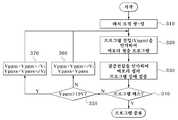
도 5는 본 발명의 일 실시예에 따른 낸드 플래시 메모리소자의 프로그램 방법을 나타내는 플로 차트(flow chart)이다.FIG. 5 is a flowchart illustrating a program method of a NAND flash memory device according to an exemplary embodiment of the present invention.
도 5를 참조하면, 먼저 래치 로직을 셋-업(set-up)시킨다(단계 310). 여기서 래치 로직은 메모리 셀에 적절한 바이어스를 인가하고 메모리 셀의 데이터를 저장 및 래치하기 위한 제어회로, 예컨대 페이지 버퍼를 포함한다. 이 과정에서 페이지 버퍼 내의 레지스터에는 프로그램 데이터를 포함하는 데이터의 래치가 이루어진다. 데이터 래치가 이루어지면, 프로그램될 메모리 셀이 연결된 워드라인에 프로그램 전압(Vpgm)을 인가하여 메모리 셀을 프로그램한다(단계 320). 이때, 선택되지 않은 메모리 셀의 워드라인에는, 선택되지 않은 메모리 셀이 원치않게 프로그램되는 것 을 방지하기 위하여 패스전압(Vpass) 전압을 인가한다. 패스전압(Vpass)은 선택되지 않은 메모리 셀이 프로그램되는 것을 방지할 수 있는 정도의 크기, 예를 들어 7.0 ∼ 11.0V 내에서 적절한 크기로 선택할 수 있다.Referring to FIG. 5, first, the latch logic is set up (step 310). The latch logic here includes a control circuit, such as a page buffer, for applying an appropriate bias to the memory cell and for storing and latching data in the memory cell. In this process, data including program data is latched to a register in the page buffer. When the data latch is performed, the memory cell is programmed by applying a program voltage Vpgm to a word line to which the memory cell to be programmed is connected (step 320). At this time, a pass voltage Vpass is applied to the word lines of the unselected memory cells in order to prevent unwanted programming of the unselected memory cells. The pass voltage Vpass may be selected to an appropriate size within a magnitude that can prevent the unselected memory cells from being programmed, for example, 7.0 to 11.0V.
메모리 셀을 프로그램한 다음에는 검증전압을 인가하여, 선택된 메모리 셀이 원하는 레벨로 프로그램되었는지를 검증한다(단계 330). 검증결과 모든 메모리 셀이 프로그램 단계를 패스하였는지를 판단하고(단계 340), 프로그램 단계를 패스하였으면 프로그램 동작을 종료한다.After programming the memory cell, a verification voltage is applied to verify whether the selected memory cell has been programmed to a desired level (step 330). As a result of the verification, it is determined whether all the memory cells have passed the program step (step 340). If the program step passes, the program operation is terminated.
검증결과, 적정한 레벨로 프로그램되지 못한 메모리 셀이 존재하여 프로그램 단계를 패스하지 못했다면 프로그램 전압(Vpgm)을 일정 스텝전압(△V1) 만큼 증가시켜 다시 프로그램하는데, 그 전에 프로그램 전압(Vpgm)이 소정 레벨, 예를 들어 19V를 넘어섰는지 확인한다(단계 350). 이는, 앞서 설명한 바와 같이 프로그램 전압이 증가함에 따라 채널 부스팅 레벨이 감소하는 것을 방지하기 위한 것으로, 프로그램 전압(Vpgm)이 일정 크기 이상이 되면 패스전압(Vpass)도 일정 크기만큼 증가시키기 위한 것이다.As a result of the verification, if there is a memory cell that is not programmed at the proper level and the program step is not passed, the program voltage Vpgm is increased by a predetermined step voltage ΔV1 and reprogrammed. It is checked if it is above a predetermined level, for example 19V (step 350). This is to prevent the channel boosting level from decreasing as the program voltage increases as described above, and to increase the pass voltage Vpass by a certain amount when the program voltage Vpgm becomes greater than or equal to a certain amount.
메모리 셀의 워드라인에 공급한 프로그램 전압(Vpgm)이 설정된 레벨, 예를 들어 19V 보다 큰 경우, 프로그램 전압(Vpgm)을 제1 스텝전압(△V1)만큼 증가시킴과 동시에 선택되지 않은 메모리 셀에 인가하는 패스전압(Vpass)도 제2 스텝전압(△V2)만큼 증가시킨다(단계 370). 제1 및 제2 스텝전압의 크기가 클수록 프로그램 속도는 빠르지만 메모리 셀의 문턱전압 분포의 폭이 넓어지므로, 프로그램 속도와 문턱 전압 분포의 폭을 고려하여 적절한 크기로 결정할 수 있다. 그리고, 제2 스텝전압(△V2)은 제1 스텝전압(△V1)보다 작거나 같을 수 있다. 바람직한 실시예에서, 상기 제2 스텝전압(△V2)은 0.2 ∼ 1.0V 정도일 수 있다.Level, the program voltage (Vpgm) supplied to the word lines of the memory cell is set, for example, is greater than 19V, the program voltage (Vpgm) by a first step voltage (△ V1) memory cells are not selected at the same time increasing as The pass voltage Vpass to be applied also increases by the second step voltage DELTA V2 (step 370). The larger the first and second step voltages are, the faster the program speed is, but the width of the threshold voltage distribution of the memory cell is wider, so that an appropriate size may be determined in consideration of the program speed and the width of the threshold voltage distribution. The second step voltage ΔV2 may be less than or equal to the first step voltage ΔV1 . In a preferred embodiment, the second step voltage (△ V2) can be on the order of 0.2 ~ 1.0V.
메모리 셀의 워드라인에 공급한 프로그램 전압(Vpgm)이 설정된 레벨, 예를 들어 19V보다 크지 않을 경우에는 패스전압(Vpass)의 증가없이 프로그램 전압(Vpgm)만 제1 스텝전압(△V1)만큼 증가시켜(단계 360), 메모리 셀을 프로그램하고 검증하는 동작을 프로그램 단계를 패스할 때까지 정해진 루프(loop) 내에서 반복한다.Level, the program voltage (Vpgm) supplied to the word lines of the memory cell is set, for example, as it is not more than 19V, only the program voltage (Vpgm) without increasing the pass voltage (Vpass) a first step voltage (△ V1) Incrementally (step 360), the operation of programming and verifying the memory cells is repeated in a predetermined loop until the program step passes.
이와 같이, 선택된 메모리 셀에 인가하는 프로그램 전압(Vpgm)에 따라서 패스전압(Vpass)도 변동되도록 함으로써, 채널의 부스팅 레벨을 증가시켜 프로그램 디스터브를 줄일 수 있으며, 따라서 메모리 셀의 문턱전압 분포를 좁게 하여 소자의 동작특성을 향상시킬 수 있다.As such, the pass voltage Vpass also varies according to the program voltage Vpgm applied to the selected memory cell, thereby increasing the channel boosting level, thereby reducing program disturb, thereby narrowing the threshold voltage distribution of the memory cell. The operation characteristics of the device can be improved.
한편, 선택되지 않은 메모리 셀에 인가하는 패스전압(Vpass)은 일정 프로그램 루프(loop) 이후부터 증가시킬 수 있다. 즉, 일정 프로그램 루프를 돌고 난 이후부터 패스전압(Vpass)이 일정 스텝전압만큼 증가하도록 할 수 있다.Meanwhile, the pass voltage Vpass applied to the unselected memory cells may increase after a predetermined program loop. That is, after the constant program loop, the pass voltage Vpass may be increased by a predetermined step voltage.
도 6은 본 발명의 다른 실시예에 따른 플래시 메모리소자의 프로그램 방법을 설명하기 위한 도면으로, 일정 프로그램 루프 이후부터 패스전압을 증가시키는 경우를 나타내는 플로차트이다.FIG. 6 is a flowchart illustrating a program method of a flash memory device according to another exemplary embodiment of the present invention, and is a flowchart illustrating a case in which a pass voltage is increased after a predetermined program loop.
도 6을 참조하면, 먼저 래치 로직을 셋-업시키고(단계 410), 프로그램될 메 모리 셀이 연결된 워드라인에 프로그램 전압(Vpgm)을 인가하여 메모리 셀을 프로그램한다(단계 420). 이때, 선택되지 않은 메모리 셀의 워드라인에는, 선택되지 않은 메모리 셀이 원치않게 프로그램되는 것을 방지하기 위하여 패스전압(Vpass)을 인가한다. 패스전압(Vpass)은 선택되지 않은 메모리 셀이 프로그램되는 것을 방지할 수 있는 정도의 크기, 예를 들어 7.0 ∼ 11.0V 내에서 적절한 크기로 선택할 수 있다.Referring to FIG. 6, first, the latch logic is set up (step 410), and a memory cell is programmed by applying a program voltage Vpgm to a word line to which a memory cell to be programmed is connected (step 420). At this time, a pass voltage Vpass is applied to the word lines of the unselected memory cells in order to prevent unselected memory cells from being programmed undesirably. The pass voltage Vpass may be selected to an appropriate size within a magnitude that can prevent the unselected memory cells from being programmed, for example, 7.0 to 11.0V.
메모리 셀을 프로그램한 다음에는 검증전압을 인가하여, 선택된 메모리 셀이 원하는 레벨로 프로그램되었는지를 검증한다(단계 430). 검증결과, 모든 메모리 셀이 프로그램 단계를 패스하였는지를 판단하고(단계 440), 프로그램 단계를 패스하였으면 프로그램 동작을 종료한다.After programming the memory cell, a verification voltage is applied to verify whether the selected memory cell has been programmed to a desired level (step 430). As a result of the verification, it is determined whether all the memory cells have passed the program step (step 440). If the program step has passed, the program operation is terminated.
검증결과, 프로그램 단계를 패스하지 못했다면, 즉 적정한 레벨로 프로그램되지 못한 메모리 셀이 존재할 경우 프로그램 전압(Vpgm)을 일정 스텝전압(△V1) 만큼 증가시켜 다시 프로그램하는데, 그 전에 채널의 부스팅 레벨의 감소를 방지하기 위하여 프로그램 루프(loop)가 일정 횟수, 예를 들어 8회가 수행되었는지를 확인한다(단계 450). 프로그램 루프가 8회 수행되어 9번째 프로그램 펄스를 인가할 단계인 경우, 프로그램 전압(Vpgm)을 제1 스텝전압(△V1)만큼 증가시킴과 동시에 선택되지 않은 메모리 셀에 인가하는 패스전압(Vpass)도 제2 스텝전압(△V2)만큼 증가시킨다(단계 470).As a result of the verification, if the program step is not passed, that is, if there is a memory cell that has not been programmed to an appropriate level, the program voltage Vpgm is increased by a predetermined step voltage ΔV1 and reprogrammed. In order to prevent the decrease of the program loop, it is checked whether a predetermined number of times, for example, eight times, has been performed (step 450). Program loop is performed eight times ninth program if the step of applying the pulse, the program voltage (Vpgm) by a first step voltage (△ V1) applying a pass voltage (Vpass to the non-increase Sikkim and at the same time be selected memory cell by Also increases by the second step voltage DELTA V2 (step 470).
제1 및 제2 스텝전압의 크기는 프로그램 속도와 문턱전압의 분포 폭을 고려하여 적절한 크기로 결정할 수 있다. 제2 스텝전압(△V2)은 제1 스텝전압(△V1)보다 작거나 같을 수 있는데, 제2 스텝전압(△V2)은 0.2 ∼ 1.0V 정도일 수 있다. 그리고, 패스전압(Vpass)을 증가시키는 프로그램 루프의 수는 8회로 고정되는 것이 아니라, 메모리 소자의 특성에 따라 결정할 수 있다.The magnitudes of the first and second step voltages may be appropriately determined in consideration of the program speed and the distribution width of the threshold voltage. A second step voltage (△ V2) there is a number less than or equal to the first voltage step (△ V1), the second voltage may be on the order of step (△ V2) is 0.2 ~ 1.0V. The number of program loops for increasing the pass voltage Vpass is not fixed to eight, but may be determined according to the characteristics of the memory device.
한편, 멀티 레벨 셀 구조의 플래시 메모리소자의 경우에는 하위비트(LSB)와 상위비트(MSB)로 이루어져 하위비트(LSB)의 프로그램 상태에 따라 상위비트(MSB)의 프로그램을 수행하게 된다. 하위비트(LSB) 및 상위비트(MSB)를 ISPP 방식으로 프로그램할 경우에도, 상술한 본 발명의 프로그램 방법을 적용하여 프로그램 전압(Vpgm) 또는 프로그램 루프에 따라, 선택되지 않은 메모리 셀의 워드라인에 인가하는 패스전압(Vpass)을 적절한 크기로 증가시키면 프로그램 디스터브를 줄이거나 혹은 방지할 수 있다. 이 경우에도, 제1 스텝전압과 제2 스텝전압의 크기는 프로그램 속도와 문턱전압의 분포 폭을 고려하여 적절한 크기로 결정할 수 있다. 제2 스텝전압(△V2)은 제1 스텝전압(△V1)보다 작거나 같을 수 있는데, 제2 스텝전압(△V2)은 0.2 ∼ 1.0V 정도일 수 있다. 또는, 하위비트(LSB) 또는 상위비트(MSB) 프로그램 동작에서의 프로그램 검증전압의 크기에 따라 패스전압(Vpass)의 크기를 증가시킬 수도 있다.On the other hand, in the case of a flash memory device having a multi-level cell structure, the lower bit LSB and the upper bit MSB are used to program the upper bit MSB according to the program state of the lower bit LSB. Even when the lower bit LSB and the upper bit MSB are programmed in the ISPP method, the above-described programming method of the present invention is applied to the word lines of the unselected memory cells according to the program voltage Vpgm or the program loop. Increasing the applied pass voltage Vpass to an appropriate magnitude can reduce or prevent program disturb. Even in this case, the magnitudes of the first step voltage and the second step voltage may be determined to be appropriate in consideration of the program speed and the distribution width of the threshold voltage. A second step voltage (△ V2) there is a number less than or equal to the first voltage step (△ V1), the second voltage may be on the order of step (△ V2) is 0.2 ~ 1.0V. Alternatively, the magnitude of the pass voltage Vpass may be increased according to the magnitude of the program verify voltage in the lower bit LSB or upper bit MSB program operation.
이상 본 발명을 바람직한 실시예를 들어 상세하게 설명하였으나, 본 발명은 상기 실시예에 한정되지 않으며, 본 발명의 기술적 사상 내에서 당 분야에서 통상의 지식을 가진 자에 의하여 여러 가지 변형이 가능함은 당연하다.Although the present invention has been described in detail with reference to preferred embodiments, the present invention is not limited to the above embodiments, and various modifications may be made by those skilled in the art within the technical spirit of the present invention. Do.
도 1은 낸드 플래시 메모리소자의 셀 스트링과 페이지 버퍼의 구조를 나타낸 도면이다.1 is a diagram illustrating the structure of a cell string and a page buffer of a NAND flash memory device.
도 2는 셀프 부스팅 프로그램 방식의 타이밍도이다.2 is a timing diagram of a self-boosting program method.
도 3은 낸드 플래시 메모리소자의 프로그램 동작시의 셀 스트링의 회로모델을 나타낸 도면이다.3 is a diagram illustrating a circuit model of a cell string during a program operation of a NAND flash memory device.
도 4는 본 발명에 따른 플래시 메모리소자의 프로그램 동작시의 프로그램 전압 및 패스전압의 변화를 나타낸 도면이다.4 is a diagram illustrating a change in a program voltage and a pass voltage during a program operation of a flash memory device according to the present invention.
도 5는 본 발명의 일 실시예에 따른 낸드 플래시 메모리소자의 프로그램 방법을 나타내는 흐름도이다.5 is a flowchart illustrating a program method of a NAND flash memory device according to an exemplary embodiment of the present invention.
도 6은 본 발명의 다른 실시예에 따른 낸드 플래시 메모리소자의 프로그램 방법을 나타내는 흐름도이다.6 is a flowchart illustrating a program method of a NAND flash memory device according to another exemplary embodiment of the present invention.
Claims (16)
Translated fromKoreanPriority Applications (3)
| Application Number | Priority Date | Filing Date | Title |
|---|---|---|---|
| KR1020080033603AKR101076879B1 (en) | 2008-04-11 | 2008-04-11 | Method of programming flash memory device using self boosting |
| US12/422,184US8027202B2 (en) | 2008-04-11 | 2009-04-10 | Method of programming a flash memory device using self boosting |
| CN2009101337825ACN101556827B (en) | 2008-04-11 | 2009-04-13 | Method of programming a flash memory device using self boosting |
Applications Claiming Priority (1)
| Application Number | Priority Date | Filing Date | Title |
|---|---|---|---|
| KR1020080033603AKR101076879B1 (en) | 2008-04-11 | 2008-04-11 | Method of programming flash memory device using self boosting |
Publications (2)
| Publication Number | Publication Date |
|---|---|
| KR20090108267A KR20090108267A (en) | 2009-10-15 |
| KR101076879B1true KR101076879B1 (en) | 2011-10-25 |
Family
ID=41163863
Family Applications (1)
| Application Number | Title | Priority Date | Filing Date |
|---|---|---|---|
| KR1020080033603AActiveKR101076879B1 (en) | 2008-04-11 | 2008-04-11 | Method of programming flash memory device using self boosting |
Country Status (3)
| Country | Link |
|---|---|
| US (1) | US8027202B2 (en) |
| KR (1) | KR101076879B1 (en) |
| CN (1) | CN101556827B (en) |
Cited By (1)
| Publication number | Priority date | Publication date | Assignee | Title |
|---|---|---|---|---|
| US12068045B2 (en) | 2021-08-17 | 2024-08-20 | SK Hynix Inc. | Semiconductor memory device and operating method thereof |
Families Citing this family (32)
| Publication number | Priority date | Publication date | Assignee | Title |
|---|---|---|---|---|
| EP2279253B1 (en) | 2008-04-09 | 2016-11-16 | Maxcyte, Inc. | Engineering and delivery of therapeutic compositions of freshly isolated cells |
| KR101468097B1 (en)* | 2008-09-18 | 2014-12-04 | 삼성전자주식회사 | Memory device and its programming method |
| US8355286B2 (en)* | 2009-05-08 | 2013-01-15 | Hynix Semiconductor Inc. | Method of operating nonvolatile memory device controlled by controlling coupling resistance value between a bit line and a page buffer |
| US20110149667A1 (en)* | 2009-12-23 | 2011-06-23 | Fatih Hamzaoglu | Reduced area memory array by using sense amplifier as write driver |
| US8982631B2 (en)* | 2010-02-09 | 2015-03-17 | Micron Technology, Inc. | Programming methods and memories |
| US9107878B2 (en) | 2010-04-06 | 2015-08-18 | Exocyte Therapeutics Pte, Ltd | Methods of treating cancer |
| KR101134240B1 (en)* | 2010-04-29 | 2012-04-09 | 주식회사 하이닉스반도체 | Method for operating a semiconductor memory apparatus |
| US8369149B2 (en) | 2010-09-30 | 2013-02-05 | Sandisk Technologies Inc. | Multi-step channel boosting to reduce channel to floating gate coupling in memory |
| US8854891B2 (en)* | 2011-07-06 | 2014-10-07 | SK Hynix Inc. | Method of operating semiconductor device |
| KR20130044693A (en)* | 2011-10-24 | 2013-05-03 | 에스케이하이닉스 주식회사 | Semiconductor memory device and method of the same |
| TWI582778B (en)* | 2011-12-09 | 2017-05-11 | Toshiba Kk | Nonvolatile semiconductor memory device |
| TWI456575B (en)* | 2011-12-30 | 2014-10-11 | Macronix Int Co Ltd | Method for programming memory array |
| KR102016036B1 (en)* | 2012-08-30 | 2019-08-29 | 에스케이하이닉스 주식회사 | Semiconductor memory device and method of operating the same |
| KR102022502B1 (en)* | 2012-08-30 | 2019-09-18 | 에스케이하이닉스 주식회사 | Programming method of nonvolatile memory device |
| TWI496148B (en)* | 2013-02-08 | 2015-08-11 | Macronix Int Co Ltd | Method of programming flash memory |
| US9224470B1 (en)* | 2014-08-05 | 2015-12-29 | Taiwan Semiconductor Manufacturing Company, Ltd. | Memory circuit and method of programming memory circuit |
| KR102272238B1 (en)* | 2014-09-02 | 2021-07-06 | 삼성전자주식회사 | Nonvolatile memory device and programming method thereof |
| CN106486161B (en)* | 2015-08-24 | 2019-12-13 | 北京兆易创新科技股份有限公司 | Anti-interference method for NANDFLASH programming |
| KR102395727B1 (en)* | 2016-04-25 | 2022-05-10 | 에스케이하이닉스 주식회사 | Semiconductor memory device and operating method thereof |
| KR102461726B1 (en)* | 2016-07-19 | 2022-11-02 | 에스케이하이닉스 주식회사 | Memory device and operating method thereof |
| KR102533016B1 (en) | 2016-07-28 | 2023-05-17 | 에스케이하이닉스 주식회사 | Memory device and operating method thereof |
| KR102634418B1 (en)* | 2016-12-07 | 2024-02-06 | 에스케이하이닉스 주식회사 | Semiconductor memory device and operating method thereof |
| JP2018113084A (en)* | 2017-01-06 | 2018-07-19 | 東芝メモリ株式会社 | Semiconductor memory device |
| TWI695385B (en)* | 2019-05-31 | 2020-06-01 | 旺宏電子股份有限公司 | Non-volatile memory and operating method thereof |
| CN110580928B (en)* | 2019-08-09 | 2021-08-17 | 长江存储科技有限责任公司 | A three-dimensional memory control method, device and storage medium |
| EP3877978B1 (en) | 2019-08-28 | 2023-07-12 | Yangtze Memory Technologies Co., Ltd. | Method of programming in flash memory devices |
| JP7132444B2 (en) | 2019-12-09 | 2022-09-06 | 長江存儲科技有限責任公司 | Method for reducing program disturbance in memory device and memory device using the same |
| US12412609B2 (en) | 2019-12-09 | 2025-09-09 | Yangtze Memory Technologies Co., Ltd. | Method of reducing program disturbance in memory device and memory device utilizing same |
| CN113823347A (en)* | 2020-04-15 | 2021-12-21 | 长江存储科技有限责任公司 | 3D NAND flash memory and operation method thereof |
| KR102816494B1 (en) | 2020-10-26 | 2025-06-04 | 삼성전자주식회사 | Nonvolatile memory devices and methods of programming in nonvolatile memory devices |
| US11894059B2 (en)* | 2021-07-28 | 2024-02-06 | SK Hynix Inc. | Apparatus and method for programming data in a non-volatile memory device |
| KR102832532B1 (en) | 2021-10-30 | 2025-07-09 | 양쯔 메모리 테크놀로지스 씨오., 엘티디. | Memory devices and their program operation |
Citations (2)
| Publication number | Priority date | Publication date | Assignee | Title |
|---|---|---|---|---|
| KR100764053B1 (en)* | 2006-08-10 | 2007-10-08 | 삼성전자주식회사 | Flash memory device and its program method |
| US20080049494A1 (en)* | 2006-08-22 | 2008-02-28 | Micron Technology, Inc. | Reducing effects of program disturb in a memory device |
Family Cites Families (5)
| Publication number | Priority date | Publication date | Assignee | Title |
|---|---|---|---|---|
| US6859397B2 (en)* | 2003-03-05 | 2005-02-22 | Sandisk Corporation | Source side self boosting technique for non-volatile memory |
| KR20040086669A (en) | 2003-04-03 | 2004-10-12 | 주식회사 소프텔레웨어 | Service System And Method For Completion Of Calls In Mobile Communication Network |
| US7379333B2 (en)* | 2004-10-28 | 2008-05-27 | Samsung Electronics Co., Ltd. | Page-buffer and non-volatile semiconductor memory including page buffer |
| US7230854B2 (en)* | 2005-08-01 | 2007-06-12 | Sandisk Corporation | Method for programming non-volatile memory with self-adjusting maximum program loop |
| US7440326B2 (en)* | 2006-09-06 | 2008-10-21 | Sandisk Corporation | Programming non-volatile memory with improved boosting |
- 2008
- 2008-04-11KRKR1020080033603Apatent/KR101076879B1/enactiveActive
- 2009
- 2009-04-10USUS12/422,184patent/US8027202B2/enactiveActive
- 2009-04-13CNCN2009101337825Apatent/CN101556827B/enactiveActive
Patent Citations (2)
| Publication number | Priority date | Publication date | Assignee | Title |
|---|---|---|---|---|
| KR100764053B1 (en)* | 2006-08-10 | 2007-10-08 | 삼성전자주식회사 | Flash memory device and its program method |
| US20080049494A1 (en)* | 2006-08-22 | 2008-02-28 | Micron Technology, Inc. | Reducing effects of program disturb in a memory device |
Cited By (1)
| Publication number | Priority date | Publication date | Assignee | Title |
|---|---|---|---|---|
| US12068045B2 (en) | 2021-08-17 | 2024-08-20 | SK Hynix Inc. | Semiconductor memory device and operating method thereof |
Also Published As
| Publication number | Publication date |
|---|---|
| CN101556827A (en) | 2009-10-14 |
| CN101556827B (en) | 2013-01-30 |
| US20090257281A1 (en) | 2009-10-15 |
| US8027202B2 (en) | 2011-09-27 |
| KR20090108267A (en) | 2009-10-15 |
Similar Documents
| Publication | Publication Date | Title |
|---|---|---|
| KR101076879B1 (en) | Method of programming flash memory device using self boosting | |
| US7672166B2 (en) | Method of programming in a non-volatile memory device and non-volatile memory device for performing the same | |
| CN101361134B (en) | Method for programming non-volatile memory with reduced program disturb using modified pass voltages and storage system | |
| TWI453748B (en) | Flash memory program inhibit scheme | |
| US8902659B2 (en) | Shared-bit-line bit line setup scheme | |
| CN100511483C (en) | Non-volatile memory device and method of preventing hot electron program disturb phenomenon | |
| JP5279729B2 (en) | Source side asymmetric precharge program method | |
| EP1599881B1 (en) | Nand flash memory avoiding program disturb with a self boosting technique | |
| KR100502412B1 (en) | Non-volatile semiconductor memory device and program method thereof | |
| EP2446443B1 (en) | Forecasting program disturb in memory by detecting natural threshold voltage distribution | |
| US7508711B2 (en) | Arrangements for operating a memory circuit | |
| CN102760483B (en) | How to operate a semiconductor device | |
| US8050090B2 (en) | Memory page boosting method, device and system | |
| US8116140B2 (en) | Saw-shaped multi-pulse programming for program noise reduction in memory | |
| KR101102505B1 (en) | How to Program a Nonvolatile Memory Device | |
| KR101047168B1 (en) | Partitioned Soft Programming in Nonvolatile Memory | |
| KR100811277B1 (en) | Erasing Method of NAND Flash Memory Devices | |
| KR20090052507A (en) | How flash memory devices work | |
| KR20130006299A (en) | Operating method of semiconductor device | |
| KR20100115114A (en) | Method of programming a non volatile memory device | |
| KR20080041479A (en) | Data erasing method of NAND flash memory device | |
| KR20110001064A (en) | Program Method of Nonvolatile Memory Device |
Legal Events
| Date | Code | Title | Description |
|---|---|---|---|
| PA0109 | Patent application | Patent event code:PA01091R01D Comment text:Patent Application Patent event date:20080411 | |
| A201 | Request for examination | ||
| PA0201 | Request for examination | Patent event code:PA02012R01D Patent event date:20090811 Comment text:Request for Examination of Application Patent event code:PA02011R01I Patent event date:20080411 Comment text:Patent Application | |
| PG1501 | Laying open of application | ||
| E902 | Notification of reason for refusal | ||
| PE0902 | Notice of grounds for rejection | Comment text:Notification of reason for refusal Patent event date:20110112 Patent event code:PE09021S01D | |
| E701 | Decision to grant or registration of patent right | ||
| PE0701 | Decision of registration | Patent event code:PE07011S01D Comment text:Decision to Grant Registration Patent event date:20110729 | |
| GRNT | Written decision to grant | ||
| PR0701 | Registration of establishment | Comment text:Registration of Establishment Patent event date:20111019 Patent event code:PR07011E01D | |
| PR1002 | Payment of registration fee | Payment date:20111020 End annual number:3 Start annual number:1 | |
| PG1601 | Publication of registration | ||
| FPAY | Annual fee payment | Payment date:20140923 Year of fee payment:4 | |
| PR1001 | Payment of annual fee | Payment date:20140923 Start annual number:4 End annual number:4 | |
| FPAY | Annual fee payment | Payment date:20150921 Year of fee payment:5 | |
| PR1001 | Payment of annual fee | Payment date:20150921 Start annual number:5 End annual number:5 | |
| FPAY | Annual fee payment | Payment date:20160923 Year of fee payment:6 | |
| PR1001 | Payment of annual fee | Payment date:20160923 Start annual number:6 End annual number:6 | |
| FPAY | Annual fee payment | Payment date:20170925 Year of fee payment:7 | |
| PR1001 | Payment of annual fee | Payment date:20170925 Start annual number:7 End annual number:7 | |
| FPAY | Annual fee payment | Payment date:20180920 Year of fee payment:8 | |
| PR1001 | Payment of annual fee | Payment date:20180920 Start annual number:8 End annual number:8 | |
| PR1001 | Payment of annual fee | Payment date:20200924 Start annual number:10 End annual number:10 | |
| PR1001 | Payment of annual fee | Payment date:20220926 Start annual number:12 End annual number:12 | |
| PR1001 | Payment of annual fee |