KR101076813B1 - Semiconductor Device and Method for Manufacturing the same - Google Patents
Semiconductor Device and Method for Manufacturing the sameDownload PDFInfo
- Publication number
- KR101076813B1 KR101076813B1KR1020090053947AKR20090053947AKR101076813B1KR 101076813 B1KR101076813 B1KR 101076813B1KR 1020090053947 AKR1020090053947 AKR 1020090053947AKR 20090053947 AKR20090053947 AKR 20090053947AKR 101076813 B1KR101076813 B1KR 101076813B1
- Authority
- KR
- South Korea
- Prior art keywords
- storage node
- node contact
- semiconductor device
- forming
- region
- Prior art date
- Legal status (The legal status is an assumption and is not a legal conclusion. Google has not performed a legal analysis and makes no representation as to the accuracy of the status listed.)
- Expired - Fee Related
Links
Images


Classifications
- H—ELECTRICITY
- H10—SEMICONDUCTOR DEVICES; ELECTRIC SOLID-STATE DEVICES NOT OTHERWISE PROVIDED FOR
- H10B—ELECTRONIC MEMORY DEVICES
- H10B12/00—Dynamic random access memory [DRAM] devices
- H10B12/01—Manufacture or treatment
- H10B12/02—Manufacture or treatment for one transistor one-capacitor [1T-1C] memory cells
- H10B12/03—Making the capacitor or connections thereto
- H10B12/033—Making the capacitor or connections thereto the capacitor extending over the transistor
- H10B12/0335—Making a connection between the transistor and the capacitor, e.g. plug
- H—ELECTRICITY
- H01—ELECTRIC ELEMENTS
- H01L—SEMICONDUCTOR DEVICES NOT COVERED BY CLASS H10
- H01L21/00—Processes or apparatus adapted for the manufacture or treatment of semiconductor or solid state devices or of parts thereof
- H01L21/70—Manufacture or treatment of devices consisting of a plurality of solid state components formed in or on a common substrate or of parts thereof; Manufacture of integrated circuit devices or of parts thereof
- H01L21/71—Manufacture of specific parts of devices defined in group H01L21/70
- H01L21/768—Applying interconnections to be used for carrying current between separate components within a device comprising conductors and dielectrics
- H01L21/76897—Formation of self-aligned vias or contact plugs, i.e. involving a lithographically uncritical step
- H—ELECTRICITY
- H10—SEMICONDUCTOR DEVICES; ELECTRIC SOLID-STATE DEVICES NOT OTHERWISE PROVIDED FOR
- H10B—ELECTRONIC MEMORY DEVICES
- H10B12/00—Dynamic random access memory [DRAM] devices
- H10B12/30—DRAM devices comprising one-transistor - one-capacitor [1T-1C] memory cells
- H10B12/48—Data lines or contacts therefor
- H10B12/482—Bit lines
Landscapes
- Engineering & Computer Science (AREA)
- Manufacturing & Machinery (AREA)
- Physics & Mathematics (AREA)
- Condensed Matter Physics & Semiconductors (AREA)
- General Physics & Mathematics (AREA)
- Computer Hardware Design (AREA)
- Microelectronics & Electronic Packaging (AREA)
- Power Engineering (AREA)
- Internal Circuitry In Semiconductor Integrated Circuit Devices (AREA)
- Semiconductor Memories (AREA)
Abstract
Translated fromKoreanDescription
Translated fromKorean본 발명은 반도체 소자 및 그 제조 방법에 관한 것으로, 특히 고집적 반도체 소자를 제조함에 있어서 스토리지노드 콘택의 마진 확보와 비트 라인과의 쇼트를 방지할 수 있는 반도체 소자 및 그 제조 방법에 관련된 기술이다.BACKGROUND OF THE INVENTION 1. Field of the Invention The present invention relates to a semiconductor device and a method of manufacturing the same, and more particularly, to a semiconductor device and a method of manufacturing the same, which can prevent a margin of a storage node contact and a short circuit with a bit line in manufacturing a highly integrated semiconductor device.
반도체는 전기 전도도에 따른 물질의 분류 가운데 하나로 도체와 부도체의 중간 영역에 속하는 물질로서, 반도체에 불순물을 첨가하고 도체를 연결하여 트랜지스터와 같은 반도체 소자를 생성하는데 사용된다. 이러한 반도체 소자를 이용하여 데이터 저장 등의 여러 가지 기능을 수행하는 장치를 반도체 장치라 한다.A semiconductor is a class of materials according to electrical conductivity, and is a material belonging to an intermediate region of a conductor and a non-conductor. The semiconductor is used to add semiconductor impurities and connect conductors to create semiconductor devices such as transistors. A device that performs various functions such as data storage using such a semiconductor device is called a semiconductor device.
이러한 반도체 장치가 점점 고집적화되면서 반도체 칩 크기가 감소하고, 이에 따라 칩 내에 형성되는 다수의 반도체 소자의 크기도 감소하게 되었다.As the semiconductor devices are increasingly integrated, semiconductor chip sizes are reduced, and thus, the size of a plurality of semiconductor devices formed in the chip is also reduced.
도 1은 종래 기술에 따른 반도체 소자의 제조 방법을 도시한 평면도이다.1 is a plan view illustrating a method of manufacturing a semiconductor device according to the prior art.
도 1을 참조하면, 반도체 기판(100)상에 바(Bar) 형의 6F2 구조의 활성 영역(110)이 아일랜드(Island) 타입으로 배열되어 정의되고, 활성 영역(110) 사이의 영역에 소자분리막(미도시)이 형성된다.Referring to FIG. 1, an
다음에는, 활성 영역(110)의 길이 방향에 대하여 비스듬한 방향으로 교차하는 게이트(120)가 형성된다. 복수의 게이트(120)는 하나의 활성 영역(110)을 3등분하되, 게이트(120) 사이에 노출되는 활성 영역(110)의 양 외곽 영역에는 각각 제 1 스토리지노드 콘택(130)이 형성되고 중심부에는 비트 라인 콘택(140)이 형성된다. 이때, 제 1 스토리지노드 콘택(130)은 홀 타입으로 형성되어있다.Next, a
다음에는, 상기 비트 라인 콘택(140)의 상부에는 비트 라인(150)이 형성된다. 이때, 비트 라인(150)은 라인(Line) 구조로 되어있다.Next, a
이후, 제 1 스토리지노드 콘택(130) 상부에는 제 2 스토리지노드 콘택(160)을 형성한다. 이때, 제 2 스토리지노드 콘택(160)은 홀(Hole) 타입으로 형성되어 있다.Thereafter, a second
전술한 반도체 소자의 제조 방법에서, 상기 제 1 및 제 2 스토리지노드 콘택은 모두 홀(Hole) 타입으로 형성하기 때문에 30nm 이하의 고집적화된 반도체 소자에서는 구현이 불가능하며, 스토리지노드 콘택(SNC)과 활성 영역의 오버랩 마진(Margin)을 개선하기 위하여 콘택의 CD(Critical Dimension)를 크게 형성하면 인접한 비트라인 콘택과 SAC(Self-aligned contact) 페일이 발생하는 문제점이 있다.In the above-described method of manufacturing a semiconductor device, since the first and second storage node contacts are all formed in a hole type, they cannot be implemented in a highly integrated semiconductor device of 30 nm or less, and the storage node contact (SNC) and the active In order to improve a region's overlap margin, if a CD is formed to have a large critical dimension, adjacent bit line contacts and self-aligned contact (SAC) fail may occur.
전술한 종래의 문제점을 해결하기 위하여, 본 발명은 서로 다른 상기 활성 영역의 양 외곽이 한 번에 노출되는 마스크를 이용하여 제 1 스토리지노드 콘택을 형성함으로써, 상기 제 1 스토리지노드 콘택과 상기 활성 영역의 오버랩 마진(Margin)을 확보할 수 있고, 상기 제 1 스토리지노드 콘택 상에 제 2 스토리지노드 콘택을 라인(Line) 타입으로 형성함으로써, 비트 라인 콘택과의 쇼트(Short)를 방지할 수 있으며, 상기 제 2 스토리지노드 콘택의 상부 CD(Critical Dimension)를 최대한 확보하여 후속 공정 중 형성되는 하부 전극과의 저항을 개선할 수 있는 반도체 소자 및 그 제조 방법을 제공한다.In order to solve the above-mentioned problems, the present invention forms a first storage node contact by using a mask in which both outer sides of the different active areas are exposed at one time, thereby forming the first storage node contact and the active area. It is possible to secure an overlap margin of, and by forming a second storage node contact in a line type on the first storage node contact, it is possible to prevent a short with the bit line contact. Provided are a semiconductor device and a method of manufacturing the same, which can improve resistance to a lower electrode formed during a subsequent process by securing the upper critical dimension of the second storage node contact to the maximum.
본 발명은 반도체 기판상에 형성된 홀(Hole) 구조의 제 1 스토리지 노드 콘택 및 상기 제 1 스토리지 노드 콘택 상에 형성된 라인(Line) 구조의 제 2 스토리지 노드 콘택을 포함하는 반도체 소자를 제공한다.The present invention provides a semiconductor device including a first storage node contact having a hole structure formed on a semiconductor substrate and a second storage node contact having a line structure formed on the first storage node contact.
아울러, 본 발명은 반도체 기판상에 활성 영역을 정의하는 소자분리막을 형성하는 단계, 상기 활성 영역을 포함한 전면에 절연막을 형성하는 단계, 제 1 스토리지노드 콘택 마스크를 이용하여 상기 절연막을 식각하여 제 1 스토리지노드 콘택 영역을 형성하는 단계, 상기 제 1 스토리지노드 콘택 영역에 도전 물질을 매립하여 제 1 스토리지노드 콘택을 형성하는 단계 및 상기 제 1 스토리지노드 콘택 상에 라인 구조의 제 2 스토리지노드 콘택을 형성하는 단계를 포함하는 반도체 소자의 제 조 방법을 제공한다.The present invention also provides a method of forming an isolation layer defining an active region on a semiconductor substrate, forming an insulating layer on the entire surface including the active region, and etching the insulating layer using a first storage node contact mask. Forming a storage node contact region, filling a conductive material in the first storage node contact region to form a first storage node contact, and forming a second storage node contact in a line structure on the first storage node contact It provides a method for manufacturing a semiconductor device comprising the step of.
바람직하게는, 상기 제 1 스토리지노드 콘택 마스크는 서로 다른 상기 활성 영역의 양 외곽이 한 번에 노출되도록 상기 절연막을 식각하는 것을 특징으로 한다.Preferably, the first storage node contact mask may etch the insulating layer so that both outer regions of different active regions are exposed at once.
바람직하게는, 상기 도전 물질을 매립한 후, 상기 도전 물질을 에치백(Etchback) 또는 평탄화 식각(Chemical Mechanical Polishing)하는 것을 더 포함한다.Preferably, the method further comprises embedding the conductive material, followed by etching or etching the conductive material.
바람직하게는, 상기 제 2 스토리지노드 콘택을 형성하는 단계는 상기 제 1 스토리지 노드 콘택 및 상기 절연막을 일부 식각하여 제 2 스토리지노드 콘택 영역을 형성하는 단계 및 상기 제 2 스토리지노드 콘택 영역에 도전 물질을 매립하는 것을 포함한다.The forming of the second storage node contact may include forming a second storage node contact region by partially etching the first storage node contact and the insulating layer, and forming a conductive material on the second storage node contact region. Involves landfilling.
본 발명은 서로 다른 상기 활성 영역의 양 외곽이 한 번에 노출되는 마스크를 이용하여 제 1 스토리지노드 콘택을 형성함으로써, 상기 제 1 스토리지노드 콘택과 상기 활성 영역의 오버랩 마진(Margin)을 확보할 수 있고, 상기 제 1 스토리지노드 콘택 상에 제 2 스토리지노드 콘택을 라인(Line) 타입으로 형성함으로써, 비트 라인 콘택과의 쇼트(Short)를 방지할 수 있으며, 상기 제 2 스토리지노드 콘택의 상부 CD(Critical Dimension)를 최대한 확보하여 후속 공정 중 형성되는 하부 전극과의 저항을 개선할 수 있는 장점이 있다.According to an exemplary embodiment of the present invention, a first storage node contact may be formed by using a mask in which two outer regions of different active regions are exposed at one time, thereby securing an overlap margin of the first storage node contact and the active region. In addition, by forming a second storage node contact in a line type on the first storage node contact, a short with a bit line contact can be prevented, and an upper CD of the second storage node contact Critical Dimension) has the advantage of improving the resistance with the lower electrode formed during the subsequent process to maximize the.
이하, 첨부한 도면을 참조하여 본 발명의 실시 예에 대해 상세히 설명하고자 한다.Hereinafter, with reference to the accompanying drawings will be described in detail an embodiment of the present invention.
도 2는 본 발명에 따른 반도체 소자의 제조 방법을 도시한 평면도이다.2 is a plan view illustrating a method of manufacturing a semiconductor device according to the present invention.
도 2를 참조하면, 반도체 기판(300)상에 바(Bar) 형의 6F2 구조의 활성 영역(310)이 아일랜드(Island) 타입으로 배열되어 정의되고, 활성 영역(310) 사이의 영역에 소자분리막(미도시)이 형성된다.Referring to FIG. 2, an
다음에는, 활성 영역(310)의 길이 방향에 대하여 비스듬한 방향으로 교차하는 게이트(320)가 형성된다. 복수의 게이트(320)는 하나의 활성 영역(310)을 3등분 하되, 게이트(320) 사이에 노출되는 활성 영역(310)의 양 외곽 영역에는 각각 제 1 스토리지노드 콘택(370)이 형성되고, 활셩 영역(310)의 중심부에는 비트 라인 콘택(340)이 형성된다. 이후, 상기 비트 라인 콘택(340)의 상부에는 상기 게이트(320)와 수직으로 교차하는 비트 라인(350)이 형성된다. 이때, 비트 라인(350)은 라인 구조가 바람직하다.Next, a
여기서, 제 1 스토리지노드 콘택(370) 형성 시, 도 2와 같이 서로 다른 활성 영역(310)의 외곽 영역을 한 번에 노출하는 타원형 마스크를 이용하는 것이 바람직하다.Here, when forming the first
이후, 제 1 스토리지노드 콘택(370) 상부에는 제 2 스토리지노드 콘택(380)을 형성한다. 이때, 제 2 스토리지노드 콘택(380)은 라인(Line) 구조로 형성하는 것이 바람직하다.Thereafter, a second
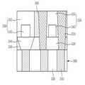
도 3a 내지 도 3d는 본 발명에 따른 반도체 소자의 형성 방법을 도시한 단면 도들로서, 도 2의 A-A' 절단면을 도시한 것이다.3A to 3D are cross-sectional views illustrating a method of forming a semiconductor device in accordance with the present invention, and illustrate a cross-sectional view taken along line A-A 'of FIG.
도 3a를 참조하면, 반도체 기판(300)상에 활성 영역(310)을 정의하는 소자분리막(320)을 형성한다. 이때, 소자분리막(320)은 STI(Shallow trench isolation) 공정을 통해 HDP(High density plasma) 산화막으로 형성하는 것이 바람직하다. 도시되지는 않았지만, 소자분리막(320)을 포함하는 전체 표면상에 감광막을 형성한 후, 리세스 마스크를 이용한 노광 및 현상 공정으로 감광막 패턴을 형성한다. 감광막 패턴을 마스크를 사용하여 활성 영역(310) 및 소자분리막(320)을 식각하여 리세스를 형성한다. 상기 리세스에 도전 물질을 매립하여 매립 게이트(미도시)를 형성한다.Referring to FIG. 3A, an
다음에는, 상기 매립 게이트를 포함한 전면에 제 1 층간 절연막(330)을 형성한 후, 상기 제 1 층간 절연막(330)을 식각하여 상기 활성 영역(310)을 노출하는 비트 라인 콘택 영역(미도시)을 형성한다. 이후, 비트 라인 콘택 영역에 도전 물질을 매립한 후, 평탄화 식각하여 비트 라인 콘택(340)을 완성한다.Next, after forming the first
다음에는, 상기 비트 라인 콘택(340) 상에 도전층(345) 및 하드마스크층(355)으로 구성된 비트 라인(350)을 형성한다.Next, a
다음에는, 상기 비트 라인(350)을 포함한 전면에 제 2 층간 절연막(360)을 형성한다. 이후, 제 2 층간 절연막(360) 상에 감광막을 형성한 후, 제 1 스토리지 노드 콘택 마스크를 이용한 노광 및 현상 공정으로 감광막 패턴(미도시)을 형성한다. 감광막 패턴을 마스크로 상기 활성 영역(310)이 노출될 때까지 상기 제 2 층간 절연막(360) 및 제 1 층간 절연막(330)을 식각하여 제 1 스토리지노드 콘택 영역 (미도시)을 형성한다. 이때, 제 1 스토리지노드 콘택 마스크는 상기 제 1 스토리지노드 콘택 영역을 형성하기 위해서 이용하되, 기존의 홀(Hole) 타입이 아닌 서로 다른 활성 영역(310)의 외곽 영역을 한 번에 노출하는 타원형이 바람직하다.Next, a second
여기서, 제 1 스토리지노드 콘택 마스크를 이용하여 상기 활성 영역(310)이 노출될 때까지 제 2 및 제 1 층간 절연막(360, 330)을 식각 시, 하부의 비트 라인(350)은 하드마스크층(355)으로 둘러싸여 있기 때문에 상기 하드마스크층(355)과 상기 층간 절연막(360, 330)의 식각 선택비 차이를 이용하여 SAC(Self-aligned contact) 공정을 실시함으로써 상기 제 1 스토리지 노드 콘택 영역을 형성할 수 있다. 이러한, SAC 공정을 통한 제 1 스토리지노드 콘택 영역의 형성 방법은 하부의 활성 영역(310)과의 오버랩 마진(Margin)을 향상시킬 수 있다.Here, when the second and first
다음에는, 상기 제 1 스토리지노드 콘택 영역을 포함한 전면에 도전 물질을 매립한 후, 에치백(Etchback) 또는 평탄화 식각(chemical mechanical polishing)하여 제 1 스토리지노드 콘택(370)을 형성한다.Next, after the conductive material is buried in the entire surface including the first storage node contact region, the first
도 3b 및 도 3c를 참조하면, 상기 제 1 스토리지노드 콘택(370)을 포함한 전면에 감광막을 형성한 후, 제 2 스토리지노드 콘택 마스크를 이용한 노광 및 현상 공정으로 감광막 패턴(미도시)을 형성한다. 감광막 패턴을 마스크로 상기 제 2 층간 절연막(360) 및 상기 제 1 스토리지노드 콘택(370)을 일부 제거하여 제 2 스토리지노드 콘택 영역(미도시)을 형성한다. 이때, 제 2 스토리지노드 콘택 영역은 라인 구조로 형성되는 것이 바람직하다.3B and 3C, after forming a photoresist film on the entire surface including the first
상기 제 2 스토리지노드 콘택 영역을 형성하기 위해서 절연막을 별도로 증착 하지 않고, 상기 층간 절연막(360) 및 상기 제 1 스토리지노드 콘택(370)을 에치백 공정으로 일부 제거한 후, 도전 물질을 상기 제 2 스토리지노드 콘택 영역에 증착함으로써, 종래의 절연막 증착 및 식각 공정 단계를 줄일 수 있고, 상기 절연막 식각 공정을 실시하지 않기 때문에 하부의 비트 라인(350)과의 쇼트(short)를 방지할 수 있는 장점을 가진다.After the insulating layer is partially deposited to form the second storage node contact region, the
도 3d를 참조하면, 제 2 스토리지노드 콘택 영역에 도전 물질을 증착한 후, 상기 도전 물질을 에치백(Etchback) 또는 평탄화 식각(Chemical Mechanical Polishing)하여 제 2 스토리지노드 콘택(380)을 형성한다. 이때, 라인 형상의 제 2 스토리지 노드 콘택 영역에 형성된 제 2 스토리지노드 콘택(380)의 상부 CD(Critical Dimension)는 기존의 홀 구조의 콘택 보다 더 넓기 때문에 후속 공정 중 형성되는 하부 전극과의 저항을 개선할 수 있다.Referring to FIG. 3D, after depositing a conductive material on the second storage node contact region, the conductive material is etched back or by chemical mechanical polishing to form a second
전술한 바와 같이, 본 발명은 서로 다른 상기 활성 영역의 양 외곽이 한 번에 노출되는 마스크를 이용하여 제 1 스토리지노드 콘택을 형성함으로써, 상기 제 1 스토리지노드 콘택과 상기 활성 영역의 오버랩 마진(Margin)을 확보할 수 있고, 상기 제 1 스토리지노드 콘택 상에 제 2 스토리지노드 콘택을 라인(Line) 타입으로 형성함으로써, 비트 라인 콘택과의 쇼트(Short)를 방지할 수 있으며, 상기 제 2 스토리지노드 콘택의 상부 CD(Critical Dimension)를 최대한 확보하여 후속 공정 중 형성되는 하부 전극과의 저항을 개선할 수 있는 장점이 있다.As described above, the present invention forms a first storage node contact by using a mask in which both outer sides of the different active regions are exposed at one time, thereby overlapping the margin between the first storage node contact and the active region. ), And by forming a second storage node contact in a line type on the first storage node contact, a short with a bit line contact can be prevented, and the second storage node The upper CD (Critical Dimension) of the contact as possible to secure the maximum has the advantage of improving the resistance with the lower electrode formed during the subsequent process.
아울러 본 발명의 바람직한 실시 예는 예시의 목적을 위한 것으로, 당업자라면 첨부된 특허청구범위의 기술적 사상과 범위를 통해 다양한 수정, 변경, 대체 및 부가가 가능할 것이며, 이러한 수정 변경 등은 이하의 특허청구범위에 속하는 것으로 보아야 할 것이다.In addition, the preferred embodiment of the present invention for the purpose of illustration, those skilled in the art will be able to various modifications, changes, substitutions and additions through the spirit and scope of the appended claims, such modifications and changes are the following claims It should be seen as belonging to a range.
도 1은 종래 기술에 따른 반도체 소자 및 그 제조 방법을 도시한 평면도.1 is a plan view showing a semiconductor device and a method of manufacturing the same according to the prior art.
도 2는 본 발명에 따른 반도체 소자 및 그 제조 방법을 도시한 평면도.2 is a plan view showing a semiconductor device and a manufacturing method according to the present invention.
도 3a 내지 도 3c는 본 발명에 따른 반도체 소자 및 그 제조 방법을 도시한 단면도들.3A to 3C are cross-sectional views illustrating a semiconductor device and a method of manufacturing the same according to the present invention.
Claims (5)
Translated fromKoreanPriority Applications (1)
| Application Number | Priority Date | Filing Date | Title |
|---|---|---|---|
| KR1020090053947AKR101076813B1 (en) | 2009-06-17 | 2009-06-17 | Semiconductor Device and Method for Manufacturing the same |
Applications Claiming Priority (1)
| Application Number | Priority Date | Filing Date | Title |
|---|---|---|---|
| KR1020090053947AKR101076813B1 (en) | 2009-06-17 | 2009-06-17 | Semiconductor Device and Method for Manufacturing the same |
Publications (2)
| Publication Number | Publication Date |
|---|---|
| KR20100135520A KR20100135520A (en) | 2010-12-27 |
| KR101076813B1true KR101076813B1 (en) | 2011-10-25 |
Family
ID=43509954
Family Applications (1)
| Application Number | Title | Priority Date | Filing Date |
|---|---|---|---|
| KR1020090053947AExpired - Fee RelatedKR101076813B1 (en) | 2009-06-17 | 2009-06-17 | Semiconductor Device and Method for Manufacturing the same |
Country Status (1)
| Country | Link |
|---|---|
| KR (1) | KR101076813B1 (en) |
- 2009
- 2009-06-17KRKR1020090053947Apatent/KR101076813B1/ennot_activeExpired - Fee Related
Also Published As
| Publication number | Publication date |
|---|---|
| KR20100135520A (en) | 2010-12-27 |
Similar Documents
| Publication | Publication Date | Title |
|---|---|---|
| US11653491B2 (en) | Contacts and method of manufacturing the same | |
| US9343659B1 (en) | Embedded magnetoresistive random access memory (MRAM) integration with top contacts | |
| CN108511440B (en) | Semiconductor structure with capacitor connection pad and method of making capacitor connection pad | |
| KR101087779B1 (en) | Semiconductor device and method of forming the same | |
| US11515205B2 (en) | Conductive structures for contacting a top electrode of an embedded memory device and methods of making such contact structures on an IC product | |
| KR101095063B1 (en) | Semiconductor device and manufacturing method thereof | |
| JP2014011230A (en) | Semiconductor memory device and method of manufacturing the same | |
| KR20120126433A (en) | Semiconductor device and manufacturing method of the same | |
| US20150214234A1 (en) | Semiconductor device and method for fabricating the same | |
| JP4703807B2 (en) | Semiconductor device and manufacturing method thereof | |
| US6696339B1 (en) | Dual-damascene bit line structures for microelectronic devices and methods of fabricating microelectronic devices | |
| CN107808882A (en) | Semiconductor integrated circuit structure and manufacturing method thereof | |
| KR20040012367A (en) | Bitline of semiconductor device with leakage current protection and method for forming the same | |
| JP5370161B2 (en) | Formation of trenches in semiconductor materials | |
| KR101213728B1 (en) | Method for forming semiconductor device | |
| US12361995B2 (en) | Spin-orbit-torque (SOT) MRAM with doubled layer of SOT metal | |
| KR20110001136A (en) | Manufacturing Method of Semiconductor Device | |
| KR101076813B1 (en) | Semiconductor Device and Method for Manufacturing the same | |
| KR101120185B1 (en) | Method for forming semiconductor device | |
| KR101120175B1 (en) | Semiconductor device and method of fabricating the same | |
| US9349813B2 (en) | Method for fabricating semiconductor device | |
| CN114023752B (en) | Semiconductor device and manufacturing method thereof, three-dimensional memory, and electronic device | |
| KR101116287B1 (en) | Vertical channel transistor of semiconductor device and method for forming the same | |
| KR101067875B1 (en) | Method of manufacturing semiconductor device | |
| KR101128893B1 (en) | Method for Manufacturing Semiconductor Device |
Legal Events
| Date | Code | Title | Description |
|---|---|---|---|
| A201 | Request for examination | ||
| PA0109 | Patent application | St.27 status event code:A-0-1-A10-A12-nap-PA0109 | |
| PA0201 | Request for examination | St.27 status event code:A-1-2-D10-D11-exm-PA0201 | |
| PG1501 | Laying open of application | St.27 status event code:A-1-1-Q10-Q12-nap-PG1501 | |
| E902 | Notification of reason for refusal | ||
| PE0902 | Notice of grounds for rejection | St.27 status event code:A-1-2-D10-D21-exm-PE0902 | |
| E13-X000 | Pre-grant limitation requested | St.27 status event code:A-2-3-E10-E13-lim-X000 | |
| P11-X000 | Amendment of application requested | St.27 status event code:A-2-2-P10-P11-nap-X000 | |
| P13-X000 | Application amended | St.27 status event code:A-2-2-P10-P13-nap-X000 | |
| E701 | Decision to grant or registration of patent right | ||
| PE0701 | Decision of registration | St.27 status event code:A-1-2-D10-D22-exm-PE0701 | |
| GRNT | Written decision to grant | ||
| PR0701 | Registration of establishment | St.27 status event code:A-2-4-F10-F11-exm-PR0701 | |
| PR1002 | Payment of registration fee | St.27 status event code:A-2-2-U10-U11-oth-PR1002 Fee payment year number:1 | |
| PG1601 | Publication of registration | St.27 status event code:A-4-4-Q10-Q13-nap-PG1601 | |
| PN2301 | Change of applicant | St.27 status event code:A-5-5-R10-R13-asn-PN2301 St.27 status event code:A-5-5-R10-R11-asn-PN2301 | |
| PN2301 | Change of applicant | St.27 status event code:A-5-5-R10-R13-asn-PN2301 St.27 status event code:A-5-5-R10-R11-asn-PN2301 | |
| LAPS | Lapse due to unpaid annual fee | ||
| PC1903 | Unpaid annual fee | St.27 status event code:A-4-4-U10-U13-oth-PC1903 Not in force date:20141020 Payment event data comment text:Termination Category : DEFAULT_OF_REGISTRATION_FEE | |
| PN2301 | Change of applicant | St.27 status event code:A-5-5-R10-R13-asn-PN2301 St.27 status event code:A-5-5-R10-R11-asn-PN2301 | |
| PC1903 | Unpaid annual fee | St.27 status event code:N-4-6-H10-H13-oth-PC1903 Ip right cessation event data comment text:Termination Category : DEFAULT_OF_REGISTRATION_FEE Not in force date:20141020 | |
| P22-X000 | Classification modified | St.27 status event code:A-4-4-P10-P22-nap-X000 | |
| P22-X000 | Classification modified | St.27 status event code:A-4-4-P10-P22-nap-X000 | |
| P22-X000 | Classification modified | St.27 status event code:A-4-4-P10-P22-nap-X000 |