KR101073960B1 - A Novel Monolithic Combo Nonvolatile Memory Allowing Byte Page and Block Write with No Disturb and Divided-Well in the Cell Array Using a Unified Cell Structure and Technology with a New Scheme of Decoder and Layout - Google Patents
A Novel Monolithic Combo Nonvolatile Memory Allowing Byte Page and Block Write with No Disturb and Divided-Well in the Cell Array Using a Unified Cell Structure and Technology with a New Scheme of Decoder and LayoutDownload PDFInfo
- Publication number
- KR101073960B1 KR101073960B1KR1020057007991AKR20057007991AKR101073960B1KR 101073960 B1KR101073960 B1KR 101073960B1KR 1020057007991 AKR1020057007991 AKR 1020057007991AKR 20057007991 AKR20057007991 AKR 20057007991AKR 101073960 B1KR101073960 B1KR 101073960B1
- Authority
- KR
- South Korea
- Prior art keywords
- memory cell
- applying
- source
- voltage
- drain region
- Prior art date
- Legal status (The legal status is an assumption and is not a legal conclusion. Google has not performed a legal analysis and makes no representation as to the accuracy of the status listed.)
- Expired - Fee Related
Links
Images


Classifications
- H—ELECTRICITY
- H10—SEMICONDUCTOR DEVICES; ELECTRIC SOLID-STATE DEVICES NOT OTHERWISE PROVIDED FOR
- H10B—ELECTRONIC MEMORY DEVICES
- H10B41/00—Electrically erasable-and-programmable ROM [EEPROM] devices comprising floating gates
- H10B41/30—Electrically erasable-and-programmable ROM [EEPROM] devices comprising floating gates characterised by the memory core region
- G—PHYSICS
- G11—INFORMATION STORAGE
- G11C—STATIC STORES
- G11C16/00—Erasable programmable read-only memories
- G11C16/02—Erasable programmable read-only memories electrically programmable
- G11C16/04—Erasable programmable read-only memories electrically programmable using variable threshold transistors, e.g. FAMOS
- G11C16/0408—Erasable programmable read-only memories electrically programmable using variable threshold transistors, e.g. FAMOS comprising cells containing floating gate transistors
- G—PHYSICS
- G11—INFORMATION STORAGE
- G11C—STATIC STORES
- G11C16/00—Erasable programmable read-only memories
- G11C16/02—Erasable programmable read-only memories electrically programmable
- G11C16/06—Auxiliary circuits, e.g. for writing into memory
- G11C16/10—Programming or data input circuits
- G11C16/14—Circuits for erasing electrically, e.g. erase voltage switching circuits
- H—ELECTRICITY
- H10—SEMICONDUCTOR DEVICES; ELECTRIC SOLID-STATE DEVICES NOT OTHERWISE PROVIDED FOR
- H10B—ELECTRONIC MEMORY DEVICES
- H10B41/00—Electrically erasable-and-programmable ROM [EEPROM] devices comprising floating gates
- H10B41/30—Electrically erasable-and-programmable ROM [EEPROM] devices comprising floating gates characterised by the memory core region
- H10B41/35—Electrically erasable-and-programmable ROM [EEPROM] devices comprising floating gates characterised by the memory core region with a cell select transistor, e.g. NAND
- H—ELECTRICITY
- H10—SEMICONDUCTOR DEVICES; ELECTRIC SOLID-STATE DEVICES NOT OTHERWISE PROVIDED FOR
- H10B—ELECTRONIC MEMORY DEVICES
- H10B69/00—Erasable-and-programmable ROM [EPROM] devices not provided for in groups H10B41/00 - H10B63/00, e.g. ultraviolet erasable-and-programmable ROM [UVEPROM] devices
- G—PHYSICS
- G11—INFORMATION STORAGE
- G11C—STATIC STORES
- G11C16/00—Erasable programmable read-only memories
- G11C16/02—Erasable programmable read-only memories electrically programmable
- G11C16/04—Erasable programmable read-only memories electrically programmable using variable threshold transistors, e.g. FAMOS
- G11C16/0408—Erasable programmable read-only memories electrically programmable using variable threshold transistors, e.g. FAMOS comprising cells containing floating gate transistors
- G11C16/0416—Erasable programmable read-only memories electrically programmable using variable threshold transistors, e.g. FAMOS comprising cells containing floating gate transistors comprising cells containing a single floating gate transistor and no select transistor, e.g. UV EPROM
- G—PHYSICS
- G11—INFORMATION STORAGE
- G11C—STATIC STORES
- G11C16/00—Erasable programmable read-only memories
- G11C16/02—Erasable programmable read-only memories electrically programmable
- G11C16/04—Erasable programmable read-only memories electrically programmable using variable threshold transistors, e.g. FAMOS
- G11C16/0408—Erasable programmable read-only memories electrically programmable using variable threshold transistors, e.g. FAMOS comprising cells containing floating gate transistors
- G11C16/0433—Erasable programmable read-only memories electrically programmable using variable threshold transistors, e.g. FAMOS comprising cells containing floating gate transistors comprising cells containing a single floating gate transistor and one or more separate select transistors
- G—PHYSICS
- G11—INFORMATION STORAGE
- G11C—STATIC STORES
- G11C16/00—Erasable programmable read-only memories
- G11C16/02—Erasable programmable read-only memories electrically programmable
- G11C16/06—Auxiliary circuits, e.g. for writing into memory
- G11C16/10—Programming or data input circuits
Landscapes
- Engineering & Computer Science (AREA)
- Microelectronics & Electronic Packaging (AREA)
- Non-Volatile Memory (AREA)
- Read Only Memory (AREA)
- Semiconductor Memories (AREA)
Abstract
Translated fromKoreanDescription
Translated fromKorean본 발명은 본 출원에 참조로써 병합된 발명의 명칭이 "A Novel Monolithic Nonvolatile Memory Allowing Byte, Page and Block Write with No Disturb and Divided-Well in the Cell Array Using a Unified Cell Structure and Technology with a New Scheme of Decoder"인 2002년 7월 5일에 출원된 미국 임시 특허 출원 번호 60/394,202와 관련되고 그 출원일의 우선권 이익을 주장한다.The present invention is incorporated herein by reference in the name of "A Novel Monolithic Nonvolatile Memory Allowing Byte, Page and Block Write with No Disturb and Divided-Well in the Cell Array Using a Unified Cell Structure and Technology with a New Scheme of Decoder, "U.S. Provisional Patent Application No. 60 / 394,202, filed on July 5, 2002, claims priority benefit of that date.
본 발명은 본 출원에 참조로써 병합된 발명의 명칭이 "A Novel Monolithic, Combo Nonvolatile Memory Allowing Byte, Page and Block Write with No Disturb and Divided-Well in the Cell Array Using a Unified Cell Structure and Technology with a New Scheme of Decoder and Layout"인 2002년 11월 14일에 출원된 미국 임시 특허 출원 번호 60/426,614와 추가로 관련되고 그 출원일의 우선권 이익을 주장한다.The present invention is incorporated herein by reference and is referred to as "A Novel Monolithic, Combo Nonvolatile Memory Allowing Byte, Page and Block Write with No Disturb and Divided-Well in the Cell Array Using a Unified Cell Structure and Technology with a New Scheme of Decoder and Layout ", which is further related to US Provisional Patent Application No. 60 / 426,614, filed November 14, 2002, claims priority benefit of that date.
본 발명은 본 출원에 참조로써 병합된 발명의 명칭이 "A Novel Monolithic, Combo Nonvolatile Memory Allowing Byte, Page and Block Write with No Disturb and Divided-Well in the Cell Array Using a Unified Cell Structure and Technology with a New Scheme of Decoder and Layout"인 2002년 11월 25일에 출원된 미국 임시 특허 출원 번호 60/429,261과 추가로 관련되고 그 출원일의 우선권 이익을 주장한다.The present invention is incorporated herein by reference and is referred to as "A Novel Monolithic, Combo Nonvolatile Memory Allowing Byte, Page and Block Write with No Disturb and Divided-Well in the Cell Array Using a Unified Cell Structure and Technology with a New And US Provisional Patent Application No. 60 / 429,261, filed November 25, 2002, entitled "Scheme of Decoder and Layout."
F.C. Hsu 등의 미국 특허 출원 번호 09/852,247은 2001년 5월 9일에 출원되고 본 발명과 동일한 양수인에게 양도되었다.F.C. US Patent Application No. 09 / 852,247 to Hsu et al. Filed May 9, 2001 and was assigned to the same assignee as the present invention.
F.C. Hsu 등의 미국 특허 출원 번호 09/891,782는 2001년 6월 27일에 출원되고 본 발명과 동일한 양수인에게 양도되었다.F.C. US Patent Application No. 09 / 891,782 to Hsu et al. Filed June 27, 2001 and was assigned to the same assignee as the present invention.
본 발명은 일반적으로 비휘발성의 집적 회로 메모리에 관한 것이다. 보다 상세하게 본 발명은 EEPROM(electrically erasable programmable read only memory) 및 플래쉬 메모리(flash electrically erasable programmable read only memory)에 관한 것이다.The present invention relates generally to nonvolatile integrated circuit memory. More specifically, the present invention relates to electrically erasable programmable read only memory (EEPROM) and flash electrically erasable programmable read only memory (FLEP).
플로팅 게이트 비휘발성 메모리(floating gate nonvolatile memory)의 구조 및 어플리케이션은 공지 기술이다. 상기 플로팅 게이트 비휘발성 메모리는 전기적으로 프로그램가능한 ROM(EPROM), 전기적으로 소거가능하고 프로그램가능한 ROM(EEPROM), 및 플래쉬 메모리의 3가지로 분류된다. 상기 EPROM은 플로팅 게이트에 전하를 전기적으로 가함(forcing)으로써 프로그램된다. EPROM의 플로팅 게이트로부터 상기 프로그래밍의 전기 전하를 제거하기 위해 자외선이 채용된다. 상기 EEPROM 및 플래쉬 메모리는 개별 셀에서 구조적으로 유사하나, 상이한 조직을 갖는 다. 상기 EEPROM 및 플래쉬 메모리는 전하의 채널 열전자 주입 또는 터널링 옥사이드(tunneling oxide)를 통한 Fowler-Nordheim 터널링에 의해 프로그램하기 위해 플로팅 게이트로 전송되는 전하를 갖을 수 있다. EEPROM 및 플래쉬 메모리의 소거는 일반적으로 터널링 옥사이드를 통한 Fowler-Nordheim 터널링에 의해 행해진다.The structure and application of floating gate nonvolatile memory is well known in the art. The floating gate nonvolatile memory is classified into three types: electrically programmable ROM (EPROM), electrically erasable and programmable ROM (EEPROM), and flash memory. The EPROM is programmed by electrically forcing a charge to the floating gate. Ultraviolet light is employed to remove the electrical charge of the programming from the floating gate of the EPROM. The EEPROM and flash memory are structurally similar in separate cells, but have different organization. The EEPROM and flash memory may have a charge transferred to the floating gate for programming by channel hot electron injection of charge or Fowler-Nordheim tunneling through tunneling oxide. Erase of the EEPROM and flash memory is generally done by Fowler-Nordheim tunneling through tunneling oxide.
비휘발성 메모리의 주 어플리케이션은 마이크로프로세서 또는 마이크로컨트롤러 시스템에서 영구 메모리를 위한 것이다. 역사적으로, 상기 마이크로프로세서의 영구 프로그램 메모리는 종전의 마스크 PROM(programmable read only memory), 및 이후 EPROM으로 형성되었다. 프로그램 메모리에 대한 변형은 물리적으로 메모리를 변형하는 것을 요구했다. 마이크로프로세서의 프로그램을 갱신할 필요성이 더욱 중요해짐에 따라, 바이트 단위 변경형 EEPROM 메모리의 인시스템 재기록 가능성(in-system rewriteability)을 제공하기 위해 개발되었다. 또한 마이크로프로세서 및 마이크로컨트롤러의 어플리케이션이 더욱 보급됨에 따라, 전원이 제거될 때 영구적이고 작동하지 않거나 사라지지 않는 저장 장치의 필요성이 요구된다. 대부분의 어플리케이션에서, 프로그램은 자주 수정되지 않는다. 그러나, 데이터는 비교적 자주 변경된다. 프로그램 메모리는 구성(configuration), 추적(traceability), 부팅 프로그램(boot porgram), 또는 메인 프로그램(main program)으로 분류될 수 있다. 데이터는 예를 들어, 역사적 목적을 위해 또는 전원이 꺼지거나 전력 손실후 작동의 계속성을 유지하기 위해 요구되는 어플리케이션, 기구, 리코더, 또는 센서 데이터와 같은, 외부 입력으로부터 시스템으로의 임의의 정보를 포함한다. 데이터 메모리는 통상적으로 어플리케이션의 수명 동안 자주 변경된다.The main application of nonvolatile memory is for permanent memory in microprocessor or microcontroller systems. Historically, the permanent program memory of such microprocessors has been formed from conventional mask programmable read only memory (PROM), and then EPROM. Modifications to program memory required physical modification of the memory. As the need to update the program of the microprocessor becomes more important, it has been developed to provide in-system rewriteability of byte-modified EEPROM memory. In addition, as the applications of microprocessors and microcontrollers become more prevalent, there is a need for a storage device that is permanent, inoperable or does not disappear when power is removed. In most applications, the program is not modified often. However, data changes relatively often. The program memory may be classified into a configuration, traceability, a boot porgram, or a main program. The data includes any information from the external inputs to the system, such as application, instrument, recorder, or sensor data required for historical purposes or to maintain continuity of operation after power loss or power loss. do. Data memory typically changes frequently over the life of the application.
프로그램 메모리는 일반적으로 플래쉬 메모리에서 수행된다. 플래쉬 메모리는 보통 크고 8KB(64K-비트)로부터 64KB(512K-비트)까지의 범위인 섹터의 단위로 소거 당 메모리 크기를 갖는다. 대안으로, 데이터 메모리는 EEPROM으로 수행된다. 데이터 메모리를 위해 사용되는 EEPROM은 싱글 바이트(8 비트)만큼 작게, 단일 페이지(128 바이트)의 크기로 소거될 수 있는 세그먼트를 구비하여야 하고, 그리고 심지어 전체 칩이 소거 된다.Program memory is typically performed in flash memory. Flash memory is usually large and has a memory size per erase in units of sectors ranging from 8KB (64K-bits) to 64KB (512K-bits). Alternatively, the data memory is performed with EEPROM. EEPROMs used for data memory must have segments that can be erased as small as a single byte (8 bits), a single page (128 bytes) in size, and even the entire chip is erased.
재프로그램될 EEPROM 및 플래쉬 메모리의 능력은 최소의 하드웨어 또는 소프트웨어 난이도를 갖고, 소자가 시스템에서 변경될 수 있을 것을 요구한다. 소자가 변경되어야 할 횟수는 소자의 내구성 요구 사항을 결정한다. 비휘발성은 소자가 어플리케이션의 수명 동안 인가되는 전원없이 데이터를 보유할 것을 요구한다. 어플리케이션의 수명은 소자의 데이터 보유 요구 사항을 결정한다. 내구성 및 데이터 보유의 실현성 요구 사항 둘 다 최소화되어야 할 고장율과 관련된다. 플래쉬 메모리는 프로그램 메모리로서 채용되기 때문에, 최소로 재프로그램되고 따라서 최장으로 데이터를 보유해야 하고 최저의 내구성을 요구한다(대략 100,000 프로그램/소거 사이클). 역으로, EEPROM은 데이터 메모리로서 채용되고, 반복적으로 수정될 수 있어야 하고 따라서 더 높은 내구성을 갖어야 한다(백만 이상 프로그램/소거 사이클).The ability of the EEPROM and flash memory to be reprogrammed has minimal hardware or software difficulty and requires the device to be changed in the system. The number of times the device must be changed determines the durability requirements of the device. Non-volatility requires the device to retain data without power applied for the life of the application. The lifetime of the application determines the device's data retention requirements. Both durability and data retention feasibility requirements relate to the failure rate to be minimized. Since flash memory is employed as program memory, it must be reprogrammed to the minimum and therefore retain data for the longest and require the least endurance (approximately 100,000 program / erase cycles). Conversely, EEPROMs are employed as data memory and must be able to be modified repeatedly and therefore have higher durability (more than one million program / erase cycles).
백만 프로그램/소거 사이클을 달성하고 싱글-바이트 소거 세그먼트를 구비하기 위해, 종래의 EEPROM은 매우 큰 셀 크기를 채용하고 있다(대략 기술의 최소 배선폭의 100배). 대안으로, 플래쉬 메모리는 상당히 더 소형의 셀 크기(대략 기술의 최소 배선폭의 10배)를 갖을 수 있다.In order to achieve one million program / erase cycles and have a single-byte erase segment, conventional EEPROMs employ very large cell sizes (approximately 100 times the minimum wiring width of the technology). Alternatively, the flash memory can have a significantly smaller cell size (approximately 10 times the minimum wiring width of the technology).
전술된 바와 같이, 데이터 메모리와 같은 높은 데이터율 변경을 요구하는 어플리케이션에서, 비휘발성 메모리는 더 빠른 데이터 변경(프로그램/소거) 사이클을 요구한다. 따라서 EEPROM은 1ms의 쓰기(write) 또는 프로그램 속도를 요구한다. 대안으로, 플래쉬 메모리는 100ms와 비슷한 쓰기 속도(write speed)를 허용할 수 있다.As described above, in applications that require high data rate changes, such as data memory, nonvolatile memory requires faster data change (program / erase) cycles. Therefore, the EEPROM requires a write or program speed of 1ms. Alternatively, flash memory may allow a write speed of 100 ms or similar.
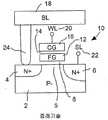
도 1a-1d는 종래 기술의 플로팅 게이트 메모리 셀을 도시한다. 플래시 메모리 셀(10)은 p형 기판(2) 내에 형성된다. n+ 드레인 영역(6) 및 n+ 소스 영역(4)은 p형 기판(2) 내에 형성된다.1A-1D illustrate a prior art floating gate memory cell. The
비교적 얇은 게이트 유전체 또는 터널링 옥사이드(8)는 p형 기판(2)의 표면 상에 증착된다. 다결정 실리콘 플로팅 게이트(poly-crystalline floating gate)(12)는 드레인 영역(6) 및 소스 영역(4) 사이의 채널 영역(5) 위의 터널링 옥사이드(8)의 표면 상에 형성된다. 인터폴리 유전체층(interpoly dielectric layer)(14)은 컨트롤 게이트(16)를 형성하는 다결정 실리콘의 두번째 층으로부터 플로팅 게이트(12)를 분리하기 위해 플로팅 게이트(12) 상에 위치한다.A relatively thin gate dielectric or
EEPROM 또는 플래쉬 메모리의 대부분의 어플리케이션에서, p형 기판(2)은, 대부분의 경우에는 접지 기준 포텐셜(0V)인, 전압을 바이어스하는 기판에 접속된다. 소스 영역(4)은 소스 라인 단자(22)를 통해 소스 전압 발생기에 접속된다. 컨트롤 게이트(16)는 워드 라인 단자(word line terminal)(20)를 통해 컨트롤 게이트 전압 발생기에 접속된다. 상기 드레인 영역(6)은 접촉부(24)를 통해 비트 라인, 따 라서 비트 라인 전압 발생기에 접속된다.In most applications of EEPROM or flash memory, the p-
메모리 셀(10)은 STI(shallow trench isolation)(26)에 의해 기판 상의 집적 회로의 회로 또는 인접한 메모리 셀로부터 분리된다. STI(26)는 인접한 셀의 임의의 작동으로부터의 방해 신호(disturbing signal)로부터 레벨 절연을 제공한다.
공지된 바와 같이, 컨트롤 게이트(16) 및 플로팅 게이트(12)의 결합률(coupling ratio)은 플로팅 게이트(12)로부터 또는 게이트로 전하의 흐름을 야기하기 위해 터널링 옥사이드(8)에 걸쳐 인가되는 전압의 크기를 결정하는데 결정적이다. 따라서 플로팅 게이트(12)에 대해 비교적 큰 결합률을 유지하는 것이 바람직하다. 이를 달성하기 위해, 상기 플로팅 게이트는 통상적으로 "윙(wing)"(28)이라고 칭해지는 것을 형성하기 위해 STI(26) 위로 연장된다. 상기 "윙"(28)은 컨트롤 게이트(16)에 걸쳐 인가되는 전압이 비교적 더 낮도록 하고 계속 전하가 플로팅 게이트(12)로 또는 게이트로부터 흐르도록 한다. 그러나, 상기 "윙"은 최소 크기를 달성하고자 하는 메모리 셀(10)의 설계를 방해한다.As is known, the coupling ratio of the
종래의 작동에 따르면, 상기 메모리 셀(10)은 워드 라인(20)을 통해 컨트롤 게이트(16)로 (10V와 비슷한) 비교적 높은 전압을 인가함으로써 프로그램된다. 드레인 전압 발생기(VD)는 (5V와 유사한) 적당히 높은 전압에 설정되고, 반면 소스 전압 발생기(VS)는 접지 기준 포텐셜(0V)에 설정된다. 상기 전압으로 열전자(hot electron)가 드레인 영역(6) 근처 채널(5)에서 생성될 것이다. 상기 열전자는 터널링 옥사이드(8)를 가로질러 가속되기 충분한 에너지를 갖을 것이고 플로팅 게이트(12) 상에서 트랩(trap)된다. 상기 트랩된 열전자는 메모리 셀(10)에 의해 형성되 는 FET(field effect transistor)의 임계 전압이 3 내지 5 볼트 만큼 증가되도록 할 것이다. 상기 트랩된 열전자에 의한 임계 전압 상의 상기 변화는 셀이 논리 1의 프로그램되지 않은 상태로부터 논리 0으로 프로그램되도록 한다.According to conventional operation, the
종래에, 메모리 셀은 워드 라인(20)을 -18V와 비슷한 비교적 큰 음의 전압으로 설정함으로써 소거된다. 비트 라인(18) 및 소스 라인(22)은 드레인(6) 및 소스(4)가 부유하도록 접속이 해제될 수 있다. 대안으로, 비트 라인(18) 및 소스 라인(22)이 접속되어 드레인(6) 및 소스(4)가 접지 기준 전압에 접속되도록 한다. 이러한 조건들하에서는 채널 영역(5)에서 터널링 옥사이드(8)에 걸쳐 전개되는 큰 전기장이 존재한다. 상기 장은 플로팅 게이트(12) 내에 트랩된 전자들이 채널 영역(5), 드레인 영역(6), 및 소스 영역(4)으로 흐르도록 한다. 다음으로 전자들은 Fowler-Nordheim 터널링에 의해 플로팅 게이트(12)로부터 빠져나오게 된다. 상기 트랩된 열전자의 제거에 의한 임계 전압의 변화는 셀이 소거된 (프로그램되지 않은) 상태가 되게 한다.Conventionally, memory cells are erased by setting
메모리 셀이 논리 1로 쓰여진다면, 상기 셀은 프로그램되지 않고 음의 전하는 플로팅 게이트(12) 상에 전혀 또는 거의 위치되지 않는다. 따라서, 셀이 소거되면, 워드 라인(20)을 통해 컨트롤 게이트(16)에 인가되는 비교적 큰 음의 전압은 메모리 셀(10)이 과소거(over-erased)되도록 한다. 양의 전하는 사실상 플로팅 게이트(12) 상에 저장된다. 이러한 현상은 메모리 셀(10)의 FET가 공핍-모드 트랜지스터(depletion-mode transistor)가 되고 드레인(6) 및 소스(4)가 본질적으로 단축되게 한다. 이러한 현상이 발생되면, 메모리 셀(10)은 과소거된 메모리 셀을 갖는 어레이의 공유된 비트 라인 상의 선택된 메모리 셀로부터 데이터를 잘못 판독(false reading) 하게 한다. 이러한 문제점을 극복하기 위해, 도 2a-2c에 도시된 바와 같이, 선택 게이팅 트랜지스터(select gating transistor: STx)(30)가 메모리 셀(10) 및 소스 라인(22) 사이에 배치된다. 이는 상기 선택 게이팅 트랜지스터(30)가 off 상태로 남아있을 때 메모리 셀(10)을 통해 임의의 초과 전류가 흐르는 것을 막는다.If the memory cell is written to
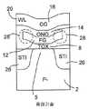
도 2a-2c는 종래 기술의 두개의 트랜지스터 메모리 셀의 추가 논의를 위한 도면이다. 상기 메모리 셀(10)은 p형 기판(2) 상의 n형 웰(n-type well)(34)에 형성된 p형 웰(36) 내에 형성된다. n+ 드레인 영역(6) 및 n+ 소스 영역(4)은 p형 웰(36) 내에 형성된다.2A-2C are diagrams for further discussion of two transistor memory cells of the prior art. The
비교적 얇은 터널링 옥사이드(8)는 p형 기판(2)의 표면 상에 증착된다. 다결정 실리콘 플로팅 게이트(poly-crystalline floating gate)(12)는 드레인 영역(6) 및 소스 영역(4) 사이의 채널 영역(5) 위의 터널링 옥사이드(8)의 표면 상에 형성된다. 인터폴리 유전체층(interpoly dielectric layer)(14)은 컨트롤 게이트(16)를 형성하는 다결정 실리콘의 두번째 층으로부터 플로팅 게이트(12)를 분리하기 위해 플로팅 게이트(12) 상에 위치한다.Relatively
소스 영역(4)은 기본적으로 선택 게이팅 트랜지스터(30)의 드레인이다. 선택 게이팅 트랜지스터(30)의 소스 영역(38)은 메모리 셀(10)의 소스 영역(4) 및 드레인 영역(6)과 동시에 형성된다. 선택 게이팅 트랜지스터(30)의 게이트(40)는 메모리 셀(10)의 소스 영역(4)과 선택 게이팅 트랜지스터(30)의 소스 영역(38) 사이의 게이트 옥사이드(39) 위에 배치된다.
터널링 옥사이드(8)가 형성될 때, 게이트 옥사이드(39)는 메모리 셀(10)의 소스 영역(4)과 선택 게이팅 트랜지스터(30)의 소스 영역(38) 사이의 채널 영역에 형성된다. 게이트(40)는 메모리 셀의 과소거의 임펙트를 제어하기 위해 선택 신호를 선택 게이팅 트랜지스터(30)에 전달하는 선택 컨트롤 라인(SG)에 접속된다.When tunneling
두개의 트랜지스터 구성을 갖는 EEPROM 또는 플래쉬 메모리의, 대부분의 어플리케이션에서, p형 웰(36)은 대부분의 경우 접지 기준 포텐셜(0V)인, 전압을 바이어스하는 기판에 접속된다. 선택 게이팅 트랜지스터(30)의 소스 영역(38)은 소스 라인 단자(22)를 통해 소스 전압 발생기에 접속된다. 컨트롤 게이트(16)는 워드 라인 단자(20)를 통해 컨트롤 게이트 전압 발생기에 접속된다. 선택 게이트 라인(32)은 선택 게이팅 트랜지스터(30)의 게이트(40)에 선택 신호를 제공하기 위해 선택 신호 발생기에 접속된다. 드레인 영역(6)은 접촉부(24)를 통해 비트 라인(18), 비트 라인 전압 발생기에 접속된다.In most applications, in an EEPROM or flash memory having a two transistor configuration, the p-
메모리 셀(10) 및 선택 게이팅 트랜지스터는 STI(26)에 의해 기판 상의 집적 회로의 회로 또는 인접한 메모리 셀로부터 분리된다. 상기 STI(26)는 인접한 셀의 임의의 작동으로부터의 방해 신호로부터 레벨 절연을 제공한다.The
공지의 전술된 바와 같이, 플로팅 게이트는 "윙"(28)을 형성하기 위해 STI(26) 위로 연장된다. "윙"(28)은 컨트롤 게이트(16)에 걸쳐 인가된 전압이 비교적 더 낮아지도록 하고 계속 전하가 플로팅 게이트(12)로 또는 게이트로부터 흐르도록 한다. 그러나, "윙"은 최소 크기를 달성하고자 하는 메모리 셀(10)의 설계를 방해 한다.As noted above, the floating gate extends over the
메모리 셀(10)은 메모리 셀(10)의 드레인 영역(6)을 +15V 이상의 전압으로 설정함으로써 프로그램된다. 컨트롤 게이트(16)는 접지 기준 전압 레벨에서 설정되고 소스 영역(4)은 전류 누설을 피하기 위해 소스 라인을 접속 해제함으로써 부유하도록 구성된다. 드레인 영역(6) 및 채널(5)의 상기 +15V 전압은 비트 라인(18)으로부터 결합된다. 선택 게이트 라인(32)을 통한 게이트(40)는 접지 기준 전압에 설정된다. 이는 드레인 영역(6)의 높은 전압을 일으키고 채널(5)은 플로팅 게이트(12)로부터 드레인 영역(6)으로 전하의 Fowler-Nordheim 터널링을 일으킨다.The
종래에, 메모리 셀은 워드 라인을 설정함으로써 소거되고 따라서 컨트롤 게이트(16)는 대략 +15.0V 내지 +17.0V에서 바이어스된다. 비트 라인(18)을 통한 드레인 영역(6) 및 선택 게이팅 트랜지스터(30)와 소스 라인(22)을 통한 소스 영역(4)은 모두 접지 기준 전압 레벨에서 유지된다. 선택 게이팅 트랜지스터(30)의 게이트(40)는 +3.0V 내지 +5V 의 전압에서 배치되고 비트 라인(18)은 드레인 영역(6)이 접지 기준 전압에 설정되는 것이 보장되도록 접지 기준 전압에서 배치된다.Conventionally, memory cells are erased by setting word lines so
종래의 공지된 메모리 셀의 다른 구성은 컨트롤 게이트와 플로팅 게이트가 타이트하게 결합되는 영역의 증가를 통해 결합 계수(coupling coefficient)를 증가한다. 다른 구성은 선택 게이팅 트랜지스터 및 메모리 셀을 셀 크기를 개선하도록 효과적으로 병합한다. 또한 다른 구성은 비트 라인 및 소스 라인에 접속된 셀 상의 작동으로부터 교란(disturbance)을 방지하기 위해 메모리 셀을 비트 라인 뿐만 아니라 소스 라인으로부터 절연하는 더 많은 게이팅 트랜지스터를 제공한다.Another configuration of a conventionally known memory cell increases the coupling coefficient through an increase in the area where the control gate and the floating gate are tightly coupled. Another configuration effectively merges select gating transistors and memory cells to improve cell size. Other configurations also provide more gating transistors to isolate memory cells from the source lines as well as the bit lines to prevent disturbances from operations on cells connected to the bit lines and source lines.
미국 특허 6,370,081(Sakui 등)은 메모리 셀 및 메모리 셀 사이의 두개의 선택 트랜지스터를 구비한 비휘발성 메모리 셀을 개시한다. 비휘발성 메모리 셀의 한 블록은 하나의 컨트롤 게이트 라인을 구비한다. 비휘발성 메모리 셀은 하나의 페이지를 형성하기 위해 하나의 컨트롤 게이트 라인에 접속된다. 래치 기능(latch function)을 갖는 감지 증폭기는 비트 라인에 접속된다. 데이터 변경 작동에서, 한 페이지의 메모리 셀의 데이터는 감지 증폭기로 판독된다. 데이터가 감지되고 감지 증폭기에 저장된 후 페이지 소거가 수행된다. 감지 증폭기로부터의 데이터는 한 페이지의 메모리 셀에서 프로그램된다. 감지 증폭기에서의 데이터는 바이트 또는 페이지 데이터 프로그래밍을 허용하기 위해 재프로그램되기 전에 감지 증폭기에서 변경될 수 있다.US Patent 6,370,081 (Sakui et al.) Discloses a nonvolatile memory cell having two select transistors between a memory cell and a memory cell. One block of nonvolatile memory cells has one control gate line. The nonvolatile memory cell is connected to one control gate line to form one page. A sense amplifier with a latch function is connected to the bit line. In the data change operation, the data of one page of memory cells is read into the sense amplifier. After data is sensed and stored in the sense amplifier, page erase is performed. Data from the sense amplifier is programmed in one page of memory cells. The data in the sense amplifier can be changed in the sense amplifier before being reprogrammed to allow byte or page data programming.
미국 특허 6,400,604(Noda)는 데이터 재프로그램 모드를 갖는 비휘발성 반도체 메모리 소자를 개시한다. 상기 메모리는 메모리 셀 어레이, 페이지 어드레스 신호에 따라 선택되는, 메모리 셀로 프로그램될 한 페이지 데이터를 저장하는 페이지 버퍼를 구비한다. 상기 메모리는 또한 페이지 버퍼에 저장되는 하나의 데이터를 메모리 셀로 전송하기 위해 페이지 어드레스 신호를 입력하여 하나의 페이지의 컬럼 어드레스를 발생하는 내부 컬럼 어드레스 발생 회로, 상기 내부 컬럼 어드레스 발생 회로로부터 컬럼 어드레스를 수신하는 컬럼 디코더, 및 데이터 재프로그램 모드를 구비하는 컨트롤 회로를 구비한다. 상기 데이터 재프로그램 모드는 페이지 어드레스 신호에 따라 선택된 메모리 셀에 저장된 한 페이지 데이터를 소거하고 선택된 메모리 셀로 페이지 버퍼에 저장된 한 페이지 데이터를 프로그램한다.No. 6,400,604 (Noda) discloses a nonvolatile semiconductor memory device having a data reprogramming mode. The memory has a memory cell array, a page buffer for storing one page data to be programmed into the memory cell, selected according to the page address signal. The memory also receives an internal column address generating circuit for generating a column address of one page by inputting a page address signal to transfer one data stored in the page buffer to the memory cell, and receiving the column address from the internal column address generating circuit. And a control circuit having a column decoder and a data reprogram mode. The data reprogram mode erases one page data stored in the selected memory cell according to the page address signal and programs one page data stored in the page buffer into the selected memory cell.
미국 특허 6,307,781(Shum)은 2 트랜지스터 셀 노어형 아키텍쳐 플래쉬 메모리(NOR architecture flash memory)를 제공한다. 플로팅 게이팅 트랜지스터는 선택 트랜지스터와 관련된 비트 라인 사이에 배치된다. 상기 플래쉬 메모리는 트리플 웰(triple well) 내에 증착되고 Fowler-Nordheim 터널 메카니즘에 따라 작동한다. 메모리 셀의 프로그래밍은 드레인 또는 소스 영역으로부터 플로팅 게이트로의 터널링보다 채널 영역으로부터 플로팅 게이트로 게이트 옥사이드를 통해 캐리어의 터널링을 포함한다.US Patent 6,307,781 (Shum) provides a two transistor cell NOR architecture flash memory. The floating gating transistor is disposed between the bit lines associated with the select transistor. The flash memory is deposited in a triple well and operates according to the Fowler-Nordheim tunnel mechanism. Programming of the memory cell involves tunneling of the carrier through the gate oxide from the channel region to the floating gate rather than tunneling from the drain or source region to the floating gate.
미국 특허 6,212,102(Georgakos 등)는 소스측 선택부를 갖는 2 트랜지스터 메모리 셀을 구비한 EEPROM을 도시한다. 메모리 셀을 프로그램하는데 요구되는 전압은 소스 라인을 통해 전달된다.US Patent 6,212,102 (Georgakos et al.) Shows an EEPROM having a two transistor memory cell with a source side selector. The voltage required to program the memory cell is transferred through the source line.
미국 특허 6,266,274(Pockrandt 등)은 N-채널 선택 트랜지스터 및 N-채널 메모리 트랜지스터를 구비한 비휘발성의 2 트랜지스터 메모리 셀을 고려한다. 상기 셀에 대한 드라이브 회로는 P-채널 전송 트랜지스터를 포함한다. 전송 채널은 메모리 셀에 앞서는 행 라인(row line)에 접속된다.U.S. Patent 6,266,274 (Pockrandt et al.) Considers a non-volatile two transistor memory cell with an N-channel select transistor and an N-channel memory transistor. The drive circuit for the cell includes a P-channel transfer transistor. The transport channel is connected to a row line preceding the memory cell.
미국 특허 6,174,759(Verhaar 등)는 도 2a-2c에서 설명된 것과 유사한 선택 트랜지스터로서 그러한 고-전압 트랜지스터가 제공된 EEPROM 셀을 개시한다. n-웰 주입과 별도로, p-채널의 고-전압 트랜지스터가 논리로 P-채널 트랜지스터와 동일한 프로세스 단계에 의해 주로 제조되어, 프로세스 단계의 수가 여전히 제한적이다.US Patent 6,174,759 (Verhaar et al.) Discloses an EEPROM cell provided with such a high-voltage transistor as a select transistor similar to that described in FIGS. 2A-2C. Apart from n-well implantation, p-channel high-voltage transistors are mainly manufactured by the same process steps as P-channel transistors in logic, so the number of process steps is still limited.
미국 특허 6,326,661(Dormans 등)은 컨트롤 게이트와 플로팅 게이트 사이에 대형 정전 결합(capacitive coupling)을 갖는 플로팅 게이트 메모리 셀을 개시한다. 컨트롤 게이트는 플로팅 게이트의 실질적으로 평평한 표면부와 적어도 소스 및 드레인과 대향하는 플로팅 게이트의 측벽부(side-wall portion)에 정전적으로 결합되고, 선택 게이트의 실질적으로 평평한 표면부 위에서 종단된다. 이는 메모리 셀의 컨트롤 게이트 및 플로팅 게이트 사이의 대형 정전 결합을 갖는 반도체 소자를 제공한다.US Patent 6,326,661 (Dormans et al.) Discloses a floating gate memory cell having a large capacitive coupling between the control gate and the floating gate. The control gate is electrostatically coupled to a substantially flat surface portion of the floating gate and at least a side-wall portion of the floating gate opposite the source and drain, and terminates above the substantially flat surface portion of the selection gate. This provides a semiconductor device having a large electrostatic coupling between the control gate and the floating gate of the memory cell.
본 발명의 동일 양수인에게 양도된, 미국 특허 5,748,538(Lee 등)은 비트-기반의 쓰기 가능성(bit-based write capability)을 갖는 플래시 메모리에 대한 OR-평면 메모리 셀 어레이를 설명한다. 플래쉬 메모리(flash EEPROM) 셀 어레이는 행(row)과 열(column)로 배열된 비휘발성 메모리 셀을 포함한다. 동일한 메모리 블록 내 비휘발성 메모리 셀의 소스는 컨트롤 게이트를 통해 메인 소스 라인에 접속된다. 유사하게, 동일한 메모리 블록의 비휘발성 메모리 셀의 드레인은 메인 비트 라인에 접속된다. 열 방향에서 별개의 소스 및 드레인은 비트-기반의 쓰기 가능성을 갖도록 설계된다. 선택된 비휘발성 메모리 셀의 소거 또는 프로그래밍과 같은, 기록(writing)은 Fowler-Nordheim 터널링 방법을 사용하고 선택되지 않은 비휘발성 메모리 셀에 인가된 프로그래밍 또는 소거 금지 전압으로 인해 성취될 수 있다.U. S. Patent No. 5,748, 538 (Lee et al.), Assigned to the same assignee of the present invention, describes an OR-plane memory cell array for flash memory having bit-based write capability. A flash EEPROM cell array includes nonvolatile memory cells arranged in rows and columns. Sources of nonvolatile memory cells in the same memory block are connected to the main source line through control gates. Similarly, the drains of nonvolatile memory cells of the same memory block are connected to the main bit line. Separate sources and drains in the column direction are designed to have bit-based writeability. Writing, such as erasing or programming a selected nonvolatile memory cell, may be accomplished using a Fowler-Nordheim tunneling method and due to a programming or erase inhibit voltage applied to an unselected nonvolatile memory cell.
본 발명의 목적은 플래쉬 메모리로서 통합을 위한 단일 트랜지스터 메모리 셀 및 EEPROM으로서 통합을 위한 2 트랜지스터 메모리 셀을 갖는 비휘발성 메모리 어레이를 제공하는 것이다.It is an object of the present invention to provide a non-volatile memory array having a single transistor memory cell for integration as flash memory and a two transistor memory cell for integration as EEPROM.
본 발명의 또다른 목적은 소형 메모리 셀을 허용하는 낮은 결합 계수를 갖는 플로팅 게이트를 구비한 단일 트랜지스터 플래쉬 비휘발성 메모리 셀을 제공하는 것이다.It is another object of the present invention to provide a single transistor flash nonvolatile memory cell having a floating gate with a low coupling coefficient that allows a small memory cell.
본 발명의 또다른 목적은 소형 메모리 셀을 허용하는 소형 선택 트랜지스터와 직렬로 접속된 낮은 결합 계수를 갖는 플로팅 게이트를 구비한 2 트랜지스터 EEPROM 비휘발성 메모리 셀을 제공하는 것이다.It is another object of the present invention to provide a two transistor EEPROM nonvolatile memory cell having a floating gate having a low coupling coefficient connected in series with a small select transistor allowing a small memory cell.
본 발명의 또다른 목적은 플래쉬 메모리 및 EEPROM 메모리 셀이 동일한 프로세스 기술을 사용하여 동일한 기판 상에서 통합될 수 있는 메모리 어레이를 제공하는 것이다.It is another object of the present invention to provide a memory array in which flash memory and EEPROM memory cells can be integrated on the same substrate using the same process technology.
상기 및 다른 목적을 달성하기 위해, 비휘발성 메모리 어레이가 기판 상에 형성된다. 비휘발성 메모리 어레이는 행 및 열로 배열된 비휘발성 메모리 셀을 갖는다. 각각의 비휘발성 메모리 셀은 기판의 표면 내에 위치한 소스 영역 및 드레인 영역을 갖는다. 드레인 영역은 기판 내에 채널 영역을 형성하기 위해 소스 영역으로부터 거리를 갖고 위치된다. 터널링 절연층은 소스 영역 및 드레인 영역 사이의 채널 영역의 표면 상에 배치된다. 터널링 절연층 위에 배치된 플로팅 게이트는 소스 영역의 에지 및 드레인 영역의 에지와 정렬되고 소스의 에지 및 드레인의 에지 폭에 의해 지정되는 폭을 갖는다. 컨트롤 게이트는 플로팅 게이트 위에 배치되고 층간 절연체에 의해 플로팅 게이트로부터 절연된다. 플로팅 게이트 및 컨트롤 게이트는 비휘발성 메모리 셀의 스켈링을 허용하도록 링 없이 50% 이하의 비교적 작은 결합률을 갖는다.In order to achieve the above and other objects, a nonvolatile memory array is formed on a substrate. Nonvolatile memory arrays have nonvolatile memory cells arranged in rows and columns. Each nonvolatile memory cell has a source region and a drain region located within the surface of the substrate. The drain region is positioned at a distance from the source region to form a channel region in the substrate. The tunneling insulating layer is disposed on the surface of the channel region between the source region and the drain region. The floating gate disposed over the tunneling insulating layer has a width that is aligned with the edge of the source region and the edge of the drain region and is specified by the edge width of the edge of the source and the drain. The control gate is disposed above the floating gate and insulated from the floating gate by an interlayer insulator. The floating gate and control gate have a relatively small coupling rate of 50% or less without a ring to allow scaling of nonvolatile memory cells.
비휘발성 메모리의 각 열은 비휘발성 메모리 셀의 열 상의 모든 비휘발성 메모리 셀의 드레인 영역과 교통하는 비트 라인을 가진다. 유사하게, 비휘발성 메모리 셀의 각 행은 비휘발성 메모리 셀의 행의 모든 비휘발성 메모리 셀의 소스 영역에 접속된 소스 라인을 갖는다. 비휘발성 메모리 어레이는 비휘발성 메모리 셀의 각 행의 모든 비휘발성 메모리 셀의 컨트롤 게이트에 접속된 워드 라인을 갖는다.Each column of nonvolatile memory has a bit line in communication with the drain region of all nonvolatile memory cells on the column of nonvolatile memory cells. Similarly, each row of nonvolatile memory cells has a source line connected to the source region of all nonvolatile memory cells of the row of nonvolatile memory cells. The nonvolatile memory array has word lines connected to the control gates of all nonvolatile memory cells of each row of nonvolatile memory cells.
비휘발성 메모리 어레이가 단일 트랜지스터 비휘발성 메모리 셀을 갖는 경우에는, 선택된 비휘발성 메모리 셀은 선택된 비휘발성 메모리 셀의 컨트롤 게이트에 접속된 워드 라인에 대략 +10.0V 내지 대략 +12.0V의 적절히 높은 양의 전압을 먼저 인가함으로써 선택된 비휘발성 메모리 셀의 플로팅 게이트 위에 전하를 위치시켜 프로그램된다. 대략 5.0V의 중간의 양의 전압이 선택된 비휘발성 메모리 셀의 드레인 영역과 교통하는 비트 라인에 인가되어 중간의 양의 전압이 드레인 영역으로 전달되고 접지 기준 전압이 선택된 비휘발성 메모리 셀의 소스에 접속된 소스 라인에 인가된다.If the nonvolatile memory array has a single transistor nonvolatile memory cell, the selected nonvolatile memory cell may contain an appropriately high amount of approximately + 10.0V to approximately + 12.0V at a word line connected to the control gate of the selected nonvolatile memory cell. It is programmed by placing a charge on the floating gate of the selected nonvolatile memory cell by first applying a voltage. A medium positive voltage of approximately 5.0 V is applied to the bit line in communication with the drain region of the selected nonvolatile memory cell such that an intermediate positive voltage is transferred to the drain region and a ground reference voltage is connected to the source of the selected nonvolatile memory cell. Is applied to the source line.
적절히 높은 양의 게이트 전압, 중간의 양의 드레인 전압을 인가하고, 접지 기준 소스 전압을 인가하는 단일 트랜지스터 플래쉬 메모리 셀에 대한 프로그램 시간의 지속 시간은 대략 1㎲ 내지 대략 100㎲이다.The duration of program time for a single transistor flash memory cell applying a moderately high gate voltage, a medium positive drain voltage, and a ground reference source voltage is approximately 1 ms to approximately 100 ms.
단일 트랜지스터를 갖는 선택된 메모리 셀은 선택된 메모리 셀의 컨트롤 게이트에 접속된 워드 라인에 대략 -15V 내지 대략 -22V의 매우 큰 음의 전압을 인가함으로써 플로팅 게이트로부터 전기 음전하를 제거하여 소거된다.The selected memory cell with a single transistor is erased by removing the electrical negative charge from the floating gate by applying a very large negative voltage of approximately -15V to approximately -22V to the word line connected to the control gate of the selected memory cell.
선택된 메모리 셀의 소스 영역에 접속된 소스 라인 및 선택된 비휘발성 메모리 셀의 드레인 영역과 교통하는 비트 라인은 접속 해제되어 소스 영역 및 드레인 영역을 부유하게 한다. 대안으로, 선택된 비휘발성 메모리 셀의 소거 동안 접지 기준 전압이 선택된 메모리 셀의 소스 영역에 접속된 소스 라인 및 선택된 비휘발성 메모리 셀의 드레인 영역과 교통하는 비트 라인에 인가된다. 비휘발성 메모리 셀의 소거는 1ms 내지 대략 1s의 지속 시간을 갖는다.The source line connected to the source region of the selected memory cell and the bit line communicating with the drain region of the selected nonvolatile memory cell are disconnected to float the source region and the drain region. Alternatively, a ground reference voltage is applied to the source line connected to the source region of the selected memory cell and the bit line in communication with the drain region of the selected nonvolatile memory cell during erase of the selected nonvolatile memory cell. Erasing the nonvolatile memory cell has a duration of 1 ms to approximately 1 s.
비휘발성의 단일 트랜지스터 플래쉬 메모리 어레이는 분리된 비트 라인 어레이 아키텍쳐에 대한 게이팅 트랜지스터를 갖는 비휘발성 메모리 셀을 구비한다. 게이팅 트랜지스터는 제1 금속에 의해 플로팅 게이트를 갖는 트랜지스터의 드레인 영역에 접속된 소스를 구비한다. 게이팅 트랜지스터는 제2 금속에 의해 구형의 비트 라인에 접속된 드레인 및 비트 라인 전압 신호를 드레인 영역에 선택적으로 인가하기 위해 선택 게이트 신호를 수신하도록 선택 라인에 접속된 게이트를 또한 구비한다. 또한 비휘발성 메모리 어레이는 게이팅 선택 라인을 구비한다. 각각의 게이팅 선택 라인은 비휘발성 메모리 셀의 하나의 행의 비휘발성 메모리 셀 각각의 게이팅 트랜지스터의 게이트에 접속된다.Non-volatile single transistor flash memory arrays include non-volatile memory cells with gating transistors for separate bit line array architectures. The gating transistor has a source connected by a first metal to a drain region of the transistor having a floating gate. The gating transistor also has a gate connected to the select line to receive the select gate signal for selectively applying a drain and bit line voltage signal connected to the spherical bit line by the second metal to the drain region. The nonvolatile memory array also has a gating select line. Each gating select line is connected to the gate of a gating transistor of each of the nonvolatile memory cells of one row of nonvolatile memory cells.
비휘발성 메모리 셀의 플로팅 게이트 위에 전하를 배치하는 프로그래밍은 선택된 비휘발성 메모리 셀의 컨트롤 게이트에 접속된 워드 라인에 대략 +10.0V 내지 대략 +12.0V의 적절히 높은 양의 전압을 인가함으로써 시작한다. 대략 6.0V의 중간의 양의 전압은 선택된 비휘발성 메모리 셀의 드레인 영역 게이팅 트랜지스터에 접속된 구형의 비트 라인에 인가되어 5V의 중간의 양의 전압이 플로팅 게이트를 갖는 트랜지스터의 드레인 영역에 전달된다. 접지 기준 전압은 선택된 비휘발성 메모리 셀의 플로팅 게이트를 갖는 트랜지스터의 소스에 접속된 소스 라인에 인가된다. 매우 큰 양의 전압은 선택된 비휘발성 메모리 셀의 게이팅 트랜지스터의 게이트에 접속된 선택 라인에 인가된다.Programming to place charge over the floating gate of a nonvolatile memory cell begins by applying a moderately high positive voltage of approximately + 10.0V to approximately + 12.0V to a word line connected to the control gate of the selected nonvolatile memory cell. A positive positive voltage of approximately 6.0V is applied to a spherical bit line connected to the drain region gating transistor of the selected nonvolatile memory cell so that a positive positive voltage of 5V is transferred to the drain region of the transistor having the floating gate. The ground reference voltage is applied to a source line connected to the source of the transistor having the floating gate of the selected nonvolatile memory cell. A very large amount of voltage is applied to the select line connected to the gate of the gating transistor of the selected nonvolatile memory cell.
선택된 비휘발성 메모리 셀을 프로그램하기 위해 매우 큰 양의 선택 게이트 전압, 적절히 높은 양의 컨트롤 게이트 전압, 중간의 양의 비트 라인 전압을 인가하고, 접지 기준 전압을 인가하는 지속 시간은 대략 1㎲ 내지 대략 100㎲이다.The duration of applying a very large amount of select gate voltage, a moderately high amount of control gate voltage, a medium amount of bit line voltage, and a ground reference voltage for programming the selected non-volatile memory cell is approximately 1 s to approximately 100 ㎲.
선택된 비휘발성 메모리 셀의 플로팅 게이트로부터 전기 음전하를 제거하는 소거는 선택된 비휘발성 메모리 셀의 게이팅 트랜지스터의 컨트롤 게이트에 접속된 워드 라인에 대략 -15V 내지 대략 -22V의 매우 큰 음의 전압을 인가함으로써 시작한다. 선택 신호는 접지 기준 전압으로 설정되고 선택된 비휘발성 메모리 셀의 게이팅 트랜지스터의 게이트에 접속된 선택 라인에 인가된다. 소스 라인은 선택된 비휘발성 메모리 셀의 플로팅 게이트를 갖는 트랜지스터의 소스 영역에 접속되고 비트 라인은 선택된 비휘발성 메모리 셀의 게이팅 트랜지스터의 드레인에 접속된다.Erasing, which removes the electrical negative charge from the floating gate of the selected nonvolatile memory cell, begins by applying a very large negative voltage of approximately -15V to approximately -22V to a word line connected to the control gate of the gating transistor of the selected nonvolatile memory cell. do. The select signal is set to the ground reference voltage and applied to the select line connected to the gate of the gating transistor of the selected nonvolatile memory cell. The source line is connected to the source region of the transistor having the floating gate of the selected nonvolatile memory cell and the bit line is connected to the drain of the gating transistor of the selected nonvolatile memory cell.
대안으로, 선택된 비휘발성 메모리 셀의 플로팅 게이트를 갖는 트랜지스터의 소스 영역에 접속된 소스 라인 및 선택된 비휘발성 메모리 셀의 게이팅 트랜지스터의 드레인에 접속된 비트 라인에 접지 기준 전압이 인가된다. 메모리 셀의 소거 지속 시간은 대략 1ms 내지 대략 1s이다.Alternatively, a ground reference voltage is applied to the source line connected to the source region of the transistor having the floating gate of the selected nonvolatile memory cell and the bit line connected to the drain of the gating transistor of the selected nonvolatile memory cell. The erase duration of the memory cell is approximately 1 ms to approximately 1 s.
도 1a-1d는 종래 기술의 단일 트랜지스터 비휘발성 플로팅 게이트 메모리 셀의 다이어그램이자 단면도이다.1A-1D are diagrams and cross-sectional views of prior art single transistor nonvolatile floating gate memory cells.
도 2a-2c는 종래 기술의 2 트랜지스터 비휘발성 플로팅 게이트 메모리 셀의 다이어그램이자 단면도이다.2A-2C are diagrams and cross-sectional views of a two transistor nonvolatile floating gate memory cell of the prior art.
도 3a-3d는 본 발명의 단일 트랜지스터 비휘발성 플로팅 게이트 메모리 셀의 다이어그램이자 단면도이다.3A-3D are diagrams and cross-sectional views of a single transistor nonvolatile floating gate memory cell of the present invention.
도 4는 본 발명의 단일 트랜지스터 비휘발성 메모리 셀의 어레이의 개략도이다.4 is a schematic diagram of an array of single transistor nonvolatile memory cells of the present invention.
도 5a-5c는 본 발명의 2 트랜지스터 비휘발성 플로팅 게이트 메모리 셀의 다이어그램이자 단면도이다.5A-5C are diagrams and cross-sectional views of a two transistor nonvolatile floating gate memory cell of the present invention.
도 6은 본 발명의 2 트랜지스터 비휘발성 메모리 셀의 어레이의 개략도이다.6 is a schematic diagram of an array of two transistor nonvolatile memory cells of the present invention.
도 7은 본 발명의 2 트랜지스터 비휘발성 메모리 셀의 선택 게이팅 트랜지스터에 대한 선택 게이팅 신호 전압 대 채널 폭의 플롯이다.7 is a plot of select gating signal voltage versus channel width for select gating transistors of a two transistor non-volatile memory cell of the present invention.
도 8a는 본 발명의 플래쉬 메모리 비휘발성 메모리 셀을 프로그램하고 소거하는 전압 레벨을 약술하는 표이다.8A is a table outlining the voltage levels for programming and erasing flash memory non-volatile memory cells of the present invention.
도 8b는 본 발명의 EEPROM 비휘발성 메모리 셀을 프로그램하고 소거하는 전압 레벨을 약술하는 표이다.8B is a table outlining the voltage levels for programming and erasing the EEPROM nonvolatile memory cells of the present invention.
도 9a 및 도 9b는 프로그래밍 및 소거를 위한 본 발명의 비휘발성 메모리 셀의 임계 전압의 분포를 도시하는 플롯이다.9A and 9B are plots showing the distribution of threshold voltages of nonvolatile memory cells of the present invention for programming and erasing.
도 10은 본 발명의 비휘발성 메모리 셀에 대한 프로그램 및 소거 작동 지속 기간을 결정하는 본 발명의 비휘발성 메모리 셀에 대한 시간 대 임계 전압의 플롯이다.10 is a plot of time versus threshold voltage for a nonvolatile memory cell of the present invention that determines the duration of program and erase operations for the nonvolatile memory cell of the present invention.
도 11a-11m은 본 발명의 단일 트랜지스터 비휘발성 메모리 셀의 형성을 위한 단계를 도시하는 기판의 단면도이다.11A-11M are cross-sectional views of a substrate showing the steps for forming a single transistor nonvolatile memory cell of the present invention.
도 12a-12c는 본 발명의 2 트랜지스터 비휘발성 메모리 셀의 형성을 위한 추가적인 단계를 도시하는 기판의 단면도이다.12A-12C are cross-sectional views of a substrate showing additional steps for forming a two transistor nonvolatile memory cell of the present invention.
전술된 바와 같이 EEPROM 비휘발성 메모리는 프로그램 코드를 저장하는 플래쉬 메모리의 블록 (페이지 또는 전체 칩) 가변성과 달리 EEPROM의 바이트-변경 특징이 데이터 코드를 저장하기 위해 사용된다는 점에서 플래쉬 메모리와 구별된다. EEPROM은 데이터와 같이 종종 변경되는 정보를 보유하기 위해 사용되기 때문에, EEPROM은 바이트 단위로 프로그램하고 소거하는 사이클에 의존하고, 따라서 EEPROM은 더 높은 내구성을 가져야 한다. 백만 사이클의 높은 내구성을 달성하기 위해, 선택되지 않은 바이트에 대한 고전압 비트라인 (프로그램) 및 워드라인 (소거) 디스터브(disturb)는 프로그램 및 소거 작동을 반복하는 동안 제거되어야 한다. 이는 대형이고 비확장성(non-scalable)이나 전혀 비트라인 프로그램 디스터브를 주지않는 2 트랜지스터 EEPROM 비휘발성 메모리 셀로 이르게 한다. 또한, EEPROM 셀 어레이의 워드라인은 통상적으로 비선택된 바이트에 대한 워드라인 소거 디스터브를 회피하기 위해 분할되었다. 대안으로, 플래쉬 메모리는 소형의 셀을 갖으나 블록 단위로 더 긴 프로그램 및 소거 시간을 요구하는 단일 트랜지스터 비휘발성 메모리 셀이다. 셀의 셀 크기를 줄이고 단일화된 플래쉬 메모리 및 EEPROM 설계를 제공하기 위해, 본 발명은 어떠한 오버랩 없이 소스 영역 및 드레인 영역의 에지 사이에 배치되고 에지와 정렬되는 플로팅 게이트를 갖는 비휘발성 메모리 셀 내 트랜지스터를 제공한다. 또한, 도 1a-1d 및 2a-2c에 도시된 바와 같은 "윙"이 컨트롤 게이트 및 플로팅 게이트의 결합 계수를 줄이기 위해 제거된다. 상기 감소된 결합 계수는 프로그램 및 소거 작동의 동일한 효과를 유지하기 위해 더 높은 컨트롤 게이트 전압을 요구한다.As described above, EEPROM nonvolatile memory is distinguished from flash memory in that the byte-change feature of the EEPROM is used to store data code, unlike block (page or entire chip) variability of flash memory that stores program code. Since EEPROMs are used to hold information that often changes, such as data, EEPROMs rely on cycles of programming and erasing byte by byte, so EEPROMs must have higher durability. To achieve high endurance of one million cycles, the high voltage bitline (program) and wordline (erase) disturbances for the unselected bytes must be removed during repeat program and erase operations. This leads to a two-transistor EEPROM nonvolatile memory cell that is large and non-scalable or without any bitline program disturb. In addition, the wordline of the EEPROM cell array is typically partitioned to avoid wordline erase disturbs for unselected bytes. Alternatively, a flash memory is a single transistor nonvolatile memory cell having a small cell but requiring longer program and erase time on a block basis. In order to reduce the cell size of the cell and provide a unified flash memory and EEPROM design, the present invention provides a transistor in a nonvolatile memory cell having a floating gate disposed between and aligned with the edge of the source and drain regions without any overlap. to provide. Also, "wings" as shown in FIGS. 1A-1D and 2A-2C are removed to reduce the coupling coefficients of the control gate and floating gate. The reduced coupling coefficient requires a higher control gate voltage to maintain the same effect of program and erase operations.
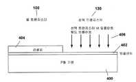
도 3a-3d는 본 발명의 단일 트랜지스터 플로팅 게이트 플래쉬 메모리 셀을 도시한다. 비휘발성 메모리 셀(100)은 p형 기판(102) 내에 형성된다. n+ 드레인 영역(104) 및 n+ 소스 영역(106)은 p형 기판(102) 내에 형성된다.3A-3D illustrate a single transistor floating gate flash memory cell of the present invention. The
비교적 얇은 게이트 유전체 또는 터널링 옥사이드(108)는 p형 기판(102)의 표면 상에 증착된다. 다결정 실리콘 플로팅 게이트(112)는 드레인 영역(104) 및 소스 영역(106) 사이의 채널 영역(105) 위 터널링 옥사이드(108)의 표면 상에 형성된다. 인터폴리 유전체층(114)은 컨트롤 게이트(116)를 형성하는 다결정 실리콘의 두번째 층으로부터 플로팅 게이트(112)를 분리하기 위해 플로팅 게이트(112) 상에 배치된다.A relatively thin gate dielectric or
플로팅 게이트(112)는 채널 영역(105) 위 드레인 영역(104) 및 소스 영역(106)의 에지(110)와 정렬되도록 제한 된다. 또한, 도 1d에 도시된 바와 같은 "윙"(28)이 없고 플로팅 게이트는 드레인 영역(104) 및 소스 영역(106)의 폭(128)으로 제한된다. 결합 계수는 따라서 도 1a-1d의 비휘발성 메모리 셀 이하(< 50%)이다.The floating
플래쉬 메모리 내 본 발명의 단일 트랜지스터 비휘발성 메모리 셀의 어플리케이션에서, 상기 p형 기판(102)은, 대부분의 경우 접지 기준 포텐셜(0V)인, 전압 을 바이어스하는 기판에 접속된다. 소스 영역(106)은 소스 라인 단자(SL)(122)를 통해 소스 전압 발생기에 접속된다. 컨트롤 게이트(116)는 워드 라인 단자(WL)(120)를 통해 컨트롤 게이트 전압 발생기에 접속된다. 드레인 영역(104)은 접촉부(124)를 통해 비트 라인(118)과 비트 라인 전압 발생기에 접속된다.In the application of the single transistor nonvolatile memory cell of the present invention in flash memory, the p-
메모리 셀(100)은 인접한 메모리 셀 또는 STI(shallow trench isolation)(126)에 의해 기판 상의 집적 회로의 회로와 분리된다. STI(126)는 인접한 셀의 임의의 작동으로부터의 방해 신호으로부터 레벨 절연을 제공한다.
컨트롤 게이트(116) 및 플로팅 게이트(112)의 낮은 결합률을 보상하기 위해, 컨트롤 게이트에 인가된 전압의 크기는 플로팅 게이트(112)로 또는 게이트로부터의 전하의 흐름을 야기하도록 동일한 두께의 터널링 옥사이드(108)에 걸친 동일한 터널링 전기장을 유지하기 위해 증가되어야 한다. 본 발명의 단일 트랜지스터 플래쉬 비휘발성 메모리 셀에서, 프로그래밍 및 소거를 위한 전압은 터널 옥사이드를 갖는 EPROM(EPROM with Tunnel Oxide: ETOX) 플래쉬 기술을 사용하는 종래 기술보다 단지 몇 볼트 더 클뿐이다.In order to compensate for the low coupling rates of the
도 8a에서 도시된 본 발명의 비휘발성 메모리 셀의 작동에 따라, 메모리 셀(100)은 워드 라인(WL)(120)을 통해 컨트롤 게이트(116)에 (+10.0V 내지 +12.0V와 비슷한) 비교적 높은 전압을 인가함으로써 프로그램된다. 드레인 전압 발생기는 비트 라인(BL)(118)과 따라서 드레인 영역(104)을 적당히 높은 전압으로 하기 위해 (5V와 비슷한) 적당히 높은 전압으로 설정 되고, 반면 소스 전압 발생기는 소스 라인(SL)(122)과 따라서 소스 영역(106)을 접지 기준 포텐셜(0V)에 설정하기 위해 접 지 기준 포텐셜에 설정된다. 상기의 전압으로 열전자가 드레인 영역(104) 근처의 채널(105)에서 생성될 것이다. 상기 열전자는 터널링 옥사이드(108)을 가로질러 가속되어 플로팅 게이트(112)에 트랩되기 충분한 에너지를 갖을 것이다. 상기 트랩된 열전자는 메모리 셀(100)에 의해 형성되는 전계 효과 트랜지스터(FET)의 임계 전압이 3 내지 5 볼트 만큼 증가되도록 한다. 트랩된 열전자에 의한 임계 전압 상의 변화는 셀이 논리 1의 프로그램되지 않은 상태로부터 논리 0으로 프로그램되게 한다.In accordance with the operation of the nonvolatile memory cell of the present invention shown in FIG. 8A, memory cell 100 (similar to + 10.0V to + 12.0V) is connected to control
본 발명의 단일 트랜지스터 플래쉬 메모리 셀은 워드 라인 발생기와 따라서 워드 라인(WL)(120)을 통한 컨트롤 게이트(116)를 -15.0V 내지 -22.0V, 바람직하게는 -18.0V의 비교적 큰 음의 전압으로 설정함으로써 소거된다. 비트 라인 전압 발생기와 비트 라인(BL)(118) 및 소스 라인 발생기와 소스 라인(SL)(122)은 드레인 영역(104) 및 소스 영역(106)이 부유하도록 접속 해제될 수 있다. 대안으로, 비트라인 전압 발생기와 비트 라인(BL)(118) 및 소스 라인 발생기와 소스 라인(SL)(122)이 접속되어 드레인 영역(104) 및 소스 영역(106)이 접지 기준 전압에 접속된다. 이러한 조건 하에서 채널 영역(105)에 터널링 옥사이드(108)를 걸쳐 전개되는 큰 전기장이 존재한다. 이 전기장은 플로팅 게이트(112)에 트랩된 전자가 Fowler-Nordheim 터널링에 의해 채널 영역(105)에 흐르도록 한다.The single transistor flash memory cell of the present invention provides a relatively large negative voltage between -15.0 V and -22.0 V, preferably -18.0 V, through the word line generator and thus the
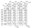
도 4는 플래쉬 메모리 어레이의 블록 내 도 3a-3d의 단일 트랜지스터 플래쉬 비휘발성 메모리 셀의 어플리케이션을 도시한다. 단일 트랜지스터 비휘발성 메모리 셀(100)의 그룹들은 행과 열로 배열된다. 플래쉬 메모리에서, 메모리 셀은 도 3a-3d에 도시된 바와 같이 공통 p형 기판을 갖는 단일 그룹일 수 있다. 그러나, 상기 구조는 트리플-웰 구조로 주로 칭해지는 것에서 처럼 조직될 수 있고, 여기서 대형 n형 웰은 p형 기판 상에 형성되고 소형 p형 웰은 n형 웰 내에 배치된다. 다음으로 비휘발성 메모리 셀(100)의 비교적 큰 블록 또는 서브어레이(200, 205)는 분리된 p형 웰 내에 형성된다. 어레이의 각 행의 각각의 비휘발성 메모리 셀(100)의 컨트롤 게이트는 하나의 워드 라인(225a, ..., 225k)에 접속된다. 유사하게, 어레이의 각 행의 각각의 비휘발성 메모리 셀(100)의 소스는 하나의 소스 라인(230a, ..., 230k)에 접속된다. 어레이의 각 열의 각각의 비휘발성 메모리 셀(100)의 드레인은 제1 금속의 하나의 비트 라인(255a, ..., 225m, 260a, ..., 260m)에 접속된다.4 illustrates an application of the single transistor flash nonvolatile memory cell of FIGS. 3A-3D in a block of a flash memory array. Groups of single transistor
상기 서브어레이는 사실상 수직의 서브어레이(미도시)를 갖을 수 있다. 어레이의 세그먼트 및 어레이의 제어를 추가하기 위해, 각각의 비트 라인(255a,...,225m, 260a,...,260m)은 게이팅 트랜지스터(210a, ..., 210m, 215a, ..., 215m)를 통해 마스터 비트 라인(245a, ..., 245m, 250a, ..., 250m)에 접속된다. 어레이의 각 열의 게이팅 트랜지스터(210a, ..., 210m, 215a, ..., 215m)의 드레인은 제2 금속의 마스터 비트 라인(245a, ..., 245m, 250a, ..., 250m) 중의 하나에 접속된다. 게이팅 트랜지스터(210a, ..., 210m, 215a, ..., 215m)의 각각의 소스는 어레이 열 상의 각각의 비휘발성 메모리 셀(100)의 드레인에 접속된다. 블록(200 또는 205) 또는 다중 블록(200 및 205)에 대한 게이팅 트랜지스터(210a, ..., 210m, 215a, ..., 215m)의 게이트는 선택 게이트 라인(SG)(220)에 접속된다. 각 블록(200 및 205)에 대한 소스 라인(230a, ..., 230k)은 마스터 소스 라인(240a 및 240m) 각각에 개별적으로 접속된다.The subarray may have a substantially vertical subarray (not shown). To add segments of the array and control of the array, each bit line (255a, ..., 225m, 260a, ..., 260m) has a gating transistor (210a, ..., 210m, 215a, ...). 215m are connected to the
다시 도 8a를 참조하면, 선택된 셀의 프로그래밍은 개별적인 셀에 대해 설명된 바와 같다. 프로그램될 셀을 포함하는 워드 라인(225a, ..., 225k) (워드 라인 당 다중 셀이 프로그램될 수 있다)은 (+10.0V 내지 +12.0V와 비슷한) 비교적 높은 전압에서 활성화된다. 게이트 라인(SG)(220) 및 게이팅 트랜지스터(210a, ..., 210m, 215a, ..., 215m)의 게이트는 종래 기술에서 사용되는 약 10V에 대립하여 (+15.0V 내지 +22.0V와 비슷한) 비교적 높은 전압에 설정되어 게이팅 트랜지스터(210a, ..., 210m, 215a, ..., 215m)를 활성화시킨다. 게이트 라인(SG)(220)상의 상기의 매우 높은 전압으로, 트랜지스터(210a, ..., 210m, 215a, ..., 215m)는 실리콘 영역을 줄이기 위해 종래 기술에서의 유사한 장치보다 훨씬 더 소형으로 제조될 수 있다. 선택된 비휘발성 메모리 셀(100)을 포함하는 열의 제2 금속의 마스터 비트 라인(245a,...,245m, 250a,...,250m)은 (5V에 유사한) 적당히 높은 전압으로 설정된다. 마스터 소스 라인(240a,...,240m)은 기준 접지 전압(0V)에 설정된다. 전술된 바와 같이 이는 선택된 비휘발성 메모리 셀(100)의 플로팅 게이트의 채널 열전자가 충전을 일으킨다.Referring again to FIG. 8A, the programming of the selected cell is as described for the individual cell.
프로그램되지 않은 선택된 비휘발성 메모리 셀(상기 셀들은 소거에 의해 논리 1에 설정됨)을 포함하지 않는 마스터 비트 라인(245a,...,245m, 250a,...,250m)은 접지 기준 포텐셜에 설정된다. 게이트 라인(SG)(220)은 매우 높은 전압에 설정되어 프로그램 작동 동안 선택된 비휘발성 메모리 셀을 포함하지 않는 상기 비트 라인(255a, ..., 255m, 260a, ..., 260m)에 대해 게이팅 트랜지스터(210a, ..., 210m, 215a, ..., 215m)를 활성화시킨다. 따라서 선택된 비휘발성 메모리 셀을 포 함하지 않는 비트 라인(255a, ..., 255m, 260a, ..., 260m) 상에 없는 선택되지 않은 메모리 셀의 드레인은 접지 기준 포텐셜(0V)에 설정된다.
선택된 비휘발성 메모리 셀을 포함하는 워드 라인(225a, ..., 225k) 상의 선택되지 않은 메모리 셀은 프로그램 작동 동안 비교적 높은 전압(+10.0V 내지 +12.0V)에 설정된 자체 컨트롤 게이트를 구비한다. 선택되거나 선택되지 않은 블록의 각각의 비휘발성 메모리 셀의 소스는 접지 기준 포텐셜(0V)에 설정된다.Unselected memory cells on
선택된 비휘발성 메모리 셀을 포함하는 비트 라인(255a,...,255m, 260a,...,260m) 상의 선택되지 않은 비휘발성 메모리 셀은 대략 +5V의 비교적 높은 전압에 설정된 자체 드레인을 구비한다. 플로팅 게이트를 구비한 트랜지스터의 게이트 및 소스는 접지 기준 포텐셜(0V)에 설정되기 때문에, 채널 열전자 현상은 발생되지 않고 따라서 선택되지 않은 비휘발성 메모리 셀을 방해하지 않게 한다.Unselected nonvolatile memory cells on
선택된 비휘발성 메모리 셀의 동일한 블록 또는 서브어레이에 있지 않은 그러한 비휘발성 메모리 셀은 서브어레이 내 임의의 방해 신호를 방지하기 위해 자체 게이트 라인(220), 워드 라인(225a, ..., 225k), 비트 라인(255a, ..., 255m, 260a, ..., 260m), 및 소스 라인(230a, ..., 230k)을 구비한다.Such nonvolatile memory cells that are not in the same block or subarray of the selected nonvolatile memory cell may have their
소거는 전체 블록 또는 서브어레이에 대해 발생하고 개별 셀에 대해 설명된 바와 본질적으로 같다. 서브어레이 내 모든 워드 라인(225a, ..., 225k)은 (-15.0V 내지 -22.0V와 비슷한) 비교적 큰 음의 전압에 설정된다. 게이트 라인(SG)(220) 및 게이팅 트랜지스터(210a, ..., 210m, 215a, ..., 215m)의 게이트는 접지 기준 포텐셜(0V)에 설정되어 게이팅 트랜지스터(210a, ..., 210m, 215a, ..., 215m)를 비활 성화한다. 서브어레이의 마스터 비트 라인(245a, ..., 245m, 250a, ..., 250m)은 접지 기준 전압(0V)에 설정된다. 서브어레이의 마스터 소스 라인(240a, ..., 240m) 및 소스 라인(230a, ..., 230k)은 접지 기준 전압(0V)에 설정된다. 전술된 바와 같이 이는 플로팅 게이트로부터 전하의 Fowler-Nordhem 터널링을 일으켜 서브어레이(200 및 205)의 비휘발성 메모리 셀(100)의 플로팅 게이트로부터 모든 전하를 제거하게 한다.Erasing occurs for the entire block or subarray and is essentially the same as described for the individual cells. All
서브어레이(200 및 205)의 모든 비휘발성 메모리 셀(100)은 소거되고 서브어레이(200 및 205) 내에 선택되지 않은 비휘발성 메모리 셀이 존재하지 않는다. 선택된 비휘발성 메모리 셀의 서브어레이 또는 동일한 블록에 존재하지 않는 상기 비휘발성 메모리 셀은 서브어레이 내 임의의 방해 신호를 방지하기 위해 자체 게이트 라인(220), 워드 라인(225a,...,225k), 비트 라인(255a,...,255m, 260a,...,260m), 및 소스 라인(230a,...,230k)을 구비한다.All
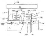
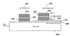
EEPROM이 가장 적용가능한, 소거의 소량의 인크리먼트를 갖고 더 큰 내구성(매우 높은 프로그램 및 소거 사이클을 견디는 능력)을 요구하는 어플리케이션에서, 2 트랜지스터 셀은 비휘발성 메모리 셀이 과소거되지 않도록 하는데 가장 적절하다. 도 5a-5c는 본 발명의 2 트랜지스터 메모리 셀을 도시한다. 메모리 셀(100)은 p형 기판(102) 상에 형성된다. n+ 드레인 영역(104) 및 n+ 소스 영역(106)은 p형 기판(102) 내에 형성된다.In applications where EEPROM is the most applicable, with a small amount of erase, and requires greater endurance (the ability to withstand very high program and erase cycles), two transistor cells are best used to ensure that non-volatile memory cells are not over-erased. proper. 5A-5C illustrate a two transistor memory cell of the present invention. The
비교적 얇은 터널링 옥사이드(108)는 p형 기판(102)의 표면 상에 증착된다. 다결정 실리콘 플로팅 게이트(poly-crystalline floating gate)(112)는 드레인 영 역(104) 및 소스 영역(106) 사이의 채널 영역(105) 위의 터널링 옥사이드(108)의 표면 상에 형성된다. 인터폴리 유전체층(interpoly dielectric layer)(114)은 컨트롤 게이트(116)를 형성하는 다결정 실리콘의 두번째 층으로부터 플로팅 게이트(112)를 분리하기 위해 플로팅 게이트(112) 상에 위치한다.Relatively
기본적으로 드레인 영역(104)은 선택 게이팅 트랜지스터(130)의 소스이다. 선택 게이팅 트랜지스터(130)의 드레인 영역(138)은 접촉부(124)를 통해 비트 라인(118)에 접속된다. 선택 게이팅 트랜지스터(130)의 게이트(140)는 메모리 셀(100)의 드레인 영역(104)과 선택 게이팅 트랜지스터(130)의 드레인 영역(138) 사이의 게이트 옥사이드(139) 위에 배치된다. 게이팅 장치의 옥사이드(139)는 프로그램 작동 동안 게이팅 장치의 게이트 상의 +18V를 견디기 위해 플로팅 게이트 장치(100)의 터널링 옥사이드(108) 보다 두껍다.Basically, drain
터널링 옥사이드(108)가 형성될 때, 더 두꺼운 게이트 옥사이드(139)는 메모리 셀(100)의 드레인 영역(104)과 선택 게이팅 트랜지스터(130)의 드레인 영역(138) 사이의 채널 영역에 형성된다. 게이트(140)는 메모리 셀의 과소거의 임펙트를 제어하기 위해 선택 신호를 선택 게이팅 트랜지스터(130)에 전달하는, 선택 컨트롤 라인(132)에 접속된다.When tunneling
2 트랜지스터 구성을 갖는 EEPROM 또는 플래쉬 메모리의, 대부분의 어플리케이션에서, p형 기판(102)은 대부분의 경우 접지 기준 포텐셜(0V)인, 전압을 바이어스하는 기판에 접속된다. 선택 게이팅 트랜지스터(130)의 드레인 영역(138)은 접촉부(124) 및 비트 라인 단자(118)를 통해 비트 라인 전압 발생기 6V에 접속된다. 컨 트롤 게이트(116)는 워드 라인 단자(120)를 통해 컨트롤 게이트 전압 발생기에 접속된다. 선택 게이트 라인(132)은 선택 게이팅 트랜지스터(130)의 게이트(140)에 선택 신호를 제공하기 위해 선택 신호 발생기에 접속된다. 소스 영역(106)은 소스 라인(122)과 소스 라인 전압 발생기에 접속된다.In most applications, such as an EEPROM or flash memory having a two transistor configuration, the p-
도 3a-3d의 2 트랜지스터 비휘발성 메모리 셀에 유사하게, 플로팅 게이트(112)는 채널 영역(105) 위에 드레인 영역(104) 및 소스 영역(106)의 에지(110)와 정렬되게 된다. 또한, 도 1d에 도시된 바와 같은 "윙"(28)이 없고 플로팅 게이트는 드레인 영역(104) 및 소스 영역(106)의 폭(128)으로 제한된다. 결합 계수는 따라서 도 2a-2c의 비휘발성 메모리 셀 이하(< 50%)이다.Similar to the two transistor nonvolatile memory cell of FIGS. 3A-3D, the floating
메모리 셀(100)은 메모리 셀(100)의 드레인 영역(104)에서 대략 +5V의 전압으로 전압을 설정함으로써 도 8b에 도시된 바와 같이 프로그램된다. 컨트롤 게이트(116)는 비교적 높은 양의 전압 레벨 (대략 +10.0V 내지 대략 +12.0V)에서 설정되고 소스 영역(106)은 접지된다. 드레인 영역(104) 및 채널(105)에서의 +5.0V는 선택 게이팅 트랜지스터(130)를 거쳐 비트 라인(118)으로부터 결합된다. 선택 게이트(SG)(132)를 통한 게이트(140)는 대략 +17.0V 내지 +22V의 전압에 설정된다. 이는 드레인 영역(104)의 높은 전압을 야기하고 채널(105)은 드레인 영역(104)로부터 플로팅 게이트(112)로 전자를 주사하는 CHE(Channel-Hot-Electron) 프로그래밍을 야기한다.The
선택 게이팅 트랜지스터(130)는 CHE 프로그램 작동 동안 대략 비트 라인(118)에서 +6V 및 셀의 드레인(104)에서 5V를 요구하기 때문에 본 발명의 2 트랜지 스터 EEPROM 메모리 셀 구조는 확장가능한 구조이다. 결과로서, 게이팅 장치(130)의 Vds를 걸쳐 약 1볼트의 전압 강하만이 있다. 게이팅 장치(130)에서 그러한 낮은 드레인 대 소스 전압(Vds) 요구 및 비트 라인(118)에서 낮은 전압(6V)는 선택 게이팅 트랜지스터(130)에서 더 높은 접합 파괴(junction breakdown) 및 더 큰 채널 길이를 강요하지 않는다. 그 결과, 소형의 게이팅 장치(130)는 0.13㎛ 이하의 기술에 적합한 폭과 동일한 피치의 플래쉬 메모리 셀(100) 내에서 달성될 수 있다.The two-transistor EEPROM memory cell structure of the present invention is an extensible structure because the
메모리 셀은 워드 라인과 따라서 컨트롤 게이트(116)가 -15.0V 내지 -22.0V에서 바이어스됨으로써 소거된다. 선택 게이팅 트랜지스터(130)를 통한 드레인 영역(104) 및 소스 라인(122)를 통한 소스 영역(106)은 모두 접지 기준 전압 레벨에서 유지된다. 선택 게이팅 트랜지스터(130)의 게이트(140)는 +3V로부터의 전압에서 배치되고 비트 라인(118)은 접지 기준 전압에서 배치되어 드레인(104)이 접지 기준 전압에 설정되는 것을 보장한다. 대안으로, 비트 라인(118) 및 소스 라인(122)은 부유하도록 강요될 수 있다.The memory cell is erased by biasing the word line and thus the
도 6은 EEPROM 어레이에서 도 5a-5c의 2 트랜지스터 비휘발성 메모리 셀의 어플리케이션을 도시한다. 2 트랜지스터 비휘발성 메모리 셀(100)의 그룹은 셀의 유닛(300a, ..., 300k, 305a, ..., 305k)에 정렬된다. 상기 유닛은 일반적으로 바이트이나, 행 및 열로 정렬된다. 플래쉬 메모리에서, 메모리 셀은 도 3a-3d에 도시된 바와 같은 공통의 p형 기판을 갖는 단일 그룹일 수 있다. 셀의 유닛(300a, ..., 300k, 305a, ..., 305k)은 임의의 트리플 웰 없이 p-기판에 형성되는 바람직한 실시예에서 구성된다. 어레이의 각 행의 각각의 비휘발성 메모리 셀(100)의 컨트롤 게이트는 하나의 워드 라인(325a, ..., 325k, 327a, ..., 327k)에 접속된다. 유사하게, 어레이의 각 행의 각각의 비휘발성 메모리 셀(100)의 소스는 하나의 소스 라인(330a, ..., 330k, 332a, ..., 332k)에 접속된다. 어레이의 각 열의 각각의 비휘발성 메모리 셀(100)의 드레인은 하나의 비트 라인(345a, ..., 345m, 350a, ..., 350m)에 접속된다.6 illustrates an application of the two transistor nonvolatile memory cell of FIGS. 5A-5C in an EEPROM array. The group of two transistor
각 유닛(300a, ..., 300k, 305a, ..., 305k)의 각각의 비휘발성 메모리 셀(100)은 게이팅 트랜지스터의 드레인에 의해 메모리 셀(100)의 게이팅 트랜지스터를 통해 마스터 비트 라인(345a, ..., 345m, 350a, ..., 350m)에 접속된다. 각 행의 유닛(300a, ..., 300k, 305a, ..., 305k)의 각 메모리 셀에 대한 게이팅 트랜지스터의 게이트는 선택 게이트 라인(320a, ..., 320k)에 접속된다. 각 유닛(300a, ..., 300k, 305a, ..., 305k)에 대한 소스 라인(330a, ..., 330k, 332a, ..., 332k)는 마스터 소스 라인(340a 및 340m)에 각각 접속된다.Each
다시 도 8b를 참조하면, 선택된 셀의 프로그래밍은 개별적인 셀에 대해 설명된 바와 같다. 프로그램될 셀을 포함하는 워드 라인(325a, ..., 325k, 327a, ..., 327k) (각각의 선택된 유닛 (바이트) 내 워드 라인 당 다중 셀이 프로그램될 수 있다)은 (+10.0V 내지 +12.0V와 비슷한) 비교적 높은 전압에서 활성화된다. 게이트 라인(320) 및 따라서 프로그램될 셀의 유닛(300a, ..., 300k, 305a, ..., 305k)의 메모리 셀(100)의 게이팅 트랜지스터의 게이트는 (+15.0V 내지 +22.0V와 비슷한) 매우 높은 전압에 설정되어 셀의 유닛(300a, ..., 300k, 305a, ..., 305k)의 메모리 셀(100)의 게이팅 트랜지스터를 활성화시킨다. 선택된 비휘발성 메모리 셀(100) 을 포함하는 열의 비트 라인(345a, ..., 345m, 350a, ..., 350m)은 (6V와 비슷한) 적당히 높은 전압으로 설정된다. 마스터 소스 라인(340a, ..., 340m)은 접지 기준 전압(0V)에 설정된다. 전술된 바와 같이 이는 선택된 비휘발성 메모리 셀(100)의 플로팅 게이트의 채널 열전자 충전을 일으킨다.Referring again to FIG. 8B, the programming of the selected cell is as described for the individual cell.
프로그램되지 않은 선택된 비휘발성 메모리 셀(상기 셀들은 소거에 의해 논리 1에 설정됨)을 포함하지 않는 비트 라인(345a, ..., 345m, 350a, ..., 350m)은 접지 기준 포텐셜에 설정된다. 선택 게이트 라인(320a, ..., 320k)은 매우 높은 전압 레벨(+15.0V 내지 +22.0V)에 설정되어 선택된 비휘발성 메모리 셀(100)을 포함하지 않는 상기 비트 라인(345a, ..., 345m, 350a, ..., 350m)에 대해 메모리 셀(100)의 선택 게이팅 트랜지스터를 활성화시킨다. 따라서 선택된 비휘발성 메모리 셀을 포함하지 않는 비트 라인(345a, ..., 345m, 350a, ..., 350m) 상에 없는 선택되지 않은 메모리 셀의 드레인은 접지 기준 포텐셜(0V)에 설정된다.
선택된 비휘발성 메모리 셀을 포함하는 워드 라인(325a, ..., 325k, 327a, ..., 327k) 상의 선택되지 않은 비휘발성 메모리 셀은 비교적 높은 전압(+10.0V 내지 +12.0V)에 설정된 자체 컨트롤 게이트를 구비한다. 선택되거나 선택되지 않은 블록의 비휘발성 메모리 셀 각각의 소스는 접지 기준 포텐셜(0V)에 설정된다.The unselected nonvolatile memory cells on
선택된 비휘발성 메모리 셀을 포함하는 비트 라인(345a, ..., 345m, 350a, ..., 350m) 상의 선택되지 않은 비휘발성 메모리 셀은 비교적 높은 전압(+6V)에 설정된 자체 드레인을 구비한다. 플로팅 게이트를 구비한 트랜지스터의 소스 및 게이트는 접지 기준 포텐셜(0V)에 설정되기 때문에, 채널 열전자 현상은 발생되지 않고 따라서 선택되지 않은 비휘발성 메모리 셀(100)을 방해하지 않는다.Unselected nonvolatile memory cells on
선택된 셀의 유닛(300a, ..., 300k, 305a, ..., 305k)에 있지 않은 상기 비휘발성 메모리 셀은 선택되지 않은 유닛(300a, ..., 300k, 305a, ..., 305k) 내 임의의 방해 신호를 방지하기 위해 접지 기준 포텐셜(0V)에 설정된 자체 선택 게이트 라인(320a, ..., 320k), 워드 라인(325a, ..., 325k, 327a, ..., 327k), 소스 라인(330a, ..., 330k, 332a, ..., 332k), 및 비트 라인(345a, ..., 345m, 350a, ..., 350m)을 구비하지 않는다.The nonvolatile memory cells that are not in
소거는 메모리 셀(100)의 전체 유닛(300a, ..., 300k, 305a, ..., 305k) 또는 메모리 셀(100)의 유닛(300a, ..., 300k, 305a, ..., 305k)의 그룹에 대해 발생하고 개별 셀에 대해 설명된 바와 본질적으로 같다. 메모리 셀(100)의 선택된 유닛(또는 유닛들)(300a, ..., 300k, 305a, ..., 305k) 내 워드 라인(325a, ..., 325k, 327a, ..., 327k)은 (-15.0V 내지 -22.0V와 비슷한) 비교적 큰 음의 전압에 설정된다. 선택된 유닛(300a, ..., 300k, 305a, ..., 305k)의 선택 게이트 라인(320a, ..., 320k) 및 메모리 셀(100)의 게이팅 트랜지스터의 게이트는 접지 기준 포텐셜(0V)에 설정되어 메모리 셀(100)의 게이팅 트랜지스터를 비활성화한다. 선택된 유닛(300a, ..., 300k, 305a, ..., 305k)의 비트 라인(345a, ..., 345m, 350a, ..., 350m)은 접지 기준 포텐셜(0V)에 설정된다. 마스터 소스 라인(340a, ..., 340m) 및 선택된 유닛(300a, ..., 300k, 305a, ..., 305k)의 소스 라인(330a, ..., 330k, 332a, ..., 332k)은 접지 기준 전압(0V)에 설정된다. 전술된 바와 같이 이는 플로팅 게이트로부터 전하의 Fowler-Nordhem 터널링을 일으켜 선택된 유닛(300a,..., 300k, 305a,..., 305k)의 비휘발성 메모리 셀(100)의 플로팅 게이트로부터 모든 전하를 제거 한다.Erasing may be performed on the
선택된 유닛(300a, ..., 300k, 305a, ..., 305k)의 모든 비휘발성 메모리 셀(100)은 소거되기 때문에, 선택된 비휘발성 메모리 셀(100)의 동일한 유닛(300a,..., 300k, 305a,..., 305k)에 있지 않은 상기 비휘발성 메모리 셀은 서브어레이 내 임의의 방해 신호를 방지하기 위해 접지 기준 포텐셜(0V)에 설정된 자체 선택 게이트 라인(320a, ..., 320k), 워드 라인(325a, ..., 325k, 327a, ..., 327k), 및 비트 라인(345a, ..., 345m, 350a, ..., 350m)을 구비한다.Since all
도 7은 선택 게이팅 트랜지스터의 채널 폭과 도 4의 게이팅 트랜지스터(210a,..., 210m, 215a,..., 215m)에 대한 자체 게이트 전압 또는 도 5a-5c의 2 트랜지스터 비휘발성 메모리 셀 각각의 선택 게이팅 트랜지스터(130) 사이의 관계를 도시하는 플롯이다. 메모리 어레이의 전하 펌프 회로의 비트 라인 전압 발생기는 비트 라인을 대략 6.5V의 전압에 설정한다. 이는 메모리 셀이 채널 열전자 프로그래밍을 수행하는데 드레인 전압 5V 및 드레인 전류 500㎂를 필요로 한다는 가정하에 의한 것이다. 선택 게이팅 트랜지스터는 0.4㎛에 고정된 채널 길이를 갖도록 설계된다. 상기 플롯은 상이한 게이트 전압 하에서 상기의 요구되는 조건을 제공하기 위해 요구되는 최소 채널 폭을 도시한다. 채널 폭은 컨트롤 게이트가 전압 10V에 설정되는 종래 기술의 비휘발성 메모리 셀에 대해 1.7㎛여야 함을 보여준다. 그러나, 본 발명의 메모리 셀의 컨트롤 게이트 전압에 대해, 인가되는 전압은 20V로 증가된다. 이는 선택 게이팅 트랜지스터의 채널 폭이 단지 0.45㎛로 급격히 감소될 수 있도록 한다. 이는 선택 게이팅 트랜지스터가 메모리 셀의 피치(어레이 내 메모리 셀의 열의 폭)에 맞춰지기에 충분히 작은 크기를 갖도록 한다. EEPROM 어레이 내에 구성된 2 트랜지스터 비휘발성 메모리 셀은 본 발명의 플래쉬 메모리 어레이 내에 구성된 단일 트랜지스터 비휘발성 메모리 셀과 동일한 메모리 셀 구조를 포함한다. 두 어레이 구조는 동일한 Fowler-Nordhem 채널 소거 및 채널 열전자 프로그램 구성을 사용한다. 이는 기판 상의 동일한 집적 회로 내에 EEPROM 어레이 구조와 플래쉬 메모리 어레이 구조의 통합을 허용한다.7 shows the channel width of the select gating transistor and its own gate voltage for the
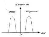
도 9a 및 도 9b는 본 발명의 비휘발성 메모리 셀의 전압 임계값 그룹의 분포를 도시한다. 읽기 작동(Vread) 동안 기준 임계 전압으로 사용된 전압은 비휘발성 메모리 셀에 대해 소거된 (논리 1) 및 프로그램된 (논리 0) 사이의 경계로서 규정된다. 소거 동안 플로팅 케이트로부터 제거된 전하의 양 또는 프로그래밍 동안 플로팅 게이트 상에 위치된 전하의 양은 변하기 때문에, 비휘발성 메모리 셀에 대한 전압 임계값은 도시된 바와 같은 분포를 갖는다. 어레이의 선택된 비휘발성 메모리 셀을 포함하는 비트 라인은 선택된 비휘발성 메모리 셀이 프로그램되는지 또는 소거되는지 여부를 검출하기 충분한 전압에 설정되고 선택된 비휘발성 메모리 셀을 포함하는 워드 라인은 기준 임계 값(Vread)에 위치한다. 선택된 비휘발성 메모리 셀이 소거되면, 선택된 비휘발성 메모리 셀은 턴온(turn on)되고 논리 1이 검출된다. 대안으로, 선택된 비휘발성 메모리 셀이 프로그램되면, 선택된 비휘발성 메모리 셀은 턴온되지 않고 논리 0이 검출된다.9A and 9B show the distribution of voltage threshold groups of nonvolatile memory cells of the present invention. The voltage used as the reference threshold voltage during the read operation Vread is defined as the boundary between erased (logic 1) and programmed (logic 0) for the nonvolatile memory cell. Since the amount of charge removed from the floating gate during erase or the amount of charge located on the floating gate during programming varies, the voltage threshold for the nonvolatile memory cell has a distribution as shown. The bit line containing the selected nonvolatile memory cells of the array is set to a voltage sufficient to detect whether the selected nonvolatile memory cell is programmed or erased, and the word line comprising the selected nonvolatile memory cell has a reference threshold (Vread). Located in When the selected nonvolatile memory cell is erased, the selected nonvolatile memory cell is turned on and
전술된 바와 같이, 프로그램(소거)되지 않고 다음으로 반복되는 소거 작동에 의존하는 상기 비휘발성 메모리 셀은 도 9b에 도시된 바와 같이 과소거될 수 있다. 역으로, 더빠른 소거 속도를 갖는 비휘발성 메모리 셀의 블록 내 상기 비휘발성 메모리 셀은 또한 과소거에 의존할 수 있다. 비휘발성 메모리 셀의 플로팅 게이팅 트랜지스터는 본래 증가형(enhancement mode)에서 작동하고 항상 (턴온되어) 수행한다. 이러한 조건은 도 3a-3d의 단일 트랜지스터 플래쉬 비휘발성 메모리 셀에 대해 허용될 수 없다. 그러나, 도 5a-5c의 2 트랜지스터 EEPROM 비휘발성 메모리 셀은 과소거된 셀을 허용하고 개선된 플로팅 게이팅 트랜지스터를 통해 비트 라인의 전류 흐름을 방지함으로써 다른 셀의 데이터 손상을 방지한다. "정정(correction)", "교정(repair)", "복구(recover)", "수렴(converge)", 또는 "소프트-프로그래밍(soft-programming)"으로 칭해지는 특정 작동은 상기 과소거된 비휘발성 메모리 셀의 임계 전압을 플래쉬 메모리 셀에 대해 원하는 기준 임계 전압(Vread) 상에 중심이 오도록 다시 조정하기 위해 채용될 수 있다.As described above, the nonvolatile memory cells that are not programmed (erase) and rely on the next repeated erase operation may be over-erased as shown in Fig. 9B. Conversely, the nonvolatile memory cell in the block of nonvolatile memory cells with faster erase speed may also depend on over erasure. Floating gating transistors in non-volatile memory cells inherently operate in enhancement mode and always perform (turned on). This condition is not acceptable for the single transistor flash nonvolatile memory cell of FIGS. 3A-3D. However, the two-transistor EEPROM nonvolatile memory cells of FIGS. 5A-5C prevent data corruption in other cells by allowing the over-erased cell and preventing current flow in the bit line through the improved floating gating transistor. Certain operations, referred to as "correction", "repair", "recover", "converge", or "soft-programming", may be used to provide The threshold voltage of the volatile memory cell can be employed to readjust to center on the desired reference threshold voltage Vread for the flash memory cell.
본 발명의 단일 트랜지스터 플래쉬 비휘발성 메모리 셀 및 2 트랜지스터 EEPROM 비휘발성 메모리 셀은 EEPROM 및 플래쉬 메모리와 같은 어플리케이션에 동일한 구조를 사용하기 때문에, 프로그램밍 및 소거 시간의 양이 동일할 수 있다. 사실상, 플래쉬 소거 시간은 약 수백 mS이고, 반면 EEPROM은 제품 규격에서 수 mS이다. 두 메모리는 모두 프로그래밍을 위해 동일한 CHE 구성을 사용하기 때문에, 프로그램 시간은 오늘날 제품 규격의 1㎲ 내지 10㎲ 범위와 동일하다. 도 10은 본 발명의 비휘발성 메모리 셀에 대한 프로그램 및 소거 시간에 대한 것이다. 채널 열전자 프로그래밍으로 임계 전압을 변경시키는 시간의 양이 플롯(90)에 도시된다. 비휘발성 메모리 셀을 소거하기 위해 Fowler Nordheim 터널링으로 플로팅 게이트로부터 전하를 제거하는 시간의 양은 플롯(95)에 도시된다. 비휘발성 메모리 셀의 프로그래밍에 대해 설명된 바와 같이 필요한 전압의 어플리케이션에 대한 시간은 대략 1㎲ 내지 10㎲의 지속 시간을 갖는다. 비휘발성 메모리 셀의 소거는 대략 1㎳ 내지 1s의 지속 시간을 갖는다.Since the single transistor flash nonvolatile memory cell and the two transistor EEPROM nonvolatile memory cell of the present invention use the same structure for applications such as EEPROM and flash memory, the amount of programming and erase time can be the same. In fact, the flash erase time is about several hundred mS, while the EEPROM is several mS in the product specification. Since both memories use the same CHE configuration for programming, program time is the same as the 1 ㎲ to 10 ㎲ range of today's product specifications. 10 is a program and erase time for a nonvolatile memory cell of the present invention. The amount of time for changing the threshold voltage with channel thermoelectronic programming is shown in
도 11a-11m은 도 4의 플래쉬 메모리 구조의 게이팅 트랜지스터(210a, ..., 210m, 215a, ...,215m)와 비휘발성 메모리 셀(100) 또는 도 5a-5c의 2 트랜지스터 비휘발성 메모리 셀의 게이팅 트랜지스터(130)의 제조 방법을 도시한다. 상기 도면에서, 플로팅 게이팅 트랜지스터(100) 및 선택 게이팅 트랜지스터(130)는 두개의 다결정 실리콘 층(폴리-1 및 폴리-2)을 구성하는 적층된 게이트 구조를 갖으나 셀(100)의 컨트롤 게이트(116) 및 플로팅 게이트(112)만이 인터-폴리 유전체(114)에 의해 분리된다. 선택 게이팅 장치(130)의 폴리-2 컨트롤 게이트 및 폴리-1 플로팅 게이트는 분리 없이 단축된다. 플로팅 게이팅 트랜지스터(100)에 대해, 폴리-1은 플로팅 게이트로서 사용되고, 폴리-2는 컨트롤 게이트로서 사용된다. 선택 게이팅 트랜지스터(130)는 또한 스택 게이트 구조를 갖으나, 게이트 전압은 직접 폴리-1 층에 인가된다.11A-11M are gating
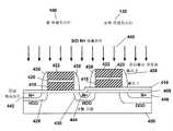
도 11a에서, <100> 결정학적 방향(crystallographic orientation)을 갖는 p형 실리콘 기판(400)이 제공된다. 임플란트 옥사이드(402)는 다음으로 약 100Å 내지 300Å 사이의 두께로 증착 또는 열산화(thermal oxidation)에 의해 실리콘 기판(400) 상에 형성된다. 다음으로 감광제 층(404)은 선택 게이팅 트랜지스터(130) 영 역의 마스크에 의해 증착되고 패턴화된다. 다음으로 선택 게이팅 트랜지스터(130) 영역은 임계 전압 조정값(Vt) 임플란트로 임플란트 되고(406) 이어 필드 임플란트에 의해 임플란트된다. 두 임플란트 모두 선택 게이팅 트랜지스터(130)의 임계 전압 및 필드 트랜지스터 턴-온 전압을 조정하기 위해 붕소(boron) 또는 BF2(boron difluoride)와 같은 p형 불순물(p-type impurity)을 사용한다. 선택 게이팅 트랜지스터(130)의 임계 전압은 약 0.6 내지 1.5V 사이이고, 필드 트랜지스터의 임계 전압은 일반적으로 18V보다 크다. 선택 게이팅 트랜지스터(130) Vt 임플란트는 약 5 내지 50KeV 사이의 임플란트 에너지 및 붕소 이온을 사용하여 약 3E11 내지 5E12 이온/㎠ 사이의 선량(dose)을 갖는다. 선택 게이팅 트랜지스터(130)에 대한 필드 임플란트(406)는 약 30 내지 180KeV 사이의 에너지 및 붕소 이온을 사용하여 약 1E12 내지 1E14 이온/㎠ 사이의 선량을 갖는다. 필드 임플란트는 선택 게이팅 트랜지스터(130) Vt 임플란트보다 더 높은 임플란트 에너지를 갖는데, 이는 임플란트된 이온들이 필드 옥사이드를 통과해야 할 필요가 있기 때문이다. 프로그램 동안, 선택 게이트 전압은 약 15-22V 사이이고, 이는 워드 라인 전압보다 높다. 그러므로 필드 임플란트는 선택 게이트가 높은 전압을 갖을 때 필드 트랜지스터가 턴 온되지 않도록 보장하기 위해 필드 트랜지스터의 임계 전압을 증가시키도록 요구된다.In FIG. 11A, a p-
감광제(404) 및 임플란트 옥사이드(402)가 스트립된 후, 약 100 내지 300Å 사이의 두께를 갖는 고전압(HV) 게이트 옥사이드(408) 층이 다음으로 도 11b에서 도시된 바와 같이 실리콘 기판(400) 상에서 열적으로 성장된다. 실리콘 기판(400) 은 다음으로 감광제(410)를 형성하기 위해 셀 트랜지스터 포토리소그래피에 의해 패턴화된다. 플로팅 게이팅 트랜지스터(100) 영역은 비휘발성 메모리 셀 트랜지스터(100) Vt 임플란트 및 필드 임플란트로 임플란트된다(412). 셀 Vt 임플란트는 약 1.0 내지 3.0V 사이의, 비휘발성 메모리 셀 트랜지스터(100)의 임계 전압을 조정하기 위해 사용된다. 필드 임플란트는 도면에 도시되지 않은 N-필드 트랜지스터의 임계 전압을 20.0V보다 높게 증가시키는 것이다. 비휘발성 메모리 셀 트랜지스터(100) Vt 임플란트는 약 5 내지 50KeV 사이의 에너지 및 붕소 이온을 사용하여 약 1E12 내지 1E13 이온/㎠ 사이의 선량을 갖는다. 필드 임플란트는 약 30 내지 180KeV 사이의 에너지 및 붕소 이온을 사용하여 약 1E12 내지 1E14 이온/㎠ 사이의 선량을 갖는다.After the
다음으로 HV 게이트 옥사이드(408)는 도 11d에 도시된 바와 같이 비휘발성 메모리 셀 트랜지스터(100) 영역에서 제거된다. 다음으로 감광제(414)가 제거된다. 다음으로 약 70 내지 120Å 사이의 두께를 갖는 터널 옥사이드(408)는 도 11e에서 도시된 바와 같이 약 900 내지 1100℃ 사이의 온도에서 종래의 건식 산화(dry oxidation) 공정에 의해 실리콘 웨이퍼 상에서 열적으로 성장된다. 선택 게이팅 트랜지스터(130) 상에서 성장된 터널 옥사이드(416)는 비휘발성 메모리 셀 트랜지스터(100) 영역 상에서 성장된 옥사이드보다 더 얇으며, 이는 HV 게이트 옥사이드(408)가 이미 그 영역 상에 존재하기 때문이다. 터널 옥사이드(416) 및 HV 게이트 옥사이드(408)는 결합되어 약 150 내지 350Å 사이의, 선택 게이팅 트랜지스터(130)에 대한 게이트 옥사이드가 된다.
도 11f에서, 다음으로 제1 폴리실리콘 층(폴리 1)(418)이 LPCVD 공정을 사용하여, 약 1000 내지 2000Å 사이의 두께에서 증착된다. 다음으로 폴리실리콘 층(418)은 폴리-1 사진(photo)에 의해 패턴화된다. 폴리-1 윈도우 내 폴리실리콘 층(418)은 제거된다.In FIG. 11F, a first polysilicon layer (Poly 1) 418 is then deposited at a thickness between about 1000 and 2000 microns using an LPCVD process. The
다음으로 실리콘 디옥사이드(silicon dioxide), 실리콘 니트라이드(silicon nitride), 또는 옥사이드(oxide)/니트라이드(nitride)/옥사이드 화합물(oxide composition) 층과 같은, 인터-폴리실리콘 유전체층(420)이 LPCVD(low pressure chemical vapor deposition), PECVD(plasma enhanced chemical vapor deposition), 또는 HDPCVD(high density plasma chemical vapor deposition)을 사용하여 증착되거나, 또는 열 산화 공정이 또한 실리콘 옥사이드 옵션을 형성하기 위해 사용될 수 있으며, 도 11g에 도시된 바와 같이 모두 약 100 내지 300Å 사이의 두께가 된다. 이어서 도 11h에 도시된 바와 같이 제2 폴리실리콘층(422)의 증착이 LPCVD 공정을 사용하여, 약 1500 내지 3000Å 사이의 두께에서 이루어지고, 다시 그 위치에, 증착 동안, 아르신(arsine), 포스핀(phosphine)의 첨가를 통해, 시레인 엠비언트(silane ambient)로 도핑되거나, 또는 비휘발성 메모리 셀(100)의 컨트롤 게이트에 대해 이어서 사용될 WSi(Tungsten silicide) 층이 추가된다.Next, the
다음으로 포토리소그래픽 및 RIE(reactive ion etching) 공정이 채용되어, 도 11i의 단면도에 개략적으로 도시된, 폴리 1(418) 및 폴리 2(422) 층을 갖는 적층된 게이트 구조를 형성한다. 이방성 RIE 공정은 제1 폴리실리콘층(418) 및 제2 폴리실리콘층(422)에 대해 염소(Cl2)를 사용하여 수행되고, 반면 기체 CHF3를 함유하는 불소(fluorine)는 인터-폴리실리콘 유전체층(420)을 패턴화하는데 사용된다. 비휘발성 메모리 셀(100)의 적층된 게이트 구조물은 제2 폴리실리콘층(422), 인터-폴리실리콘 유전체층(420)으로 형성된 컨트롤 게이트, 및 제1 폴리실리콘층(418)으로 형성된 플로팅 게이트를 구비한다. 전술된 바와 같이 적층된 게이트 구조물은 터널 옥사이드층(416) 상에 존재한다.Photolithographic and reactive ion etching (RIE) processes are then employed to form a stacked gate structure with
도 11j에서, 감광제층(424)이 증착된다. 메모리 셀 포토 마스크는 비휘발성 메모리 셀(100) 영역을 지정하고, 이로부터 감광제가 제거된다. 다음으로 비휘발성 메모리 셀 소스(428) 및 드레인(430) 접합이 비소 이온(arsenic ions)을 사용하여, 약 30 내지 60KeV 에너지에서, 약 1E15 내지 7E15 이온/㎠ 사이의 선량에서, 이온 주입법(ion implantation)(426) 공정을 통해 형성된다. 비휘발성 메모리 셀 드레인(430) 접합은 채널 열전자의 임팩트 이온화를 촉진시키는 계단 접합(abrupt junction)이다. 메모리 셀 임플란트(426)는 셀 드레인에 대해 대량으로 도핑된 드레인(HDD) 접합을 형성하는 것이다. 또한 비휘발성 메모리 셀 소스(428) 및 드레인(430)은 비휘발성 메모리 셀(100)의 컨트롤 게이트 및 플로팅 게이트의 적층된 게이트 구조물의 에지와 정렬하도록 구조화된다. 도 3d에 표시된 바와 같이, 적층된 게이트 구조물은 비휘발성 메모리 셀의 경계를 정하는 STI(shallow trench isolation)(미도시) 내로 제한된다.In FIG. 11J, a
도 11k에서 도시된, 선택 게이팅 트랜지스터(130)의 드레인 접합부(436)는 비휘발성 메모리 셀 드레인(430) 접합부보다 더 높은 접합 파괴 전압을 유지하도록 요구한다. 반면에, 선택 게이팅 트랜지스터(130)의 드레인(430) 접합부 근처의 충격 이온화는 바람직하지 않다. 선택 게이팅 트랜지스터(130)의 드레인 접합부(436)는 비휘발성 메모리 셀 드레인(430) 접합부와 상이한 도핑 프로파일을 갖는다. 선택 게이팅 트랜지스터 드레인(436) 영역은 선택 게이팅 트랜지스터(130) 포토 마스크(432)에 의해 규정되고, 약 50 내지 150KeV 에너지에서, 약 1E14 내지 2E15 이온/㎠ 사이의 선량에서, 인 이온(phosphorus ions)으로 임플란트된다(434). 임플란트(434)는 선택 게이팅 트랜지스터(130) 드레인에 대한 DDD(double diffused drain) 접합부(436)를 형성하는 것이다. DDD 접합부(436)는 메모리 셀 드레인(430) 접합부보다 더 단계적인 도핑 프로파일을 갖는다.The
도 11l에 개략적으로 도시된, 절연체 스페이서(438)는 LPCVD 또는 PECVD 공정을 통해, 약 1000 내지 2000Å 사이의 두께에서, 실리콘 나트라이드와 같은 절연체층의 증착을 통해 형성되고, 이에 이어서, 식각재료(etchant)로서 불소계 화합물(fluorine based compound)(CF4)를 사용하여, 이등방성의 RIE 공정이 수행된다. 다음으로 소스/드레인 n+ 임플란트(440)는 소스/드레인(442, 444, 446) 직렬 저항을 감소시키기 위해 비소 또는 인 이온을 사용하여 약 5E14 내지 1E16 이온/㎠ 사이의 선량에서, 약 30 내지 60KeV 사이의 에너지에서, 이온 주입 공정을 통해 임플란트된다.The
상기 과정은 약 8000 내지 15000Å 사이의 두께에서, LPCVD 또는 PECVD 공정 을 통해 획득된, 실리콘 디옥사이드로 구성된, ILD(interlevel dielectric)층을 증착함으로써 계속된다. ILD는 적층된 게이트 구조물 사이의 공간을 완전히 채운다. 다음으로 ILD층의 평탄화가 CMP(chemical mechanical planarization)를 통해 달성되어, 소스/드레인 영역으로의 개구를 위해 사용되는, 연속의, 포토리소그래픽 공정의 엄격함을 감소시켜, ILD층에 대한 매끄러운 상부 표면 토폴로지로 된다. 접촉 홀 개구는 CHF3와 같은 플로린계 식각재료를 사용하여, ILD 층의 RIE 공정을 통해 형성된다. 텅스텐과 같은 금속층은, 약 3000 내지 4000Å 사이의 두께에서, 소스와 같은 텅스텐 헥사플루오라이드(tungsten hexafluoride)를 사용하여, LPCVD 공정을 거쳐 증착되거나, 또는 접촉 홀 개구를 완전히 채우는, RF 스퍼터링 공정을 거쳐 증착된다. ILD층의 상부 표면 상에 존재하는, 텅스텐 층의 제거는 CMP 공정을 통해, 또는 식각 재료로서 Cl2를 사용하는, 선택적인 RIE 공정을 통해 달성된다. 텅스텐 플러그는 소스, 드레인, 및 폴리실리콘 게이트에 전기 접촉을 제공하는 것이다. 다음으로 알루미늄 층과 같은 금속층이 제1 금속 상호접속부를 제공하기 위해 약 3000 내지 8000Å 사이의 두께로, RF 스퍼터링을 통해 증착된다.The process continues by depositing an interlevel dielectric (ILD) layer composed of silicon dioxide, obtained through an LPCVD or PECVD process, at a thickness between about 8000 and 15000 kPa. The ILD completely fills the space between the stacked gate structures. Next, planarization of the ILD layer is achieved through chemical mechanical planarization (CMP), which reduces the stringency of the continuous, photolithographic process used for openings to the source / drain regions, resulting in a smooth top surface for the ILD layer. It becomes a topology. Contact hole openings are formed through the RIE process of the ILD layer using a florin-based etching material such as CHF3 . A metal layer, such as tungsten, is deposited via an LPCVD process, using a tungsten hexafluoride, such as a source, at a thickness between about 3000 and 4000 microns, or via an RF sputtering process, which completely fills the contact hole openings. Is deposited. Removal of the tungsten layer, present on the top surface of the ILD layer, is accomplished through a CMP process or through an optional RIE process, using Cl2 as an etching material. Tungsten plugs provide electrical contact to the source, drain, and polysilicon gates. Next, a metal layer, such as an aluminum layer, is deposited via RF sputtering, with a thickness between about 3000 and 8000 kHz to provide a first metal interconnect.
선택 게이팅 트랜지스터의 적층된 게이트 구조물(418, 420, 및 422)은 도 6의 선택 게이트 라인(320a, ..., 320k)에 폴리 1 게이트의 외부 접속부를 갖는다. 도시된 바와 같이 비휘발성 메모리 셀 및 선택 게이팅 트랜지스터에 대한 프로세스 단계는 임의의 현재 반도체 프로세스의 병렬작업 반도체 프로세스(concurrent semiconductor process)에 의해 수행될 수 있고 장래에 이용가능할 수 있는 프로세 스 단계에서 진보된 것이 적용될 수 있다. 고전압 관련 신뢰성 문제는 채널 길이, 게이트 옥사이드 두께, STI 깊이 등과 같은 셀 구조물의 파라미터를 주의하여 선택함으로써 최적화될 수 있다. NAND형 어레이 플래쉬 메모리 비휘발성 셀의 현재 반도체 프로세싱은 매우 높은 신뢰성을 갖는 것으로 입증되었다. 상기 프로세스는 본 발명의 비휘발성 메모리 셀 제조에 충분한, 백만 이상의 사이클 내구성을 갖고 20V 이상 유지할 수 있다.The
제조 프로세스의 변형예가 도 12a-12c에서 설명된다. 상기 변형예는 자기-정렬 프로세스(self-aligned process)로서, 제1 폴리실리콘이 필드 옥사이드에 자기-정렬되어 도 3d에 도시된 바와 같이 비휘발성 셀 크기의 폭을 비휘발성 메모리 셀(100)의 소스 및 드레인의 폭으로 감소시킨다. 도 3d의 STI(126)는 제1 폴리실리콘(418) 증착 후 형성되어 제1 폴리실리콘(418)이 도 12a의 비휘발성 메모리 셀(100)의 액티브 에지에 자기-정렬된다.A variant of the manufacturing process is described in FIGS. 12A-12C. The modification is a self-aligned process in which the first polysilicon is self-aligned to the field oxide so that the width of the nonvolatile cell size of the
제1 폴리실리콘층(418)의 증착 및 형성은 LPCVD 또는 PECVD와 같은 공지의 프로세스에 의해 이루어져 전술된 바와 같은 터널 옥사이드 상에 대략 500-650Å 두께의 폴리실리콘 층이 된다. 바람직하게 1500Å의 실리콘 니트라이드층은 CVD에 의해 증착된다. 액티브 영역의 포토 마스크는 절연 형성 동안 액티브 영역을 규정하기 위해 사용된다. 감광제층은 실리콘 니트라이드층 상에 도포되고 마스킹 단계는 실리콘 니트라이드, 제1 폴리실리콘, 및 선택적 영역의 아래 절연층을 에칭하여 수행된다. 감광제가 제거되지 않는 경우, 이는 실리콘 니트라이드, 제1 폴리실리콘 영역, 및 아래의 절연 물질 영역의 상부에 남는다. 감광제가 제거되는 경우, 이는 실리콘 니트라이드, 제1 폴리실리콘, 및 아래의 절연 물질은 에칭된다. 절연 영역을 형성하는데에는 두가지 방법이 있다: 실리콘의 국부 산화(local oxidation of silicon: LOCOS) 및 STI. STI 방법에서, 에칭은 대략 2800~3200Å의 깊이까지 기판으로 계속된다. 실리콘 트랜치는 실리콘 디옥사이드와 같은 절연 물질로 채워진다. 이는 로컬 필드 옥사이드가 되는 공지의 LOCOS 프로세스일 수 있거나 또는 영역 내에 형성된 실리콘 디옥사이드가 되는 STI 프로세스일 수 있다. 바람직한 방법에서, 얕은 트랜치가 형성될 것이다. STI는 제1 폴리실리콘층(418)에 대해 평탄하게 형성될 수 있기 때문에 바람직하다. 비휘발성 메모리 셀(100)의 플로팅 게이트(418) 구조물은 비휘발성 메모리 셀(100)의 소스 및 드레인에 자기-정렬된다.The deposition and formation of the
절연 영역이 형성된 후, 다음으로 실리콘 디옥사이드, 실리콘 니트라이드, 또는 옥사이드/니트라이드/옥사이드 화합물과 같은 인터-폴리실리콘 유전체층(420)이 LPCVD, PECVD, 또는 HDPCVD를 사용하여 증착되거나, 또는 열 산화 공정이 실리콘 옥사이드 옵션을 형성하는데 또한 사용될 수 있고, 모두 도 12a에 도시된 바와 같이 약 100 내지 300Å 사이의 두께가 된다. 다음으로 인터-폴리실리콘 유전체층(420)은 ONO(oxide-nitride-oxide)의 포토 마스크에 의해 패턴화된다. 인터-폴리실리콘 유전체층(420)은 도 12b에서 도시된 바와 같이 플루오르 화합물(CHFx)을 사용하는 이방성의 RIE 공정에 의해 선택 게이팅 트랜지스터(130)에서 제거된다. 제2 폴리실리콘층(422)은 도 11h에서 설명된 바와 같이, LPCVD 공정을 사용하여, 약 1500 내지 3000Å 사이의 두께에서 증착되고, 다시 그 위치에, 증착 동안, 아르신 (arsine), 포스핀(phosphine)의 첨가를 통해, 시레인 엠비언트(silane ambient)로 도핑되거나, 또는 비휘발성 메모리 셀의 컨트롤 게이트에 대해 이어서 사용될 WSi(Tungsten silicide) 층이 추가된다.After the insulating region is formed, an
다음으로 포토리소그래픽 및 RIE 공정이 채용되어, 도 12c의 단면도에 개략적으로 도시된, 적층된 게이트 구조물(418, 420, 및 422)을 형성한다. 제2 폴리실리콘층(422)이 증착되어 선택 게이팅 트랜지스터(130)에 대한 게이트를 형성하기 위해 제1 폴리실리콘층(418)과 직접 전기 접촉한다.Photolithographic and RIE processes are then employed to form stacked
단일 및 2 트랜지스터 비휘발성 메모리 셀에 의해 동일한 비휘발성 셀 구조물을 채용하는 EEPROM 또는 플래쉬 메모리에 대해 사용될 수 있는 확장가능한 메모리 어레이가 가능하다. 이는 집적 회로 내에 이산 메모리(discrete memory) 또는 임베디드 메모리로서 플래쉬 메모리 및 EEPROM의 조합을 가능하게 한다. 플래쉬 메모리 및 EEPROM에 사용되는 단일 및 2 트랜지스터 비휘발성 메모리 셀은 동일한 비휘발성 메모리 제조 기술 및 소거 구성을 사용하여, 등가의 성능을 갖는다. 본 발명의 비휘발성 메모리 셀은 소형의 다이 크기, 최고의 내구성 사이클, 및 높은 유연성을 부여한다.A scalable memory array that can be used for EEPROM or flash memory employing the same nonvolatile cell structure by single and two transistor nonvolatile memory cells is possible. This allows a combination of flash memory and EEPROM as discrete memory or embedded memory in an integrated circuit. Single and two transistor nonvolatile memory cells used in flash memory and EEPROM have equivalent performance, using the same nonvolatile memory fabrication techniques and erase configurations. The nonvolatile memory cells of the present invention provide small die size, maximum durability cycles, and high flexibility.
본 발명이 바람직한 실시예에 대해 특히 도시되고 설명되었으나, 당업자에게 발명의 정신 및 범위를 벗어나지 않고 유형 및 상세한 설명에 대한 다양한 변화가 가능함이 이해될 것이다.While the invention has been particularly shown and described with respect to preferred embodiments, it will be understood by those skilled in the art that various changes may be made in form and detail without departing from the spirit and scope of the invention.
Claims (83)
Translated fromKoreanApplications Claiming Priority (6)
| Application Number | Priority Date | Filing Date | Title |
|---|---|---|---|
| US42661402P | 2002-11-14 | 2002-11-14 | |
| US60/426,614 | 2002-11-14 | ||
| US42926102P | 2002-11-25 | 2002-11-25 | |
| US60/429,261 | 2002-11-25 | ||
| US10/351,180 | 2003-01-24 | ||
| US10/351,180US7064978B2 (en) | 2002-07-05 | 2003-01-24 | Monolithic, combo nonvolatile memory allowing byte, page and block write with no disturb and divided-well in the cell array using a unified cell structure and technology with a new scheme of decoder and layout |
Publications (2)
| Publication Number | Publication Date |
|---|---|
| KR20050074982A KR20050074982A (en) | 2005-07-19 |
| KR101073960B1true KR101073960B1 (en) | 2011-10-17 |
Family
ID=32314860
Family Applications (1)
| Application Number | Title | Priority Date | Filing Date |
|---|---|---|---|
| KR1020057007991AExpired - Fee RelatedKR101073960B1 (en) | 2002-11-14 | 2003-10-16 | A Novel Monolithic Combo Nonvolatile Memory Allowing Byte Page and Block Write with No Disturb and Divided-Well in the Cell Array Using a Unified Cell Structure and Technology with a New Scheme of Decoder and Layout |
Country Status (7)
| Country | Link |
|---|---|
| US (5) | US7064978B2 (en) |
| EP (1) | EP1579458A4 (en) |
| JP (2) | JP2006507693A (en) |
| KR (1) | KR101073960B1 (en) |
| CN (1) | CN1685443A (en) |
| AU (1) | AU2003301939A1 (en) |
| WO (1) | WO2004044921A2 (en) |
Cited By (2)
| Publication number | Priority date | Publication date | Assignee | Title |
|---|---|---|---|---|
| KR101511436B1 (en) | 2013-02-27 | 2015-04-17 | 타이완 세미콘덕터 매뉴팩쳐링 컴퍼니 리미티드 | Integrated circuit with standard cells |
| KR20190073310A (en)* | 2017-12-15 | 2019-06-26 | 청두 아날로그 써키트 테크놀로지 인코퍼레이티드 | Programming circuit of flash memory, programming method and flash memory |
Families Citing this family (57)
| Publication number | Priority date | Publication date | Assignee | Title |
|---|---|---|---|---|
| US7064978B2 (en)* | 2002-07-05 | 2006-06-20 | Aplus Flash Technology, Inc. | Monolithic, combo nonvolatile memory allowing byte, page and block write with no disturb and divided-well in the cell array using a unified cell structure and technology with a new scheme of decoder and layout |
| US6862223B1 (en) | 2002-07-05 | 2005-03-01 | Aplus Flash Technology, Inc. | Monolithic, combo nonvolatile memory allowing byte, page and block write with no disturb and divided-well in the cell array using a unified cell structure and technology with a new scheme of decoder and layout |
| TWI221670B (en)* | 2003-05-28 | 2004-10-01 | Winbond Electronics Corp | Stack-gate flash memory array |
| US6885044B2 (en)* | 2003-07-30 | 2005-04-26 | Promos Technologies, Inc. | Arrays of nonvolatile memory cells wherein each cell has two conductive floating gates |
| JP4469651B2 (en)* | 2004-04-23 | 2010-05-26 | 株式会社東芝 | Nonvolatile semiconductor memory device |
| US7144775B2 (en)* | 2004-05-18 | 2006-12-05 | Atmel Corporation | Low-voltage single-layer polysilicon eeprom memory cell |
| US7366025B2 (en)* | 2004-06-10 | 2008-04-29 | Saifun Semiconductors Ltd. | Reduced power programming of non-volatile cells |
| KR100558047B1 (en)* | 2004-12-28 | 2006-03-07 | 주식회사 하이닉스반도체 | Manufacturing Method of Semiconductor Device |
| CN100505268C (en)* | 2005-03-21 | 2009-06-24 | 旺宏电子股份有限公司 | Memory device and method for accessing memory unit |
| US20070133289A1 (en)* | 2005-12-01 | 2007-06-14 | Aplus Flash Technology, Inc. | NAND-type flash memory device with high voltage PMOS and embedded poly and methods of fabricating the same |
| KR100791331B1 (en)* | 2006-01-20 | 2008-01-03 | 삼성전자주식회사 | Nonvolatile Memory Device and Manufacturing Method Thereof |
| US20080074922A1 (en)* | 2006-09-21 | 2008-03-27 | Taiwan Semiconductor Manufacturing Co., Ltd. | 2-transistor nonvolatile memory cell |
| JP2009010011A (en)* | 2007-06-26 | 2009-01-15 | Toshiba Corp | Semiconductor device and manufacturing method thereof |
| US8045373B2 (en)* | 2007-10-02 | 2011-10-25 | Cypress Semiconductor Corporation | Method and apparatus for programming memory cell array |
| US7787309B2 (en)* | 2007-11-01 | 2010-08-31 | Jonker Llc | Method of operating integrated circuit embedded with non-volatile one-time-programmable and multiple-time programmable memory |
| US7876615B2 (en) | 2007-11-14 | 2011-01-25 | Jonker Llc | Method of operating integrated circuit embedded with non-volatile programmable memory having variable coupling related application data |
| US7852672B2 (en)* | 2007-11-14 | 2010-12-14 | Jonker Llc | Integrated circuit embedded with non-volatile programmable memory having variable coupling |
| JP5554714B2 (en)* | 2007-11-14 | 2014-07-23 | インヴェンサス・コーポレイション | Integrated circuit incorporated in non-volatile programmable memory with variable coupling |
| US8580622B2 (en) | 2007-11-14 | 2013-11-12 | Invensas Corporation | Method of making integrated circuit embedded with non-volatile programmable memory having variable coupling |
| US7787295B2 (en)* | 2007-11-14 | 2010-08-31 | Jonker Llc | Integrated circuit embedded with non-volatile multiple-time programmable memory having variable coupling |
| US7940572B2 (en)* | 2008-01-07 | 2011-05-10 | Mosaid Technologies Incorporated | NAND flash memory having multiple cell substrates |
| US7791947B2 (en)* | 2008-01-10 | 2010-09-07 | Spansion Llc | Non-volatile memory device and methods of using |
| US8072811B2 (en)* | 2008-05-07 | 2011-12-06 | Aplus Flash Technology, Inc, | NAND based NMOS NOR flash memory cell, a NAND based NMOS NOR flash memory array, and a method of forming a NAND based NMOS NOR flash memory array |
| US8120959B2 (en)* | 2008-05-30 | 2012-02-21 | Aplus Flash Technology, Inc. | NAND string based NAND/NOR flash memory cell, array, and memory device having parallel bit lines and source lines, having a programmable select gating transistor, and circuits and methods for operating same |
| US8295087B2 (en)* | 2008-06-16 | 2012-10-23 | Aplus Flash Technology, Inc. | Row-decoder and select gate decoder structures suitable for flashed-based EEPROM operating below +/− 10v BVDS |
| JP5191834B2 (en)* | 2008-08-12 | 2013-05-08 | セイコーインスツル株式会社 | Semiconductor nonvolatile memory device |
| US8305805B2 (en)* | 2008-11-03 | 2012-11-06 | Invensas Corporation | Common drain non-volatile multiple-time programmable memory |
| US8244959B2 (en)* | 2008-11-10 | 2012-08-14 | Atmel Rousset S.A.S. | Software adapted wear leveling |
| KR101471857B1 (en)* | 2008-11-17 | 2014-12-11 | 삼성전자주식회사 | Semiconductor device and layout method of the semiconductor device |
| US8203861B2 (en) | 2008-12-30 | 2012-06-19 | Invensas Corporation | Non-volatile one-time—programmable and multiple-time programmable memory configuration circuit |
| US8120966B2 (en)* | 2009-02-05 | 2012-02-21 | Aplus Flash Technology, Inc. | Method and apparatus for management of over-erasure in NAND-based NOR-type flash memory |
| US20110051519A1 (en)* | 2009-09-03 | 2011-03-03 | Aplus Flash Technology, Inc. | Novel NAND-based hybrid NVM design that integrates NAND and NOR in 1-die with serial interface |
| US8996785B2 (en)* | 2009-09-21 | 2015-03-31 | Aplus Flash Technology, Inc. | NAND-based hybrid NVM design that integrates NAND and NOR in 1-die with serial interface |
| US8775719B2 (en)* | 2009-09-21 | 2014-07-08 | Aplus Flash Technology, Inc. | NAND-based hybrid NVM design that integrates NAND and NOR in 1-die with parallel interface |
| EP2393115A1 (en)* | 2010-06-03 | 2011-12-07 | Nxp B.V. | Memory cell |
| US8988103B2 (en) | 2010-09-15 | 2015-03-24 | David K. Y. Liu | Capacitively coupled logic gate |
| WO2012154973A1 (en) | 2011-05-10 | 2012-11-15 | Jonker, Llc | Zero cost nvm cell using high voltage devices in analog process |
| JP2013070256A (en)* | 2011-09-22 | 2013-04-18 | Toshiba Corp | Nonvolatile programmable logic switch |
| US8658495B2 (en)* | 2012-03-08 | 2014-02-25 | Ememory Technology Inc. | Method of fabricating erasable programmable single-poly nonvolatile memory |
| US8675405B1 (en)* | 2013-03-12 | 2014-03-18 | Cypress Semiconductor Corp. | Method to reduce program disturbs in non-volatile memory cells |
| US9394164B2 (en)* | 2013-03-12 | 2016-07-19 | Taiwan Semiconductor Manufacturing Company, Ltd. | MEMS method and structure |
| US9047960B2 (en)* | 2013-08-02 | 2015-06-02 | Qualcomm Incorporated | Flash memory cell with capacitive coupling between a metal floating gate and a metal control gate |
| CN104952805B (en)* | 2014-03-31 | 2018-11-16 | 中芯国际集成电路制造(上海)有限公司 | A method of making embedded flash memory |
| CN105845688A (en) | 2015-02-03 | 2016-08-10 | 精工半导体有限公司 | Semiconductor nonvolatile memory element and manufacturing method thereof |
| JP6594725B2 (en)* | 2015-02-03 | 2019-10-23 | エイブリック株式会社 | Semiconductor non-volatile memory device and manufacturing method thereof |
| JP2016162475A (en)* | 2015-03-04 | 2016-09-05 | 株式会社東芝 | Semiconductor memory device |
| US10121742B2 (en)* | 2017-03-15 | 2018-11-06 | Amkor Technology, Inc. | Method of forming a packaged semiconductor device using ganged conductive connective assembly and structure |
| US10147734B1 (en) | 2017-08-30 | 2018-12-04 | Cypress Semiconductor Corporation | Memory gate driver technology for flash memory cells |
| TWI652683B (en)* | 2017-10-13 | 2019-03-01 | 力旺電子股份有限公司 | Voltage driver for memory |
| US11063772B2 (en)* | 2017-11-24 | 2021-07-13 | Ememory Technology Inc. | Multi-cell per bit nonvolatile memory unit |
| KR102369391B1 (en)* | 2017-12-27 | 2022-03-02 | 삼성전자주식회사 | Method of erasing data in nonvolatile memory device and nonvolatile memory device performing the same |
| KR102554249B1 (en)* | 2018-02-02 | 2023-07-11 | 주식회사 디비하이텍 | Non-volatile memory device, method of fabricating the same |
| US10607703B2 (en)* | 2018-05-16 | 2020-03-31 | Silicon Storage Technology, Inc. | Split-gate flash memory array with byte erase operation |
| US11315636B2 (en) | 2019-10-14 | 2022-04-26 | Silicon Storage Technology, Inc. | Four gate, split-gate flash memory array with byte erase operation |
| FR3107139B1 (en)* | 2020-02-06 | 2022-07-29 | St Microelectronics Rousset | EEPROM memory device and corresponding writing method |
| CN112860194B (en)* | 2021-03-18 | 2024-01-23 | 群联电子股份有限公司 | Memory control method, memory storage device and memory control circuit unit |
| CN114242148A (en)* | 2022-01-10 | 2022-03-25 | 广州粤芯半导体技术有限公司 | Reading method of flash memory |
Citations (2)
| Publication number | Priority date | Publication date | Assignee | Title |
|---|---|---|---|---|
| KR100291891B1 (en) | 1996-07-23 | 2001-11-26 | 루센트 테크놀러지스 인크 | CMOS-compatible EPROM device and its manufacturing method |
| US20020066923A1 (en)* | 2000-08-16 | 2002-06-06 | Macronix International Co., Ltd. | Non-volatile flash memory cell with short floating gate |
Family Cites Families (54)
| Publication number | Priority date | Publication date | Assignee | Title |
|---|---|---|---|---|
| US4795719A (en)* | 1984-05-15 | 1989-01-03 | Waferscale Integration, Inc. | Self-aligned split gate eprom process |
| JP2780715B2 (en)* | 1988-03-04 | 1998-07-30 | ソニー株式会社 | Method for manufacturing semiconductor device |
| JPH0266976A (en)* | 1988-08-31 | 1990-03-07 | Nec Corp | Semiconductor integrated circuit device |
| JPH0797608B2 (en) | 1988-10-19 | 1995-10-18 | 株式会社東芝 | Nonvolatile semiconductor memory and manufacturing method thereof |
| US5153684A (en) | 1988-10-19 | 1992-10-06 | Kabushiki Kaisha Toshiba | Nonvolatile semiconductor memory device with offset transistor |
| JPH0760866B2 (en)* | 1988-10-19 | 1995-06-28 | 株式会社東芝 | Method of manufacturing nonvolatile semiconductor memory device |
| US5603000A (en)* | 1989-05-15 | 1997-02-11 | Dallas Semiconductor Corporation | Integrated circuit memory with verification unit which resets an address translation register upon failure to define one-to-one correspondences between addresses and memory cells |
| EP0424172B1 (en)* | 1989-10-20 | 1995-01-18 | Fujitsu Limited | Nonvolatile semiconductor memory apparatus |
| US5172200A (en) | 1990-01-12 | 1992-12-15 | Mitsubishi Denki Kabushiki Kaisha | MOS memory device having a LDD structure and a visor-like insulating layer |
| JP3036008B2 (en)* | 1990-07-18 | 2000-04-24 | 日本電気株式会社 | Semiconductor storage device |
| US5371031A (en)* | 1990-08-01 | 1994-12-06 | Texas Instruments Incorporated | Method of making EEPROM array with buried N+ windows and with separate erasing and programming regions |
| US7071060B1 (en)* | 1996-02-28 | 2006-07-04 | Sandisk Corporation | EEPROM with split gate source side infection with sidewall spacers |
| EP0573728B1 (en)* | 1992-06-01 | 1996-01-03 | STMicroelectronics S.r.l. | Process for fabricating high density contactless EPROMs |
| US5301150A (en)* | 1992-06-22 | 1994-04-05 | Intel Corporation | Flash erasable single poly EPROM device |
| JPH07254651A (en)* | 1994-03-16 | 1995-10-03 | Toshiba Corp | Semiconductor integrated circuit device |
| JPH08316348A (en)* | 1995-03-14 | 1996-11-29 | Toshiba Corp | Semiconductor device and manufacturing method thereof |
| GB2304947B (en)* | 1995-08-31 | 2000-02-23 | Motorola Ltd | Electrically programmable memory, method of programming and method of reading |
| JP3123924B2 (en)* | 1996-06-06 | 2001-01-15 | 三洋電機株式会社 | Non-volatile semiconductor memory |
| US5748538A (en) | 1996-06-17 | 1998-05-05 | Aplus Integrated Circuits, Inc. | OR-plane memory cell array for flash memory with bit-based write capability, and methods for programming and erasing the memory cell array |
| JPH1083689A (en)* | 1996-09-10 | 1998-03-31 | Mitsubishi Electric Corp | Nonvolatile semiconductor memory device |
| US5768186A (en)* | 1996-10-25 | 1998-06-16 | Ma; Yueh Yale | High density single poly metal-gate non-volatile memory cell |
| JPH10154802A (en)* | 1996-11-22 | 1998-06-09 | Toshiba Corp | Manufacturing method of nonvolatile semiconductor memory device |
| US6201732B1 (en)* | 1997-01-02 | 2001-03-13 | John M. Caywood | Low voltage single CMOS electrically erasable read-only memory |
| DE19730116C2 (en) | 1997-07-14 | 2001-12-06 | Infineon Technologies Ag | Semiconductor memory with non-volatile two-transistor memory cells |
| JPH1154633A (en)* | 1997-07-29 | 1999-02-26 | Mitsubishi Electric Corp | Nonvolatile semiconductor memory device |
| US6031760A (en)* | 1997-07-29 | 2000-02-29 | Kabushiki Kaisha Toshiba | Semiconductor memory device and method of programming the same |
| DE59913841D1 (en) | 1998-02-12 | 2006-10-26 | Infineon Technologies Ag | EEPROM and method for driving an EEPROM |
| JP3821192B2 (en)* | 1998-03-20 | 2006-09-13 | セイコーエプソン株式会社 | Nonvolatile semiconductor memory device |
| US6243289B1 (en)* | 1998-04-08 | 2001-06-05 | Micron Technology Inc. | Dual floating gate programmable read only memory cell structure and method for its fabrication and operation |
| TW420874B (en) | 1998-05-04 | 2001-02-01 | Koninkl Philips Electronics Nv | Method of manufacturing a semiconductor device |
| US6054348A (en)* | 1998-05-15 | 2000-04-25 | Taiwan Semiconductor Manufacturing Company | Self-aligned source process |
| JP3999900B2 (en) | 1998-09-10 | 2007-10-31 | 株式会社東芝 | Nonvolatile semiconductor memory |
| JP2000223596A (en)* | 1999-02-03 | 2000-08-11 | Sony Corp | Semiconductor nonvolatile storage device and its manufacture |
| JP3425881B2 (en)* | 1999-02-25 | 2003-07-14 | Necエレクトロニクス株式会社 | Nonvolatile semiconductor memory device and data erasing method in nonvolatile semiconductor memory device |
| EP1116275A1 (en) | 1999-07-29 | 2001-07-18 | Koninklijke Philips Electronics N.V. | Non-volatile semiconductor memory device |
| US6307781B1 (en) | 1999-09-30 | 2001-10-23 | Infineon Technologies Aktiengesellschaft | Two transistor flash memory cell |
| KR20010036336A (en)* | 1999-10-07 | 2001-05-07 | 한신혁 | Method for fabricating memory cell of semiconductor device |
| US6122201A (en)* | 1999-10-20 | 2000-09-19 | Taiwan Semiconductor Manufacturing Company | Clipped sine wave channel erase method to reduce oxide trapping charge generation rate of flash EEPROM |
| JP3830704B2 (en)* | 1999-12-10 | 2006-10-11 | Necエレクトロニクス株式会社 | Semiconductor device, nonvolatile semiconductor memory device using the same, and manufacturing method thereof |
| JP3844930B2 (en) | 2000-02-09 | 2006-11-15 | 株式会社東芝 | Nonvolatile semiconductor memory device |
| JP4117998B2 (en)* | 2000-03-30 | 2008-07-16 | シャープ株式会社 | Nonvolatile semiconductor memory device, reading, writing and erasing methods thereof, and manufacturing method thereof |
| JP2001351993A (en)* | 2000-06-05 | 2001-12-21 | Nec Corp | Semiconductor memory device and method of manufacturing the same |
| US20020000605A1 (en)* | 2000-06-28 | 2002-01-03 | Chun-Mai Liu | Method of fabricating high-coupling ratio split gate flash memory cell array |
| KR100418718B1 (en)* | 2000-06-29 | 2004-02-14 | 주식회사 하이닉스반도체 | Method for erasing a flash memory cell |
| JP4313941B2 (en)* | 2000-09-29 | 2009-08-12 | 株式会社東芝 | Semiconductor memory device |
| US6436765B1 (en) | 2001-02-09 | 2002-08-20 | United Microelectronics Corp. | Method of fabricating a trenched flash memory cell |
| US6556481B1 (en) | 2001-02-21 | 2003-04-29 | Aplus Flash Technology, Inc. | 3-step write operation nonvolatile semiconductor one-transistor, nor-type flash EEPROM memory cell |
| JP4911826B2 (en)* | 2001-02-27 | 2012-04-04 | ルネサスエレクトロニクス株式会社 | Nonvolatile semiconductor memory device and manufacturing method thereof |
| US6456533B1 (en)* | 2001-02-28 | 2002-09-24 | Advanced Micro Devices, Inc. | Higher program VT and faster programming rates based on improved erase methods |
| KR100426481B1 (en)* | 2001-06-26 | 2004-04-13 | 주식회사 하이닉스반도체 | Method of manufacturing a code address memory cell |
| KR100355662B1 (en)* | 2001-08-25 | 2002-10-11 | 최웅림 | Semiconductor Non-volatile Memory/Array and Method of Operating the same |
| US6780712B2 (en)* | 2002-10-30 | 2004-08-24 | Taiwan Semiconductor Manufacturing Company | Method for fabricating a flash memory device having finger-like floating gates structure |
| US6747896B2 (en)* | 2002-05-06 | 2004-06-08 | Multi Level Memory Technology | Bi-directional floating gate nonvolatile memory |
| US7064978B2 (en)* | 2002-07-05 | 2006-06-20 | Aplus Flash Technology, Inc. | Monolithic, combo nonvolatile memory allowing byte, page and block write with no disturb and divided-well in the cell array using a unified cell structure and technology with a new scheme of decoder and layout |
- 2003
- 2003-01-24USUS10/351,180patent/US7064978B2/ennot_activeExpired - Lifetime
- 2003-10-16AUAU2003301939Apatent/AU2003301939A1/ennot_activeAbandoned
- 2003-10-16WOPCT/US2003/032818patent/WO2004044921A2/enactiveApplication Filing
- 2003-10-16CNCN200380100010.2Apatent/CN1685443A/enactivePending
- 2003-10-16KRKR1020057007991Apatent/KR101073960B1/ennot_activeExpired - Fee Related
- 2003-10-16JPJP2005507044Apatent/JP2006507693A/enactivePending
- 2003-10-16EPEP03811235Apatent/EP1579458A4/ennot_activeWithdrawn
- 2006
- 2006-03-15USUS11/376,076patent/US7289366B2/ennot_activeExpired - Lifetime
- 2006-03-28USUS11/391,507patent/US7283401B2/ennot_activeExpired - Fee Related
- 2006-03-28USUS11/391,662patent/US7372736B2/ennot_activeExpired - Lifetime
- 2006-03-28USUS11/391,170patent/US20060176738A1/ennot_activeAbandoned
- 2012
- 2012-08-02JPJP2012171569Apatent/JP5612037B2/ennot_activeExpired - Fee Related
Patent Citations (2)
| Publication number | Priority date | Publication date | Assignee | Title |
|---|---|---|---|---|
| KR100291891B1 (en) | 1996-07-23 | 2001-11-26 | 루센트 테크놀러지스 인크 | CMOS-compatible EPROM device and its manufacturing method |
| US20020066923A1 (en)* | 2000-08-16 | 2002-06-06 | Macronix International Co., Ltd. | Non-volatile flash memory cell with short floating gate |
Cited By (3)
| Publication number | Priority date | Publication date | Assignee | Title |
|---|---|---|---|---|
| KR101511436B1 (en) | 2013-02-27 | 2015-04-17 | 타이완 세미콘덕터 매뉴팩쳐링 컴퍼니 리미티드 | Integrated circuit with standard cells |
| KR20190073310A (en)* | 2017-12-15 | 2019-06-26 | 청두 아날로그 써키트 테크놀로지 인코퍼레이티드 | Programming circuit of flash memory, programming method and flash memory |
| KR102252531B1 (en)* | 2017-12-15 | 2021-05-14 | 청두 아날로그 써키트 테크놀로지 인코퍼레이티드 | Circuits and methods of programming into flash memory |
Also Published As
| Publication number | Publication date |
|---|---|
| KR20050074982A (en) | 2005-07-19 |
| CN1685443A (en) | 2005-10-19 |
| US20060171203A1 (en) | 2006-08-03 |
| US20070047302A1 (en) | 2007-03-01 |
| WO2004044921A3 (en) | 2004-07-01 |
| EP1579458A2 (en) | 2005-09-28 |
| WO2004044921A2 (en) | 2004-05-27 |
| US7289366B2 (en) | 2007-10-30 |
| JP5612037B2 (en) | 2014-10-22 |
| US20060176738A1 (en) | 2006-08-10 |
| US7372736B2 (en) | 2008-05-13 |
| AU2003301939A8 (en) | 2004-06-03 |
| US7064978B2 (en) | 2006-06-20 |
| EP1579458A4 (en) | 2007-01-10 |
| US7283401B2 (en) | 2007-10-16 |
| AU2003301939A1 (en) | 2004-06-03 |
| JP2006507693A (en) | 2006-03-02 |
| US20040047203A1 (en) | 2004-03-11 |
| US20060176739A1 (en) | 2006-08-10 |
| JP2012248872A (en) | 2012-12-13 |
Similar Documents
| Publication | Publication Date | Title |
|---|---|---|
| KR101073960B1 (en) | A Novel Monolithic Combo Nonvolatile Memory Allowing Byte Page and Block Write with No Disturb and Divided-Well in the Cell Array Using a Unified Cell Structure and Technology with a New Scheme of Decoder and Layout | |
| US5379253A (en) | High density EEPROM cell array with novel programming scheme and method of manufacture | |
| US5494838A (en) | Process of making EEPROM memory device having a sidewall spacer floating gate electrode | |
| JP2951605B2 (en) | PMOS single poly nonvolatile memory structure | |
| US7682907B2 (en) | Non-volatile memory integrated circuit | |
| USRE39697E1 (en) | Method of making floating-gate memory-cell array with digital logic transistors | |
| US6212103B1 (en) | Method for operating flash memory | |
| US6114724A (en) | Nonvolatile semiconductor memory cell with select gate | |
| US7247907B2 (en) | Bidirectional split gate NAND flash memory structure and array, method of programming, erasing and reading thereof, and method of manufacturing | |
| US5615152A (en) | Method of erasing a high density contactless flash EPROM array | |
| US5371031A (en) | Method of making EEPROM array with buried N+ windows and with separate erasing and programming regions | |
| US5293331A (en) | High density EEPROM cell with tunnel oxide stripe | |
| US5218568A (en) | Electrically-erasable, electrically-programmable read-only memory cell, an array of such cells and methods for making and using the same | |
| KR100379553B1 (en) | A array of flash memory cell and method for programming of data thereby and method for erased of data thereby | |
| US20150060995A1 (en) | Nonvolatile semiconductor storage device | |
| KR100762262B1 (en) | Nonvolatile Memory Device and Formation Method | |
| JPH11195718A (en) | Nonvolatile semiconductor memory and manufacture and drive method therefor | |
| US6839278B1 (en) | Highly-integrated flash memory and mask ROM array architecture | |
| US7145802B2 (en) | Programming and manufacturing method for split gate memory cell | |
| KR19980045174A (en) | Nonvolatile Memory Device and Manufacturing Method Thereof | |
| US20060073702A1 (en) | Memory structure and manufacturing as well as programming method thereof | |
| WO2004070730A1 (en) | A novel highly-integrated flash memory and mask rom array architecture | |
| KR20240028927A (en) | And type flash memory, programming method and erasing method |
Legal Events
| Date | Code | Title | Description |
|---|---|---|---|
| PA0105 | International application | St.27 status event code:A-0-1-A10-A15-nap-PA0105 | |
| PG1501 | Laying open of application | St.27 status event code:A-1-1-Q10-Q12-nap-PG1501 | |
| R17-X000 | Change to representative recorded | St.27 status event code:A-3-3-R10-R17-oth-X000 | |
| A201 | Request for examination | ||
| PA0201 | Request for examination | St.27 status event code:A-1-2-D10-D11-exm-PA0201 | |
| R17-X000 | Change to representative recorded | St.27 status event code:A-3-3-R10-R17-oth-X000 | |
| P11-X000 | Amendment of application requested | St.27 status event code:A-2-2-P10-P11-nap-X000 | |
| P13-X000 | Application amended | St.27 status event code:A-2-2-P10-P13-nap-X000 | |
| N231 | Notification of change of applicant | ||
| PN2301 | Change of applicant | St.27 status event code:A-3-3-R10-R13-asn-PN2301 St.27 status event code:A-3-3-R10-R11-asn-PN2301 | |
| R17-X000 | Change to representative recorded | St.27 status event code:A-3-3-R10-R17-oth-X000 | |
| E902 | Notification of reason for refusal | ||
| PE0902 | Notice of grounds for rejection | St.27 status event code:A-1-2-D10-D21-exm-PE0902 | |
| T11-X000 | Administrative time limit extension requested | St.27 status event code:U-3-3-T10-T11-oth-X000 | |
| AMND | Amendment | ||
| E13-X000 | Pre-grant limitation requested | St.27 status event code:A-2-3-E10-E13-lim-X000 | |
| P11-X000 | Amendment of application requested | St.27 status event code:A-2-2-P10-P11-nap-X000 | |
| P13-X000 | Application amended | St.27 status event code:A-2-2-P10-P13-nap-X000 | |
| E90F | Notification of reason for final refusal | ||
| PE0902 | Notice of grounds for rejection | St.27 status event code:A-1-2-D10-D21-exm-PE0902 | |
| AMND | Amendment | ||
| P11-X000 | Amendment of application requested | St.27 status event code:A-2-2-P10-P11-nap-X000 | |
| E601 | Decision to refuse application | ||
| E801 | Decision on dismissal of amendment | ||
| PE0601 | Decision on rejection of patent | St.27 status event code:N-2-6-B10-B15-exm-PE0601 | |
| PE0801 | Dismissal of amendment | St.27 status event code:A-2-2-P10-P12-nap-PE0801 | |
| AMND | Amendment | ||
| J201 | Request for trial against refusal decision | ||
| P11-X000 | Amendment of application requested | St.27 status event code:A-2-2-P10-P11-nap-X000 | |
| P13-X000 | Application amended | St.27 status event code:A-2-2-P10-P13-nap-X000 | |
| PJ0201 | Trial against decision of rejection | St.27 status event code:A-3-3-V10-V11-apl-PJ0201 | |
| PB0901 | Examination by re-examination before a trial | St.27 status event code:A-6-3-E10-E12-rex-PB0901 | |
| B701 | Decision to grant | ||
| PB0701 | Decision of registration after re-examination before a trial | St.27 status event code:A-3-4-F10-F13-rex-PB0701 | |
| GRNT | Written decision to grant | ||
| PR0701 | Registration of establishment | St.27 status event code:A-2-4-F10-F11-exm-PR0701 | |
| PR1002 | Payment of registration fee | St.27 status event code:A-2-2-U10-U12-oth-PR1002 Fee payment year number:1 | |
| PG1601 | Publication of registration | St.27 status event code:A-4-4-Q10-Q13-nap-PG1601 | |
| FPAY | Annual fee payment | Payment date:20140929 Year of fee payment:4 | |
| PR1001 | Payment of annual fee | St.27 status event code:A-4-4-U10-U11-oth-PR1001 Fee payment year number:4 | |
| FPAY | Annual fee payment | Payment date:20150930 Year of fee payment:5 | |
| PR1001 | Payment of annual fee | St.27 status event code:A-4-4-U10-U11-oth-PR1001 Fee payment year number:5 | |
| FPAY | Annual fee payment | Payment date:20160929 Year of fee payment:6 | |
| PR1001 | Payment of annual fee | St.27 status event code:A-4-4-U10-U11-oth-PR1001 Fee payment year number:6 | |
| PR1001 | Payment of annual fee | St.27 status event code:A-4-4-U10-U11-oth-PR1001 Fee payment year number:7 | |
| FPAY | Annual fee payment | Payment date:20180928 Year of fee payment:8 | |
| PR1001 | Payment of annual fee | St.27 status event code:A-4-4-U10-U11-oth-PR1001 Fee payment year number:8 | |
| FPAY | Annual fee payment | Payment date:20190924 Year of fee payment:9 | |
| PR1001 | Payment of annual fee | St.27 status event code:A-4-4-U10-U11-oth-PR1001 Fee payment year number:9 | |
| PR1001 | Payment of annual fee | St.27 status event code:A-4-4-U10-U11-oth-PR1001 Fee payment year number:10 | |
| PR1001 | Payment of annual fee | St.27 status event code:A-4-4-U10-U11-oth-PR1001 Fee payment year number:11 | |
| PR1001 | Payment of annual fee | St.27 status event code:A-4-4-U10-U11-oth-PR1001 Fee payment year number:12 | |
| P22-X000 | Classification modified | St.27 status event code:A-4-4-P10-P22-nap-X000 | |
| PC1903 | Unpaid annual fee | St.27 status event code:A-4-4-U10-U13-oth-PC1903 Not in force date:20231011 Payment event data comment text:Termination Category : DEFAULT_OF_REGISTRATION_FEE | |
| PC1903 | Unpaid annual fee | St.27 status event code:N-4-6-H10-H13-oth-PC1903 Ip right cessation event data comment text:Termination Category : DEFAULT_OF_REGISTRATION_FEE Not in force date:20231011 |