KR101072591B1 - Electromagnetic interference noise reduction board using electromagnetic bandgap structure - Google Patents
Electromagnetic interference noise reduction board using electromagnetic bandgap structureDownload PDFInfo
- Publication number
- KR101072591B1 KR101072591B1KR1020090073444AKR20090073444AKR101072591B1KR 101072591 B1KR101072591 B1KR 101072591B1KR 1020090073444 AKR1020090073444 AKR 1020090073444AKR 20090073444 AKR20090073444 AKR 20090073444AKR 101072591 B1KR101072591 B1KR 101072591B1
- Authority
- KR
- South Korea
- Prior art keywords
- region
- conductive plate
- printed circuit
- circuit board
- bandgap structure
- Prior art date
- Legal status (The legal status is an assumption and is not a legal conclusion. Google has not performed a legal analysis and makes no representation as to the accuracy of the status listed.)
- Expired - Fee Related
Links
Images


Classifications
- H—ELECTRICITY
- H05—ELECTRIC TECHNIQUES NOT OTHERWISE PROVIDED FOR
- H05K—PRINTED CIRCUITS; CASINGS OR CONSTRUCTIONAL DETAILS OF ELECTRIC APPARATUS; MANUFACTURE OF ASSEMBLAGES OF ELECTRICAL COMPONENTS
- H05K1/00—Printed circuits
- H05K1/02—Details
- H05K1/0213—Electrical arrangements not otherwise provided for
- H05K1/0216—Reduction of cross-talk, noise or electromagnetic interference
- H05K1/0236—Electromagnetic band-gap structures
- H—ELECTRICITY
- H05—ELECTRIC TECHNIQUES NOT OTHERWISE PROVIDED FOR
- H05K—PRINTED CIRCUITS; CASINGS OR CONSTRUCTIONAL DETAILS OF ELECTRIC APPARATUS; MANUFACTURE OF ASSEMBLAGES OF ELECTRICAL COMPONENTS
- H05K3/00—Apparatus or processes for manufacturing printed circuits
- H05K3/46—Manufacturing multilayer circuits
- H—ELECTRICITY
- H05—ELECTRIC TECHNIQUES NOT OTHERWISE PROVIDED FOR
- H05K—PRINTED CIRCUITS; CASINGS OR CONSTRUCTIONAL DETAILS OF ELECTRIC APPARATUS; MANUFACTURE OF ASSEMBLAGES OF ELECTRICAL COMPONENTS
- H05K1/00—Printed circuits
- H05K1/02—Details
- H—ELECTRICITY
- H05—ELECTRIC TECHNIQUES NOT OTHERWISE PROVIDED FOR
- H05K—PRINTED CIRCUITS; CASINGS OR CONSTRUCTIONAL DETAILS OF ELECTRIC APPARATUS; MANUFACTURE OF ASSEMBLAGES OF ELECTRICAL COMPONENTS
- H05K9/00—Screening of apparatus or components against electric or magnetic fields
- H—ELECTRICITY
- H01—ELECTRIC ELEMENTS
- H01L—SEMICONDUCTOR DEVICES NOT COVERED BY CLASS H10
- H01L2224/00—Indexing scheme for arrangements for connecting or disconnecting semiconductor or solid-state bodies and methods related thereto as covered by H01L24/00
- H01L2224/01—Means for bonding being attached to, or being formed on, the surface to be connected, e.g. chip-to-package, die-attach, "first-level" interconnects; Manufacturing methods related thereto
- H01L2224/10—Bump connectors; Manufacturing methods related thereto
- H01L2224/15—Structure, shape, material or disposition of the bump connectors after the connecting process
- H01L2224/16—Structure, shape, material or disposition of the bump connectors after the connecting process of an individual bump connector
- H01L2224/161—Disposition
- H01L2224/16151—Disposition the bump connector connecting between a semiconductor or solid-state body and an item not being a semiconductor or solid-state body, e.g. chip-to-substrate, chip-to-passive
- H01L2224/16221—Disposition the bump connector connecting between a semiconductor or solid-state body and an item not being a semiconductor or solid-state body, e.g. chip-to-substrate, chip-to-passive the body and the item being stacked
- H01L2224/16225—Disposition the bump connector connecting between a semiconductor or solid-state body and an item not being a semiconductor or solid-state body, e.g. chip-to-substrate, chip-to-passive the body and the item being stacked the item being non-metallic, e.g. insulating substrate with or without metallisation
- H—ELECTRICITY
- H01—ELECTRIC ELEMENTS
- H01L—SEMICONDUCTOR DEVICES NOT COVERED BY CLASS H10
- H01L2224/00—Indexing scheme for arrangements for connecting or disconnecting semiconductor or solid-state bodies and methods related thereto as covered by H01L24/00
- H01L2224/01—Means for bonding being attached to, or being formed on, the surface to be connected, e.g. chip-to-package, die-attach, "first-level" interconnects; Manufacturing methods related thereto
- H01L2224/42—Wire connectors; Manufacturing methods related thereto
- H01L2224/47—Structure, shape, material or disposition of the wire connectors after the connecting process
- H01L2224/48—Structure, shape, material or disposition of the wire connectors after the connecting process of an individual wire connector
- H01L2224/4805—Shape
- H01L2224/4809—Loop shape
- H01L2224/48091—Arched
- H—ELECTRICITY
- H01—ELECTRIC ELEMENTS
- H01L—SEMICONDUCTOR DEVICES NOT COVERED BY CLASS H10
- H01L2224/00—Indexing scheme for arrangements for connecting or disconnecting semiconductor or solid-state bodies and methods related thereto as covered by H01L24/00
- H01L2224/01—Means for bonding being attached to, or being formed on, the surface to be connected, e.g. chip-to-package, die-attach, "first-level" interconnects; Manufacturing methods related thereto
- H01L2224/42—Wire connectors; Manufacturing methods related thereto
- H01L2224/47—Structure, shape, material or disposition of the wire connectors after the connecting process
- H01L2224/48—Structure, shape, material or disposition of the wire connectors after the connecting process of an individual wire connector
- H01L2224/481—Disposition
- H01L2224/48151—Connecting between a semiconductor or solid-state body and an item not being a semiconductor or solid-state body, e.g. chip-to-substrate, chip-to-passive
- H01L2224/48221—Connecting between a semiconductor or solid-state body and an item not being a semiconductor or solid-state body, e.g. chip-to-substrate, chip-to-passive the body and the item being stacked
- H01L2224/48225—Connecting between a semiconductor or solid-state body and an item not being a semiconductor or solid-state body, e.g. chip-to-substrate, chip-to-passive the body and the item being stacked the item being non-metallic, e.g. insulating substrate with or without metallisation
- H01L2224/48227—Connecting between a semiconductor or solid-state body and an item not being a semiconductor or solid-state body, e.g. chip-to-substrate, chip-to-passive the body and the item being stacked the item being non-metallic, e.g. insulating substrate with or without metallisation connecting the wire to a bond pad of the item
- H—ELECTRICITY
- H05—ELECTRIC TECHNIQUES NOT OTHERWISE PROVIDED FOR
- H05K—PRINTED CIRCUITS; CASINGS OR CONSTRUCTIONAL DETAILS OF ELECTRIC APPARATUS; MANUFACTURE OF ASSEMBLAGES OF ELECTRICAL COMPONENTS
- H05K2201/00—Indexing scheme relating to printed circuits covered by H05K1/00
- H05K2201/09—Shape and layout
- H05K2201/09209—Shape and layout details of conductors
- H05K2201/0929—Conductive planes
- H05K2201/09309—Core having two or more power planes; Capacitive laminate of two power planes
- H—ELECTRICITY
- H05—ELECTRIC TECHNIQUES NOT OTHERWISE PROVIDED FOR
- H05K—PRINTED CIRCUITS; CASINGS OR CONSTRUCTIONAL DETAILS OF ELECTRIC APPARATUS; MANUFACTURE OF ASSEMBLAGES OF ELECTRICAL COMPONENTS
- H05K2201/00—Indexing scheme relating to printed circuits covered by H05K1/00
- H05K2201/09—Shape and layout
- H05K2201/09209—Shape and layout details of conductors
- H05K2201/095—Conductive through-holes or vias
- H05K2201/09627—Special connections between adjacent vias, not for grounding vias
Landscapes
- Engineering & Computer Science (AREA)
- Microelectronics & Electronic Packaging (AREA)
- Physics & Mathematics (AREA)
- Electromagnetism (AREA)
- Manufacturing & Machinery (AREA)
- Shielding Devices Or Components To Electric Or Magnetic Fields (AREA)
- Structure Of Printed Boards (AREA)
- Production Of Multi-Layered Print Wiring Board (AREA)
Abstract
Translated fromKoreanDescription
Translated fromKorean본 발명은 기판에 관한 것으로서, 보다 구체적으로는 전자기 밴드갭 구조(EBG structure)를 이용하여 전자기 간섭 노이즈(EMI noise)를 저감시킬 수 있는 노이즈 저감 기판에 관한 것이다.BACKGROUND OF THE INVENTION 1. Field of the Invention The present invention relates to a substrate, and more particularly, to a noise reduction substrate capable of reducing electromagnetic noise by using an electromagnetic bandgap structure (EBG structure).
EMI(Electromagnetic interference) 문제는 전자제품의 동작주파수가 고속화되면서 고질적인 노이즈 문제로 인식되어 왔다. 특히, 최근 들어 전자제품의 동작주파수가 수십 MHz ~ 수 GHz 대로 되면서 이러한 EMI 문제는 더더욱 심각해져서 해결책이 절실히 필요한 상황이다. 특히, 기판에서의 EMI 문제 중에서 기판 에지(edge)에서 발생하는 노이즈의 해결책에 대한 연구가 이루어지지 않아, 기판에서의 노이즈를 전면적으로 차단하는데 한계를 가지고 있다.Electromagnetic interference (EMI) problem has been recognized as a noise problem due to the high operating frequency of electronic products. In particular, as the operating frequency of electronic products has been in the range of several tens of MHz to several GHz, these EMI problems have become more serious and a solution is urgently needed. In particular, research on the solution of the noise generated at the substrate edge (edge) of the EMI problem in the substrate has not been made, there is a limit to block the noise in the substrate entirely.
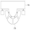
EMI 노이즈는 어느 하나의 전자회로, 소자, 부품 등에서 발생한 전자기파(EM wave)가 다른 회로, 소자, 부품 등으로 전달됨으로써 간섭에 의한 노이즈 문제를 발생시키는 원인이 되는 노이즈를 말한다. 이와 같은 EMI 노이즈를 크게 분류하면, 방사 노이즈(radiation noise, 도 1의 참조번호 10, 30 참조)와 전도 노이즈(conduction noise, 도 1의 참조번호 20 참조)로 나눌 수 있다.EMI noise refers to noise that causes noise problems caused by interference by transmitting an electromagnetic wave generated in one electronic circuit, an element, or a component to another circuit, element, or component. If such EMI noise is largely classified, it can be divided into radiation noise (see
이 중, 기판의 상부(즉, 전자부품의 탑재면)로 방사되는 방사 노이즈(10)의 경우에는 메탈 캡 등의 전자기 차폐용 캡으로 기판 상부 영역을 쉴드(shield)함으로써 해결하는 방식이 일반적이지만, 기판 내부를 통해 흐르는 전도 노이즈(20)가 기판의 가장자리(edge)에까지 전도되어 기판 외부로 방사되는 방사 노이즈(30, 이하 이를 간단히 '에지 노이즈'라 칭함)에 대한 효과적인 해결책에 관한 연구는 아직 미흡한 단계이다.Among these, in the case of the
만일, 기판 구조의 간단한 변경만으로 기판 가장자리에서의 에지 노이즈를 저감할 수 있는 기술이 개발된다면, 메탈 캡이나 회로(circuit) 방식에 의한 해결 방법에 비해 개발 기간 및 비용을 획기적으로 줄일 수 있을 것으로 기대된다. 또한, 공간 활용 측면이나 소비 전력 측면에서도 이점을 가질 수 있으며, 손쉽게 수 GHz 이상의 대역에서도 노이즈를 제거할 수 있게 되어, 기판 에지에서의 EMI 노이즈 문제를 해결하는데 효과적일 것이다.If a technology is developed that can reduce edge noise at the edge of the substrate by simple modification of the substrate structure, it is expected that the development time and cost will be drastically reduced compared to the solution by the metal cap or circuit method. do. In addition, it can have advantages in terms of space utilization and power consumption, and can easily remove noise in a band of several GHz or more, thereby effectively solving the EMI noise problem at the substrate edge.
이에 따라, 본 발명은 특정 주파수 대역의 노이즈를 차폐할 수 있는 전자기 밴드갭 구조를 기판의 가장자리(edge)에 해당하는 기판 내부에 삽입시킴으로써, 기판 가장자리에서 방사되는 방사 노이즈(radiation noise)를 차폐시킬 수 있는 EMI 노이즈 저감 인쇄회로기판을 제공한다.Accordingly, the present invention inserts an electromagnetic bandgap structure that can shield noise of a specific frequency band into the substrate corresponding to the edge of the substrate, thereby shielding radiation noise emitted from the edge of the substrate. To provide EMI noise reduction printed circuit board.
또한, 본 발명은 기판의 간단한 구조 변경만으로 기판 가장자리에서 방사되는 방사 노이즈를 손쉽게 차폐 가능함으로써, 공간 활용도, 제조 비용, 소비 전력 등의 측면에서도 유리한 이점을 갖는 EMI 노이즈 저감 인쇄회로기판을 제공한다.In addition, the present invention provides an EMI noise reduction printed circuit board having advantageous advantages in terms of space utilization, manufacturing cost, power consumption, and the like, by easily shielding radiation noise emitted from the edge of the substrate only by changing the structure of the substrate.
본 발명의 이외의 목적들은 하기의 설명을 통해 쉽게 이해될 수 있을 것이다.Other objects of the present invention will be readily understood through the following description.
본 발명의 일 측면에 따르면, 대역 저지 주파수 특성을 갖는 전자기 밴드갭 구조가 내부에 삽입되는 다층 인쇄회로기판으로서, 그라운드층과 전원층이 마련되는 제1 영역과; 상기 제1 영역의 측면에 위치하여, 상기 제1 영역의 측면을 통해 외부로 방사되는 EMI 노이즈를 차폐하도록 상기 전자기 밴드갭 구조가 마련되는 제2 영역을 포함하되, 상기 전자기 밴드갭 구조는, 상기 제1 영역의 측면을 따라 위치하는 복수 개의 제1 도전판과; 상기 제1 도전판과 다른 평면 상에, 상기 제1 도전판과 교번하도록 배치되는 복수 개의 제2 도전판과; 상기 제1 도전판과 상기 제2 도전판을 연결하는 비아를 포함하는 것을 특징으로 하는 EMI 노이즈 저감 인쇄회로기판이 제공된다.According to an aspect of the present invention, there is provided a multilayer printed circuit board having an electromagnetic bandgap structure having band stop frequency characteristics inserted therein, the first region including a ground layer and a power layer; A second region disposed on a side of the first region and provided with an electromagnetic bandgap structure to shield EMI noise radiated to the outside through the side of the first region, wherein the electromagnetic bandgap structure includes: A plurality of first conductive plates positioned along side surfaces of the first region; A plurality of second conductive plates disposed alternately with the first conductive plate on a plane different from the first conductive plate; An EMI noise reduction printed circuit board is provided, including vias connecting the first conductive plate and the second conductive plate.
상기 제1 영역과 상기 제2 영역은 4층 이상의 다층으로 이루어지고, 상기 비아는 상기 제2 영역의 상하를 관통하는 관통비아일 수 있다.The first region and the second region may be formed of a multilayer of four or more layers, and the via may be a through via penetrating the upper and lower portions of the second region.
또한, 상기 비아는 블라인드 비아일 수도 있다.The via may also be a blind via.
한편, 상기 제1 도전판과 상기 제2 도전판 중 적어도 어느 하나는, 상기 제1 영역의 가장자리 형상에 상응하여 절곡된 형상일 수도 있고, 상기 복수 개의 제1 도전판 중 서로 이웃하는 적어도 어느 한 쌍은, 연결라인에 의해 서로 전기적으로 연결될 수도 있다.Meanwhile, at least one of the first conductive plate and the second conductive plate may be bent to correspond to the edge shape of the first region, and at least one of the plurality of first conductive plates adjacent to each other. The pair may be electrically connected to each other by a connecting line.
상기 제1 도전판은 접속라인에 의해 상기 그라운드층과 전기적으로 연결될 수도 있으며, 상기 제2 영역은 상기 제1 영역의 측면 중 일부에만 선택적으로 배치될 수도 있다.The first conductive plate may be electrically connected to the ground layer by a connection line, and the second region may be selectively disposed only on a part of side surfaces of the first region.
본 발명의 바람직한 실시예에 따르면, 특정 주파수 대역의 노이즈를 차폐할 수 있는 전자기 밴드갭 구조를 기판의 가장자리(edge)에 해당하는 기판 내부에 삽입시킴으로써, 기판 가장자리에서 방사되는 방사 노이즈(radiation noise)를 차폐시킬 수 있는 효과가 있다.According to a preferred embodiment of the present invention, by inserting an electromagnetic bandgap structure capable of shielding noise of a specific frequency band into the substrate corresponding to the edge of the substrate, radiation noise radiated from the edge of the substrate There is an effect that can be shielded.
또한, 기판의 간단한 구조 변경만으로도 기판 가장자리에서 방사되는 방사 노이즈를 손쉽게 차폐 가능함으로써, 공간 활용도, 제조 비용, 소비 전력 등의 측면에서 유리한 효과가 있다.In addition, by simply changing the structure of the substrate can easily shield the radiation noise emitted from the edge of the substrate, there is an advantageous effect in terms of space utilization, manufacturing cost, power consumption.
본 발명은 다양한 변환을 가할 수 있고 여러 가지 실시예를 가질 수 있는 바, 특정 실시예들을 도면에 예시하고 상세한 설명에 상세하게 설명하고자 한다. 그러나, 이는 본 발명을 특정한 실시 형태에 대해 한정하려는 것이 아니며, 본 발명의 사상 및 기술 범위에 포함되는 모든 변환, 균등물 내지 대체물을 포함하는 것으로 이해되어야 한다.As the invention allows for various changes and numerous embodiments, particular embodiments will be illustrated in the drawings and described in detail in the written description. However, this is not intended to limit the present invention to specific embodiments, it should be understood to include all transformations, equivalents, and substitutes included in the spirit and scope of the present invention.
본 발명을 설명함에 있어서, 관련된 공지 기술에 대한 구체적인 설명이 본 발명의 요지를 불필요하게 흐릴 수 있다고 판단되는 경우 그 상세한 설명을 생략한다. 또한, 본 명세서의 설명 과정에서 이용되는 숫자(예를 들어, 제1, 제2 등)는 하나의 구성요소를 다른 구성요소와 구분하기 위한 식별기호에 불과하다.In describing the present invention, when it is determined that the detailed description of the related known technology may unnecessarily obscure the subject matter of the present invention, the detailed description thereof will be omitted. In addition, numerals (eg, first, second, etc.) used in the description process of the present specification are merely identification symbols for distinguishing one component from another component.
본 발명의 EMI 노이즈 저감 인쇄회로기판은 기판 내부의 "전도 노이즈"의 차폐에 목적을 두고 있는 것이 아니라, 그 전도 노이즈가 기판 에지 부분에까지 전도되어 기판 외부로 방사되는 것을 방지(즉, "에지 노이즈"의 차폐)에 목적을 두고 있다. 이를 위해, 본 실시예에 따른 인쇄회로기판은 그라운드층(110)과 전원층(120)이 마련되는 제1 영역(100)과; 상기 제1 영역(100)의 측면에 위치하며 그 내부에 전자기 밴드갭 구조(이하 'EBG 구조'라 한다)가 마련되는 제2 영역(200)을 포함한다. 이 때, EBG 구조는 상기 제1 영역(100)의 측면을 따라 위치하는 복수 개의 제1 도전판(210)과; 상기 제1 도전판(210)과 다른 평면 상에, 상기 제1 도전판(210)과 교번하도록 배치되는 복수 개의 제2 도전판(220)과; 상기 제1 도전판(210)과 상기 제2 도전판(220)을 연결하는 비아(250, 250a)를 포함한다.The EMI noise reduction printed circuit board of the present invention is not aimed at shielding "conduction noise" inside the substrate, but prevents the conducted noise from being conducted to the edge of the substrate and radiated to the outside of the substrate (i.e., "edge noise"). "Screening). To this end, the printed circuit board according to the present embodiment includes a
상기와 같은 도전판들(210, 220)은 그 사이에 개재되는 유전체(미도시)와 더불어서 커패시턴스 성분을 구성하게 되고, 비아(250)는 인덕턴스 성분을 구성하게 된다. 이러한 커패시턴스 성분과 인덕턴스 성분들의 조합에 의해 노이즈를 차폐하는 EBG 구조 즉, L-C 필터가 구성되는 것이다.The
즉, 도 2에 도시된 바와 같이, 본 실시예에 따른 인쇄회로기판은 기판의 에지(edge) 부분에 분리된 도전판들(210, 220, 230, 240)을 형성하고, 이들을 서로 교번되게 구성하여 비아(250)를 통해 연결함으로써, 기판의 에지부분에서 측면으로 방사되는 EMI 노이즈를 차폐하는 구조를 갖는다.That is, as shown in FIG. 2, the printed circuit board according to the present embodiment forms
제1 영역(100)에는 그라운드층(110)과 전원층(120) 등이 마련된다. 도 2에는 최상층에 그라운드층(110)이 마련되고, 그 아래에 전원층(120)이 마련되는 구조가 제시되어 있다. 전원층(120) 아래에 마련되는 두 개의 층(130, 140)은 비아(150)에 의해 그라운드층(110)과 접지되는 구조를 갖는다. 전원층(120)에는 비아(150)와의 전기적인 분리를 위해 클리어런스 홀(125)이 형성된다. 각 층 사이에는 절연체(미도시) 또는 유전체가 개재된다.The
그러나, 상기와 같은 제1 영역(100)의 구성은 일 예에 불과하며, 제1 영역(100)의 구조 및 배치가 다양하게 변경될 수도 있음은 물론이다.However, the configuration of the
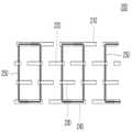
그라운드층(110)과 전원층(120)이 마련된 제1 영역(100)의 측면에 위치하는 제2 영역(200)에는, 본 실시예에 따른 인쇄회로기판의 측면도와 정면도인 도 3 및 도 4에 도시된 바와 같이, 복수의 도전판들(210, 220, 230, 240)이 아래 위가 서로 교번하게 배치된다. 보다 구체적으로, 복수 개의 제1 도전판(210)들이 제1 영역(100)의 측면을 따라 동일 평면 상에 배치되고, 제1 도전판(210)들과 다른 평면 상에 제2 도전판(220)들이 제1 영역(100)의 측면을 따라 배치된다. 이 때, 제2 도 전판(220)들은 제1 도전판(210)들과 서로 교번되도록 배치된다. 즉, 제1 도전판(210)들과 제2 도전판(220)들은 서로의 양 단부가 오버랩 되도록 배치되는 것이다. 이렇게 오버랩 된 제1 도전판(210)과 제2 도전판(220)의 단부는 비아(250)에 의해 서로 연결된다.3 and 4 are side and front views of the printed circuit board according to the present embodiment, in the
여기서 제1 도전판과 제2 도전판은 특정한 기능을 수행하는 도전판을 지칭하는 것이 아니라, 서로 상이한 평면 상에 배치되는 도전판들(210, 220, 230, 240)을 서로 구분하기 위한 것에 지나지 않는다. 또한, 각각의 도전판들(210, 220, 230, 240)은 서로 동일한 크기와 형상을 가질 수도 있으나, 설계 상의 필요 등에 따라 상이한 크기, 상이한 형상을 가질 수도 있다.Here, the first conductive plate and the second conductive plate do not refer to a conductive plate performing a specific function, but merely to distinguish the
또한, 비록 도시되지는 않았으나, 이들 도전판들(210, 220, 230, 240) 사이에는 층간 절연을 위한 절연체 또는 유전체가 개재된다.Also, although not shown, an insulator or dielectric for interlayer insulation is interposed between these
한편, 도 2 내지 도 4에 도시된 바와 같이, 제1 영역(100)과 제2 영역(200)은 4층 이상의 다층으로 이루어질 수 있으며, 이 때, 비아는 제2 영역(200)의 상하를 관통하는 관통비아(250)일 수 있다. 제2 영역(200)이 다층으로 이루어지는 경우, 각 층의 도전판들(210, 220, 230, 240)은 서로 다른 층에 위치하는 도전판과 그 일부가 오버랩 되므로, 오버랩 되는 부분에 관통비아(250)를 형성함으로써, 층간 접속을 보다 간단히 구현할 수 있게 된다. 그 결과, 제조 공정을 매우 단순화 시킬 수 있어, 전반적인 제조비용을 절감할 수 있게 된다.Meanwhile, as shown in FIGS. 2 to 4, the
한편, 도 2 및 도 3에 도시된 바와 같이, 제1 도전판(210)은 접속라인(260)에 의해 제1 영역(100), 보다 구체적으로 그라운드층(110)과 전기적으로 연결될 수 도 있다. 이와 같이 제1 도전판(210)이 그라운드층(110)에 연결되면, 그라운드를 보다 넓게 확보할 수 있어 노이즈 차폐 효과를 보다 더 향상시킬 수 있게 된다.2 and 3, the first
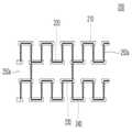
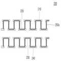
도 5 내지 도 10에는 제2 영역(200)에 삽입되는 EBG 구조의 다양한 변형례들이 도시되어 있다. 도 5에 도시된 바와 같이, 복수 개의 제1 도전판(210) 중 서로 이웃하는 적어도 어느 한 쌍은, 연결라인(215)에 의해 서로 전기적으로 연결될 수 있다. 이렇게 서로 이웃하는 제1 도전판(210)들 사이에 연결라인(215)을 형성하게 되면, 제1 도전판(210) 사이들 사이에 인덕턴스 성분을 추가할 수 있게 되어, 보다 효율적인 노이즈 차폐를 위한 설계 자유도를 향상시킬 수 있는 장점이 있다. 도 5 내지 도 7에 도시된 EBG 구조의 경우에는 제2 영역(200)에 마련되는 모든 도전판들이 관통비아(250)와 연결라인(215)에 의해 제2 영역(200) 내에서 전기적으로 연결되는 구조를 갖는다.5 to 10 illustrate various modifications of the EBG structure inserted into the
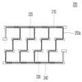
한편, 도 8 내지 도 10에 도시된 EBG 구조의 경우에는, 몇몇 도전판들이 독립된 패스를 형성하고, 이들 각각이 제1 영역(100)의 그라운드층(110)과 적어도 하나이상의 접속라인(260)에 의해 연결된다.Meanwhile, in the EBG structure illustrated in FIGS. 8 to 10, some conductive plates form independent paths, each of which is connected to the
한편, 전술한 실시예들에서는 제2 영역(200)에 마련되는 각각의 도전판들(210, 220, 230, 240)이 제2 영역(200)을 관통하는 관통비아(250)에 의해 전기적으로 연결되는 구조를 제시하였으나, 도 11 내지 도 22에 도시된 바와 같이 블라인드 비아(250a)에 의해 개별적으로 연결될 수도 있다. 도 11(a) 및 도 11(b)에 도시 된 바와 같이, 제1 도전판(210)은 접속라인(260)에 의해 제1 영역(100)의 그라운드층(110)과 연결될 수 있으며, 경우에 따라 도 11(a)에 도시된 바와 같이 다른 도전판 역시 접속라인(260)에 의해 제1 영역(100)에 연결될 수도 있다.Meanwhile, in the above-described embodiments, each of the
도 12 내지 도 16에 도시된 EBG 구조의 경우에는, 제2 영역(200)에 마련되는 모든 도전판들(210, 220, 230, 240)이 블라인드 비아들(250a)과 연결라인(215)에 의해 제2 영역(200) 내에서 전기적으로 연결되는 구조를 갖는다.In the case of the EBG structure shown in FIGS. 12 to 16, all
반면, 도 17 내지 도 22에 도시된 EBG 구조의 경우에는, 몇몇 도전판들이 연결라인(215) 및/또는 블라인드 비아(250a)를 이용하여 독립된 패스를 형성하고, 이들 각각이 제1 영역(100)의 그라운드층(110)과 적어도 하나 이상의 접속라인(260)에 의해 연결된다.On the other hand, in the case of the EBG structure shown in FIGS. 17 to 22, some conductive plates form independent paths using the
한편, 도 23에 도시된 바와 같이 제1 영역(100)의 측면이 사각형의 형상을 갖는 경우에는, 제2 영역(200)의 제1 도전판(210) 및/또는 제2 도전판(220) 역시 직사각형의 형상을 가질 것이나, 도 24와 도 25에 도시된 바와 같이 제1 영역(100)이 사각형 이외의 형상을 갖는 경우에는, 제2 영역(200)의 제1 도전판(210) 및/또는 제2 도전판(220) 역시 이에 상응하여 그 외곽이 절곡된 형상을 가질 수 있다. 즉, 도 24에 도시된 바와 같이, 제1 도전판(210)이 절곡된 형상을 갖거나, 도 25에 도시된 바와 같이 곡면을 가질 수도 있고, 도 26에 도시된 바와 같이 삼각형 형상을 가질 수도 있다.Meanwhile, as illustrated in FIG. 23, when the side surface of the
한편, 내부에 EBG 구조가 삽입되는 제2 영역(200)은 제1 영역(100)의 측면 전체에 걸쳐 배치될 수도 있으나, 특정 부분에만 선택적으로 배치될 수도 있다. 이와 같이 특정 부분에만 제2 영역(200)을 선택적으로 배치함으로써, 사용자가 원하는 부분에 대해서만 선택적으로 노이즈를 차폐할 수 있으며, 비용절감의 효과를 기대할 수 있다.Meanwhile, the
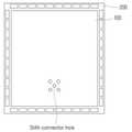
이상에서 제안한 구조에 대하여, EMI 노이즈 차폐효과를 검증하기 위하여 샘플을 제작하여 측정하여 보았다. 도 27은 측정을 위한 샘플의 평면도이고, SMA 커넥터를 장착하여 노이즈를 강제로 인가하여 테스트 하였다. 도 28(a)는 종래기술에 따른 인쇄회로기판의 측정 결과를 나타내는 그래프이고, 도 28(b)는 본 발명의 일 실시예에 따른 인쇄회로기판의 측정 결과를 나타내는 그래프이다.For the proposed structure, samples were fabricated and measured to verify the EMI noise shielding effect. FIG. 27 is a plan view of a sample for measurement and was tested by forcibly applying noise by installing an SMA connector. Figure 28 (a) is a graph showing the measurement result of the printed circuit board according to the prior art, Figure 28 (b) is a graph showing the measurement result of the printed circuit board according to an embodiment of the present invention.
도 28을 통해 확인할 수 있는 바와 같이, 표시된 영역에서 기존 기판은 40dBuV이상(검은색)의 EMI 노이즈가 방사됨을 확인할 수 있으며, 본 발명의 일 실시예에 따른 인쇄회로기판은 34dBuV 이하의 EMI 노이즈가 방사됨을 알 수 있다. 측정 결과에서 알 수 있듯이 제안된 구조를 적용한 기판에서의 EMI 노이즈가 획기적으로 감소함을 확인할 수 있다.As can be seen through FIG. 28, it can be seen that the existing substrate emits 40 dBuV or more (black) EMI noise in the indicated area, and the printed circuit board according to the embodiment of the present invention has EMI noise of 34 dBuV or less. It can be seen that the radiation. As can be seen from the measurement results, it can be seen that the EMI noise on the substrate using the proposed structure is significantly reduced.
상기에서는 본 발명의 바람직한 실시예를 참조하여 설명하였지만, 해당 기술 분야에서 통상의 지식을 가진 자라면 하기의 특허 청구의 범위에 기재된 본 발명의 사상 및 영역으로부터 벗어나지 않는 범위 내에서 본 발명을 다양하게 수정 및 변 경시킬 수 있음을 이해할 수 있을 것이다.Although the above has been described with reference to a preferred embodiment of the present invention, those skilled in the art to which the present invention pertains without departing from the spirit and scope of the present invention as set forth in the claims below It will be appreciated that modifications and changes can be made.
전술한 실시예 외의 많은 실시예들이 본 발명의 특허청구범위 내에 존재한다.Many embodiments other than the above-described embodiments are within the scope of the claims of the present invention.
도 1은 전자소자가 실장된 인쇄회로기판에서 노이즈가 방사되는 모습을 나타내는 도면.1 is a diagram illustrating a state in which noise is radiated from a printed circuit board on which an electronic device is mounted.
도 2는 본 발명의 일 실시예에 따른 EMI 노이즈 저감 인쇄회로기판을 나타내는 사시도.Figure 2 is a perspective view showing an EMI noise reduction printed circuit board according to an embodiment of the present invention.
도 3은 본 발명의 일 실시예에 따른 EMI 노이즈 저감 인쇄회로기판을 나타내는 측면도.Figure 3 is a side view showing an EMI noise reduction printed circuit board according to an embodiment of the present invention.
도 4는 본 발명의 일 실시예에 따른 EMI 노이즈 저감 인쇄회로기판을 나타내는 정면도.Figure 4 is a front view showing an EMI noise reduction printed circuit board according to an embodiment of the present invention.
도 5 내지 도 22는 본 발명의 다양한 실시예에 따른 EMI 노이즈 저감 인쇄회로기판을 나타내는 정면도.5 to 22 are front views illustrating an EMI noise reduction printed circuit board according to various embodiments of the present disclosure.
도 23 내지 도 26은 본 발명의 다양한 실시예에 따른 EMI 노이즈 저감 인쇄회로기판을 나타내는 평면도.23 to 26 are plan views illustrating EMI noise reduction printed circuit boards according to various embodiments of the present disclosure.
도 27은 본 발명의 일 실시예에 따른 EMI 노이즈 저감 인쇄회로기판의 성능 테스트 과정을 나타내는 도면.27 is a view showing a performance test process of the EMI noise reduction printed circuit board according to the embodiment of the present invention.
도 28은 본 발명의 일 실시예에 따른 EMI 노이즈 저감 인쇄회로기판의 성능 테스트 결과를 나타내는 그래프.28 is a graph illustrating performance test results of an EMI noise reduction printed circuit board according to an exemplary embodiment of the present invention.
<도면의 주요부분에 대한 부호의 설명><Description of the symbols for the main parts of the drawings>
100: 제1 영역200: 제2 영역100: first region 200: second region
210: 제1 도전판215: 연결라인210: first conductive plate 215: connection line
220: 제2 도전판250: 관통비아220: second conductive plate 250: through via
260: 접속라인260: connection line
Claims (7)
Translated fromKoreanPriority Applications (4)
| Application Number | Priority Date | Filing Date | Title |
|---|---|---|---|
| KR1020090073444AKR101072591B1 (en) | 2009-08-10 | 2009-08-10 | Electromagnetic interference noise reduction board using electromagnetic bandgap structure |
| US12/654,545US8258408B2 (en) | 2009-08-10 | 2009-12-22 | Electromagnetic interference noise reduction board using electromagnetic bandgap structure |
| JP2009293154AJP5164965B2 (en) | 2009-08-10 | 2009-12-24 | EMI noise reduction printed circuit board |
| TW098146469ATWI454189B (en) | 2009-08-10 | 2009-12-31 | Electromagnetic interference noise reduction board using electromagnetic bandgap structure |
Applications Claiming Priority (1)
| Application Number | Priority Date | Filing Date | Title |
|---|---|---|---|
| KR1020090073444AKR101072591B1 (en) | 2009-08-10 | 2009-08-10 | Electromagnetic interference noise reduction board using electromagnetic bandgap structure |
Publications (2)
| Publication Number | Publication Date |
|---|---|
| KR20110015971A KR20110015971A (en) | 2011-02-17 |
| KR101072591B1true KR101072591B1 (en) | 2011-10-11 |
Family
ID=43533957
Family Applications (1)
| Application Number | Title | Priority Date | Filing Date |
|---|---|---|---|
| KR1020090073444AExpired - Fee RelatedKR101072591B1 (en) | 2009-08-10 | 2009-08-10 | Electromagnetic interference noise reduction board using electromagnetic bandgap structure |
Country Status (4)
| Country | Link |
|---|---|
| US (1) | US8258408B2 (en) |
| JP (1) | JP5164965B2 (en) |
| KR (1) | KR101072591B1 (en) |
| TW (1) | TWI454189B (en) |
Cited By (2)
| Publication number | Priority date | Publication date | Assignee | Title |
|---|---|---|---|---|
| WO2022154294A1 (en)* | 2021-01-12 | 2022-07-21 | 삼성전자 주식회사 | Electronic device including substrates having shielding structure |
| US11848279B2 (en) | 2021-01-12 | 2023-12-19 | Samsung Electronics Co., Ltd. | Electronic device including printed circuit board having shielding structure |
Families Citing this family (14)
| Publication number | Priority date | Publication date | Assignee | Title |
|---|---|---|---|---|
| CN103098567B (en)* | 2010-09-28 | 2015-08-12 | 日本电气株式会社 | Structure and wiring substrate |
| JP6027905B2 (en)* | 2013-01-31 | 2016-11-16 | 新光電気工業株式会社 | Semiconductor device |
| FR3006505B1 (en)* | 2013-05-31 | 2017-02-10 | Commissariat Energie Atomique | DEVICE FOR DISTURBING ELECTROMAGNETIC WAVE PROPAGATION AND METHOD FOR MANUFACTURING THE SAME |
| KR101905507B1 (en) | 2013-09-23 | 2018-10-10 | 삼성전자주식회사 | Antenna device and electronic device with the same |
| JP6278720B2 (en)* | 2014-01-28 | 2018-02-14 | キヤノン株式会社 | Cell and electromagnetic band gap structure |
| JP2015142367A (en) | 2014-01-30 | 2015-08-03 | キヤノン株式会社 | metamaterial |
| US9433090B2 (en) | 2014-03-25 | 2016-08-30 | Microsoft Technology Licensing, Llc | Edge plated printed circuit board |
| JP6414017B2 (en)* | 2015-10-28 | 2018-10-31 | 三菱電機株式会社 | Electromagnetic wave attenuation structure and electromagnetic shield structure |
| US10791622B2 (en)* | 2016-07-27 | 2020-09-29 | National University Corporation Okayama University | Printed wiring board |
| KR20180012981A (en)* | 2016-07-28 | 2018-02-07 | 삼성전자주식회사 | Common board of an adaptor for a tester, adaptor for a tester including the common board and tester including the common board |
| US20180123245A1 (en)* | 2016-10-28 | 2018-05-03 | Broadcom Corporation | Broadband antenna array for wireless communications |
| KR102410197B1 (en)* | 2017-06-13 | 2022-06-17 | 삼성전자주식회사 | Circuit board for reducing transmiting loss and electronic device therewith |
| JP6946776B2 (en) | 2017-06-26 | 2021-10-06 | 株式会社リコー | Circuit board |
| JP7355283B2 (en) | 2021-08-18 | 2023-10-03 | 株式会社村田製作所 | antenna element |
Citations (1)
| Publication number | Priority date | Publication date | Assignee | Title |
|---|---|---|---|---|
| WO2008127196A1 (en)* | 2007-04-12 | 2008-10-23 | Agency For Science, Technology And Research | Composite structure for an electronic circuit |
Family Cites Families (58)
| Publication number | Priority date | Publication date | Assignee | Title |
|---|---|---|---|---|
| JPH0770837B2 (en) | 1992-05-20 | 1995-07-31 | インターナショナル・ビジネス・マシーンズ・コーポレイション | Electronic package substrate and method having multilayer wiring |
| US5475606A (en)* | 1993-03-05 | 1995-12-12 | International Business Machines Corporation | Faraday cage for a printed circuit card |
| JP3684239B2 (en)* | 1995-01-10 | 2005-08-17 | 株式会社 日立製作所 | Low EMI electronic equipment |
| JPH09205290A (en)* | 1996-01-24 | 1997-08-05 | Hitachi Ltd | Circuit board having low EMI structure |
| JPH09246776A (en)* | 1996-03-14 | 1997-09-19 | Oki Electric Ind Co Ltd | Printed wiring board |
| JP2877132B2 (en)* | 1997-03-26 | 1999-03-31 | 日本電気株式会社 | Multilayer printed circuit board and manufacturing method thereof |
| JP3058121B2 (en)* | 1997-05-19 | 2000-07-04 | 日本電気株式会社 | Printed board |
| JP3055136B2 (en)* | 1998-03-16 | 2000-06-26 | 日本電気株式会社 | Printed circuit board |
| US6104258A (en)* | 1998-05-19 | 2000-08-15 | Sun Microsystems, Inc. | System and method for edge termination of parallel conductive planes in an electrical interconnecting apparatus |
| US6215372B1 (en)* | 1999-06-02 | 2001-04-10 | Sun Microsystems, Inc. | Method and apparatus for reducing electrical resonances in power and noise propagation in power distribution circuits employing plane conductors |
| JP3669219B2 (en)* | 1999-08-10 | 2005-07-06 | 日本電気株式会社 | Multilayer printed wiring board |
| JP2001251061A (en)* | 2000-03-02 | 2001-09-14 | Sony Corp | Multilayer printed wiring board |
| US6483481B1 (en)* | 2000-11-14 | 2002-11-19 | Hrl Laboratories, Llc | Textured surface having high electromagnetic impedance in multiple frequency bands |
| US6798666B1 (en)* | 2000-12-29 | 2004-09-28 | Ncr Corporation | Introducing loss in a power bus to reduce EMI and electrical noise |
| US6897831B2 (en)* | 2001-04-30 | 2005-05-24 | Titan Aerospace Electronic Division | Reconfigurable artificial magnetic conductor |
| US6937480B2 (en)* | 2001-05-14 | 2005-08-30 | Fuji Xerox Co., Ltd. | Printed wiring board |
| US6476771B1 (en)* | 2001-06-14 | 2002-11-05 | E-Tenna Corporation | Electrically thin multi-layer bandpass radome |
| US6995733B2 (en)* | 2002-12-24 | 2006-02-07 | Intel Corporation | Frequency selective surface and method of manufacture |
| US6933895B2 (en)* | 2003-02-14 | 2005-08-23 | E-Tenna Corporation | Narrow reactive edge treatments and method for fabrication |
| US7016198B2 (en)* | 2003-04-08 | 2006-03-21 | Lexmark International, Inc. | Printed circuit board having outer power planes |
| US7215007B2 (en)* | 2003-06-09 | 2007-05-08 | Wemtec, Inc. | Circuit and method for suppression of electromagnetic coupling and switching noise in multilayer printed circuit boards |
| US20050104678A1 (en)* | 2003-09-11 | 2005-05-19 | Shahrooz Shahparnia | System and method for noise mitigation in high speed printed circuit boards using electromagnetic bandgap structures |
| US7190315B2 (en)* | 2003-12-18 | 2007-03-13 | Intel Corporation | Frequency selective surface to suppress surface currents |
| CN1890854A (en)* | 2003-12-22 | 2007-01-03 | X2Y艾泰钮埃特有限责任公司 | Internally shielded energy conditioner |
| US6967282B2 (en)* | 2004-03-05 | 2005-11-22 | Raytheon Company | Flip chip MMIC on board performance using periodic electromagnetic bandgap structures |
| US20050205292A1 (en)* | 2004-03-18 | 2005-09-22 | Etenna Corporation. | Circuit and method for broadband switching noise suppression in multilayer printed circuit boards using localized lattice structures |
| JP4273098B2 (en)* | 2004-09-07 | 2009-06-03 | キヤノン株式会社 | Multilayer printed circuit board |
| US7253788B2 (en)* | 2004-09-08 | 2007-08-07 | Georgia Tech Research Corp. | Mixed-signal systems with alternating impedance electromagnetic bandgap (AI-EBG) structures for noise suppression/isolation |
| JP4843611B2 (en)* | 2004-10-01 | 2011-12-21 | デ,ロシェモント,エル.,ピエール | Ceramic antenna module and manufacturing method thereof |
| KR100651358B1 (en)* | 2005-06-22 | 2006-11-29 | 삼성전기주식회사 | Printed circuit board incorporating RF module power stage circuit |
| US7209082B2 (en)* | 2005-06-30 | 2007-04-24 | Intel Corporation | Method and apparatus for a dual band gap wideband interference suppression |
| US7626216B2 (en)* | 2005-10-21 | 2009-12-01 | Mckinzie Iii William E | Systems and methods for electromagnetic noise suppression using hybrid electromagnetic bandgap structures |
| JP4047351B2 (en)* | 2005-12-12 | 2008-02-13 | キヤノン株式会社 | Multilayer printed circuit board |
| US7423608B2 (en)* | 2005-12-20 | 2008-09-09 | Motorola, Inc. | High impedance electromagnetic surface and method |
| JP4689461B2 (en)* | 2005-12-26 | 2011-05-25 | 富士通株式会社 | Printed board |
| JP5082250B2 (en)* | 2006-02-02 | 2012-11-28 | 富士通株式会社 | High frequency circuit board |
| TWI286049B (en)* | 2006-04-04 | 2007-08-21 | Advanced Semiconductor Eng | Circuit substrate |
| WO2008024993A2 (en)* | 2006-08-25 | 2008-02-28 | Rayspan Corporation | Antennas based on metamaterial structures |
| US8159413B2 (en)* | 2006-11-01 | 2012-04-17 | Agency For Science, Technology And Research | Double-stacked EBG structure |
| US7586444B2 (en)* | 2006-12-05 | 2009-09-08 | Delphi Technologies, Inc. | High-frequency electromagnetic bandgap device and method for making same |
| KR100851075B1 (en)* | 2007-04-30 | 2008-08-12 | 삼성전기주식회사 | Electromagnetic Bandgap Structures and Printed Circuit Boards |
| US8169790B2 (en)* | 2007-08-07 | 2012-05-01 | Samsung Electro-Mechanics Co., Ltd. | Electromagnetic bandgap structure and printed circuit board |
| US8310840B2 (en)* | 2007-08-07 | 2012-11-13 | Samsung Electro-Mechanics Co., Ltd. | Electromagnetic bandgap structure and printed circuit board |
| KR100913363B1 (en)* | 2007-09-18 | 2009-08-20 | 삼성전기주식회사 | Electromagnetic Bandgap Structures and Printed Circuit Boards with Multi-vias |
| US8159832B2 (en)* | 2007-09-21 | 2012-04-17 | Nokia Corporation | Electromagnetic band gap structures and method for making same |
| KR101192231B1 (en)* | 2007-11-16 | 2012-10-17 | 홀린워스 펀드, 엘.엘.씨. | Filter design methods and filters based on metamaterial structures |
| TWI375499B (en)* | 2007-11-27 | 2012-10-21 | Asustek Comp Inc | Improvement method for ebg structures and multi-layer board applying the same |
| DE102008045055A1 (en)* | 2007-12-07 | 2009-06-10 | Samsung Electro-Mechanics Co., Ltd., Suwon | Electromagnetic bandgap structure and circuit board |
| US8077000B2 (en)* | 2008-01-21 | 2011-12-13 | Samsung Electro-Mechanics Co., Ltd. | Electromagnetic bandgap structure and printed circuit board |
| KR100969660B1 (en) | 2008-01-24 | 2010-07-14 | 한국과학기술원 | Semiconductor Package Substrate with Double Stacked Electromagnetic Bandgap Structure Around Via Hole |
| TWI397931B (en)* | 2008-02-29 | 2013-06-01 | Ind Tech Res Inst | Capacitor devices |
| US8164006B2 (en)* | 2008-03-19 | 2012-04-24 | Samsung Electro-Mechanics Co., Ltd. | Electromagnetic bandgap structure and printed circuit board |
| TWI345874B (en)* | 2008-05-09 | 2011-07-21 | Advanced Semiconductor Eng | Band pass filter |
| TWI333829B (en)* | 2008-05-22 | 2010-11-21 | Univ Nat Taiwan | Apparatus for silencing electromagnetic noise signal |
| JP5380919B2 (en)* | 2008-06-24 | 2014-01-08 | 日本電気株式会社 | Waveguide structure and printed wiring board |
| KR100956689B1 (en)* | 2008-06-27 | 2010-05-10 | 삼성전기주식회사 | Electromagnetic Bandgap Structures and Printed Circuit Boards |
| KR101046716B1 (en)* | 2008-11-28 | 2011-07-06 | 삼성전기주식회사 | Electromagnetic bandgap structures and circuit boards |
| KR101176800B1 (en)* | 2008-12-23 | 2012-08-27 | 한국전자통신연구원 | Arrangement Structure of Electromagnetic Bandgap for Suppressing the Noise and Improving the Signal Integrity |
- 2009
- 2009-08-10KRKR1020090073444Apatent/KR101072591B1/ennot_activeExpired - Fee Related
- 2009-12-22USUS12/654,545patent/US8258408B2/ennot_activeExpired - Fee Related
- 2009-12-24JPJP2009293154Apatent/JP5164965B2/ennot_activeExpired - Fee Related
- 2009-12-31TWTW098146469Apatent/TWI454189B/ennot_activeIP Right Cessation
Patent Citations (1)
| Publication number | Priority date | Publication date | Assignee | Title |
|---|---|---|---|---|
| WO2008127196A1 (en)* | 2007-04-12 | 2008-10-23 | Agency For Science, Technology And Research | Composite structure for an electronic circuit |
Cited By (2)
| Publication number | Priority date | Publication date | Assignee | Title |
|---|---|---|---|---|
| WO2022154294A1 (en)* | 2021-01-12 | 2022-07-21 | 삼성전자 주식회사 | Electronic device including substrates having shielding structure |
| US11848279B2 (en) | 2021-01-12 | 2023-12-19 | Samsung Electronics Co., Ltd. | Electronic device including printed circuit board having shielding structure |
Also Published As
| Publication number | Publication date |
|---|---|
| TWI454189B (en) | 2014-09-21 |
| JP5164965B2 (en) | 2013-03-21 |
| JP2011040703A (en) | 2011-02-24 |
| US8258408B2 (en) | 2012-09-04 |
| KR20110015971A (en) | 2011-02-17 |
| TW201106813A (en) | 2011-02-16 |
| US20110031007A1 (en) | 2011-02-10 |
Similar Documents
| Publication | Publication Date | Title |
|---|---|---|
| KR101072591B1 (en) | Electromagnetic interference noise reduction board using electromagnetic bandgap structure | |
| KR101023541B1 (en) | EMI noise reduction printed circuit board | |
| US8952265B2 (en) | Electromagnetic interference noise reduction package board | |
| KR101007288B1 (en) | Printed Circuit Boards and Electronics | |
| US8699234B2 (en) | EMI noise shield board including electromagnetic bandgap structure | |
| US20050104678A1 (en) | System and method for noise mitigation in high speed printed circuit boards using electromagnetic bandgap structures | |
| KR101021548B1 (en) | Printed Circuit Board with Electromagnetic Bandgap Structure | |
| KR101038236B1 (en) | printed circuit board having electromagnetic bandgap structure | |
| TWI383736B (en) | Electromagnetic interference noise reduction board using electromagnetic bandgap structure | |
| CN101137282A (en) | Electronic appliance | |
| US8102219B2 (en) | Electromagnetic bandgap structure and printed circuit board | |
| WO2017006552A1 (en) | Printed board | |
| KR101021552B1 (en) | EMI noise reduction printed circuit board | |
| KR101092590B1 (en) | Printed Circuit Board with Electromagnetic Bandgap Structure | |
| US8035036B2 (en) | Complementary mirror image embedded planar resistor architecture | |
| KR101021551B1 (en) | Printed Circuit Board with Electromagnetic Bandgap Structure | |
| CN103904063A (en) | Package substrate with band stop filter and semiconductor package including the same | |
| Karuppiah et al. | Compact EBG structure for ground bounce noise suppression in high-speed digital systems. |
Legal Events
| Date | Code | Title | Description |
|---|---|---|---|
| A201 | Request for examination | ||
| PA0109 | Patent application | St.27 status event code:A-0-1-A10-A12-nap-PA0109 | |
| PA0201 | Request for examination | St.27 status event code:A-1-2-D10-D11-exm-PA0201 | |
| D13-X000 | Search requested | St.27 status event code:A-1-2-D10-D13-srh-X000 | |
| D14-X000 | Search report completed | St.27 status event code:A-1-2-D10-D14-srh-X000 | |
| E902 | Notification of reason for refusal | ||
| PE0902 | Notice of grounds for rejection | St.27 status event code:A-1-2-D10-D21-exm-PE0902 | |
| PG1501 | Laying open of application | St.27 status event code:A-1-1-Q10-Q12-nap-PG1501 | |
| P11-X000 | Amendment of application requested | St.27 status event code:A-2-2-P10-P11-nap-X000 | |
| P13-X000 | Application amended | St.27 status event code:A-2-2-P10-P13-nap-X000 | |
| E701 | Decision to grant or registration of patent right | ||
| PE0701 | Decision of registration | St.27 status event code:A-1-2-D10-D22-exm-PE0701 | |
| GRNT | Written decision to grant | ||
| PR0701 | Registration of establishment | St.27 status event code:A-2-4-F10-F11-exm-PR0701 | |
| PR1002 | Payment of registration fee | St.27 status event code:A-2-2-U10-U11-oth-PR1002 Fee payment year number:1 | |
| PG1601 | Publication of registration | St.27 status event code:A-4-4-Q10-Q13-nap-PG1601 | |
| R18-X000 | Changes to party contact information recorded | St.27 status event code:A-5-5-R10-R18-oth-X000 | |
| FPAY | Annual fee payment | Payment date:20141001 Year of fee payment:4 | |
| PR1001 | Payment of annual fee | St.27 status event code:A-4-4-U10-U11-oth-PR1001 Fee payment year number:4 | |
| FPAY | Annual fee payment | Payment date:20150930 Year of fee payment:5 | |
| PR1001 | Payment of annual fee | St.27 status event code:A-4-4-U10-U11-oth-PR1001 Fee payment year number:5 | |
| FPAY | Annual fee payment | Payment date:20161004 Year of fee payment:6 | |
| PR1001 | Payment of annual fee | St.27 status event code:A-4-4-U10-U11-oth-PR1001 Fee payment year number:6 | |
| FPAY | Annual fee payment | Payment date:20171011 Year of fee payment:7 | |
| PR1001 | Payment of annual fee | St.27 status event code:A-4-4-U10-U11-oth-PR1001 Fee payment year number:7 | |
| FPAY | Annual fee payment | Payment date:20181001 Year of fee payment:8 | |
| PR1001 | Payment of annual fee | St.27 status event code:A-4-4-U10-U11-oth-PR1001 Fee payment year number:8 | |
| R18-X000 | Changes to party contact information recorded | St.27 status event code:A-5-5-R10-R18-oth-X000 | |
| FPAY | Annual fee payment | Payment date:20191001 Year of fee payment:9 | |
| PR1001 | Payment of annual fee | St.27 status event code:A-4-4-U10-U11-oth-PR1001 Fee payment year number:9 | |
| PR1001 | Payment of annual fee | St.27 status event code:A-4-4-U10-U11-oth-PR1001 Fee payment year number:10 | |
| PR1001 | Payment of annual fee | St.27 status event code:A-4-4-U10-U11-oth-PR1001 Fee payment year number:11 | |
| PR1001 | Payment of annual fee | St.27 status event code:A-4-4-U10-U11-oth-PR1001 Fee payment year number:12 | |
| PC1903 | Unpaid annual fee | St.27 status event code:A-4-4-U10-U13-oth-PC1903 Not in force date:20231006 Payment event data comment text:Termination Category : DEFAULT_OF_REGISTRATION_FEE | |
| PC1903 | Unpaid annual fee | St.27 status event code:N-4-6-H10-H13-oth-PC1903 Ip right cessation event data comment text:Termination Category : DEFAULT_OF_REGISTRATION_FEE Not in force date:20231006 |