KR101070583B1 - Optical structure for fingerprint acquisition - Google Patents
Optical structure for fingerprint acquisitionDownload PDFInfo
- Publication number
- KR101070583B1 KR101070583B1KR1020100126479AKR20100126479AKR101070583B1KR 101070583 B1KR101070583 B1KR 101070583B1KR 1020100126479 AKR1020100126479 AKR 1020100126479AKR 20100126479 AKR20100126479 AKR 20100126479AKR 101070583 B1KR101070583 B1KR 101070583B1
- Authority
- KR
- South Korea
- Prior art keywords
- fingerprint
- image
- prism
- input surface
- unit
- Prior art date
- Legal status (The legal status is an assumption and is not a legal conclusion. Google has not performed a legal analysis and makes no representation as to the accuracy of the status listed.)
- Active
Links
Images


Classifications
- G—PHYSICS
- G02—OPTICS
- G02B—OPTICAL ELEMENTS, SYSTEMS OR APPARATUS
- G02B17/00—Systems with reflecting surfaces, with or without refracting elements
- G02B17/08—Catadioptric systems
- G—PHYSICS
- G02—OPTICS
- G02B—OPTICAL ELEMENTS, SYSTEMS OR APPARATUS
- G02B5/00—Optical elements other than lenses
- G02B5/04—Prisms
- G—PHYSICS
- G06—COMPUTING OR CALCULATING; COUNTING
- G06V—IMAGE OR VIDEO RECOGNITION OR UNDERSTANDING
- G06V40/00—Recognition of biometric, human-related or animal-related patterns in image or video data
- G06V40/10—Human or animal bodies, e.g. vehicle occupants or pedestrians; Body parts, e.g. hands
- G06V40/12—Fingerprints or palmprints
- G06V40/13—Sensors therefor
- G06V40/1324—Sensors therefor by using geometrical optics, e.g. using prisms
Landscapes
- Physics & Mathematics (AREA)
- General Physics & Mathematics (AREA)
- Optics & Photonics (AREA)
- Engineering & Computer Science (AREA)
- Human Computer Interaction (AREA)
- Multimedia (AREA)
- Theoretical Computer Science (AREA)
- Image Input (AREA)
Abstract
Translated fromKoreanDescription
Translated fromKorean본 발명은 지문획득을 위한 광학구조에 관한 것으로, 보다 상세하게는 광학식 지문인식과정에서 고해상도이면서 왜곡을 최소화한 지문영상을 획득할 수 있도록 하는 지문획득을 위한 광학구조에 관한 것이다.The present invention relates to an optical structure for fingerprint acquisition, and more particularly, to an optical structure for fingerprint acquisition to obtain a fingerprint image with high resolution and minimized distortion in an optical fingerprint recognition process.
일반적으로, 지문인식을 통한 사용자 인증은 사용이 편리할 뿐만 아니라, 보안성 및 경제성이 뛰어나 현재 많이 상용화되어 있다. 기존의 광학식 지문획득장비는 지문을 획득하기 위해 프리즘을 사용한다. 즉, 프리즘의 내부전반사 특성을 이용하여 제작되는 광학식 지문광학계는 별도의 왜곡 보상 기술을 적용하지 않을 경우 광학적 특성에 의해 렌즈를 통과하여 촬영된 영상에 사다리꼴 왜곡현상이 포함되게 된다.In general, user authentication through fingerprint recognition is not only convenient to use, but also excellent in security and economy, and is currently widely commercialized. Conventional optical fingerprint acquisition equipment uses a prism to acquire a fingerprint. In other words, the optical fingerprint optical system manufactured by using the internal reflection characteristics of the prism includes a trapezoidal distortion phenomenon in the image photographed through the lens due to the optical characteristics unless a separate distortion compensation technique is applied.
따라서, 이러한 광학적 왜곡현상을 보정하여 보다 왜곡이 적은 영상을 얻기 위한 다양한 방법들이 고안되었다.Therefore, various methods have been devised to correct the optical distortion and obtain an image with less distortion.
종래 제시된 지문영상의 왜곡을 보정하는 방법에는 이미지센서를 기울이는 방법, 프리즘과 이미지센서 사이에 광학왜곡 보정용 광학 유닛을 추가하는 방법, 소프트웨어로 보정하는 방법 등이 있다.Conventionally proposed methods for correcting distortion of a fingerprint image include tilting an image sensor, adding an optical unit for correcting optical distortion between the prism and the image sensor, and correcting by software.
그러나, 상기 센서를 기울이는 방법은 정밀한 왜곡 보정이 이루어지지 못하고, 광학보정 유닛을 추가하는 방법은 비용이 너무 많이 들거나 저가의 광학요소를 사용하는 경우 광학적 성능(MTF 등)이 나빠지는 문제점이 있으며, 소프트웨어로 전체 왜곡을 보정하는 방법은 연산의 복잡성으로 인해 왜곡이 보정된 영상을 생성하는데 시간이 많이 걸리는 문제점이 있다.However, the method of tilting the sensor is not accurate distortion correction, the method of adding the optical correction unit has a problem that the optical performance (MTF, etc.) worsens when the cost is too expensive or when using an inexpensive optical element, The method of correcting the total distortion by software has a problem in that it takes a long time to generate the image whose distortion is corrected due to the complexity of the calculation.
상기와 같은 종래 문제점을 해결하기 위한 본 발명에서는 광학적 성능을 저하시키지 않은 범위내에서 최소왜곡을 갖도록 광학계를 구성하고 최종적으로 간단한 소프트웨어 처리 알고리즘을 이용하여 영상의 배율을 조정할 수 있도록 하는 지문획득을 위한 광학구조를 제공하는 데 그 목적이 있다.In the present invention for solving the conventional problems as described above for configuring the optical system to have a minimum distortion within a range that does not degrade the optical performance and finally for a fingerprint acquisition to adjust the magnification of the image using a simple software processing algorithm The purpose is to provide an optical structure.
상기와 같은 목적을 달성하기 위한 본 발명은 빔을 조사받는 입력면과, 수평방향으로 형성되어 손가락이 접촉되는 접촉면과, 상기 입력면으로 조사된 빔이 접촉면의 손가락에서 반사되어 빠져나가는 출력면을 포함하는 프리즘과, 상기 프리즘의 입력면으로 빔을 조사하는 조명부와, 상기 프리즘의 출력면으로 반사된 지문 영상을 반사시키는 반사부와, 상기 반사부를 통해 반사된 지문 영상을 입력받는 2개 이상의 렌즈를 포함하는 렌즈유닛 및 상기 렌즈유닛을 통과한 지문 영상이 결상되는 이미지 센서를 포함하는 지문획득을 위한 광학구조를 제공한다.The present invention for achieving the above object is an input surface to which the beam is irradiated, the contact surface is formed in the horizontal direction to contact the finger, and the output surface from which the beam irradiated to the input surface is reflected off the finger of the contact surface At least two lenses for receiving a prism, an illumination unit for irradiating a beam to an input surface of the prism, a reflector for reflecting a fingerprint image reflected to an output surface of the prism, and a fingerprint image reflected through the reflector It provides an optical structure for obtaining a fingerprint comprising a lens unit comprising an image sensor and an image sensor is imaged through the lens unit.
상기와 같은 본 발명에 따르면, 광학적 성능을 저하시키지 않은 범위내에서 최소왜곡을 갖도록 광학계를 구성하고 최종적으로 간단한 소프트웨어 처리 알고리즘을 이용하여 영상의 배율을 조정할 수 있어 보다 선명하고 정확한 지문영상을 획득할 수 있는 매우 유용한 효과가 있다.According to the present invention as described above, it is possible to configure the optical system to have the minimum distortion within a range that does not degrade the optical performance, and finally to adjust the magnification of the image using a simple software processing algorithm to obtain a clearer and more accurate fingerprint image It has a very useful effect.
또한, 반사부의 작용으로 프리즘에서 출력된 빛의 경로를 굴절시킴으로써 전체 광학계 크기를 축소시켜 결과적으로 제품의 크기를 소형화할 수 있는 유용한 효과가 있다.In addition, there is a useful effect that the size of the product can be reduced by reducing the size of the entire optical system by refracting the path of the light output from the prism by the action of the reflector.
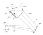
도 1은 본 발명의 일 실시 예에 따른 지문획득을 위한 광학구조의 구성도,
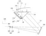
도 2는 본 발명의 다른 실시 예에 따른 지문획득을 위한 광학구조의 구성도,
도 3은 본 발명의 또 다른 실시 예에 따른 지문획득을 위한 광학구조의 구성도,
도 4는 본 발명 지문획득을 위한 광학구조의 부분 확대도.1 is a block diagram of an optical structure for obtaining a fingerprint according to an embodiment of the present invention;
2 is a block diagram of an optical structure for fingerprint acquisition according to another embodiment of the present invention;
3 is a block diagram of an optical structure for fingerprint acquisition according to another embodiment of the present invention;
4 is a partially enlarged view of an optical structure for fingerprint acquisition according to the present invention;
이하, 첨부된 도면에 따라 본 발명 지문획득을 위한 광학구조의 구성 및 작용을 더욱 상세히 설명하면 다음과 같다.Hereinafter, the configuration and operation of the optical structure for fingerprint acquisition according to the present invention according to the accompanying drawings in more detail.
도 1은 본 발명의 일 실시 예에 따른 지문획득을 위한 광학구조의 구성도이고, 도 2는 본 발명의 다른 실시 예에 따른 지문획득을 위한 광학구조의 구성도이며, 도 3은 본 발명의 또 다른 실시 예에 따른 지문획득을 위한 광학구조의 구성도이고, 도 4는 본 발명 지문획득을 위한 광학구조의 부분 확대도이다.1 is a block diagram of an optical structure for fingerprint acquisition according to an embodiment of the present invention, Figure 2 is a block diagram of an optical structure for fingerprint acquisition according to another embodiment of the present invention, Figure 3 is a view of the present invention 4 is a block diagram of an optical structure for fingerprint acquisition according to another embodiment, and FIG. 4 is a partially enlarged view of an optical structure for fingerprint acquisition according to the present invention.
상기 도 1 내지 도 3에 도시한 바와 같이 본 발명에 따른 지문획득을 위한 광학구조는 프리즘(100), 조명부(200), 반사부(300), 렌즈유닛(400), 이미지센서(500)를 포함한다.As shown in FIGS. 1 to 3, the optical structure for fingerprint acquisition according to the present invention includes a
먼저, 상기 프리즘(100)은 빔(B)을 조사받는 입력면(110)과, 수평방향으로 형성되어 손가락(F)이 접촉되는 접촉면(120)과, 상기 입력면(110)으로 조사된 빔(B)이 접촉면(120)의 손가락(F)에서 반사되어 빠져나가는 출력면(130)을 포함한다.First, the
조명부(200)는 상기 프리즘(100)의 입력면(110)으로 빔(B)을 조사하는 구성으로, 상기 조명부(200)는 프리즘(100)의 광학적 평면들 중 입력면(110)을 향해 빛을 조사하도록 배치될 수 있다. 이에 따라, 상기 조명부(200)로부터 조사된 빛은 프리즘(100)의 접촉면(120), 즉 접촉면(120)에 접촉된 손가락의 지문에서 반사되어 출력면(130)으로 빠져나간 뒤, 반사부(300)로 진행할 수 있다.The
상기 조명부(200)는 공지의 다양한 발광수단이 적용될 수 있으며, 특히 다수의 LED 등이 배열된 구성으로 이루어질 수 있으며, 바람직하게는 입력면(110)에 전면적으로 빛을 조사하는 라인빔 또는 면조명의 형태를 취한다..The
반사부(300)는 상기 프리즘(100)의 출력면(130)으로 반사된 지문 영상(FP)을 반사시키는 작용을 한다.The
본 발명의 바람직한 실시 예에 따르면, 상기 반사부(300)는 입력된 지문 영상(FP)을 렌즈유닛(400)으로 집중 반사시키는 오목거울로 마련된다.According to a preferred embodiment of the present invention, the
상기 반사부(300)는 지문 영상(FP)의 경로를 전환시켜주기도 하지만, 광학 오목거울로 구비된 경우, 지문 영상(FP)의 기하학적 왜곡을 보상해주기도 한다.The
상기와 같이 프리즘(100)과 렌즈군(400) 사이에 위치한 광학오목거울로 구비된 반사부(300)에서 1차로 대형 사다리꼴 왜곡을 보상해주면, 상기 중심축이 서로 엇가리도록 배치된 렌즈(410, 420)들과 센서의 기울임을 통해 왜곡이 보다 정밀하게 보상된다.As described above, when the large trapezoidal distortion is first compensated for in the
렌즈유닛(400)은 상기 반사부(300)를 통해 반사된 지문 영상(FP)을 입력받는 2개 이상의 렌즈(410,420)를 포함한다.The
상기 렌즈유닛(400)은 반사부(300)에 의해 반사된 지문 영상(FP)을 받아서 광학적 상을 맺도록 작용한다. 한편, 상기 렌즈유닛(400)은 프리즘(100)의 출력면(130)으로 출력된 빛이 상기 반사부(300)를 거치지 않고 곧바로 받을 수 있도록 배치될 수 있다.The
이미지센서(500)는 상기 렌즈유닛(400)을 통과한 지문 영상(FP)이 결상되도록 마련된다.The
상기 이미지센서(500)는 렌즈유닛(400)을 통해 맺힌 광학적 상을 전기적 신호로 변환하고 영상 처리한다. 이미지센서(500)는 영상 처리부와 전기적으로 연결될 수 있다. 이미지센서(500)는 광학적 상을 전기신호로 변환하는 것으로, CCD 또는 CMOS 등의 이미지 센서로 이루어질 수 있다.The
영상 처리부는 이미지센서(500)에 의해 변환된 전기신호를 영상 처리하여 획득할 수 있다. 이렇게 획득된 지문 영상은 지문인식 알고리즘에 의해 등록된 지문 영상과 비교되어 등록된 지문인지 여부를 판단하는 정보로 이용될 수 있다.
The image processor may acquire an image by processing the electrical signal converted by the
참고로, 본 발명 지문획득을 위한 광학구조에서는 프리즘(100), 조명부(200), 렌즈유닛(400), 이미지 센서(500)를 포함하지만, 광학적 성능 향상을 위해 광 BPF(band-pass filter)를 추가하거나 광학 거울 등을 사용하여 광로를 굴절시킴으로써 전체 광학계 크기를 축소시켜 결과적으로 제품의 크기를 소형화할 수 있다.For reference, the optical structure for acquiring the fingerprint of the present invention includes a
또한, 고해상도, 저왜곡 영상을 얻기 위해 렌즈의 매수를 늘리거나 비구면 렌즈를 사용하여 각종 광학 왜곡 요인들을 줄일 수도 있다.
In addition, various optical distortion factors may be reduced by increasing the number of lenses or using an aspherical lens to obtain a high resolution and low distortion image.
본 발명의 바람직한 실시 예에 따르면, 상기 렌즈유닛(400)은 제1렌즈(410)와 제2렌즈(420)를 포함한다.According to a preferred embodiment of the present invention, the
제1렌즈(410)는 상기 반사부(300)를 통해 반사된 지문 영상(FP)을 입력받도록 전방에 배치되고, 제2렌즈(420)는 상기 제1렌즈(410)와 상호 중심축이 어긋나도록 후방에 배치되고, 상기 제1렌즈(410)를 통과한 지문 영상(FP)을 입력받는다.The
일례로, 상기 반사부(300)를 통해서 반사된 지문영상(FP)이 제1렌즈(410)의 중심축을 기준으로 상부와 하부에 균일하게 조사되어 통과한다.For example, the fingerprint image FP reflected through the
상기 제1렌즈(410)를 통과한 지문영상(FP)의 일측 단부가 제2렌즈(420)의 중심축을 통과하도록 배치될 수 있다.One end of the fingerprint image FP passing through the
최종적으로, 제2렌즈(420)를 통과한 지문영상(FP)은 이미지센서(500)에 결상된다.
Finally, the fingerprint image FP passing through the
본 발명의 바람직한 실시 예에 따르면, 본 발명 지문획득을 위한 광학구조는 영상조정부(600)를 더 포함한다.According to a preferred embodiment of the present invention, the optical structure for obtaining a fingerprint of the present invention further includes an
영상조정부(600)는 상기 지문이 입력되는 접촉면(120)과 종횡비 또는 크기가 동일하도록 상기 이미지센서(500)로 결상된 지문영상(FP)을 조정하도록 마련된다.The
예를 들어, 본 발명의 광학적 특성으로 인하여 프리즘(100)의 접촉면(120)을 통해 입력된 지문 채취영상이 정사각형이라고 가정했을 때, 프리즘(100)과 렌즈유닛(400)을 통과하여 이미지센서(500)에 결상될 때 그 형상이 정사각형이 아니며, 및 기존의 광학구조에서 결상되었던 사다리꼴도 아닌 가로(또는 세로)로 길다란 직사각형 형태를 취하게 된다.For example, when it is assumed that the fingerprint image input through the
즉, 최종적으로 촬영된 영상은 종축(또는 횡축) 방향에 대해서는 광학 배율 변화가 발생하지 않으나 횡축(또는 종축) 방향은 목표로 하는 배율보다 높게 영상이 취득된다. 따라서, 종횡비가 동일하도록 종축 또는 횡축을 기준으로 영상을 조절할 필요가 있다.That is, in the finally captured image, the optical magnification change does not occur in the vertical axis (or horizontal axis) direction, but the image is acquired in the horizontal axis (or vertical axis) direction higher than the target magnification. Therefore, it is necessary to adjust the image based on the vertical axis or the horizontal axis so that the aspect ratio is the same.
예를 들어, 500DPI를 목표로 하는 지문채취장비에서 종축 방향은 500DPI로 횡축방향은 500DPI 이상으로 영상이 취득될 수 있다.For example, an image may be acquired with a vertical axis direction of 500DPI and a horizontal axis direction of 500DPI or more in a fingerprint device targeting 500 DPI.
상기와 같이 획득된 영상은 가로로 긴 직사각형 형태를 갖기 때문에 단순 소프트웨어 알고리즘과 같은 영상조정부(600)를 사용하여 고속으로 횡방향 배율을 조정한다.Since the image obtained as described above has a horizontally long rectangular shape, the horizontal magnification is adjusted at high speed using an
반대로, 반사부(300) 및 렌즈유닛(400)의 정렬구조에 따라 500DPI를 목표로 하는 지문채취장비에서 횡축 방향은 500DPI로 종축방향은 500DPI 이상으로 영상이 취득될 수 있다.On the contrary, according to the alignment structure of the
상기의 경우에도 획득된 영상은 세로로 긴 직사각형 형태를 갖기 때문에 단순 소프트웨어 알고리즘과 같은 영상조정부(600)를 사용하여 고속으로 종방향 배율 을 조정하여 회전지문 또는 연속 지문 촬영시 왜곡이 없는 영상을 실시간으로 처리할 수 있도록 한다.
Even in the above case, since the acquired image has a vertically long rectangular shape, the
본 발명의 바람직한 실시 예에 따르면, 상기 프리즘(100)의 입력면(110)은 상기 접촉면(120)과 이웃하며 접촉면(120)과 하향 경사지도록 형성된 제1입력면(111)을 포함하고, 상기 조명부(200)는 상기 제1입력면(111)에 빔(B)을 조사하는 제1조명부(210)를 포함한다.According to a preferred embodiment of the present invention, the
상기 입력면(110)과 조명부(200)가 제1입력면(111) 및 제1조명부(210)와 같은 구조를 취함에 따라 제1조명부(210)에서 조사된 빔(B)은 프리즘(100)내에서 전반사가 이루어져 흡수식 지문채취 광학계에 적용될 수 있다.
As the
본 발명의 바람직한 실시 예에 따르면,상기 프리즘(100)의 입력면(110)은 상기 접촉면(120)의 맞은편에 접촉면(120)과 평행하도록 형성된 제2입력면(112)을 포함하고, 상기 조명부(200)는 상기 제2입력면(112)에 빔(B')을 조사하는 제2조명부(220)를 포함한다.According to a preferred embodiment of the present invention, the
상기 입력면(110)과 조명부(200)가 제2입력면(112) 및 제2조명부(220)와 같은 구조를 취함에 따라 제2조명부(220)에서 조사된 빔(B')은 전반사가 이루어지지 않기 때문에 산란식 지문채취 광학계에 적용될 수 있다.
As the
상기한 바와 같은 광학구조의 성능을 유지하기 위해서는 프리즘(100)과 반사부(300)의 거리와 정렬 정도가 중요하며 이미지 센서(500) 앞단에 위치한 렌즈(110, 120)들의 개별 광축 정렬 정도 또한 매우 중요하다. 일정 수준의 성능을 얻기 위해서는 프리즘(100)과 반사부(300) 및 렌즈유닛(400)의 정렬에 주의를 기울여야 한다.In order to maintain the performance of the optical structure as described above, the distance and the degree of alignment between the
상기와 같은 본 발명은 광학적 성능을 저하시키지 않은 범위내에서 최소왜곡을 갖도록 광학계를 구성하고 최종적으로 영상조정부(600)를 통해 영상의 배율을 조정할 수 있어 보다 선명하고 정확한 지문영상을 획득할 수 있으며, 상기 반사부(300)의 작용으로 프리즘(100)에서 출력된 빛의 경로를 굴절시킴으로써 전체 광학계 크기를 축소시켜 결과적으로 제품의 크기를 소형화할 수 있는 장점이 있다.In the present invention as described above, the optical system may be configured to have minimum distortion within a range that does not deteriorate optical performance, and finally, the
본 발명 지문인식을 위한 광학구조는 첨부된 도면에 도시된 일 실시 예를 참고로 설명되었으나 이는 예시적인 것에 불과하며, 당해 기술분야에서 통상의 지식을 가진 자라면 이로부터 다양한 변형 및 균등한 타 실시예가 가능하다는 점을 이해할 수 있을 것이다. 따라서, 본 발명의 진정한 보호 범위는 첨부된 청구 범위에 의해서만 정해져야 할 것이다.The optical structure for fingerprint recognition of the present invention has been described with reference to one embodiment shown in the accompanying drawings, but this is merely exemplary, and those skilled in the art may various modifications and other equivalent implementations therefrom. It will be appreciated that examples are possible. Accordingly, the true scope of protection of the present invention should be determined only by the appended claims.
B, B' : 빔 F : 손가락
FP : 지문 영상 100 : 프리즘
110 : 입력면 120 : 접촉면
130 : 출력면 140 : 보조입력면
200 : 조명부 210 : 보조조명부
300 : 반사부 400 : 렌즈유닛
410 : 제1렌즈 420 : 제2렌즈
500 : 이미지센서 600 : 영상조정부B, B ': beam F: finger
FP: fingerprint image 100: prism
110: input surface 120: contact surface
130: output surface 140: auxiliary input surface
200: lighting unit 210: auxiliary lighting unit
300: reflection unit 400: lens unit
410: first lens 420: second lens
500: image sensor 600: image control unit
Claims (6)
Translated fromKorean빔을 조사받는 입력면과, 수평방향으로 형성되어 손가락이 접촉되는 접촉면과, 상기 입력면으로 조사된 빔이 접촉면의 손가락에서 반사되어 빠져나가는 출력면을 포함하는 프리즘과;
상기 프리즘의 입력면으로 빔을 조사하는 조명부;
상기 프리즘의 출력면으로 빠져나온 지문 영상을 입력받아 집중반사시키는 오목거울 형태의 반사부;
상기 반사부를 통해 반사된 지문 영상을 입력받도록 전방에 배치되는 제1렌즈와, 상기 제1렌즈와 상호 중심축이 어긋나도록 후방에 배치되고, 상기 제1렌즈를 통과한 지문 영상을 입력받는 제2렌즈로 이루어진 렌즈유닛; 및
상기 렌즈유닛을 통과한 지문 영상이 결상되는 이미지 센서;를 포함하는 것을 특징으로 하는 지문획득을 위한 광학구조.In the optical structure for fingerprint acquisition,
A prism including an input surface to which the beam is irradiated, a contact surface formed in a horizontal direction to which a finger contacts, and an output surface to which the beam irradiated to the input surface is reflected from the finger of the contact surface and exits;
An illumination unit irradiating a beam to an input surface of the prism;
A concave mirror-shaped reflector configured to receive and receive a fingerprint image exiting the output surface of the prism;
A first lens disposed in front to receive the fingerprint image reflected through the reflecting unit; A lens unit made of a lens; And
And an image sensor for forming a fingerprint image passing through the lens unit.
상기 지문이 입력되는 접촉면과 종횡비 또는 크기가 동일하도록 상기 이미지센서로 결상된 지문영상을 조정하는 영상조정부;를 더 포함하는 것을 특징으로 하는 지문획득을 위한 광학구조.The method of claim 1,
And an image adjusting unit configured to adjust the fingerprint image formed by the image sensor so that the aspect ratio or the size of the contact surface to which the fingerprint is input is the same.
상기 프리즘의 입력면은 상기 접촉면과 이웃하며 접촉면과 경사지도록 형성된 제1입력면을 포함하고,
상기 조명부는 상기 제1입력면에 빔을 조사하는 제1조명부를 포함하는 것을 특징으로 하는 지문획득을 위한 광학구조.The method of claim 1,
The input surface of the prism includes a first input surface adjacent to the contact surface and formed to be inclined with the contact surface,
The illumination unit includes a first lighting unit for irradiating a beam to the first input surface, the optical structure for fingerprint acquisition.
상기 프리즘의 입력면은 상기 접촉면의 맞은편에 접촉면과 평행하도록 형성된 제2입력면을 포함하고,
상기 조명부는 상기 제2입력면에 빔을 조사하는 제2조명부를 포함하는 것을 특징으로 하는 지문획득을 위한 광학구조.The method according to claim 1,
The input surface of the prism includes a second input surface formed to be parallel to the contact surface opposite the contact surface,
The illumination unit includes a second illumination unit for irradiating a beam to the second input surface, the optical structure for fingerprint acquisition.
Priority Applications (2)
| Application Number | Priority Date | Filing Date | Title |
|---|---|---|---|
| KR1020100126479AKR101070583B1 (en) | 2010-12-10 | 2010-12-10 | Optical structure for fingerprint acquisition |
| US13/198,013US9223121B2 (en) | 2010-12-10 | 2011-08-04 | Optical structure for acquiring fingerprint image |
Applications Claiming Priority (1)
| Application Number | Priority Date | Filing Date | Title |
|---|---|---|---|
| KR1020100126479AKR101070583B1 (en) | 2010-12-10 | 2010-12-10 | Optical structure for fingerprint acquisition |
Publications (1)
| Publication Number | Publication Date |
|---|---|
| KR101070583B1true KR101070583B1 (en) | 2011-10-06 |
Family
ID=45032378
Family Applications (1)
| Application Number | Title | Priority Date | Filing Date |
|---|---|---|---|
| KR1020100126479AActiveKR101070583B1 (en) | 2010-12-10 | 2010-12-10 | Optical structure for fingerprint acquisition |
Country Status (2)
| Country | Link |
|---|---|
| US (1) | US9223121B2 (en) |
| KR (1) | KR101070583B1 (en) |
Cited By (1)
| Publication number | Priority date | Publication date | Assignee | Title |
|---|---|---|---|---|
| KR20190063730A (en)* | 2017-11-30 | 2019-06-10 | 삼성전자주식회사 | Wearable electronic device having a fingerprint sensor |
Families Citing this family (5)
| Publication number | Priority date | Publication date | Assignee | Title |
|---|---|---|---|---|
| JP5633054B2 (en)* | 2010-10-29 | 2014-12-03 | 株式会社オプトロジック | Imaging device |
| US9330294B2 (en) | 2012-01-26 | 2016-05-03 | Aware, Inc. | System and method of capturing and producing biometric-matching quality fingerprints and other types of dactylographic images with a mobile device |
| KR101441331B1 (en)* | 2013-07-19 | 2014-09-17 | 주식회사 슈프리마 | Optical type fingerprint recognition apparatus |
| KR20190088822A (en)* | 2018-01-19 | 2019-07-29 | 삼성전자주식회사 | Sensor and electronic apparatus for fingerprint recognition |
| US20200409191A1 (en)* | 2019-06-28 | 2020-12-31 | Shenzhen GOODIX Technology Co., Ltd. | Enhancement film for under-screen optical fingerprint sensor |
Citations (1)
| Publication number | Priority date | Publication date | Assignee | Title |
|---|---|---|---|---|
| KR100726100B1 (en)* | 2005-04-28 | 2007-06-12 | 대동전자(주) | Optical system for fingerprint reader |
Family Cites Families (12)
| Publication number | Priority date | Publication date | Assignee | Title |
|---|---|---|---|---|
| US4805998A (en)* | 1987-11-13 | 1989-02-21 | Chen Ying T | Variable anamorphic lens system |
| US5732148A (en) | 1994-09-16 | 1998-03-24 | Keagy; John Martin | Apparatus and method for electronically acquiring fingerprint images with low cost removable platen and separate imaging device |
| US5548394A (en)* | 1995-03-16 | 1996-08-20 | Printrak International Inc. | Scanning fingerprint reading |
| JPH09179969A (en) | 1995-12-22 | 1997-07-11 | Sony Corp | Image collating device |
| US6505193B1 (en)* | 1999-12-01 | 2003-01-07 | Iridian Technologies, Inc. | System and method of fast biometric database searching using digital certificates |
| US7222967B2 (en)* | 2001-08-10 | 2007-05-29 | Canon Kabushiki Kaisha | Image display optical system and projection type image display apparatus |
| US6980286B1 (en)* | 2001-10-25 | 2005-12-27 | Ic Media Corporation | Ultra-thin optical fingerprint sensor with anamorphic optics |
| JP4223936B2 (en)* | 2003-02-06 | 2009-02-12 | 株式会社リコー | Projection optical system, enlargement projection optical system, enlargement projection apparatus, and image projection apparatus |
| US7394919B2 (en)* | 2004-06-01 | 2008-07-01 | Lumidigm, Inc. | Multispectral biometric imaging |
| US7426020B2 (en)* | 2003-06-17 | 2008-09-16 | Cross Match Technologies, Inc. | System for print imaging with prism illumination optics |
| US7199868B2 (en)* | 2004-11-02 | 2007-04-03 | Identix Incorporated | High performance fingerprint imaging system |
| KR100879381B1 (en)* | 2007-06-04 | 2009-01-20 | 테스텍 주식회사 | Optical fingerprint acquisition device using prism |
- 2010
- 2010-12-10KRKR1020100126479Apatent/KR101070583B1/enactiveActive
- 2011
- 2011-08-04USUS13/198,013patent/US9223121B2/enactiveActive
Patent Citations (1)
| Publication number | Priority date | Publication date | Assignee | Title |
|---|---|---|---|---|
| KR100726100B1 (en)* | 2005-04-28 | 2007-06-12 | 대동전자(주) | Optical system for fingerprint reader |
Cited By (4)
| Publication number | Priority date | Publication date | Assignee | Title |
|---|---|---|---|---|
| KR20190063730A (en)* | 2017-11-30 | 2019-06-10 | 삼성전자주식회사 | Wearable electronic device having a fingerprint sensor |
| CN111417956A (en)* | 2017-11-30 | 2020-07-14 | 三星电子株式会社 | Wearable electronic device including fingerprint sensor |
| KR102534712B1 (en)* | 2017-11-30 | 2023-05-22 | 삼성전자주식회사 | Wearable electronic device having a fingerprint sensor |
| CN111417956B (en)* | 2017-11-30 | 2024-04-09 | 三星电子株式会社 | Wearable electronic device including fingerprint sensor |
Also Published As
| Publication number | Publication date |
|---|---|
| US9223121B2 (en) | 2015-12-29 |
| US20120147168A1 (en) | 2012-06-14 |
Similar Documents
| Publication | Publication Date | Title |
|---|---|---|
| KR101070583B1 (en) | Optical structure for fingerprint acquisition | |
| US8872908B2 (en) | Dual-imager biometric sensor | |
| US10310219B2 (en) | Imaging apparatus, imaging system that includes imaging apparatus, electron mirror system that includes imaging apparatus, and ranging apparatus that includes imaging apparatus | |
| KR101441331B1 (en) | Optical type fingerprint recognition apparatus | |
| CN108292424B (en) | Finger vein authentication device | |
| KR20150084656A (en) | Information processing apparatus and information processing method | |
| JPH01145642A (en) | Optical system for photographing finger print | |
| US9002053B2 (en) | Iris recognition systems | |
| KR102238388B1 (en) | Transparent plate surface inspection device, transparent plate surface inspection method, and glass plate manufacturing method | |
| US20130250085A1 (en) | Compact Iris Imaging System | |
| US8345149B2 (en) | Imaging apparatus for reading information | |
| JP2023547699A (en) | 3D scanner with sensors with overlapping fields of view | |
| JP2008519334A (en) | High performance fingerprint imaging system | |
| KR101463445B1 (en) | a iris prism and iris camera having the same | |
| US20120121143A1 (en) | Fingerprint imaging system | |
| US10697887B2 (en) | Optical characteristic measuring apparatus | |
| JP5229490B2 (en) | Biometric authentication device | |
| US20170177964A1 (en) | Optical inspection system and optical inspection method thereof | |
| EP3190953B1 (en) | Eye examination apparatus | |
| KR20220126177A (en) | Contactless type optical device | |
| KR101438691B1 (en) | a optical system for iris-scan apparatus, and a iris camera having the same | |
| EP2490153A1 (en) | Vein authentication module | |
| KR102275570B1 (en) | Imaging lens apparatus and optical coherence tomography system including the imaging lens apparatus | |
| KR101419676B1 (en) | Object recognition apparatus | |
| CN102682288A (en) | Optical fingerprint system |
Legal Events
| Date | Code | Title | Description |
|---|---|---|---|
| A201 | Request for examination | ||
| PA0109 | Patent application | Patent event code:PA01091R01D Comment text:Patent Application Patent event date:20101210 | |
| PA0201 | Request for examination | ||
| A302 | Request for accelerated examination | ||
| PA0302 | Request for accelerated examination | Patent event date:20101224 Patent event code:PA03022R01D Comment text:Request for Accelerated Examination Patent event date:20101210 Patent event code:PA03021R01I Comment text:Patent Application | |
| E902 | Notification of reason for refusal | ||
| PE0902 | Notice of grounds for rejection | Comment text:Notification of reason for refusal Patent event date:20110209 Patent event code:PE09021S01D | |
| E701 | Decision to grant or registration of patent right | ||
| PE0701 | Decision of registration | Patent event code:PE07011S01D Comment text:Decision to Grant Registration Patent event date:20110914 | |
| GRNT | Written decision to grant | ||
| PR0701 | Registration of establishment | Comment text:Registration of Establishment Patent event date:20110929 Patent event code:PR07011E01D | |
| PR1002 | Payment of registration fee | Payment date:20110929 End annual number:3 Start annual number:1 | |
| PG1601 | Publication of registration | ||
| FPAY | Annual fee payment | Payment date:20140708 Year of fee payment:4 | |
| PR1001 | Payment of annual fee | Payment date:20140708 Start annual number:4 End annual number:4 | |
| FPAY | Annual fee payment | Payment date:20150818 Year of fee payment:5 | |
| PR1001 | Payment of annual fee | Payment date:20150818 Start annual number:5 End annual number:5 | |
| FPAY | Annual fee payment | Payment date:20160816 Year of fee payment:6 | |
| PR1001 | Payment of annual fee | Payment date:20160816 Start annual number:6 End annual number:6 | |
| FPAY | Annual fee payment | Payment date:20170817 Year of fee payment:7 | |
| PR1001 | Payment of annual fee | Payment date:20170817 Start annual number:7 End annual number:7 | |
| FPAY | Annual fee payment | Payment date:20180905 Year of fee payment:8 | |
| PR1001 | Payment of annual fee | Payment date:20180905 Start annual number:8 End annual number:8 | |
| FPAY | Annual fee payment | Payment date:20190903 Year of fee payment:9 | |
| PR1001 | Payment of annual fee | Payment date:20190903 Start annual number:9 End annual number:9 | |
| PR1001 | Payment of annual fee | Payment date:20200625 Start annual number:10 End annual number:10 | |
| PR1001 | Payment of annual fee | Payment date:20210706 Start annual number:11 End annual number:11 | |
| PR1001 | Payment of annual fee | Payment date:20220620 Start annual number:12 End annual number:12 | |
| PR1001 | Payment of annual fee | Payment date:20230619 Start annual number:13 End annual number:13 | |
| PR1001 | Payment of annual fee | Payment date:20240618 Start annual number:14 End annual number:14 | |
| PR1001 | Payment of annual fee | Payment date:20250618 Start annual number:15 End annual number:15 |