KR101065313B1 - Organic light emitting display device - Google Patents
Organic light emitting display deviceDownload PDFInfo
- Publication number
- KR101065313B1 KR101065313B1KR1020080113345AKR20080113345AKR101065313B1KR 101065313 B1KR101065313 B1KR 101065313B1KR 1020080113345 AKR1020080113345 AKR 1020080113345AKR 20080113345 AKR20080113345 AKR 20080113345AKR 101065313 B1KR101065313 B1KR 101065313B1
- Authority
- KR
- South Korea
- Prior art keywords
- layer
- film
- light emitting
- organic light
- transparent conductive
- Prior art date
- Legal status (The legal status is an assumption and is not a legal conclusion. Google has not performed a legal analysis and makes no representation as to the accuracy of the status listed.)
- Active
Links
Images


Classifications
- G—PHYSICS
- G06—COMPUTING OR CALCULATING; COUNTING
- G06F—ELECTRIC DIGITAL DATA PROCESSING
- G06F3/00—Input arrangements for transferring data to be processed into a form capable of being handled by the computer; Output arrangements for transferring data from processing unit to output unit, e.g. interface arrangements
- G06F3/01—Input arrangements or combined input and output arrangements for interaction between user and computer
- G06F3/03—Arrangements for converting the position or the displacement of a member into a coded form
- G06F3/041—Digitisers, e.g. for touch screens or touch pads, characterised by the transducing means
- G06F3/045—Digitisers, e.g. for touch screens or touch pads, characterised by the transducing means using resistive elements, e.g. a single continuous surface or two parallel surfaces put in contact
- G—PHYSICS
- G06—COMPUTING OR CALCULATING; COUNTING
- G06F—ELECTRIC DIGITAL DATA PROCESSING
- G06F3/00—Input arrangements for transferring data to be processed into a form capable of being handled by the computer; Output arrangements for transferring data from processing unit to output unit, e.g. interface arrangements
- G06F3/01—Input arrangements or combined input and output arrangements for interaction between user and computer
- G06F3/03—Arrangements for converting the position or the displacement of a member into a coded form
- G06F3/041—Digitisers, e.g. for touch screens or touch pads, characterised by the transducing means
- G06F3/0412—Digitisers structurally integrated in a display
- H—ELECTRICITY
- H10—SEMICONDUCTOR DEVICES; ELECTRIC SOLID-STATE DEVICES NOT OTHERWISE PROVIDED FOR
- H10K—ORGANIC ELECTRIC SOLID-STATE DEVICES
- H10K50/00—Organic light-emitting devices
- G—PHYSICS
- G06—COMPUTING OR CALCULATING; COUNTING
- G06F—ELECTRIC DIGITAL DATA PROCESSING
- G06F2203/00—Indexing scheme relating to G06F3/00 - G06F3/048
- G06F2203/041—Indexing scheme relating to G06F3/041 - G06F3/045
- G06F2203/04103—Manufacturing, i.e. details related to manufacturing processes specially suited for touch sensitive devices
Landscapes
- Engineering & Computer Science (AREA)
- General Engineering & Computer Science (AREA)
- Theoretical Computer Science (AREA)
- Physics & Mathematics (AREA)
- Human Computer Interaction (AREA)
- General Physics & Mathematics (AREA)
- Optics & Photonics (AREA)
- Electroluminescent Light Sources (AREA)
Abstract
Translated fromKoreanDescription
Translated fromKorean본 발명은 유기 발광 디스플레이 장치에 관한 것이다.The present invention relates to an organic light emitting display device.
근래에 디스플레이 장치는 휴대가 가능한 박형의 평판 표시 장치로 대체되는 추세이다. 평판 디스플레이 장치 중에서도 전계 발광 디스플레이 장치는 자발광형 디스플레이 장치로서 시야각이 넓고 콘트라스트가 우수할 뿐만 아니라 응답속도가 빠르다는 장점을 가져서 차세대 디스플레이 장치로 주목받고 있다. 또한 발광층의 형성 물질이 유기물로 구성되는 유기 발광 디스플레이 장치는 무기 발광 디스플레이 장치에 비해 휘도, 구동 전압 및 응답속도 특성이 우수하고 다색화가 가능하다는 점을 가진다.Recently, display devices have been replaced by portable thin flat display devices. Among the flat panel display devices, the electroluminescent display device is a self-luminous display device, and has attracted attention as a next generation display device because of its advantages of wide viewing angle, excellent contrast, and fast response speed. In addition, the organic light emitting display device in which the light emitting layer is formed of an organic material has excellent luminance, driving voltage, and response speed, and may be multicolored, as compared with the inorganic light emitting display device.
최근, 이러한 유기 전계 발광 디스플레이 장치에 터치 패널 기능을 적용하는 연구가 진행중에 있다. 즉, 손가락 또는 펜 형 지시 장치로 디스플레이 화면을 터치하는 방법에 의하여 명령을 입력할 수 있는 터치 패널 기능을 유기 전계 발광 디스플레이 장치에 장착하여, 사용자의 편의성을 향상시키고자 하는 연구가 진행중이다.Recently, a research into applying a touch panel function to such an organic light emitting display device is in progress. That is, research is being conducted to improve user convenience by attaching a touch panel function that can input a command by a method of touching a display screen with a finger or a pen-type pointing device to an organic electroluminescent display device.
터치 패널은 작동원리에 따라 저항막식 터치 패널과 정전용량식 터치 패널이 있다. 저항막식 터치 패널은 2개의 대향하는 도전층(저항막)에 전압이 인가된 상태에서 사용자가 눌러 2개의 도전층이 접촉하여 발생하는 접촉점에서의 전압 또는 전류 변화를 읽어들이고 그 좌표값으로 환산하여 작동되는 것이다.The touch panel includes a resistive touch panel and a capacitive touch panel according to the principle of operation. The resistive touch panel reads a voltage or current change at a contact point generated by a user's pressing when two voltages are applied to two opposing conductive layers (resistance layers), and converts the result into coordinates. It works.
또한, 정전용량식 터치 패널은 1개의 투명 도전성 필름 또는 투명 도전성 글라스에 정전용량의 충방전 상태가 반복되는 가운데 사용자가 누른 접촉점에서 펜 형태의 입력장치인 스타일러스(stylus)와 투명 도전성 필름과의 용량결합에 따라 소량의 전하가 축적되고 이 전하량을 4개의 입력점으로부터 읽어들이고 좌표값으로 환산하여 작동된다.In addition, the capacitive touch panel has a capacitance between a transparent conductive film and a stylus, which is a pen-type input device, at a contact point pressed by a user while the capacitive charge / discharge state is repeated on one transparent conductive film or transparent conductive glass. A small amount of charge accumulates upon binding, and this charge is read from four input points and converted into coordinates.
유기 발광 디스플레이 장치가 터치 패널 기능을 갖기 위해서는, 유기 발광 디스플레이 패널 상에 터치 패널이 배치되는데, 이 경우 유기 발광 디스플레이 장치의 두께가 두꺼워진다. 또한, 유기 발광 디스플레이 장치는 외부광 반사를 방지하기 위해 일반적으로 편광판을 구비하는데, 편광판과 터치 패널을 구비한 유기 발광 디스플레이 장치는 편광판과 터치 패널로 인하여 그 두께가 두꺼워지는 문제점이 있다.In order for the organic light emitting display device to have a touch panel function, a touch panel is disposed on the organic light emitting display panel, in which case the thickness of the organic light emitting display device is increased. In addition, the organic light emitting display device is generally provided with a polarizing plate to prevent reflection of external light, the organic light emitting display device having a polarizing plate and the touch panel has a problem that the thickness is thick due to the polarizing plate and the touch panel.
본 발명의 주된 목적은 편광 기능을 갖는 터치 패널을 구비하며 두께가 슬림화된 유기 발광 디스플레이 장치를 제공하는 것이다.SUMMARY OF THE INVENTION The main object of the present invention is to provide an organic light emitting display device having a slim thickness and a touch panel having a polarizing function.
본 발명의 일 실시예에 따른 유기 발광 디스플레이 장치는, 기판과, 기판 상에 배치되는 유기 발광부와, 상기 유기 발광부를 봉지하는 봉지기판과, 상기 봉지기판 상에 배치되는 터치 패널을 구비하며, 상기 터치 패널은, 상기 봉지기판 상에 배치되는 제1막과, 상기 제1막 상에 이격되어 배치되는 제2막을 가지며, 상기 터치 패널은 편광 기능을 한다.An organic light emitting display device according to an embodiment of the present invention includes a substrate, an organic light emitting portion disposed on the substrate, an encapsulation substrate encapsulating the organic light emitting portion, and a touch panel disposed on the encapsulation substrate, The touch panel has a first film disposed on the encapsulation substrate and a second film spaced apart from the first film, and the touch panel has a polarizing function.
본 발명에 있어서, 상기 제1막은 제1 투명 도전층으로 이루어지며, 상기 제2막은 상기 제1막과 이격되어 배치되는 편광판 및 상기 편광판의 면 중 상기 제1막을 향하는 면에 배치되는 제2 투명 도전층을 가질 수 있다.In the present invention, the first film is made of a first transparent conductive layer, the second film is a second transparent disposed on the surface facing the first film of the polarizing plate and the surface of the polarizing plate disposed to be spaced apart from the first film It may have a conductive layer.
본 발명에 있어서, 상기 제1 투명 도전층 및 상기 제2 투명 도전층은 ITO(Indium Tin Oxide)로 형성될 수 있다.In the present invention, the first transparent conductive layer and the second transparent conductive layer may be formed of indium tin oxide (ITO).
본 발명에 있어서, 상기 편광판은 상기 제2 투명 도전층 상에 순차적으로 적층되어 배치되는 지연필름(retardation film), 접착층, 및 선형 편광층(linear polarizer)으로 이루어질 수 있다.In the present invention, the polarizing plate may be formed of a retardation film, an adhesive layer, and a linear polarizer that are sequentially stacked on the second transparent conductive layer.
본 발명에 있어서, 상기 제1 투명 도전층과 상기 봉지 기판은 상기 터치 패널의 하부 저항막을 이루며, 상기 제2막은 상기 터치 패널의 상부 저항막을 이룰 수 있다.In an embodiment, the first transparent conductive layer and the encapsulation substrate may form a lower resistive layer of the touch panel, and the second layer may form an upper resistive layer of the touch panel.
본 발명에 있어서, 상기 제1막은 상기 봉지기판 상에 적층되어 배치되는 투명 절연층과 제1 투명 도전층으로 이루어지며, 상기 제2막은 상기 제1 투명 도전층과 이격되어 배치되는 편광판 및 상기 편광판의 면 중 상기 제1막을 향하는 면에 배치되는 제2 투명 도전층을 기질 수 있다.In the present invention, the first film is composed of a transparent insulating layer and a first transparent conductive layer stacked on the encapsulation substrate, the second film is a polarizing plate and the polarizing plate spaced apart from the first transparent conductive layer. The second transparent conductive layer disposed on the surface of the surface facing the first film may be substrate.
본 발명에 있어서, 상기 제1 투명 도전층 및 상기 제2 투명 도전층은 ITO로 형성될 수 있다.In the present invention, the first transparent conductive layer and the second transparent conductive layer may be formed of ITO.
본 발명에 있어서, 상기 편광판은 상기 제2 투명 도전층 상에 적층되어 배치되는 지연필름, 접착층, 및 선형 편광층으로 이루어질 수 있다.In the present invention, the polarizing plate may be formed of a delay film, an adhesive layer, and a linear polarizing layer which are stacked and disposed on the second transparent conductive layer.
본 발명에 있어서, 상기 제1 투명 도전층과 상기 투명 절연층은 상기 터치 패널의 하부 저항막을 이루며, 상기 제2 투명 도전층과 상기 편광판은 상기 터치 패널의 상부 저항막을 이룰 수 있다.In an embodiment, the first transparent conductive layer and the transparent insulating layer may form a lower resistive film of the touch panel, and the second transparent conductive layer and the polarizer may form an upper resistive film of the touch panel.
본 발명에 있어서, 상기 제1막은 상기 봉지기판 상에 순차적으로 적층되는 제1 편광층과 제1 투명 도전층을 가지며, 상기 제2막은 상기 제1 투명 도전층과 이격되어 배치되는 제2 편광층과 상기 편광층의 면 중 상기 제1막을 향하는 면에 배치되는 제2 투명 도전층을 가질 수 있다.In the present invention, the first film has a first polarizing layer and a first transparent conductive layer sequentially stacked on the encapsulation substrate, and the second film is a second polarizing layer spaced apart from the first transparent conductive layer. And a second transparent conductive layer disposed on a surface of the polarizing layer facing the first film.
본 발명에 있어서, 상기 제1 투명 도전층 및 상기 제2 투명 도전층은 ITO로 형성될 수 있다 .In the present invention, the first transparent conductive layer and the second transparent conductive layer may be formed of ITO.
본 발명에 있어서, 상기 제1 편광층은 지연필름으로 이루어지며, 상기 제2 편광층은 선형 편광층으로 이루어질 수 있다.In the present invention, the first polarization layer is made of a retardation film, the second polarization layer may be made of a linear polarization layer.
본 발명에 있어서, 상기 제1 투명 도전층과 상기 제1 편광층은 상기 터치 패널의 하부 저항막을 이루며, 상기 제2 투명 도전층과 상기 제2 편광층은 상기 터치 패널의 상부 저항막을 이룰 수 있다.In an embodiment, the first transparent conductive layer and the first polarizing layer may form a lower resistive layer of the touch panel, and the second transparent conductive layer and the second polarizing layer may form an upper resistive layer of the touch panel. .
본 발명에 있어서, 상기 제1막과 제2막 사이의 간격을 유지하는 복수 개의 스페이서(spacer)를 더 구비할 수 있다.In the present invention, a plurality of spacers may be further provided to maintain a gap between the first layer and the second layer.
상기와 같이 이루어진 본 발명의 유기 발광 디스플레이 장치에 따르면, 터치 패널이 편광 기능을 가짐으로써 두께를 더욱 슬림화할 수 있다.According to the organic light emitting display device of the present invention made as described above, the touch panel has a polarizing function can further reduce the thickness.
이하, 첨부된 도면에 도시된 본 발명의 실시예를 참조하여 본 발명을 상세히 설명한다. 그러나. 본 발명은 이 밖에도 여러 가지 다른 형태로 변형될 수 있으며, 본 발명의 범위가 이하 설명하는 실시예로 한정되는 것은 아니다. 본 발명의 실시예는 당업계에서 평균적인 지식을 가진 자에게 본 발명을 보다 완전하게 설명하기 위해서 제공되는 것이다. 따라서, 도면에서의 요소들의 형상 및 크기 등은 보다 명확한 설명을 위해 과장될 수 있으며, 도면 상의 동일한 부호로 표시되는 요소는 동일한 요소이다.Hereinafter, with reference to the embodiments of the present invention shown in the accompanying drawings will be described in detail the present invention. But. The present invention may be modified in various other forms, and the scope of the present invention is not limited to the embodiments described below. The embodiments of the present invention are provided to more completely explain the present invention to those skilled in the art. Accordingly, the shape and size of elements in the drawings may be exaggerated for clarity, and the elements denoted by the same reference numerals in the drawings are the same elements.
도 1은 본 발명의 일 실시예에 따른 유기 발광 디스플레이 장치(100)를 개략적으로 나타내는 단면도이다.1 is a cross-sectional view schematically illustrating an organic light
도 1을 참조하면, 유기 발광 디스플레이 장치(100)는 유기 발광 디스플레이 패널(110)과 터치 패널(120)을 구비한다.Referring to FIG. 1, the organic light
유기 발광 디스플레이 패널(110)은 기판(101), 유기 발광부(102), 및 봉지기판(103)을 구비한다.The organic light
기판(101)은 투명 유리, 플라스틱 시트 또는 실리콘 등과 같은 물질로 이루어질 수 있으며, 유연하거나 유연하지 않은 특성 그리고 투명하거나 투명하지 않은 특성을 가질 수 있다. 또한, 기판(101)으로는 금속판이 사용될 수 있다.The
기판(101) 상에는 유기 발광부(102)가 형성될 수 있다. 유기 발광부(102)는복수 개의 유기 전계 발광 소자를 구비한다. 유기 전계 발광 소자는 화소전극과, 이에 대향된 대향전극과, 화소 전극과 대향 전극 사이에 개재된 적어도 발광층을 포함하는 중간층을 포함한다. 화소전극은 투명전극 또는 반사전극으로 구비될 수 있다. 투명전극으로 구비될 때에는 ITO, IZO, ZnO 또는 In2O3로 형성될 수 있고, 반사전극으로 구비될 때에는 Ag, Mg, Al, Pt, Pd, Au, Ni, Nd, Ir, Cr 또는 이들의 화합물 등으로 형성된 반사막과, 그 위에 ITO, IZO, ZnO 또는 In2O3로 형성된 막을 구비할 수 있다. 대항전극도 투명전극 또는 반사전극으로 구비될 수 있는데, 투명전극으로 구비될 때는 Li, Ca, LiF/Ca, LiF/Al, Al, Mg 또는 이들의 화합물이 화소전극과 대항전극 사이의 중간층을 향하도록 증착된 막과, 그 위에 ITO, IZO, ZnO 또는 In2O3 등의 투명전극 형성용 물질로 형성된 보조 전극이나 버스 전극 라인을 구비할 수 있다. 그리고 반사형 전극으로 구비될 때에는 Li, Ca, LiF/Ca, LiF/Al, Al, Mg 또는 이들의 화합물을 증착함으로써 구비될 수 있다. 화소전극과 대항전극 사이의 중간층은 저분자 유기물 또는 고분자 유기물로 형성될 수 있다. 저분자 유 기물을 사용할 경우 정공 주입층(HIL: hole injection layer), 정공 수송층(HTL: hole transport layer), 유기 발광층(EML: emission layer), 전자 수송층(ETL: electron transport layer), 전자 주입층(EIL: electron injection layer) 등이 단일 혹은 복합의 구조로 적층되어 형성될 수 있으며, 사용 가능한 유기 재료도 구리 프탈로시아닌(CuPc: copper phthalocyanine), N,N-디(나프탈렌-1-일)-N,N'-디페닐-벤지딘 (N,N'-Di(naphthalene-1-yl)-N,N'-diphenyl-benzidine: NPB) , 트리스-8-하이드록시퀴놀린 알루미늄(tris-8-hydroxyquinoline aluminum)(Alq3) 등을 비롯해 다양하게 적용 가능하다. 이들 저분자 유기물은 마스크들을 이용한 진공증착 등의 방법으로 형성될 수 있다. 고분자 유기물의 경우에는 대개 홀 수송층(HTL) 및 발광층(EML)으로 구비된 구조를 가질 수 있으며, 이 때, 상기 홀 수송층으로 PEDOT를 사용하고, 발광층으로 PPV(Poly-Phenylenevinylene)계 및 폴리플루오렌(Polyfluorene)계 등 고분자 유기물질을 사용한다.The organic
봉지기판(103)은 유기 발광부(102) 상부에 배치되며 기판(101)과 합착된다. 봉지기판(103)은 도 1에 도시된 바와 같이 유기 발광부(102)와 이격되어 배치될 수 있으며, 접합부재(104)에 의해 기판(101)과 접합될 수 있다. 봉지기판(103)은 글라스재 기판뿐만 아니라 아크릴과 같은 다양한 플라스틱재 기판을 사용할 수 있다. 전면 발광형 유기 발광 디스플레이 장치인 경우에는 봉지기판(103)은 유기 발광부(102)에서 발생한 빛에 대해 높은 투과성을 갖는 전기 절연성 물질로 이루어질 수 있다. 예를 들면, 알칼리 유리(alkai glass), 무알칼리 가스(gas)등의 투면 유리 (glass)나 폴리에틸렌 테레프탈레이트(Poly ethyene terephthalate), 폴리카보네이트(Polycarbonate), 폴리 에테르 술폰(Polyether sulfone), 폴리 불화 비닐(PVF), 폴리 아크릴레이트(Poly acrylate), 산화 지르코늄(zirconia) 등의 투명 세라믹스(ceramics), 또는 석영 등을 들 수 있다.The
터치 패널(120)은 유기 발광 디스플레이 패널(110) 상에 배치되며, 제1막(105), 제2막(122), 및 스페이서(spacer)(108)를 구비할 수 있다.The
복수 개의 스페이서(108)는 제1막(105)과 제2막(122) 사이의 간격을 유지하기 하도록 상기 제1 투명 전극층(105) 상에 배치된다.A plurality of
제1막(105)은 봉지기판(103) 상에 배치되며 제1 투명 도전층(105)으로 이루어진다. 제1 투명 도전층(105)은 투명한 도전성 금속으로 형성되며, 예를 들면 ITO(Indium Tin Oxide)로 형성될 수 있다.The
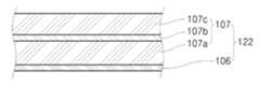
제2막(122)은 제1막(111)으로부터 이격되어 배치되며, 제2 투명 도전층(106)과 편광판(107)로 이루어질 수 있다.The
제2 투명 도전층(106)은 제1 투명 전극층(105)에 대향하여 배치되며, 복수 개의 스페이서(108)에 의해 제1 투명 전극층(105)과의 간격이 유지된다. 제2 투명 도전층(106)은 제1 투명 도전층(105)과 같이 투명한 도전성 금속으로 이루어지며, ITO로 형성될 수 있다.The second transparent
도 2는 제2막(122)를 나타내는 개략적인 단면도이다. 도 2를 참조하면, 편광판(107)은 제2 투명 도전층(106) 상에 순차적으로 적층되어 배치되는 지연필름(retardation film)(107a), 접착층(107b), 및 선형 편광층(linear polarizer)(107c)으로 이루어질 수 있다. 외부에서 입사하는 광은 선형 편광 층(107c)에 의해 한 축 방향의 광만이 투과되며, 한 축 방향의 광은 지연필름(107a)에 의해 위상이 지연되어 유기 발광 디스플레이 패널(110)에 반사된다. 이와 같이 반사된 광은 위상이 지연되었으므로 선형 편광층(107c)을 투과하지 못한다. 따라서, 제2막(122)은 편광판 기능을 하며, 외부광 반사를 감소시킬 수 있다.2 is a schematic cross-sectional view illustrating the
터치 패널은, 특히 저항식 터치 패널은 서로 대향하는 상하 저항막에 전압이 인가된 상태에서 사용자가 상기 저항막을 눌러 2개의 저항막이 접촉하여 발생하는 접촉점에서의 전압 또는 전류의 변화를 읽어들이고 그 좌표값을 환산하여 작동된다. 일반적으로 저항막은 투명 절연층과 도전층이 적층된 구조를 갖는다. 도 1에 도시된 본 발명의 일 실시예에 따른 유기 발광 디스플레이 장치(100)에서, 봉지기판(103)과 제1 투명 도전층(105)은 하부 저항막 기능을 하며, 제2 투명 도전층(106)과 편광판(107)으로 이루어진 제2막(122)은 상부 저항막 기능을 한다. 이와 같이, 도 1의 실시예에서는 하부 저항막이 봉지기판(103)과 제1 투명 도전층(105)으로 이루어지므로 터치 패널(120)의 두께가 슬림화된다. 즉, 도 1의 실시예는 별도의 투명 절연층을 사용하지 않고 봉기기판(103) 상에 제1 투명 도전층(105)을 적층하여 하부 저항막 기능을 하므로 터치 패널(120)의 두께가 감소시키고 유기 발광 디스플레이 장치(100) 전체의 두께가 감소시킨다.In particular, the touch panel reads a change in voltage or current at a contact point generated by a user pressing the resistive film and touching the resistive film while a resistive touch panel has a voltage applied to opposing upper and lower resistive films. It works by converting the value. In general, the resistive film has a structure in which a transparent insulating layer and a conductive layer are laminated. In the organic light emitting
또한, 도 1에 도시된 실시예는 제2막(122)이 상부 저항막 기능을 하는데, 제2막(122)은 편광판(107)을 구비하므로, 터치 패널(120)이 편광 기능을 하게 되므로 별도의 편광필름을 구비할 필요가 없어지게 되어 유기 발광 디스플레이 장치(100)의 두께를 감소시킬 수 있다.In addition, in the embodiment illustrated in FIG. 1, since the
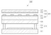
도 3은 본 발명의 다른 실시예에 따른 유기 발광 디스플레이 장치(200)를 개략적으로 나타내는 단면도이며, 도 4는 도 3에 도시된 제2막(222)의 단면도를 개략적으로 나타낸다.FIG. 3 is a schematic cross-sectional view of an organic light emitting
도 3을 참조하면, 본 발명의 다른 실시예에 따른 유기 발광 디스플레이 장치(200)는 유기 발광 디스플레이 패널(210) 및 터치 패널(220)을 구비한다.Referring to FIG. 3, an organic light emitting
유기 발광 디스플레이 패널(210)은 기판(101), 기판(101) 상에 배치되는 유기 발광부(102), 유기 발광부(102)를 봉지하는 봉지기판(103), 기판(101)과 봉지기판(103)을 합착하는 접착부재(104)를 구비한다.The organic light emitting
터치 패널(220)은 제1막(221), 제2막(222), 및 스페이서(108)을 구비한다. 제1막(222)은 봉지기판(103) 상에 배치되며, 투명 절연층(209)과 제1 투명 도전층(205)을 구비한다. 제2막(222)은 제2 투명 도전층(206)과 편광판(107)을 구비한다. 제1 및 2 투명 도전층(205, 206)은 ITO와 같은 투명 금속으로 형성된다.The
도 4를 참조하면, 제2막(222)은 제2 투명 도전층(206) 상에 순차적으로 적층된 지연필름(107a), 접착층(107b), 및 선형 편광층(107c)으로 이루어진다.Referring to FIG. 4, the
제1막(221)은 터치 패널(220)의 하부 저항막 기능을 하며, 제2막(222)은 터치 패널(220)의 상부 저항막 기능을 한다. 도 3에 도시된 실시예는 하부 저항막 기능을 하는 제2막(221)이 투명 절연층(209)와 제1 투명 도전층(205)로 이루어진다는 점에서 봉지기판(103)과 제1 투명 도전층(105)이 하부 저항막 기능하는 도 1에 도시된 실시예와 차이가 있다. 터치 패널(220)의 제2막(222)이 편광 기능을 한다는 점에서 별도의 편광판을 구비할 필요가 없으므로 유기 발광 디스플레이 장치(200)의 두께를 슬림화할 수 있다.The
투명 절연층(209)은 폴리에틸렌테레프탈레이트필름, 폴리카보네이트필름, 사이클릭올레핀코폴리머필름 또는 트리아세틸세룰로오스필름으로 이루어질 수 있다.The transparent
도 5는 본 발명의 또 다른 실시예에 따른 유기 발광 디스플레이 장치(300)를 개략적으로 나타내는 단면도이다.5 is a schematic cross-sectional view of an organic light emitting
도 5를 참조하면, 본 발명의 또 다른 실시예에 따른 유기 발광 디스플레이 장치(300)는 유기 발광 디스플레이 패널(310) 및 터치 패널(320)을 구비한다.Referring to FIG. 5, an organic light emitting
유기 발광 디스플레이 패널(310)은 기판(101), 기판(101) 상에 배치되는 유기 발광부(102), 유기 발광부(102)를 봉지하는 봉지기판(103), 기판(101)과 봉지기판(103)을 합착하는 접착부재(104)를 구비한다.The organic light emitting
터치 패널(320)은 제1막(321), 제2막(322), 및 스페이스(108)를 구비한다. 제1막(321)과 제2막(322)은 스페이스(108)에 의해 간격이 유지된다.The
제1막(321)은 봉지기판(103) 상에 배치되며, 제1 편광층(309)와 제1 투명 도전층(305)을 구비한다. 제2막(322)은 제2 투명 도전층(306)과 제2 편광층(307)을 구비한다. 제1 및 2 투명 도전층(305, 306)은 ITO와 같은 투명 금속으로 형성된다.The
제1막(321)은 터치 패널(320)의 하부 저항막 기능을 하며, 제2막(322)은 터치 패널(320)의 상부 저항막 기능을 한다.The
제1 편광층(309)은 지연필름으로 이루어지며, 제2 편광층(307)은 선형 편광층으로 이루어진다. 이와 같이 도 5의 실시예는 터치 패널(320)이 편광을 기능을 하므로 별도의 편광필름이 요구되지 않으므로 터치 패널(320)의 두께뿐만 아니라 유기 발광 디스플레이 장치(300)의 두께를 감소시킬 수 있다.The
본 발명은 상술한 실시형태 및 첨부된 도면에 의해 한정되는 것이 아니고, 첨부된 청구범위에 의해 한정하고자 하며, 청구범위에 기재된 본 발명의 기술적 사상을 벗어나지 않는 범위 내에서 다양한 형태의 치환, 변형 및 변경이 가능하다는 것은 당 기술분야의 통상의 지식을 가진 자에게 자명할 것이다.The present invention is not limited by the above-described embodiment and the accompanying drawings, but is intended to be limited by the appended claims, and various forms of substitution, modification, and within the scope not departing from the technical spirit of the present invention described in the claims. It will be apparent to those skilled in the art that changes are possible.
도 1은 본 발명의 일 실시예에 따른 유기 발광 디스플레이 장치(100)를 개략적으로 나타내는 단면도이다.1 is a cross-sectional view schematically illustrating an organic light emitting
도 2는 도 1에 도시된 제2막(122)을 개략적으로 나타내는 단면도이다.FIG. 2 is a cross-sectional view schematically illustrating the
도 3은 본 발명의 다른 실시예에 따른 유기 발광 디스플레이 장치(200)를 개략적으로 나타내는 단면도이다.3 is a schematic cross-sectional view of an organic light emitting
도 4는 도 3에 도시된 제2막(222)을 개략적으로 나타내는 단면도이다.4 is a cross-sectional view schematically illustrating the
도 5는 본 발명의 다른 실시예에 따른 유기 발광 디스플레이 장치(300)를 개략적으로 나타내는 단면도이다.5 is a schematic cross-sectional view of an organic light emitting
<도면의 주요부분에 대한 부호의 설명><Description of the symbols for the main parts of the drawings>
101: 기판102: 유기 발광부101: substrate 102: organic light emitting portion
103: 봉지기판104: 접착부재103: sealing substrate 104: adhesive member
105:제1 투명 도전층106: 제2 투명 도전층105: first transparent conductive layer 106: second transparent conductive layer
107: 편광판107: polarizer
110, 210, 310: 유기 발광 디스플레이 패널110, 210, 310: organic light emitting display panel
120, 220, 320: 터치 패널120, 220, 320: touch panel
Claims (14)
Translated fromKoreanPriority Applications (2)
| Application Number | Priority Date | Filing Date | Title |
|---|---|---|---|
| KR1020080113345AKR101065313B1 (en) | 2008-11-14 | 2008-11-14 | Organic light emitting display device |
| US12/506,162US8243034B2 (en) | 2008-11-14 | 2009-07-20 | Organic light emitting display device |
Applications Claiming Priority (1)
| Application Number | Priority Date | Filing Date | Title |
|---|---|---|---|
| KR1020080113345AKR101065313B1 (en) | 2008-11-14 | 2008-11-14 | Organic light emitting display device |
Publications (2)
| Publication Number | Publication Date |
|---|---|
| KR20100054419A KR20100054419A (en) | 2010-05-25 |
| KR101065313B1true KR101065313B1 (en) | 2011-09-16 |
Family
ID=42171621
Family Applications (1)
| Application Number | Title | Priority Date | Filing Date |
|---|---|---|---|
| KR1020080113345AActiveKR101065313B1 (en) | 2008-11-14 | 2008-11-14 | Organic light emitting display device |
Country Status (2)
| Country | Link |
|---|---|
| US (1) | US8243034B2 (en) |
| KR (1) | KR101065313B1 (en) |
Cited By (1)
| Publication number | Priority date | Publication date | Assignee | Title |
|---|---|---|---|---|
| WO2015076505A1 (en)* | 2013-11-20 | 2015-05-28 | 동우화인켐 주식회사 | Composite polarizing plate-integrated touch sensing electrode and touch screen panel having same |
Families Citing this family (17)
| Publication number | Priority date | Publication date | Assignee | Title |
|---|---|---|---|---|
| KR20120082736A (en) | 2011-01-14 | 2012-07-24 | 삼성모바일디스플레이주식회사 | Organic electroluminescence display apparatus |
| KR101908501B1 (en)* | 2011-12-07 | 2018-10-17 | 엘지디스플레이 주식회사 | Integrated Touch Screen With Organic Emitting Display Device and Method for Manufacturing the Same |
| US8937604B2 (en) | 2012-02-28 | 2015-01-20 | Eastman Kodak Company | Touch-responsive capacitor with polarizing dielectric structure |
| US8773395B2 (en) | 2012-04-24 | 2014-07-08 | Eastman Kodak Company | Touch-responsive capacitor with polarizing dielectric method |
| KR102056929B1 (en)* | 2013-03-08 | 2019-12-18 | 삼성디스플레이 주식회사 | Display Device Integrated Touch Screen Panel |
| KR101452302B1 (en) | 2013-07-29 | 2014-10-22 | 주식회사 하이딥 | Touch sensor panel |
| KR101681305B1 (en) | 2014-08-01 | 2016-12-02 | 주식회사 하이딥 | Touch input device |
| US10007380B2 (en) | 2013-07-29 | 2018-06-26 | Hideep Inc. | Touch input device with edge support member |
| KR101712346B1 (en) | 2014-09-19 | 2017-03-22 | 주식회사 하이딥 | Touch input device |
| JP6527343B2 (en) | 2014-08-01 | 2019-06-05 | 株式会社 ハイディープHiDeep Inc. | Touch input device |
| JP5845371B1 (en) | 2014-09-19 | 2016-01-20 | 株式会社 ハイディープ | smartphone |
| CN105761623B (en) | 2014-12-29 | 2019-03-08 | 乐金显示有限公司 | display device |
| KR102313489B1 (en)* | 2015-01-21 | 2021-10-18 | 삼성디스플레이 주식회사 | Touch panel and display apparatus having the same |
| KR102339300B1 (en)* | 2015-04-06 | 2021-12-15 | 삼성디스플레이 주식회사 | Flexible touch screen panel and flexible touch screen display device |
| KR101583765B1 (en) | 2015-07-27 | 2016-01-08 | 주식회사 하이딥 | Smartphone |
| KR102534273B1 (en)* | 2016-03-25 | 2023-05-19 | 삼성디스플레이 주식회사 | Flexible display device |
| CN109616491A (en)* | 2018-10-23 | 2019-04-12 | 武汉华星光电半导体显示技术有限公司 | a display panel |
Citations (2)
| Publication number | Priority date | Publication date | Assignee | Title |
|---|---|---|---|---|
| KR20040017138A (en)* | 2002-08-20 | 2004-02-26 | 삼성전자주식회사 | Image display device combined touch panel and method for manufacturing thereof |
| KR20080073559A (en)* | 2007-02-06 | 2008-08-11 | 삼성전자주식회사 | Organic electroluminescent display |
Family Cites Families (4)
| Publication number | Priority date | Publication date | Assignee | Title |
|---|---|---|---|---|
| US7405774B2 (en) | 2002-08-20 | 2008-07-29 | Samsung Electronics Co., Ltd. | Light guide plate and liquid crystal display having the same |
| JP4802896B2 (en)* | 2005-09-09 | 2011-10-26 | セイコーエプソン株式会社 | Manufacturing method of electro-optical device |
| JP5508662B2 (en)* | 2007-01-12 | 2014-06-04 | 株式会社半導体エネルギー研究所 | Display device |
| JP4989309B2 (en)* | 2007-05-18 | 2012-08-01 | 株式会社半導体エネルギー研究所 | Liquid crystal display |
- 2008
- 2008-11-14KRKR1020080113345Apatent/KR101065313B1/enactiveActive
- 2009
- 2009-07-20USUS12/506,162patent/US8243034B2/enactiveActive
Patent Citations (2)
| Publication number | Priority date | Publication date | Assignee | Title |
|---|---|---|---|---|
| KR20040017138A (en)* | 2002-08-20 | 2004-02-26 | 삼성전자주식회사 | Image display device combined touch panel and method for manufacturing thereof |
| KR20080073559A (en)* | 2007-02-06 | 2008-08-11 | 삼성전자주식회사 | Organic electroluminescent display |
Cited By (1)
| Publication number | Priority date | Publication date | Assignee | Title |
|---|---|---|---|---|
| WO2015076505A1 (en)* | 2013-11-20 | 2015-05-28 | 동우화인켐 주식회사 | Composite polarizing plate-integrated touch sensing electrode and touch screen panel having same |
Also Published As
| Publication number | Publication date |
|---|---|
| US8243034B2 (en) | 2012-08-14 |
| KR20100054419A (en) | 2010-05-25 |
| US20100123672A1 (en) | 2010-05-20 |
Similar Documents
| Publication | Publication Date | Title |
|---|---|---|
| KR101065313B1 (en) | Organic light emitting display device | |
| KR100987381B1 (en) | Organic light emitting display device | |
| US11442202B2 (en) | Foldable display device | |
| KR101058106B1 (en) | Display device | |
| KR101084169B1 (en) | Organic light emitting display device | |
| KR101127589B1 (en) | Organic light emitting display apparatus and the manufacturing method thereof | |
| KR100964234B1 (en) | Organic light emitting display apparatus | |
| KR101050464B1 (en) | Display panel and manufacturing method thereof | |
| KR101050460B1 (en) | OLED display and manufacturing method thereof | |
| CN103389822B (en) | Flexible display apparatus and the method bent using this sensing | |
| US10061416B2 (en) | Touch control display device and a preparation method thereof | |
| US8928597B2 (en) | Organic light emitting display device | |
| CN102005162B (en) | Organic light emitting diode display and manufacturing method thereof | |
| TWI452690B (en) | Organic light emitting display device and manufacturing method thereof | |
| US10423260B2 (en) | Display device with input function | |
| KR102664582B1 (en) | Foldable display device | |
| US20120306812A1 (en) | Top-emitting oled display having transparent touch panel | |
| JP5601888B2 (en) | Touch screen display device | |
| US20140240614A1 (en) | Display device and method of manufacturing the same | |
| KR20150000361A (en) | Plastic window and organic light emitting display device comprising the same | |
| CN107037906A (en) | Touch display panel and touch display device | |
| KR20220064359A (en) | Organic light emitting display device | |
| KR20170079506A (en) | Organic light emitting diode display device | |
| CN111381704A (en) | Touch display module and electronic terminal |
Legal Events
| Date | Code | Title | Description |
|---|---|---|---|
| A201 | Request for examination | ||
| PA0109 | Patent application | Patent event code:PA01091R01D Comment text:Patent Application Patent event date:20081114 | |
| PA0201 | Request for examination | ||
| PG1501 | Laying open of application | ||
| E902 | Notification of reason for refusal | ||
| PE0902 | Notice of grounds for rejection | Comment text:Notification of reason for refusal Patent event date:20100623 Patent event code:PE09021S01D | |
| E902 | Notification of reason for refusal | ||
| PE0902 | Notice of grounds for rejection | Comment text:Notification of reason for refusal Patent event date:20101230 Patent event code:PE09021S01D | |
| E701 | Decision to grant or registration of patent right | ||
| PE0701 | Decision of registration | Patent event code:PE07011S01D Comment text:Decision to Grant Registration Patent event date:20110831 | |
| GRNT | Written decision to grant | ||
| PR0701 | Registration of establishment | Comment text:Registration of Establishment Patent event date:20110908 Patent event code:PR07011E01D | |
| PR1002 | Payment of registration fee | Payment date:20110909 End annual number:3 Start annual number:1 | |
| PG1601 | Publication of registration | ||
| FPAY | Annual fee payment | Payment date:20140901 Year of fee payment:4 | |
| PR1001 | Payment of annual fee | Payment date:20140901 Start annual number:4 End annual number:4 | |
| FPAY | Annual fee payment | Payment date:20180829 Year of fee payment:8 | |
| PR1001 | Payment of annual fee | Payment date:20180829 Start annual number:8 End annual number:8 | |
| FPAY | Annual fee payment | Payment date:20190822 Year of fee payment:9 | |
| PR1001 | Payment of annual fee | Payment date:20190822 Start annual number:9 End annual number:9 | |
| PR1001 | Payment of annual fee | Payment date:20200901 Start annual number:10 End annual number:10 | |
| PR1001 | Payment of annual fee | Payment date:20210825 Start annual number:11 End annual number:11 | |
| PR1001 | Payment of annual fee | Payment date:20240822 Start annual number:14 End annual number:14 |