KR101064090B1 - The light- - Google Patents
The light-Download PDFInfo
- Publication number
- KR101064090B1 KR101064090B1KR1020090111034AKR20090111034AKR101064090B1KR 101064090 B1KR101064090 B1KR 101064090B1KR 1020090111034 AKR1020090111034 AKR 1020090111034AKR 20090111034 AKR20090111034 AKR 20090111034AKR 101064090 B1KR101064090 B1KR 101064090B1
- Authority
- KR
- South Korea
- Prior art keywords
- light emitting
- emitting device
- cavity
- device package
- light
- Prior art date
- Legal status (The legal status is an assumption and is not a legal conclusion. Google has not performed a legal analysis and makes no representation as to the accuracy of the status listed.)
- Expired - Fee Related
Links
Images


Classifications
- H—ELECTRICITY
- H10—SEMICONDUCTOR DEVICES; ELECTRIC SOLID-STATE DEVICES NOT OTHERWISE PROVIDED FOR
- H10H—INORGANIC LIGHT-EMITTING SEMICONDUCTOR DEVICES HAVING POTENTIAL BARRIERS
- H10H20/00—Individual inorganic light-emitting semiconductor devices having potential barriers, e.g. light-emitting diodes [LED]
- H10H20/80—Constructional details
- H10H20/85—Packages
- H10H20/855—Optical field-shaping means, e.g. lenses
- H10H20/856—Reflecting means
- H—ELECTRICITY
- H10—SEMICONDUCTOR DEVICES; ELECTRIC SOLID-STATE DEVICES NOT OTHERWISE PROVIDED FOR
- H10H—INORGANIC LIGHT-EMITTING SEMICONDUCTOR DEVICES HAVING POTENTIAL BARRIERS
- H10H20/00—Individual inorganic light-emitting semiconductor devices having potential barriers, e.g. light-emitting diodes [LED]
- H10H20/80—Constructional details
- H10H20/85—Packages
- H10H20/8506—Containers
- H—ELECTRICITY
- H01—ELECTRIC ELEMENTS
- H01L—SEMICONDUCTOR DEVICES NOT COVERED BY CLASS H10
- H01L2224/00—Indexing scheme for arrangements for connecting or disconnecting semiconductor or solid-state bodies and methods related thereto as covered by H01L24/00
- H01L2224/01—Means for bonding being attached to, or being formed on, the surface to be connected, e.g. chip-to-package, die-attach, "first-level" interconnects; Manufacturing methods related thereto
- H01L2224/42—Wire connectors; Manufacturing methods related thereto
- H01L2224/47—Structure, shape, material or disposition of the wire connectors after the connecting process
- H01L2224/48—Structure, shape, material or disposition of the wire connectors after the connecting process of an individual wire connector
- H01L2224/4805—Shape
- H01L2224/4809—Loop shape
- H01L2224/48091—Arched
- H—ELECTRICITY
- H01—ELECTRIC ELEMENTS
- H01L—SEMICONDUCTOR DEVICES NOT COVERED BY CLASS H10
- H01L2924/00—Indexing scheme for arrangements or methods for connecting or disconnecting semiconductor or solid-state bodies as covered by H01L24/00
- H01L2924/15—Details of package parts other than the semiconductor or other solid state devices to be connected
- H01L2924/181—Encapsulation
- H01L2924/1815—Shape
- H—ELECTRICITY
- H10—SEMICONDUCTOR DEVICES; ELECTRIC SOLID-STATE DEVICES NOT OTHERWISE PROVIDED FOR
- H10H—INORGANIC LIGHT-EMITTING SEMICONDUCTOR DEVICES HAVING POTENTIAL BARRIERS
- H10H20/00—Individual inorganic light-emitting semiconductor devices having potential barriers, e.g. light-emitting diodes [LED]
- H10H20/01—Manufacture or treatment
- H10H20/036—Manufacture or treatment of packages
- H—ELECTRICITY
- H10—SEMICONDUCTOR DEVICES; ELECTRIC SOLID-STATE DEVICES NOT OTHERWISE PROVIDED FOR
- H10H—INORGANIC LIGHT-EMITTING SEMICONDUCTOR DEVICES HAVING POTENTIAL BARRIERS
- H10H20/00—Individual inorganic light-emitting semiconductor devices having potential barriers, e.g. light-emitting diodes [LED]
- H10H20/80—Constructional details
- H10H20/85—Packages
- H10H20/855—Optical field-shaping means, e.g. lenses
Landscapes
- Led Device Packages (AREA)
Abstract
Translated fromKoreanDescription
Translated fromKorean실시 예는 발광소자 패키지에 관한 것이다.An embodiment relates to a light emitting device package.
Ⅲ-Ⅴ족 질화물 반도체(group Ⅲ-Ⅴ nitride semiconductor)는 물리적, 화학적 특성으로 인해 발광 다이오드(LED) 또는 레이저 다이오드(LD) 등의 발광 소자의 핵심 소재로 각광을 받고 있다. Ⅲ-Ⅴ족 질화물 반도체는 통상 InxAlyGa1-x-yN (0≤x≤1, 0≤y≤1, 0≤x+y≤1)의 조성식을 갖는 반도체 물질로 이루어져 있다.Group III-V nitride semiconductors are spotlighted as core materials of light emitting devices such as light emitting diodes (LEDs) or laser diodes (LDs) due to their physical and chemical properties. Ⅲ-Ⅴ nitride semiconductor is made of a semiconductor material having a compositional formula of normalIn x Al y Ga 1 -x- y N (0≤x≤1, 0≤y≤1, 0≤x + y≤1).
발광 다이오드(Light Emitting Diode : LED)는 화합물 반도체의 특성을 이용하여 전기를 적외선 또는 빛으로 변환시켜서 신호를 주고 받거나, 광원으로 사용되는 반도체 소자의 일종이다.A light emitting diode (LED) is a kind of semiconductor device that transmits and receives a signal by converting electricity into infrared light or light using characteristics of a compound semiconductor.
이러한 질화물 반도체 재료를 이용한 LED 혹은 LD는 광을 얻기 위한 발광 소자에 많이 사용되고 있으며, 핸드폰의 키패드 발광부, 전광판, 조명 장치 등 각종 제품의 광원으로 응용되고 있다.LEDs or LDs using such nitride semiconductor materials are widely used in light emitting devices for obtaining light, and have been applied to light sources of various products such as keypad light emitting units, electronic displays, and lighting devices of mobile phones.
실시 예는 새로운 구조를 갖는 발광소자 패키지를 제공한다.The embodiment provides a light emitting device package having a new structure.
실시 예는 넓은 지향각을 갖는 발광소자 패키지를 제공한다.The embodiment provides a light emitting device package having a wide directing angle.
실시 예는 투광성의 패키지 몸체를 갖는 발광소자 패키지를 제공한다.The embodiment provides a light emitting device package having a light transmissive package body.
실시 예에 따른 발광소자 패키지는, 상부 내측에 캐비티를 갖는 투광성의 패키지 몸체; 상기 캐비티에 배치된 복수의 리드 전극; 상기 캐비티 내에서 상기 리드 전극에 전기적으로 연결된 발광소자; 및 상기 발광소자 위에 수지물을 포함한다.According to an embodiment, there is provided a light emitting device package including: a transparent package body having a cavity inside an upper portion thereof; A plurality of lead electrodes disposed in the cavity; A light emitting device electrically connected to the lead electrode in the cavity; And a resin on the light emitting device.
실시 예는 새로운 구조를 갖는 발광소자 패키지를 제공할 수 있다.The embodiment can provide a light emitting device package having a new structure.
실시 예는 넓은 배광 분포를 갖는 발광소자 패키지를 제공할 수 있다.The embodiment can provide a light emitting device package having a wide light distribution.
실시 예는 색 편차를 개선시켜 줄 수 있는 발광소자 패키지를 제공할 수 있다.The embodiment can provide a light emitting device package that can improve color deviation.
실시예의 설명에 있어서, 각 층(막), 영역, 패턴 또는 구조물들이 기판, 각 층(막), 영역, 패드 또는 패턴들의 "상/위(on)"에 또는 "하/아래(under)"에 형성되는 것으로 기재되는 경우에 있어, "상/위(on)"와 "하/아래(under)"는 "직접(directly)" 또는 "다른 층을 개재하여 (indirectly)" 형성되는 것을 모두 포함 한다. 또한 각 층의 상/위 또는 하/아래에 대한 기준은 도면을 기준으로 설명한다.In the description of an embodiment, each layer, region, pattern or structure may be "under" or "under" the substrate, each layer, region, pad or pattern. In the case where it is described as being formed at, "up" and "under" include both "directly" or "indirectly" formed through another layer. do. In addition, the criteria for up / down or down / down each layer will be described with reference to the drawings.
도면에서 각층의 두께나 크기는 설명의 편의 및 명확성을 위하여 과장되거나 생략되거나 또는 개략적으로 도시되었다. 또한 각 구성요소의 크기는 실제크기를 전적으로 반영하는 것은 아니다.In the drawings, the thickness or size of each layer is exaggerated, omitted, or schematically illustrated for convenience and clarity of description. In addition, the size of each component does not necessarily reflect the actual size.
이하, 첨부된 도면을 참조하여 실시예에 따른 발광 소자 패키지에 대해 상세히 설명하도록 한다.Hereinafter, a light emitting device package according to an embodiment will be described in detail with reference to the accompanying drawings.
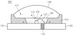
도 1은 제1실시예에 따른 발광 소자 패키지를 나타낸 측 단면도이다.1 is a side cross-sectional view illustrating a light emitting device package according to a first embodiment.
도 1을 참조하면, 발광 소자 패키지(100)는 제1캐비티(115), 제2캐비티(117), 제1 리드 전극(121), 제2 리드 전극(123), 패키지 몸체(110), 분리부(112), 발광 소자(125), 수지물(130), 및 렌즈부(140)를 포함한다.Referring to FIG. 1, the light
상기 패키지 몸체(110)는 투광성의 재료로서, 실리콘 또는 에폭시와 같은 수지 계열이거나, 유리 재질로 형성될 수 있다. 상기 패키지 몸체(110)의 외 형상은 원 기둥 형상, 다면체 형상 등으로 형성될 수 있으며, 이러한 형상은 몸체 재료의 사출 성형 또는/및 에칭 과정에 의해 변경될 수 있다. 실시 예에서 상기 패키지 몸체(110)는 대략 직육면체 형태로 형성되어, 적어도 한 구조의 캐비티가 형성된 것이 예시되어 있다.The
상기 제1 리드 전극(121)과 제2 리드 전극(123)은 서로 전기적으로 분리되고, 상기 패키지 몸체(110)를 관통하여 일측이 상기 제1 캐비티(115) 내로 노출되고 타측이 상기 패키지 몸체(110)의 외측으로 노출된다. 실시 예에서 상기 제1 리드 전극(121) 및 제2 리드 전극(123)은 각각 상기 패키지 몸체(110)의 외 측면에 하나 또는 복수로 분기되어 노출될 수 있다. 상기 제1 리드 전극(121) 및 제2 리드 전극(123)의 세 부분으로 분기되어 노출된 부분은 상기 패키지 몸체(110) 내에서 서로 전기적으로 연결된다.The
상기 제1리드 전극(121)과 상기 제2리드 전극(123)은 리드 프레임, 금속 도금층, 비아 구조 등을 선택적으로 이용하여 형성할 수 있으며, 설명의 편의를 위해 리드 프레임 타입을 그 예로 설명하기로 한다. 상기 제1리드 전극(121) 및 상기 제2리드 전극(123)은 일단이 상기 패키지 몸체(110)에 관통되게 배치되고 타단이 트리밍(trimming) 또는/및 포밍(froming)될 수 있으며, 이러한 트리밍 및 포밍 과정은 변경될 수 있다.The
상기 제1리드 전극(121) 및 상기 제2리드 전극(123)은 적어도 일부가 상기 패키지 몸체(110)의 하면에 노출되거나, 상기 하면과 동일 평면으로 연장될 수 있다.At least a portion of the
상기 패키지 몸체(110)의 제1캐비티(115)에는 상기 제1리드 전극(121) 및 상기 제2리드전극(123)의 일단이 배치될 수 있으며, 그 둘레는 제1캐비티(115)의 바닥면에 대해 수직하거나 경사지게 형성될 수 있다. 상기 제1캐비티(115)에는 발광 소자(125)가 배치되며, 상기 발광소자(125)는 적어도 한 리드 전극(121) 위에 배치될 수 있으며, 상기 제1리드 전극(121) 및 제2리드 전극(123)과 전기적으로 연결된다.One end of the
상기 제1리드 전극(121) 및 상기 제2리드 전극(123)은 분리부(112)에 의해 분리될 수 있다. 상기 분리부(112)는 상기 패키지 몸체(110)와 동일 재질일 수 있 으나, 광의 투과율인 낮은 재질 예컨대, 폴리머(Polymer)계 수지, 예를 들어, PPA(Polyphthal amide), LCP(Liquid Crystal Polymer), PPS(Poly Phenylene sulfide), 또는 PEEK(Polyetheretherketone) 등과 같은 재질이 이용될 수 있다.The
상기 분리부(112)는 상기 패키지 몸체(110)의 사출 성형하고 경화된 다음 형성될 수 있으며, 이러한 제조 과정에 대해 한정하지는 않는다.The
상기 분리부(112)는 상기 제1리드 전극(121)과 상기 제2리드 전극(123) 사이를 절연시켜 줄뿐만 아니라, 다른 영역 예컨대, 상기 제1리드 전극(121)의 내부 또는/및 상기 제2리드 전극(123)의 내부에 소정 크기로 형성될 수 있다. 이에 따라 상기 패키지 몸체(110)의 아래에 상기 제1리드 전극(121)과 상기 제2리드 전극(123)이 지지될 수 있다.The
상기 제1리드전극(121)과 상기 제2리드전극(123)의 영역 크기는 상기 패키지 몸체(110)의 하부 영역의 80% 이상으로 형성될 수 있으며, 그 상면은 각 반사를 수행하게 된다. 또한 상기 제1리드 전극(121), 상기 제2리드 전극(123) 및 상기 분리부(112)의 영역 크기는 상기 패키지 몸체(110)를 커버할 수 있으며, 상기 패키지 몸체(110)의 하부로 광이 누설되는 것을 방지할 수 있다.An area size of the
상기 제1 리드 전극(121) 및 제2 리드 전극(123)은 상기 발광 소자(125)에 전원을 제공하는 역할 외에도 상기 발광 소자(125)에서 발생된 열을 방출하는 역할과 상기 발광 소자(125)에서 발생된 빛을 반사시키는 역할을 할 수 있다.In addition to providing power to the
상기 제1캐비티(115)에는 적어도 하나의 발광 소자(125)가 배치될 수 있으며, 복수의 LED 칩이 탑재되면 상기 리드 전극(121,123)의 패턴은 변경될 수 있다.At least one
상기 발광 소자(125)는 칩 종류에 따라 하나 또는 그 이상의 와이어(127)를 이용한 와이어 본딩 방식, 또는 플립 또는 다이 본딩 방식을 선택적으로 이용하여 상기 제1리드 전극(121) 및 제2리드 전극(123)에 연결될 수 있다.The
상기 발광 소자(125)는 LED 칩으로서, 청색 LED(light emitting diode) 칩, 녹색 LED 칩, 적색 LED 칩과 같은 유색의 LED 칩을 포함하거나, UV(Ultraviolet) LED 칩을 포함할 수 있다. 실시 예는 청색 LED 칩을 그 예로 설명하기로 한다.The
상기 패키지 몸체(110)에는 제2캐비티(117)가 형성될 수 있으며, 상기 제2캐비티(117)는 상기 패키지 몸체(110)의 상부에 배치되며, 상기 제1캐비티(115)는 상기 제2캐비티(117)의 중앙 하부에 배치된다. 상기 제2캐비티(117)는 상기 제1캐비티(115) 위에 형성될 수 있다. 상기 제2캐비티(117)의 직경은 상기 제1캐비티(115)의 상부 직경보다 크게 형성될 수 있다.A
상기 제1캐비티(115) 또는/및 제2캐비티(117)의 공간은 상기 패키지 몸체(110) 또는/및 적어도 하나의 리드 전극(121,123)에 의해 형성될 수 있으며, 이러한 캐비티 공간은 실시 예의 기술적 범위 내에서 다양하게 변경될 수 있다.The space of the
상기 제1캐비티(115)에는 수지물(130)이 형성된다. 상기 수지물(130)은 실리콘 또는 에폭시 재료와 같은 투광성 수지 재료를 포함할 수 있으며, 상기 수지물(130)에는 적어도 한 종류의 형광체 또는/및 확산제가 첨가될 수 있으며, 이에 대해 한정하지는 않는다. 상기 형광체는 황색 형광체, 녹색 형광체, 적색 형광체, 및 청색 형광체를 포함할 수 있다. 상기 제1캐비티(115) 내의 LED 칩과 형광체의 종류는 패키지의 타켓 광에 따라 변경될 수 있으며, 이에 대해 한정하지는 않는다.The
상기 수지물(130)의 표면은 오목한 형상, 볼록한 형상, 또는 플랫한 형상으로 형성될 수 있으며, 그 표면에 패턴이 형성될 수 있다.The surface of the
상기 패키지 몸체(110) 내의 제1 캐비티(115) 및 상기 제2 캐비티(117)는 평면상의 형태가 원 형태 또는 다각형 형태를 갖는 홈 형태로 형성될 수 있으며, 상기 발광 소자(125)에서 방출된 광의 일부는 상기 제1캐비티(115)의 둘레 면에서 반사되거나 투과될 수 있다. 상기 렌즈부(140)로 진행하는 광의 대부분은 상 방향으로 방출되고, 상기 패키지 몸체(110)로 진행하는 광은 투과되어 사이드 방향으로 방출된다.The
또한 상기 제1리드전극(121) 및 상기 제2리드 전극(123)에 의해 반사된 광은 상기 패키지 몸체(110)를 통해 렌즈부(140)로 진행할 수 있다.In addition, the light reflected by the first
이에 따라 상기 발광 소자 패키지(100)는 상기 제1리드 전극(121) 및 상기 제2리드 전극(123)의 연장 선상 위로 광이 방출되는 분포를 가지게 되어, 그 배광 분포는 160~180도의 지향각으로 조사된다.Accordingly, the light emitting
상기 수지물(130)과 상기 렌즈부(140) 사이에는 다른 투광성 수지층 또는 투광성 형광체층을 포함할 수 있으며, 이에 대해 한정하지는 않는다.Between the
상기 렌즈부(140)는 상기 수지물(130) 및 상기 패키지 몸체(110) 상에 배치되어 상기 발광 소자(125)에서 방출된 광을 외부로 출사시켜 주는 데, 이때 광의 지향각을 변화시키는 렌즈 역할을 한다. 상기 렌즈부(140)는 상기 제2캐비티(117)에 실리콘 또는 에폭시와 같은 수지 재질, 고분자 물질 또는 유리 재료를 포함하여 형성될 수 있다. 또한, 상기 렌즈부(140)는 적어도 일부분에 형광체 또는 색 변환 물질을 포함할 수도 있다.The
상기 렌즈부(140)는 상기 제2캐비티(117)에 형성되어, 그 상부가 볼록 렌즈 형상으로 형성될 수 있다. 상기 렌즈부(140)는 상기 제2캐비티(117)에 수지 재료로 형성되거나 별도의 렌즈를 부착하여 형성될 수 있다. 또한 상기 제1캐비티(115) 및 제2 캐비티(117) 중 어느 하나는 형성하지 않을 수 있고 상기 발광 소자(125)의 위치도 변경될 수 있다.The
상기 렌즈부(140)는 상기 발광 소자(125)와 직접 접촉되거나 이격되어 배치될 수 있으며, 그 일부가 상기 제1캐비티(115) 영역에 배치될 수 있으며, 이에 대해 한정하지는 않는다.The
상기 발광 소자 패키지(100)는 투광성의 패키지 몸체(110)에 의해 지향각을 넓힐 수 있고, 배광 영역에서의 각 지향각 별 색편차를 개선시켜 줄 수 있다.The light emitting
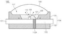
도 2는 제2실시 예에 따른 발광소자 패키지를 나타낸 측 단면도이다. 제2실시 예를 설명함에 있어서, 제1실시 예에 동일한 부분에 대해서는 제1실시 예를 참조하며 중복 설명은 생략하기로 한다.2 is a side cross-sectional view illustrating a light emitting device package according to a second embodiment. In the description of the second embodiment, the same parts as in the first embodiment are referred to the first embodiment, and redundant description thereof will be omitted.
도 2를 참조하면, 발광 소자 패키지(100A)는 투광성 패키지 몸체(110) 위에 렌즈부(140A)의 형상을 측면 반사형 렌즈로 제공한 구조이다. 상기 렌즈부(140A)는 소정 부위 예컨대, 중앙부에 함몰부(145)를 구비하여 소정 깊이의 홈으로 형성된다. 상기 렌즈부(140A)는 상기 패키지 몸체(110)의 상부에 노출된 부분이 반구 형태로 형성될 수 있고, 상기 함몰부(145)는 상기 렌즈부(140A)의 중앙부에서 상기 발광 소자(50)와 수직 방향으로 오버랩되는 되는 부분에 형성될 수 있어, 입사되는 광을 모든 측 방향으로 반사시켜 줄 수 있다.Referring to FIG. 2, the light emitting
상기 렌즈부(140A)의 함몰부(145)는 렌즈 중앙에 형성되거나 발광 소자(125) 위에 대응되는 위치에 형성될 수 있다. 상기 함몰부(145)의 표면 형상이 원형 또는 다각형 형상으로 형성될 수 있으며, 그 직경은 상기 발광 소자(125)가 배치되는 하 방향으로 내려갈수록 점차 좁아지게 형성된다.The
또한 상기 패키지 몸체(110)의 제1캐비티(115A)는 그 둘레가 수직한 면으로 형성되며, 상기 수직한 면은 상기 발광 소자(125)로부터 방출된 광이 상기 패키지 몸체(110)로 입사되도록 할 수 있으며, 그 투과량은 경사진 면에 비해 증가될 수 있다.In addition, the
상기 발광 소자 패키지(100A)는 측 방향으로 진행하는 광을 증가시켜 줌으로써, 넓은 지향각과 함게 배광 영역에서의 색 편차를 줄여줄 수 있다.The light emitting
도 3은 도 2의 변형 예이다.3 is a modification of FIG. 2.
도 3을 참조하면, 발광 소자 패키지(100A)는 렌즈부(140A)를 변경한 구조이다. 상기 렌즈부(140A)의 외측 하부(S2)는 상기 패키지 몸체(110)의 외측까지 연장되어 형성되며, 상기 패키지 몸체(110)의 상부 및 외측 하부(S2)로 방출된 광을 굴절시켜 줄 수 있다. 상기 렌즈부(140A)는 수지 재질로 형성되며, 그 외측 하부(S2)가 복수의 리드 전극(121,123)의 외측 상면에 접촉되기 때문에, 상기 패키지 몸체(110)의 외측으로의 습기 침투를 억제할 수 있다. 상기 발광 소자 패키지(100A)는 투광성의 패키지 몸체(110)와 상기 렌즈부(140A)에 의해 지향각이 개선될 수 있 다.Referring to FIG. 3, the light emitting
도 4는 제3실시 예에 따른 발광소자 패키지를 나타낸 측 단면도이다. 제3실시 예를 설명함에 있어서, 제1실시 예에 동일한 부분에 대해서는 제1실시 예를 참조하며 중복 설명은 생략하기로 한다. 4 is a side cross-sectional view illustrating a light emitting device package according to a third embodiment. In the description of the third embodiment, the same parts as in the first embodiment are referred to the first embodiment, and redundant description thereof will be omitted.
도 4를 참조하면, 발광 소자 패키지(100B)는 소정 형상의 패턴(142)을 갖는 렌즈부(140B)를 포함한다. 상기 렌즈부(140B)의 상면에는 복수의 패턴(142)이 형성되며, 상기 복수의 패턴(142)은 동심원 형상으로 배열된다. 상기 동심원 형상의 패턴(142)은 상기 렌즈부(140B)의 상면 전체에 형성되거나, 상면 중심부, 상면 둘레부, 또는 상면 중심부와 상면 둘레부 사이의 영역 중 적어도 한 영역에 형성될 수 있다. 이하, 실시 예는 상기 동심원 형상의 패턴(142)이 상기 렌즈부(140B)의 전체 상면에 배치되는 것을 그 예로 설명하기로 하며, 이로 한정하는 것은 아니다.Referring to FIG. 4, the light emitting
상기 렌즈부(140B)의 동심원 형상의 패턴(142)은 상면 중앙을 중심으로 하고 서로 다른 직경을 갖는 원 형상, 타원 형상, 비구면 형상, 및 다각 형상 중 적어도 한 형상을 갖고 돌출되는 형태이다. 상기 동심원 형상의 패턴(142)은 상기 렌즈부(140B)의 표면 형상에 따라 서로 다른 평면상에 배치되거나, 동일 평면상에 배치될 수 있다. 상기 각 패턴(142)의 형상은 대칭 또는 비대칭의 다각 뿔 형상 또는 프리즘 패턴으로 형성될 수 있다.The
상기 동심원 형상의 패턴(142)은 상기 렌즈부(140B)의 상면 형상을 따라 형성되며, 각 패턴의 크기는 상기 렌즈부(140B)의 상면 중앙부터 외측 방향으로 갈수록 점차 작아지도록 형성되거나, 각 패턴의 높이는 상기 렌즈 중앙으로부터 외측 방향으로 갈수록 점차 낮아지도록 형성될 수 있다.The
상기 동심원 형상의 패턴(142)은 프리즘 패턴의 형상을 포함하며, 각 패턴 간의 간격은 일정한 간격, 불규칙한 간격, 또는 랜덤한 간격으로 배열될 수 있다.The
상기 렌즈부(140B)의 동심원 형상의 패턴(142)은 상기 발광 소자(125)로부터 방출된 광이 투과 또는 반사될 때 굴절 또는 분산시켜 줌으로써, 상기 렌즈부(140)의 중앙부와 사이드부의 광이 균일한 광도의 분포를 가질 수 있다. 또한 상기 렌즈부(140B)의 중앙부와 사이드부 사이의 색편차가 거의 존재하지 않으며, 이러한 색 편차의 정도는 상기 동심원 형상의 패턴(142)에 의해 달라질 수 있다.The
도 5는 도 4의 변형 예이다.5 is a modified example of FIG. 4.
도 5를 참조하면, 발광 소자 패키지(100B)는 패키지 몸체(110A)의 형상을 일단의 캐비티(115)를 갖는 형상으로 변경하고, 상기 렌즈부(140B)의 외측 하부(S4)를 패키지 몸체(110A)의 둘레로 더 연장하여 배치하게 된다. 상기 렌즈부(140B)의 외측 하부(S4)는 상기 패키지 몸체(110A)의 외측 둘레 및 상기 리드 전극(121,123)의 상면까지 연장되므로, 동심원 형상의 패턴(142)이 패키지 몸체(110A)의 둘레까지 커버할 수 있다.Referring to FIG. 5, the light emitting
상기 렌즈부(140B)는 상기 발광 소자(125)로부터 방출된 광이 전 방향으로 투과될 때 굴절 또는 반사시켜 줌으로써, 상기 렌즈부(140B)의 중앙부와 사이드부의 광이 균일한 광도의 분포를 가질 수 있다. 또한 상기 렌즈부(140B)의 중앙부와 사이드부 사이의 색편차가 거의 존재하지 않으며, 이러한 색 편차의 정도는 상기 동심원 형상의 패턴(142)에 의해 달라질 수 있다.The
도 6은 도 5의 변형 예이다.6 is a modified example of FIG. 5.
도 6을 참조하면, 발광 소자 패키지(100B)는 렌즈부(140B)의 상측에는 동심원 형상의 패턴(142)이 형성되고, 외측 하부(S6)는 상기 패턴이 형성되지 않는 비 패턴 영역으로 형성될 수 있다. 이에 따라 렌즈부(140B)는 상기 발광 소자(125)로부터 방출된 광을 굴절 또는 반사시켜 주며, 그 상측의 동심원 형상의 패턴(142)에 의해 균일한 분포의 색 편차를 가지게 되고, 외측 하부(S6)의 비 패턴 영역에 의해 광의 지향각 분포를 개선시켜 줄 수 있다.Referring to FIG. 6, in the light emitting
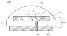
도 7은 제4실시 예에 따른 발광소자 패키지를 나타낸 측 단면도이다. 제4실시 예를 설명함에 있어서, 제1실시 예에 동일한 부분에 대해서는 제1실시 예를 참조하며 중복 설명은 생략하기로 한다.7 is a side cross-sectional view illustrating a light emitting device package according to a fourth embodiment. In the description of the fourth embodiment, the same parts as in the first embodiment will be described with reference to the first embodiment, and redundant description thereof will be omitted.
도 7을 참조하면, 발광 소자 패키지(100C)는 몸체 상부(101) 및 몸체 하부(102)를 포함하는 패키지 몸체(110B)를 포함한다.Referring to FIG. 7, the light emitting
상기 패키지 몸체(110B)의 몸체 상부(101)는 제1실시 예에 개시된 투광성 재료이고, 상기 몸체 하부(102)는 상기 투광성 재료이거나, 비 투광성 재료 예컨대, 폴리머 계열로 형성될 수 있다. 상기 몸체 하부(102)와 상기 몸체 상부(101)는 제1리드 전극(121)과 제2리드 전극(123)의 관통하여 서로 접촉될 수 있으며, 그 접촉된 영역은 적어도 한 영역이 될 수 있다.The
상기 패키지 몸체(110B)에는 분리부(112A)가 형성되며, 상기 분리부(112A)는 상기 제1리드 전극(121) 및 제2리드 전극(123) 사이에 형성되며, 상기 몸체 하부(102)를 통해 상기 몸체 하부(102)의 하면과 동일 평면으로 배치될 수 있다. 이 경우, 상기 패키지 몸체(110B)의 몸체 하부(102)를 형성한 다음, 상기 분리부(112A)를 형성할 수 있다.A
여기서, 상기 몸체 하부(102)가 폴리머 재질인 경우, 상기 분리부(112A)는 상기 몸체 하부(102)와 동일한 재질로 형성될 수 있다.Here, when the body
상기 제1리드전극(121) 및 상기 제2리드전극(123)은 몸체 상부(101) 및 몸체 하부(102) 사이에 지지되며, 상기 분리부(112A)와 함께 하부로 진행하는 광을 반사시켜 줄 수 있다.The first
이에 따라 상기 발광소자 패키지(100C)는 상기 투광성의 몸체 상부(101), 상기 수지물(130), 상기 렌즈부(140)로 진행하는 광이 전 영역으로 분산되고 투과됨으로써, 배광 영역에서의 색 좌표 편차를 개선시켜 줄 수 있다.Accordingly, in the light emitting
도 8은 도 7의 변형 예이다.8 is a modified example of FIG.
도 8을 참조하면, 발광 소자 패키지(100C)는 렌즈부(140)의 외측 하부(S8)를 상기 몸체 상부(101)의 외측 둘레까지 연장한 구조이다. 상기 렌즈부(140)의 외측 하부(S8)는 상기 몸체 상부(101)에 이격되며, 상기 제1리드 전극(121) 및 제2리드 전극(123)의 외측 상면과 접촉되며, 습기 침투 및 광 지향각을 개선시켜 줄 수 있다.Referring to FIG. 8, the light emitting
도 9는 제5실시 예에 따른 발광소자 패키지를 나타낸 사시도이다. 제5실시 예를 설명함에 있어서, 제1실시 예에 동일한 부분에 대해서는 제1실시 예를 참조하며 중복 설명은 생략하기로 한다.9 is a perspective view illustrating a light emitting device package according to a fifth embodiment. In the description of the fifth embodiment, the same parts as in the first embodiment will be referred to the first embodiment, and redundant description thereof will be omitted.
도 9를 참조하면, 발광 소자 패키지(200)는 패키지 몸체(210), 몸체 하부(201), 제1리드 전극(221), 제2리드 전극(223), 발광 소자(225), 수지물(230), 및 렌즈부(240)를 포함한다.9, the light emitting
상기 제1리드 전극(221)은 일단이 상기 제2캐비티(117)의 바닥면 일부에 배치되고, 타단이 패키지 몸체(210)의 타측 방향으로 연장되어 몸체 하부(201)의 하면에 위치한다.One end of the first
상기 제2리드 전극(223)은 타단이 상기 제2캐비티(117) 바닥면에서 상기 제1리드 전극(221)과 분리되며, 상기 패키지 몸체(210)의 내측 제1캐비티(215)를 형성하게 된다. 상기 제2리드 전극(223)의 일단은 상기 패키지 몸체(210)를 통해 연장되어 상기 몸체 하부(201)의 하면에 위치한다.The other end of the second
이에 따라 상기 제2리드 전극(223)는 상기 발광 소자(215)가 배치되고, 발광 소자(215)는 와이어 본딩 또는/및 다이 본딩 등에 의해 상기 제1리드전극(221) 및 제2리드전극(223)에 연결될 수 있다.Accordingly, the
상기 제1리드전극(221) 및 상기 제2리드전극(223)의 외측 상부에는 상기 패키지 몸체(210)가 배치되어, 그 내부에 상기 제1캐비티(215)와 연통되는 제2캐비티(217)를 형성하게 된다.The
상기 패키지 몸체(210)는 투광성 재료로서, 실리콘 또는 에폭시와 같은 수지 재료이거나 유리 재료로 구현될 수 있다.The
상기 패키지 몸체(210), 상기 제1 및 제2리드 전극(221,223)의 하부에는 몸체 하부(201)가 형성되는 데, 상기 몸체 하부(201)는 비 투광성 재질로서, 상기에 개시된 분리부의 재질로 이루어질 수 있다.A lower portion of the
상기 발광 소자(215)는 상기 제2리드 전극(223)으로 이루어지는 제1캐비티(215) 영역 내에 배치되고, 상기 제1캐비티(215)에는 실리콘 또는 에폭시와 같은 투광성 수지물(230)이 형성된다. 상기 수지물(230) 위에는 렌즈부(240)가 형성되며, 상기 렌즈부(240)는 중앙부에 함몰부(242)를 갖는 측면 반사형 렌즈 형상으로 형성될 수 있다.The
상기 발광 소자(215)로부터 방출된 광은 상면 및 측 방향으로 진행하며, 상기 측 방향으로 진행하는 광은 상기 제2리드 전극(223)에 의해 상 방향으로 진행하게 되며, 상기 상 방향으로 진행하는 광의 일부는 상기 렌즈부(240)의 함몰부(242)에 의해 주변 방향으로 반사되고 다른 광은 외부로 투과된다. The light emitted from the
상기 렌즈부(240)의 함몰부(242)에 의해 반사된 광은 패키지 몸체(210)를 투과하여 상기 제1 및 제2리드전극(221,223)에 의해 반사되어, 진행하게 된다.The light reflected by the
이러한 발광 소자 패키지(200)는 발광 소자(215)로부터 방출된 광 중에서 측 방향으로 진행하는 일부 광은 제2리드전극(223)에 의해 반사시켜 주고, 또 상 방향으로 일부 광은 상기 렌즈부(240)에 의해 하 방향으로 반사시켜 줌으로써, 넓은 지향각을 갖는 배광 분포로 발광하게 된다. 이러한 배광 분포에서는 렌즈 중앙과 사이드 사이의 색 편차가 개선될 수 있다.The light emitting
이상에서 실시예들에 설명된 특징, 구조, 효과 등은 본 발명의 적어도 하나의 실시예에 포함되며, 반드시 하나의 실시예에만 한정되는 것은 아니다. 나아가, 각 실시예에서 예시된 특징, 구조, 효과 등은 실시예들이 속하는 분야의 통상의 지식을 가지는 자에 의해 다른 실시예들에 대해서도 조합 또는 변형되어 실시 가능하다. 따라서 이러한 조합과 변형에 관계된 내용들은 본 발명의 범위에 포함되는 것으로 해석되어야 할 것이다.Features, structures, effects, and the like described in the above embodiments are included in at least one embodiment of the present invention, and are not necessarily limited to only one embodiment. Furthermore, the features, structures, effects, and the like illustrated in the embodiments may be combined or modified with respect to other embodiments by those skilled in the art to which the embodiments belong. Therefore, it should be understood that the present invention is not limited to these combinations and modifications.
이상에서 실시예를 중심으로 설명하였으나 이는 단지 예시일 뿐 본 발명을 한정하는 것이 아니며, 본 발명이 속하는 분야의 통상의 지식을 가진 자라면 본 실시예의 본질적인 특성을 벗어나지 않는 범위에서 이상에 예시되지 않은 여러 가지의 변형과 응용이 가능함을 알 수 있을 것이다. 예를 들어, 실시예에 구체적으로 나타난 각 구성 요소는 변형하여 실시할 수 있는 것이다. 그리고 이러한 변형과 응용에 관계된 차이점들은 첨부된 청구 범위에서 규정하는 본 발명의 범위에 포함되는 것으로 해석되어야 할 것이다.Although the above description has been made based on the embodiments, these are merely examples and are not intended to limit the present invention. Those skilled in the art to which the present invention pertains may not have been exemplified above without departing from the essential characteristics of the present embodiments. It will be appreciated that many variations and applications are possible. For example, each component specifically shown in the embodiment can be modified. And differences relating to such modifications and applications will have to be construed as being included in the scope of the invention defined in the appended claims.
도 1은 제1실시 예에 따른 발광소자 패키지의 측 단면도이다.1 is a side cross-sectional view of a light emitting device package according to a first embodiment.
도 2는 제2실시 예에 따른 발광소자 패키지의 측 단면도이다.2 is a side cross-sectional view of a light emitting device package according to a second embodiment.
도 3은 도 2의 변형 예이다.3 is a modification of FIG. 2.
도 4는 제3실시 예에 따른 발광소자 패키지의 측 단면도이다.4 is a side cross-sectional view of a light emitting device package according to a third embodiment.
도 5는 도 4의 변형 예이다.5 is a modified example of FIG. 4.
도 6은 도 5의 변형 예이다.6 is a modified example of FIG. 5.
도 7은 제4실시 예에 따른 발광소자 패키지의 측 단면도이다.7 is a side cross-sectional view of a light emitting device package according to a fourth embodiment.
도 8은 도 7의 변형 예이다.8 is a modified example of FIG.
도 9는 제5실시 예에 따른 발광소자 패키지의 부분 단면을 나타낸 사시도이다.9 is a perspective view showing a partial cross section of the light emitting device package according to the fifth embodiment.
Claims (14)
Translated fromKoreanPriority Applications (6)
| Application Number | Priority Date | Filing Date | Title |
|---|---|---|---|
| KR1020090111034AKR101064090B1 (en) | 2009-11-17 | 2009-11-17 | The light- |
| US12/947,282US8530918B2 (en) | 2009-11-17 | 2010-11-16 | Light emitting device package and lighting system |
| EP10191573.4AEP2323183B1 (en) | 2009-11-17 | 2010-11-17 | Light emitting device package |
| CN201010551198.4ACN102097423B (en) | 2009-11-17 | 2010-11-17 | Light emitting device package and illuminator |
| JP2010256647AJP5797393B2 (en) | 2009-11-17 | 2010-11-17 | Light emitting device package |
| US14/013,882US8835969B2 (en) | 2009-11-17 | 2013-08-29 | Light emitting device package and lighting system |
Applications Claiming Priority (1)
| Application Number | Priority Date | Filing Date | Title |
|---|---|---|---|
| KR1020090111034AKR101064090B1 (en) | 2009-11-17 | 2009-11-17 | The light- |
Publications (2)
| Publication Number | Publication Date |
|---|---|
| KR20110054411A KR20110054411A (en) | 2011-05-25 |
| KR101064090B1true KR101064090B1 (en) | 2011-09-08 |
Family
ID=43597827
Family Applications (1)
| Application Number | Title | Priority Date | Filing Date |
|---|---|---|---|
| KR1020090111034AExpired - Fee RelatedKR101064090B1 (en) | 2009-11-17 | 2009-11-17 | The light- |
Country Status (5)
| Country | Link |
|---|---|
| US (2) | US8530918B2 (en) |
| EP (1) | EP2323183B1 (en) |
| JP (1) | JP5797393B2 (en) |
| KR (1) | KR101064090B1 (en) |
| CN (1) | CN102097423B (en) |
Cited By (1)
| Publication number | Priority date | Publication date | Assignee | Title |
|---|---|---|---|---|
| KR101356475B1 (en)* | 2013-03-27 | 2014-01-29 | 한국생산기술연구원 | High performance led substrate and method of manufacturing the same |
Families Citing this family (50)
| Publication number | Priority date | Publication date | Assignee | Title |
|---|---|---|---|---|
| KR101693642B1 (en)* | 2010-12-21 | 2017-01-17 | 삼성전자 주식회사 | Manufacturing method of Light emitting device package |
| CN103299441B (en)* | 2011-01-20 | 2016-08-10 | 夏普株式会社 | The manufacture method of light-emitting device, illuminator, display device and light-emitting device |
| TWI517452B (en)* | 2011-03-02 | 2016-01-11 | 建準電機工業股份有限公司 | Polycrystalline package structure of luminescent crystal |
| CN102655198B (en)* | 2011-03-03 | 2015-09-23 | 展晶科技(深圳)有限公司 | LED source |
| US9029887B2 (en) | 2011-04-22 | 2015-05-12 | Micron Technology, Inc. | Solid state lighting devices having improved color uniformity and associated methods |
| KR101852388B1 (en)* | 2011-04-28 | 2018-04-26 | 엘지이노텍 주식회사 | Light emitting device package |
| US8878215B2 (en)* | 2011-06-22 | 2014-11-04 | Lg Innotek Co., Ltd. | Light emitting device module |
| KR101880454B1 (en)* | 2011-08-24 | 2018-07-23 | 엘지이노텍 주식회사 | Light emitting device package |
| US9397274B2 (en) | 2011-08-24 | 2016-07-19 | Lg Innotek Co., Ltd. | Light emitting device package |
| KR101896659B1 (en)* | 2011-09-02 | 2018-09-07 | 엘지이노텍 주식회사 | Light emitting device package, back light unit and display unit |
| KR101896661B1 (en)* | 2011-10-28 | 2018-09-07 | 엘지이노텍 주식회사 | Light emitting device package, back light unit and display unit |
| KR101896662B1 (en)* | 2011-11-07 | 2018-09-07 | 엘지이노텍 주식회사 | Light emitting device package, back light unit and display unit |
| KR101905535B1 (en) | 2011-11-16 | 2018-10-10 | 엘지이노텍 주식회사 | Light emitting device and light apparatus having thereof |
| CN104054189B (en)* | 2011-11-17 | 2018-06-26 | 株式会社流明斯 | Light-emitting element package and backlight unit including the light-emitting element package |
| KR101949150B1 (en)* | 2011-12-06 | 2019-02-18 | 엘지이노텍 주식회사 | Light emitting device package |
| KR101890733B1 (en)* | 2012-03-19 | 2018-08-22 | 엘지디스플레이 주식회사 | Light emitting diode package |
| WO2013180365A1 (en) | 2012-05-31 | 2013-12-05 | Lg Innotek Co., Ltd. | Member for cotrolling luminous flux, method for fabricating the member, display device, and light emitting device |
| CN102832321A (en)* | 2012-08-29 | 2012-12-19 | 苏州金科信汇光电科技有限公司 | Surface-mounted laser packaging structure |
| KR101360568B1 (en)* | 2012-09-14 | 2014-02-11 | 엘지이노텍 주식회사 | Optical member and display device having the same |
| KR101373352B1 (en)* | 2012-09-24 | 2014-03-13 | 창 와 테크놀러지 컴퍼니 리미티드 | Pre-process of encapsulating led and the encapsulated led |
| KR101413596B1 (en)* | 2012-12-07 | 2014-07-02 | 주식회사 루멘스 | Light emitting device and backlight unit comprising the same |
| KR101984897B1 (en)* | 2012-12-10 | 2019-06-03 | 삼성디스플레이 주식회사 | Light emitting diode package and manufacturing method thereof |
| US20140167074A1 (en)* | 2012-12-17 | 2014-06-19 | Waitrony Optoelectronics Limited | Intensity Scattering LED Apparatus |
| KR102029802B1 (en) | 2013-01-14 | 2019-10-08 | 엘지이노텍 주식회사 | Light emitting device and light apparatus having thereof |
| DE102013202551A1 (en) | 2013-02-18 | 2014-08-21 | Heraeus Materials Technologies GmbH & Co. KG | Substrate manufacturing method for LED chip in LED module, involves providing metal layer with cavity, and allowing edge of cavity of substrate to be deformable frontward through deformation that is thicker than metal layer |
| US9404647B2 (en) | 2013-03-15 | 2016-08-02 | Hubbell Incorporated | Class 1 compliant lens assembly |
| DE102013213073A1 (en)* | 2013-07-04 | 2015-01-08 | Osram Opto Semiconductors Gmbh | Method for producing an optoelectronic component |
| US9335023B2 (en)* | 2013-12-11 | 2016-05-10 | Shenzhen China Star Optoelectronics Technology Co., Ltd. | Quantum dot lens and manufacturing method thereof |
| DE102014101557A1 (en)* | 2014-02-07 | 2015-08-13 | Osram Opto Semiconductors Gmbh | Optoelectronic component and method for its production |
| KR102277125B1 (en) | 2014-06-09 | 2021-07-15 | 삼성전자주식회사 | Light source module, lighting device and lighting system |
| KR20160069724A (en)* | 2014-12-09 | 2016-06-17 | 엘지이노텍 주식회사 | Phosphor composition, light emitting device package and lighting apparatus including the same |
| KR102252994B1 (en)* | 2014-12-18 | 2021-05-20 | 삼성전자주식회사 | Light emitting device package and fluorescent film for the same |
| US10018324B2 (en)* | 2015-03-31 | 2018-07-10 | Koito Manufacturing Co., Ltd. | Light source unit with light emitting module, sealing part and lens part |
| KR102486035B1 (en)* | 2016-01-28 | 2023-01-06 | 쑤저우 레킨 세미컨덕터 컴퍼니 리미티드 | Light emitting device package and light emitting apparatus having the same |
| KR102558280B1 (en)* | 2016-02-05 | 2023-07-25 | 쑤저우 레킨 세미컨덕터 컴퍼니 리미티드 | Light source unit and light unit having thereof |
| JP6162280B1 (en)* | 2016-03-09 | 2017-07-12 | 株式会社エンプラス | Light emitting device and surface light source device |
| WO2018030757A1 (en) | 2016-08-09 | 2018-02-15 | 엘지이노텍 주식회사 | Light emitting module, flash module, and terminal including same |
| WO2018074866A2 (en)* | 2016-10-21 | 2018-04-26 | 주식회사 세미콘라이트 | Semiconductor light emitting device |
| KR102017734B1 (en)* | 2016-10-21 | 2019-09-03 | 주식회사 세미콘라이트 | Semiconductor light emitting device |
| CN106641750B (en)* | 2016-10-31 | 2023-10-13 | 易美芯光(北京)科技有限公司 | Light mixing system |
| EP3470730B1 (en) | 2017-10-10 | 2023-01-25 | ZG Lighting France S.A.S | Lighting unit and luminaire for road and/or street lighting |
| US20190267525A1 (en) | 2018-02-26 | 2019-08-29 | Semicon Light Co., Ltd. | Semiconductor Light Emitting Devices And Method Of Manufacturing The Same |
| KR102117627B1 (en)* | 2018-10-30 | 2020-06-01 | 주식회사 인터원 | RGB LED Module with optical lens |
| TWI703743B (en)* | 2018-10-31 | 2020-09-01 | 億光電子工業股份有限公司 | Lighting device and lighting module |
| JP6791298B2 (en)* | 2019-04-23 | 2020-11-25 | 日亜化学工業株式会社 | Lighting device |
| CN209963087U (en)* | 2019-07-31 | 2020-01-17 | 青岛歌尔智能传感器有限公司 | System-in-package of LED, heart rate sensor and wearable equipment |
| JP7295437B2 (en)* | 2019-11-29 | 2023-06-21 | 日亜化学工業株式会社 | light emitting device |
| CN111223981A (en)* | 2020-03-12 | 2020-06-02 | 宁波升谱光电股份有限公司 | A UV LED device |
| KR102272672B1 (en)* | 2020-09-16 | 2021-07-05 | 대성앤텍 주식회사 | Substrate Array for Light Source and Manufacturing Method Thereof |
| CN113257980A (en)* | 2021-06-16 | 2021-08-13 | 芜湖聚飞光电科技有限公司 | LED device, backlight module and display unit |
Family Cites Families (30)
| Publication number | Priority date | Publication date | Assignee | Title |
|---|---|---|---|---|
| JPS59151477A (en) | 1983-02-17 | 1984-08-29 | Toyoda Gosei Co Ltd | Light-emitting lamp |
| DE19621124A1 (en)* | 1996-05-24 | 1997-11-27 | Siemens Ag | Optoelectronic converter and its manufacturing process |
| US6274890B1 (en) | 1997-01-15 | 2001-08-14 | Kabushiki Kaisha Toshiba | Semiconductor light emitting device and its manufacturing method |
| JP2002314143A (en) | 2001-04-09 | 2002-10-25 | Toshiba Corp | Light emitting device |
| KR20040044701A (en) | 2002-11-21 | 2004-05-31 | 삼성전기주식회사 | A light emitting device package and a method of manufacturing the same |
| TW594950B (en)* | 2003-03-18 | 2004-06-21 | United Epitaxy Co Ltd | Light emitting diode and package scheme and method thereof |
| KR100563372B1 (en) | 2004-02-20 | 2006-03-22 | 서울반도체 주식회사 | A light emitting diode having a lens molding part and a manufacturing method thereof |
| JP2005243795A (en)* | 2004-02-25 | 2005-09-08 | Matsushita Electric Ind Co Ltd | Optical semiconductor device |
| CN2717026Y (en)* | 2004-06-11 | 2005-08-10 | 佛山市国星光电科技有限公司 | Multi-chip packaging structure LED |
| JP2006049442A (en)* | 2004-08-02 | 2006-02-16 | Sharp Corp | Semiconductor light emitting device and manufacturing method thereof |
| US7855395B2 (en)* | 2004-09-10 | 2010-12-21 | Seoul Semiconductor Co., Ltd. | Light emitting diode package having multiple molding resins on a light emitting diode die |
| JP4979896B2 (en)* | 2005-04-25 | 2012-07-18 | パナソニック株式会社 | Light emitting device |
| TWI363437B (en)* | 2008-05-21 | 2012-05-01 | Ind Tech Res Inst | Light emitting diode package capable of providing electrostatic discharge circuit protection and process of making the same |
| KR20080027355A (en)* | 2005-06-30 | 2008-03-26 | 마츠시다 덴코 가부시키가이샤 | Light emitting device |
| KR100629496B1 (en) | 2005-08-08 | 2006-09-28 | 삼성전자주식회사 | LED package and manufacturing method thereof |
| KR100703216B1 (en) | 2006-02-21 | 2007-04-09 | 삼성전기주식회사 | Manufacturing method of light emitting diode package |
| KR100851636B1 (en) | 2006-07-27 | 2008-08-13 | 삼성전기주식회사 | Surface mounting light emitting diode device |
| KR20080041818A (en) | 2006-11-08 | 2008-05-14 | 엘지전자 주식회사 | Lens and light emitting device package including the same |
| TW200824150A (en) | 2006-11-29 | 2008-06-01 | Solidlite Corp | Package structure of light emitting diode having high divergence angle |
| WO2008081794A1 (en)* | 2006-12-28 | 2008-07-10 | Nichia Corporation | Light emitting device and method for manufacturing the same |
| US20090067175A1 (en) | 2007-01-04 | 2009-03-12 | Bright Led Electronics Corp. | Lens for use with a light-emitting element and light source device including the lens |
| JP5122172B2 (en)* | 2007-03-30 | 2013-01-16 | ローム株式会社 | Semiconductor light emitting device |
| JP2007318176A (en)* | 2007-08-10 | 2007-12-06 | Toyoda Gosei Co Ltd | Light-emitting diode |
| GB2455489B (en)* | 2007-08-22 | 2012-05-30 | Photonstar Led Ltd | High thermal performance packaging for optoelectronics devices |
| KR20090026671A (en) | 2007-09-10 | 2009-03-13 | 선문대학교 산학협력단 | Lens diffusing point source of light for backlight unit |
| KR20090032775A (en) | 2007-09-28 | 2009-04-01 | 삼성전기주식회사 | LED Package |
| JP2009111140A (en)* | 2007-10-30 | 2009-05-21 | Sanyo Electric Co Ltd | Light-emitting device and method of manufacturing the same |
| KR101526567B1 (en) | 2008-05-07 | 2015-06-10 | 엘지이노텍 주식회사 | Lighting emitting diode package |
| US8049230B2 (en)* | 2008-05-16 | 2011-11-01 | Cree Huizhou Opto Limited | Apparatus and system for miniature surface mount devices |
| US9105824B2 (en)* | 2010-04-09 | 2015-08-11 | Cree, Inc. | High reflective board or substrate for LEDs |
- 2009
- 2009-11-17KRKR1020090111034Apatent/KR101064090B1/ennot_activeExpired - Fee Related
- 2010
- 2010-11-16USUS12/947,282patent/US8530918B2/enactiveActive
- 2010-11-17CNCN201010551198.4Apatent/CN102097423B/enactiveActive
- 2010-11-17JPJP2010256647Apatent/JP5797393B2/ennot_activeExpired - Fee Related
- 2010-11-17EPEP10191573.4Apatent/EP2323183B1/ennot_activeNot-in-force
- 2013
- 2013-08-29USUS14/013,882patent/US8835969B2/enactiveActive
Cited By (1)
| Publication number | Priority date | Publication date | Assignee | Title |
|---|---|---|---|---|
| KR101356475B1 (en)* | 2013-03-27 | 2014-01-29 | 한국생산기술연구원 | High performance led substrate and method of manufacturing the same |
Also Published As
| Publication number | Publication date |
|---|---|
| JP5797393B2 (en) | 2015-10-21 |
| CN102097423B (en) | 2015-09-30 |
| KR20110054411A (en) | 2011-05-25 |
| US8835969B2 (en) | 2014-09-16 |
| EP2323183A1 (en) | 2011-05-18 |
| JP2011109102A (en) | 2011-06-02 |
| EP2323183B1 (en) | 2016-03-30 |
| US8530918B2 (en) | 2013-09-10 |
| US20140008687A1 (en) | 2014-01-09 |
| CN102097423A (en) | 2011-06-15 |
| US20110114979A1 (en) | 2011-05-19 |
Similar Documents
| Publication | Publication Date | Title |
|---|---|---|
| KR101064090B1 (en) | The light- | |
| KR101007131B1 (en) | Light emitting device package | |
| KR101028304B1 (en) | Light emitting apparatus | |
| KR101064036B1 (en) | Light emitting device package and lighting system | |
| KR100986380B1 (en) | Light emitting apparatus | |
| US8052307B2 (en) | Lens and light emitting apparatus having the same | |
| US9039216B2 (en) | Light emitting device package and light unit having the same | |
| KR101047791B1 (en) | Light emitting diode package and manufacturing method thereof | |
| US8890192B2 (en) | Light emitting diode with sidewise light output structure and method for manufacturing the same | |
| KR101103908B1 (en) | The light- | |
| TW201538892A (en) | Light-emitting diode substrate having a total internal reflection layer surrounding the light-emitting diode | |
| KR20130014755A (en) | Light emitting device package and lighting system | |
| KR100663909B1 (en) | Side emitting lens and light emitting element | |
| KR101704032B1 (en) | Light emitting device package and light emitting system | |
| KR100903309B1 (en) | Light emitting diode package and its manufacturing method | |
| KR101637590B1 (en) | Light emitting device package and lighting system | |
| KR20120068788A (en) | Led package |
Legal Events
| Date | Code | Title | Description |
|---|---|---|---|
| PA0109 | Patent application | St.27 status event code:A-0-1-A10-A12-nap-PA0109 | |
| R18-X000 | Changes to party contact information recorded | St.27 status event code:A-3-3-R10-R18-oth-X000 | |
| A201 | Request for examination | ||
| A302 | Request for accelerated examination | ||
| PA0201 | Request for examination | St.27 status event code:A-1-2-D10-D11-exm-PA0201 | |
| PA0302 | Request for accelerated examination | St.27 status event code:A-1-2-D10-D17-exm-PA0302 St.27 status event code:A-1-2-D10-D16-exm-PA0302 | |
| D13-X000 | Search requested | St.27 status event code:A-1-2-D10-D13-srh-X000 | |
| D14-X000 | Search report completed | St.27 status event code:A-1-2-D10-D14-srh-X000 | |
| P11-X000 | Amendment of application requested | St.27 status event code:A-2-2-P10-P11-nap-X000 | |
| P13-X000 | Application amended | St.27 status event code:A-2-2-P10-P13-nap-X000 | |
| E902 | Notification of reason for refusal | ||
| PE0902 | Notice of grounds for rejection | St.27 status event code:A-1-2-D10-D21-exm-PE0902 | |
| PG1501 | Laying open of application | St.27 status event code:A-1-1-Q10-Q12-nap-PG1501 | |
| P11-X000 | Amendment of application requested | St.27 status event code:A-2-2-P10-P11-nap-X000 | |
| P13-X000 | Application amended | St.27 status event code:A-2-2-P10-P13-nap-X000 | |
| E701 | Decision to grant or registration of patent right | ||
| PE0701 | Decision of registration | St.27 status event code:A-1-2-D10-D22-exm-PE0701 | |
| GRNT | Written decision to grant | ||
| PR0701 | Registration of establishment | St.27 status event code:A-2-4-F10-F11-exm-PR0701 | |
| PR1002 | Payment of registration fee | St.27 status event code:A-2-2-U10-U11-oth-PR1002 Fee payment year number:1 | |
| PG1601 | Publication of registration | St.27 status event code:A-4-4-Q10-Q13-nap-PG1601 | |
| FPAY | Annual fee payment | Payment date:20140805 Year of fee payment:4 | |
| PR1001 | Payment of annual fee | St.27 status event code:A-4-4-U10-U11-oth-PR1001 Fee payment year number:4 | |
| PN2301 | Change of applicant | St.27 status event code:A-5-5-R10-R13-asn-PN2301 St.27 status event code:A-5-5-R10-R11-asn-PN2301 | |
| FPAY | Annual fee payment | Payment date:20150806 Year of fee payment:5 | |
| PR1001 | Payment of annual fee | St.27 status event code:A-4-4-U10-U11-oth-PR1001 Fee payment year number:5 | |
| FPAY | Annual fee payment | Payment date:20160805 Year of fee payment:6 | |
| PR1001 | Payment of annual fee | St.27 status event code:A-4-4-U10-U11-oth-PR1001 Fee payment year number:6 | |
| R18-X000 | Changes to party contact information recorded | St.27 status event code:A-5-5-R10-R18-oth-X000 | |
| FPAY | Annual fee payment | Payment date:20170804 Year of fee payment:7 | |
| PR1001 | Payment of annual fee | St.27 status event code:A-4-4-U10-U11-oth-PR1001 Fee payment year number:7 | |
| R18-X000 | Changes to party contact information recorded | St.27 status event code:A-5-5-R10-R18-oth-X000 | |
| FPAY | Annual fee payment | Payment date:20180809 Year of fee payment:8 | |
| PR1001 | Payment of annual fee | St.27 status event code:A-4-4-U10-U11-oth-PR1001 Fee payment year number:8 | |
| FPAY | Annual fee payment | Payment date:20190812 Year of fee payment:9 | |
| PR1001 | Payment of annual fee | St.27 status event code:A-4-4-U10-U11-oth-PR1001 Fee payment year number:9 | |
| R18-X000 | Changes to party contact information recorded | St.27 status event code:A-5-5-R10-R18-oth-X000 | |
| PR1001 | Payment of annual fee | St.27 status event code:A-4-4-U10-U11-oth-PR1001 Fee payment year number:10 | |
| PN2301 | Change of applicant | St.27 status event code:A-5-5-R10-R13-asn-PN2301 St.27 status event code:A-5-5-R10-R11-asn-PN2301 | |
| PN2301 | Change of applicant | St.27 status event code:A-5-5-R10-R11-asn-PN2301 | |
| PN2301 | Change of applicant | St.27 status event code:A-5-5-R10-R14-asn-PN2301 | |
| PR1001 | Payment of annual fee | St.27 status event code:A-4-4-U10-U11-oth-PR1001 Fee payment year number:11 | |
| PR1001 | Payment of annual fee | St.27 status event code:A-4-4-U10-U11-oth-PR1001 Fee payment year number:12 | |
| PR1001 | Payment of annual fee | St.27 status event code:A-4-4-U10-U11-oth-PR1001 Fee payment year number:13 | |
| PC1903 | Unpaid annual fee | St.27 status event code:A-4-4-U10-U13-oth-PC1903 Not in force date:20240903 Payment event data comment text:Termination Category : DEFAULT_OF_REGISTRATION_FEE | |
| P22-X000 | Classification modified | St.27 status event code:A-4-4-P10-P22-nap-X000 | |
| PC1903 | Unpaid annual fee | St.27 status event code:N-4-6-H10-H13-oth-PC1903 Ip right cessation event data comment text:Termination Category : DEFAULT_OF_REGISTRATION_FEE Not in force date:20240903 |