KR101062776B1 - Semiconductor memory device - Google Patents
Semiconductor memory deviceDownload PDFInfo
- Publication number
- KR101062776B1 KR101062776B1KR1020100008669AKR20100008669AKR101062776B1KR 101062776 B1KR101062776 B1KR 101062776B1KR 1020100008669 AKR1020100008669 AKR 1020100008669AKR 20100008669 AKR20100008669 AKR 20100008669AKR 101062776 B1KR101062776 B1KR 101062776B1
- Authority
- KR
- South Korea
- Prior art keywords
- data
- output
- input
- data input
- bank
- Prior art date
- Legal status (The legal status is an assumption and is not a legal conclusion. Google has not performed a legal analysis and makes no representation as to the accuracy of the status listed.)
- Active
Links
Images


Classifications
- G—PHYSICS
- G11—INFORMATION STORAGE
- G11C—STATIC STORES
- G11C7/00—Arrangements for writing information into, or reading information out from, a digital store
- G11C7/10—Input/output [I/O] data interface arrangements, e.g. I/O data control circuits, I/O data buffers
- F—MECHANICAL ENGINEERING; LIGHTING; HEATING; WEAPONS; BLASTING
- F21—LIGHTING
- F21V—FUNCTIONAL FEATURES OR DETAILS OF LIGHTING DEVICES OR SYSTEMS THEREOF; STRUCTURAL COMBINATIONS OF LIGHTING DEVICES WITH OTHER ARTICLES, NOT OTHERWISE PROVIDED FOR
- F21V23/00—Arrangement of electric circuit elements in or on lighting devices
- F21V23/04—Arrangement of electric circuit elements in or on lighting devices the elements being switches
- F21V23/0442—Arrangement of electric circuit elements in or on lighting devices the elements being switches activated by means of a sensor, e.g. motion or photodetectors
- F21V23/0471—Arrangement of electric circuit elements in or on lighting devices the elements being switches activated by means of a sensor, e.g. motion or photodetectors the sensor detecting the proximity, the presence or the movement of an object or a person
- G—PHYSICS
- G11—INFORMATION STORAGE
- G11C—STATIC STORES
- G11C7/00—Arrangements for writing information into, or reading information out from, a digital store
- G11C7/10—Input/output [I/O] data interface arrangements, e.g. I/O data control circuits, I/O data buffers
- G11C7/1006—Data managing, e.g. manipulating data before writing or reading out, data bus switches or control circuits therefor
- G11C7/1012—Data reordering during input/output, e.g. crossbars, layers of multiplexers, shifting or rotating
- G—PHYSICS
- G11—INFORMATION STORAGE
- G11C—STATIC STORES
- G11C7/00—Arrangements for writing information into, or reading information out from, a digital store
- G11C7/10—Input/output [I/O] data interface arrangements, e.g. I/O data control circuits, I/O data buffers
- G11C7/1048—Data bus control circuits, e.g. precharging, presetting, equalising
- G—PHYSICS
- G11—INFORMATION STORAGE
- G11C—STATIC STORES
- G11C7/00—Arrangements for writing information into, or reading information out from, a digital store
- G11C7/10—Input/output [I/O] data interface arrangements, e.g. I/O data control circuits, I/O data buffers
- G11C7/1051—Data output circuits, e.g. read-out amplifiers, data output buffers, data output registers, data output level conversion circuits
- G11C7/106—Data output latches
- G—PHYSICS
- G11—INFORMATION STORAGE
- G11C—STATIC STORES
- G11C7/00—Arrangements for writing information into, or reading information out from, a digital store
- G11C7/10—Input/output [I/O] data interface arrangements, e.g. I/O data control circuits, I/O data buffers
- G11C7/1051—Data output circuits, e.g. read-out amplifiers, data output buffers, data output registers, data output level conversion circuits
- G11C7/1066—Output synchronization
- G—PHYSICS
- G11—INFORMATION STORAGE
- G11C—STATIC STORES
- G11C7/00—Arrangements for writing information into, or reading information out from, a digital store
- G11C7/10—Input/output [I/O] data interface arrangements, e.g. I/O data control circuits, I/O data buffers
- G11C7/1078—Data input circuits, e.g. write amplifiers, data input buffers, data input registers, data input level conversion circuits
- G11C7/1087—Data input latches
- G—PHYSICS
- G11—INFORMATION STORAGE
- G11C—STATIC STORES
- G11C2207/00—Indexing scheme relating to arrangements for writing information into, or reading information out from, a digital store
- G11C2207/10—Aspects relating to interfaces of memory device to external buses
- G11C2207/107—Serial-parallel conversion of data or prefetch
- Y—GENERAL TAGGING OF NEW TECHNOLOGICAL DEVELOPMENTS; GENERAL TAGGING OF CROSS-SECTIONAL TECHNOLOGIES SPANNING OVER SEVERAL SECTIONS OF THE IPC; TECHNICAL SUBJECTS COVERED BY FORMER USPC CROSS-REFERENCE ART COLLECTIONS [XRACs] AND DIGESTS
- Y02—TECHNOLOGIES OR APPLICATIONS FOR MITIGATION OR ADAPTATION AGAINST CLIMATE CHANGE
- Y02B—CLIMATE CHANGE MITIGATION TECHNOLOGIES RELATED TO BUILDINGS, e.g. HOUSING, HOUSE APPLIANCES OR RELATED END-USER APPLICATIONS
- Y02B20/00—Energy efficient lighting technologies, e.g. halogen lamps or gas discharge lamps
- Y02B20/40—Control techniques providing energy savings, e.g. smart controller or presence detection
Landscapes
- Engineering & Computer Science (AREA)
- General Engineering & Computer Science (AREA)
- Dram (AREA)
- Read Only Memory (AREA)
Abstract
Translated fromKorean
Description
Translated fromKorean본 발명은 반도체 메모리 장치에 관한 것으로, 더 상세하게는 반도체 메모리 장치의 데이터 입출력에 관한 것이다.The present invention relates to a semiconductor memory device, and more particularly, to data input and output of a semiconductor memory device.
일반적으로 반도체 메모리 장치는 패드(Pad)를 통해 외부로부터 데이터를 입력 받아 메모리 뱅크(Memory Bank)에 저장하고, 상기 메모리 뱅크에 저장되었던 데이터를 상기 패드를 통해 출력함으로써 데이터의 입출력 동작을 수행한다. 이를 반도체 메모리 장치의 리드/라이트(Read/Write) 동작이라고도 한다. 이때, 상기 데이터는 데이터 입출력 라인을 통해 상기 패드와 상기 메모리 뱅크 사이를 이동할 수 있다.In general, a semiconductor memory device receives data from an external device through a pad and stores the data in a memory bank, and outputs data stored in the memory bank through the pad to perform data input / output operations. This is also referred to as a read / write operation of the semiconductor memory device. In this case, the data may move between the pad and the memory bank through a data input / output line.
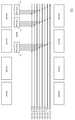
도 1은 종래기술에 따른 반도체 메모리 장치의 구성을 개략적으로 보여주는 도면이다. 도 1에서, 상기 반도체 메모리 장치(10)는 제 1 내지 제 8 메모리 뱅크(Bank0~Bank7), 복수개의 데이터 입출력 라인(GIO_0<0:15>~GIO_7<0:15>) 및 데이터 입출력부(11, 12, 13)를 포함한다. 상기 데이터 입출력부(11, 12, 13)는 패드(도시하지 않음.)와 연결되고, 상기 데이터 입출력부(11, 12, 13)와 상기 제 1 내지 제 8 메모리 뱅크(Bank0~Bank7)는 상기 데이터 입출력 라인(GIO_0<0:15>~GIO_7<0:15>)을 통해 서로 통신할 수 있다. 상기 데이터 입출력부(11, 12, 13)는 각각의 메모리 뱅크마다 다수개가 구비되며, 도 1에서, 설명의 편의상 상기 데이터 입출력부(11, 12, 13) 중 데이터의 입력, 즉, 라이트 동작과 연관된 데이터 정렬회로(Din) 및 데이터의 출력, 즉, 리드 동작과 연관된 파이프 래치회로(PIPE)만이 도시되어 있다.1 is a view schematically showing a configuration of a semiconductor memory device according to the prior art. In FIG. 1, the
상기 반도체 메모리 장치(10)의 라이트 동작에서, 외부에서 패드를 통해 입력된 직렬 데이터는 상기 데이터 입출력부(11, 12, 13)를 구성하는 데이터 정렬회로(Din)를 통해 병렬 데이터로 변환된 후, 상기 데이터 입출력 라인(GIO_0<0:15>~GIO_7<0:15>)을 통해 해당 메모리 뱅크로 전송되고, 해당 메모리 뱅크에 저장된다. 상기 반도체 메모리 장치(10)의 리드 동작에서, 해당 메모리 뱅크에 저장된 데이터는 상기 데이터 입출력 라인(GIO_0<0:15>~GIO_7<0:15>)을 통해 상기 데이터 입출력부(11, 12, 13)를 구성하는 파이프 래치회로(PIPE)로 전송된다. 상기 파이프 래치회로(PIPE)는 병렬로 전송된 데이터를 직렬 데이터로 변환하고, 변환된 데이터는 패드를 통해 외부로 출력된다.In the write operation of the
위와 같이, 데이터의 입력 및 출력, 즉, 라이트 및 리드 동작에서, 상기 데이터 입출력 라인(GIO_0<0:15>~GIO_7<0:15>)은 데이터가 전송되는 경로가 된다. 상기 데이터 입출력 라인(GIO_0<0:15>~GIO_7<0:15>)은 메모리 뱅크들(Bank0~Bank7) 사이의 주변 영역(Peripheral Region)에 배치된다. 반도체 메모리 장치의 처리 용량이 높아지면서, 상기 데이터 입출력 라인(GIO_0<0:15>~GIO_7<0:15>)의 수는 점점 늘어날 수 밖에 없다. 예를 들어, 도 1에 도시된 바와 같이, 반도체 메모리 장치(10)가 8번 연속으로 리드 또는 라이트 동작을 수행하면서 16비트의 데이터를 한번에 처리하기 위해서는 총 128개의 상기 데이터 입출력 라인(GIO_0<0:15>~GIO_7<0:15>)을 필요로 한다. 따라서, 한정된 면적의 주변 영역에 위와 같이 다수의 데이터 입출력 라인이 배치되면, 반도체 메모리 장치의 레이아웃 마진을 확보하기 매우 어렵다.As described above, in the data input and output, that is, the write and read operations, the data input / output lines GIO_0 <0:15> to GIO_7 <0:15> become paths through which data is transmitted. The data input / output lines GIO_0 <0:15> to GIO_7 <0:15> are disposed in a peripheral region between memory banks Bank0 to Bank7. As the processing capacity of the semiconductor memory device increases, the number of the data input / output lines GIO_0 <0:15> to GIO_7 <0:15> may increase. For example, as shown in FIG. 1, in order to process 16-bit data at a time while the
본 발명은 상기와 같은 문제점을 해결하기 위해서 데이터 입출력 라인의 수를 감소시키고, 레이아웃 마진을 확보할 수 있는 데이터 입출력 구조를 갖는 반도체 메모리 장치를 제공하는데 그 목적이 있다.SUMMARY OF THE INVENTION An object of the present invention is to provide a semiconductor memory device having a data input / output structure capable of reducing the number of data input / output lines and securing a layout margin in order to solve the above problems.
본 발명의 실시예에 따른 반도체 메모리 장치는 제 1 메모리 뱅크의 데이터를 전송하는 제 1 데이터 입출력 라인; 상기 제 1 메모리 뱅크의 데이터를 전송하는 제 2 데이터 입출력 라인; 입출력 모드에 따라 상기 제 1 데이터 입출력 라인으로부터 전송된 데이터를 정렬하여 출력하는 제 1 데이터 출력부; 및 입출력 모드 및 어드레스 신호에 따라 상기 제 1 및 제 2 데이터 입출력 라인으로부터 전송된 데이터 중 하나를 정렬하여 출력하는 제 2 데이터 출력부; 를 포함한다.In an embodiment, a semiconductor memory device may include a first data input / output line configured to transfer data of a first memory bank; A second data input / output line configured to transfer data of the first memory bank; A first data output unit for sorting and outputting data transmitted from the first data input / output line according to an input / output mode; And a second data output unit for sorting and outputting one of data transmitted from the first and second data input / output lines according to an input / output mode and an address signal. It includes.
본 발명의 다른 실시예에 따른 반도체 메모리 장치는 입출력 모드에 따라 입력 데이터를 정렬하여 제 1 데이터 입출력 라인으로 출력하는 제 1 데이터 입력부; 상기 입력 데이터를 정렬하고, 입출력 모드 및 어드레스 신호에 따라 정렬된 데이터를 상기 제 1 데이터 입출력 라인 및 제 2 데이터 입출력 라인 중 하나로 출력하는 제 2 데이터 입력부; 및 상기 제 1 및 제 2 데이터 입출력 라인을 통해 전송된 데이터가 저장되는 제 1 메모리 뱅크를 포함한다.In accordance with another aspect of the present invention, a semiconductor memory device may include: a first data input unit configured to sort input data according to an input / output mode and output the first data input / output line; A second data input unit for aligning the input data and outputting data aligned according to an input / output mode and an address signal to one of the first data input / output line and the second data input / output line; And a first memory bank in which data transmitted through the first and second data input / output lines are stored.
또한, 본 발명의 다른 실시예에 따른 반도체 메모리 장치는 제 1 메모리 뱅크의 업 뱅크 및 제 2 메모리 뱅크의 업 뱅크; 상기 제 1 메모리 뱅크의 다운 뱅크 및 상기 제 2 메모리 뱅크의 다운 뱅크; 상기 제 1 및 제 2 메모리 뱅크의 업 뱅크와 연결되는 제 1 데이터 입출력 라인; 상기 제 1 및 제 2 메모리 뱅크의 다운 뱅크와 연결되는 제 2 데이터 입출력 라인; 상기 제 1 데이터 입출력 라인을 통해 상기 제 1 및 제 2 메모리 뱅크의 업 뱅크와 통신하는 제 1 데이터 입출력부; 및 상기 제 1 및 제 2 데이터 입출력 라인을 통해 상기 제 1 및 제 2 메모리 뱅크의 업 뱅크 및 다운 뱅크와 통신하는 제 2 데이터 입출력부를 포함한다.In addition, a semiconductor memory device according to another embodiment of the present invention may include an up bank of a first memory bank and an up bank of a second memory bank; A down bank of the first memory bank and a down bank of the second memory bank; A first data input / output line connected to up banks of the first and second memory banks; A second data input / output line connected to down banks of the first and second memory banks; A first data input / output unit communicating with up banks of the first and second memory banks through the first data input / output line; And a second data input / output unit configured to communicate with up banks and down banks of the first and second memory banks through the first and second data input / output lines.
본 발명에 의하면, 데이터 입출력 구조를 개선하여 데이터 입출력 라인의 수를 감소시키고, 반도체 메모리 장치의 레이아웃 마진을 확보할 수 있다.According to the present invention, it is possible to improve the data input / output structure to reduce the number of data input / output lines and to secure the layout margin of the semiconductor memory device.
도 1은 종래기술에 따른 반도체 메모리 장치의 구성을 개략적으로 보여주는 도면,
도 2는 본 발명의 실시예에 따른 반도체 메모리 장치의 구성을 개략적으로 보여주는 도면,
도 3은 도 2의 제 1 데이터 입출력부의 구성을 개략적으로 보여주는 블록도,
도 4는 도 2의 제 2 데이터 입출력부의 구성을 개략적으로 보여주는 블록도이다.1 is a view schematically showing a configuration of a semiconductor memory device according to the prior art;
2 is a view schematically showing a configuration of a semiconductor memory device according to an embodiment of the present invention;
3 is a block diagram schematically illustrating a configuration of a first data input / output unit of FIG. 2;
4 is a block diagram schematically illustrating a configuration of a second data input / output unit of FIG. 2.
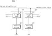
도 2는 본 발명의 실시예에 따른 반도체 메모리 장치의 구성을 개략적으로 보여주는 도면이다. 도 2에서, 상기 반도체 메모리 장치(1)는 제 1 내지 제 4 메모리 뱅크(Bank0~Bank3)를 포함한다. 상기 제 1 내지 제 4 메모리 뱅크(Bank0~Bank3)는 각각 업 뱅크(Bank0_up~Bank3_up) 및 다운 뱅크(Bank0_dn~Bank3_dn)로 구분되고, 상기 업 뱅크(Bank0_up~Bank3_up) 및 다운 뱅크(Bank0_dn~Bank3_dn)가 각각 다른 영역에 배치된다. 상기 제 1 메모리 뱅크의 업 뱅크(Bank0_up)와 상기 제 2 메모리 뱅크의 업 뱅크(Bank1_up)는 제 1 뱅크 영역(A)에 배치될 수 있고, 상기 제 1 메모리 뱅크의 다운 뱅크(Bank0_dn)와 상기 제 2 메모리 뱅크의 다운 뱅크(Bank1_dn)는 제 2 뱅크 영역(B)에 배치될 수 있다. 마찬가지로, 상기 제 3 메모리 뱅크의 업 뱅크(Bank2_up) 및 상기 제 4 메모리 뱅크의 업 뱅크(Bank3_up)는 제 3 뱅크 영역(C)에 배치될 수 있고, 상기 제 3 메모리 뱅크의 다운 뱅크(Bank2_dn) 및 상기 제 4 메모리 뱅크의 다운 뱅크(Bank3_dn)는 제 4 뱅크 영역(D)에 배치될 수 있다. 도 2에서, 상기 제 1 및 제 3 뱅크 영역(A, C)은 좌측에 배치되고, 상기 제 2 및 제 4 뱅크 영역(B, D)은 우측에 배치한다.2 is a diagram schematically illustrating a configuration of a semiconductor memory device according to an embodiment of the present invention. In FIG. 2, the
도 2에서, 상기 반도체 메모리 장치(1)는 제 1 데이터 입출력 라인(GIO_0<8:15>~GIO_7<8:15>), 제 2 데이터 입출력 라인(GIO_0<0:7>~GIO_7<0:7>), 제 1 데이터 입출력부(100) 및 제 2 데이터 입출력부(200)를 포함한다. 상기 제 1 데이터 입출력 라인(GIO_0<8:15>~GIO_7<8:15>)은 상기 제 1 내지 제 4 메모리 뱅크의 업 뱅크(Bank0_up~Bank3_up)들과 연결된다. 즉, 상기 제 1 및 제 2 데이터 입출력부(100, 200)를 기준으로 좌측으로 연장되어 배치된다. 상기 제 2 데이터 입출력 라인(GIO_0<0:7>~GIO_7<0:7>)은 상기 제 1 내지 제 4 메모리 뱅크의 다운 뱅크(Bank0_dn~Bank7_dn)들과 연결된다. 즉, 상기 제 1 및 제 2 데이터 입출력부(100, 200)를 기준으로 우측으로 연장되어 배치된다.In FIG. 2, the
상기 제 1 데이터 입출력부(100)는 상기 제 1 데이터 입출력 라인(GIO_0<8:15>~GIO_7<8:15>)과 연결된다. 상기 반도체 메모리 장치(1)의 리드 동작에서, 상기 제 1 내지 제 4 메모리 뱅크의 업 뱅크(Bank0_up~Bank3_up)에 저장된 데이터는 상기 제 1 데이터 입출력 라인(GIO_0<8:15>~GIO_7<8:15>)을 통해 상기 제 1 데이터 입출력부(100)로 전송되어 정렬된다. 또한, 상기 반도체 장치(1)의 라이트 동작에서, 입력된 데이터는 상기 제 1 데이터 입출력부(100)를 통해 정렬되고, 정렬된 데이터는 상기 제 1 데이터 입출력 라인(GIO_0<8:15>~GIO_7<8:15>)을 통해 상기 제 1 내지 제 4 메모리 뱅크의 업 뱅크들(Bank0_up~Bank3_up)로 전송될 수 있다. 따라서, 상기 제 1 데이터 입출력부(100)는 상기 제 1 데이터 입출력 라인(GIO_0<8:15>~GIO_7<8:15>)을 통해 상기 제 1 내지 제 4 메모리 뱅크의 업 뱅크들(Bank0_up~Bank3_up)과 통신할 수 있다.The first data input /
상기 제 1 데이터 입출력부(100)는 입출력 모드에 따라 상기 제 1 데이터 입출력 라인(GIO_0<8:15>~GIO_7<8:15>)과 선택적으로 연결된다. 따라서, 상기 제 1 데이터 입출력부(100)는 상기 입출력 모드에 따라 상기 제 1 내지 제 4 메모리 뱅크의 업 뱅크(Bank0_up~Bank3_up)와 선택적으로 통신할 수 있다. 예를 들어, 상기 제 1 데이터 입출력부(100)는 제 1 입출력 모드에서 상기 제 1 데이터 입출력 라인(GIO_0<8:15>~GIO_7<8:15>)과 연결되지 않고, 제 2 입출력 모드에서 상기 제 1 데이터 입출력 라인(GIO_0<8:15>~GIO_7<8:15>)과 연결될 수 있다. 따라서, 상기 제 1 데이터 입출력부(100)는 상기 제 1 입출력 모드에서 비활성화된다.The first data input /
상기 제 2 데이터 입출력부(200)는 상기 제 1 및 제 2 데이터 입출력 라인(GIO_0<8:15>~GIO_7<8:15>, GIO_0<0:7>~GIO_7<0:7>)과 연결된다. 상기 제 2 데이터 입출력부(200)는 입출력 모드 및 어드레스 신호(ADD)에 따라 상기 제 1 및 제 2 데이터 입출력 라인(GIO_0<8:15>~GIO_7<8:15>, GIO_0<0:7>~GIO_7<0:7>) 중 하나와 선택적으로 통신할 수 있다. 상기 제 2 데이터 입출력부(200)는 제 1 입출력 모드에서 상기 어드레스 신호(ADD)에 응답하여 상기 제 1 및 제 2 데이터 입출력 라인(GIO_0<8:15>~GIO_7<8:15>, GIO_0<0:7>~GIO_7<0:7>) 중 하나와 통신하고, 제 2 입출력 모드에서 상기 제 2 데이터 입출력 라인(GIO_0<0:7>~GIO_7<0:7>)과 통신한다. 제 1 입출력 모드에서, 상기 제 2 데이터 입출력부(200)는 리드 동작 중에 상기 어드레스 신호(ADD)에 응답하여 상기 제 1 및 제 2 데이터 입출력 라인(GIO_0<8:15>~GIO_7<8:15>, GIO_0<0:7>~GIO_7<0:7>) 중 하나와 연결되고, 상기 연결된 데이터 입출력 라인으로부터 전송된 데이터를 정렬하여 출력한다. 제 1 입출력 모드에서, 상기 제 2 데이터 입출력부(200)는 라이트 동작 중에 입력 데이터를 정렬하고, 상기 어드레스 신호(ADD)에 응답하여 상기 정렬된 데이터를 상기 제 1 및 제 2 데이터 입출력 라인(GIO_0<8:15>~GIO_7<8:15>, GIO_0<0:7>~GIO_7<0:7>) 중 하나로 전송한다. 제 2 입출력 모드에서, 상기 제 2 데이터 입출력부(200)는 리드 동작 중에 상기 제 2 데이터 입출력 라인(GIO_0<0:7>~GIO_7<0:7>)을 통해 전송된 데이터를 정렬하여 출력하고, 라이트 동작 중에 입력 데이터를 정렬하고 정렬된 데이터를 상기 제 2 데이터 입출력 라인(GIO_0<0:7>~GIO_7<0:7>)으로 출력한다. 따라서, 상기 제 2 데이터 입출력부(200)는 제 1 입출력 모드에서 상기 어드레스 신호(ADD)에 따라 상기 제 1 내지 제 4 메모리 뱅크의 업 뱅크들(Bank0_up~Bank3_up) 및 상기 제 1 내지 제 4 메모리 뱅크의 다운 뱅크들(Bank0_dn~Bank3_dn) 중 하나와 선택적으로 통신할 수 있으며, 제 2 입출력 모드에서 상기 제 1 내지 제 4 메모리 뱅크의 다운 뱅크들(Bank0_dn~Bank3_dn)과 통신할 수 있다.The second data input /
상기 제 1 및 제 2 입출력 모드는 입출력 모드신호(I/O)에 의해 지정될 수 있다. 상기 입출력 모드신호(I/O)는 상기 반도체 메모리 장치(1)가 한 번에 입출력할 수 있는 데이터의 수를 지정하는 신호로서, 일반적으로 X4, X8 및 X16 신호가 사용된다. X4 신호는 한 번에 4비트의 데이터가 입출력될 수 있는 입출력 모드를 나타내고, X8 신호는 한 번에 8비트의 데이터가 입출력될 수 있는 입출력 모드를 나타내며, X16 모드는 한 번에 16 비트의 데이터가 입출력될 수 있는 입출력 모드를 나타낸다. 상기 입출력 모드신호(I/O)는 반도체 메모리 장치의 모드 레지스터 셋(Mode Register Set)에서 생성될 수 있다. 본 발명의 실시예에서, 상기 제 1 입출력 모드는 X8 신호에 의해 지정되는 입출력 모드이고, 상기 제 2 입출력 모드는 X16 신호에 의해 지정되는 입출력 모드일 수 있지만, 이에 한정하는 것은 아니다. 상기 어드레스 신호(ADD)는 일반적으로 반도체 메모리 장치의 열 선택에 이용되는 로우 어드레스 신호(Row Address Signal) 중 하나를 이용할 수 있다.The first and second input / output modes may be designated by an input / output mode signal I / O. The input / output mode signal I / O is a signal that specifies the number of data that the
상기 반도체 메모리 장치(1)는 제 1 내지 제 4 메모리 뱅크(Bank0~Bank3)를 업 뱅크(Bank0_up~Bank3_up)와 다운 뱅크(Bank0_dn~Bank3_dn)로 분할하여 각각 제 1 내지 제 4 뱅크 영역(A~D)에 위치시키고, 상기 제 1 내지 제 4 뱅크 영역(A~D)을 좌측과 우측에 배치시킨다. 상기 제 1 및 제 2 데이터 입출력부(100, 200)는 상기 제 1 내지 제 4 뱅크 영역(A~D)의 사이, 즉, 상기 주변 영역의 중앙에 위치한다. 좌측에 배치되는 제 1 내지 제 4 메모리 뱅크의 업 뱅크들(Bank0_up~Bank3_up)은 상기 제 1 데이터 입출력 라인(GIO_0<8:15>~GID_7<8:15>)을 통해 상기 제 1 데이터 입출력부(100)와 연결된다. 또한, 우측에 배치되는 제 1 내지 제 4 메모리 뱅크의 다운 뱅크들(Bank0_dn~Bank3_dn)은 상기 제 2 데이터 입출력 라인(GIO_0<0:7>~GIO_7<0:7>)을 통해 상기 제 2 데이터 입출력부(200)와 연결된다. 위와 같은 구조 및 배치를 통해, 하나의 메모리 뱅크에 128개의 데이터 입출력 라인이 배치되던 종래기술과 달리 그 절반인 64개의 데이터 입출력 라인이 배치되어도 종래와 동일하세 반도체 메모리 장치의 데이터 입출력 동작이 수행될 수 있다.The
도 2에서, 상기 반도체 메모리 장치(1)는 데이터 입출력 버퍼부(300)를 더 포함할 수 있다. 상기 데이터 입출력 버퍼부(300)는 리드 동작에서 상기 제 1 및 제 2 데이터 입출력부(100, 200)에서 출력된 데이터를 버퍼링하여 패드(도시하지 않음.)로 출력한다. 상기 데이터 입출력 버퍼부(300)는 라이트 동작에서 상기 패드를 통해 입력된 외부 데이터를 버퍼링하여 상기 제 1 및 제 2 입출력부(100, 200)로 전송한다. 상기 데이터 입출력 버퍼부(300)는 상기 제 1 및 제 2 데이터 입출력부(100, 200)와 다르게, 뱅크 영역(A~D)에 인접하여 배치될 수 있다. 즉, 상기 데이터 입출력 버퍼부(300)는 종래기술과 동일하게 패드가 위치하는 부분에 배치된다.In FIG. 2, the
도 3은 도 2의 제 1 데이터 입출력부의 구성을 개략적으로 보여주는 블록도이다. 도 3에서, 상기 제 1 데이터 입출력부(100)는 제 1 데이터 출력부(110) 및 제 1 데이터 입력부(120)를 포함한다. 상기 제 1 데이터 출력부(110) 및 상기 제 1 데이터 입력부(120)는 상기 입출력 모드에 따라 상기 제 1 데이터 입출력 라인(GIO_0<8:15>~GIO_7<8:15>)과 선택적으로 연결된다. 상기 제 1 데이터 출력부(110) 및 상기 제 1 데이터 입력부(120)는 입출력 모드신호(I/O)에 의해 지정되는 제 1 입출력 모드에서 상기 제 1 데이터 입출력 라인(GIO_0<8:15>~GIO_7<8:15>)과 연결되지 않으며, 상기 입출력 모드신호(I/O)에 의해 지정되는 제 2 입출력 모드에서 상기 제 1 데이터 입출력 라인(GIO_0<8:15>~GIO_7<8:15>)과 연결된다.3 is a block diagram schematically illustrating a configuration of a first data input / output unit of FIG. 2. In FIG. 3, the first data input /
상기 제 1 데이터 출력부(110)는 제 1 출력 선택부(111) 및 제 1 파이프 래치회로(112)를 포함한다. 상기 제 1 출력 선택부(111)는 입출력 모드에 따라 상기 제 1 데이터 입출력 라인(GIO_0<8:15>~GIO_7<8:15>)을 통해 전송되는 데이터를 출력한다. 상기 제 1 파이프 래치회로(112)는 상기 제 1 출력 선택부(111)로부터 출력된 데이터를 정렬하고, 정렬된 데이터를 상기 데이터 입출력 버퍼부(300)로 출력한다. 따라서, 상기 제 1 데이터 출력부(110)는 상기 반도체 메모리 장치(1)의 리드 동작과 관련되는 회로이다. 상기 제 1 출력 선택부(110)는 상기 입출력 모드신호(I/O)를 제어신호로 하는 멀티플렉서로 구현될 수 있고, 상기 제 1 파이프 래치회로(112)는 종래기술을 이용할 수 있다.The first
상기 제 1 데이터 입력부(120)는 제 1 입력 선택부(121) 및 제 1 데이터 정렬회로(122)를 포함한다. 상기 제 1 입력 선택부(121)는 입출력 모드에 따라 상기 제 1 데이터 입출력 라인(GIO_0<8:15>~GIO_7<8:15>)과 선택적으로 연결된다. 상기 제 1 데이터 정렬회로(122)는 상기 데이터 입출력 버퍼부(300)로부터 입력된 데이터를 정렬하고, 정렬된 데이터를 상기 제 1 입력 선택부(121)로 출력한다. 따라서, 상기 제 1 데이터 입력부(120)는 상기 반도체 메모리 장치(1)의 라이트 동작과 관련되는 회로이다. 상기 제 1 입력 선택부(120)는 상기 입출력 모드신호(I/O)를 제어신호로 하는 멀티플렉서로 구현될 수 있고, 상기 제 1 데이터 정렬회로(122)는 종래기술과 동일하다.The first
위와 같은 구성을 통해, 상기 제 1 데이터 입출력부(100)는 입출력 모드에 따라 상기 제 1 데이터 입출력 라인(GIO_0<8:15>~GIO_7<8:15>)과 선택적으로 연결되어 상기 제 1 내지 제 4 메모리 뱅크의 업 뱅크들(Bank0_up~Bank3_up)과 통신할 수 있다. 즉, 상기 제 1 데이터 입출력부(100)는 상기 제 2 입출력 모드에서 상기 제 1 내지 제 4 메모리 뱅크의 업 뱅크들(Bank0_up~Bank3_up)의 리드/라이트 동작을 수행할 수 있다.Through the above configuration, the first data input /
도 4는 도 2의 제 2 데이터 입출력부의 구성을 개략적으로 보여주는 도면이다. 도 3에서, 상기 제 2 데이터 입출력부(200)는 제 데이터 출력부(210) 및 제 2 데이터 입력부(220)를 포함한다. 상기 제 2 데이터 출력부(210) 및 상기 제 2 데이터 입력부(220)는 입출력 모드 및 어드레스 신호(ADD)에 따라 상기 제 1 및 제 2 데이터 입출력 라인(GIO_0<8:15>~GIO_7<8:15>, GIO_0<0:7>~GIO_7<0:7>) 중 하나와 연결된다.4 is a diagram schematically illustrating a configuration of a second data input / output unit of FIG. 2. In FIG. 3, the second data input /
상기 제 2 데이터 출력부(210)는 제 2 출력 선택부(211) 및 제 2 파이프 래치회로(212)를 포함한다. 상기 제 2 데이터 입력부(220)는 제 2 입력 선택부(221) 및 제 2 데이터 정렬회로(222)를 포함한다. 따라서, 상기 제 2 데이터 출력부(210)는 상기 반도체 메모리 장치(1)의 리드 동작과 관련되는 회로이고, 상기 제 2 데이터 입력부(220)는 상기 반도체 메모리 장치(1)의 라이트 동작과 관련되는 회로이다. 상기 제 2 출력 선택부(211) 및 상기 제 2 입력 선택부(221)는 각각 입출력 모드신호(I/O) 및 어드레스 신호(ADD)를 제어신호로 하는 멀티플렉서로 구현할 수 있고, 상기 제 2 파이프 래치회로(212) 및 제 2 데이터 정렬회로(222)는 종래기술과 동일하다.The second
상기 반도체 메모리 장치(1)의 리드 동작을 먼저 살펴보면, 상기 제 2 출력 선택부(211)는 상기 입출력 모드 및 상기 어드레스 신호(ADD)에 따라 상기 제 1 및 제 2 데이터 입출력 라인(GIO_0<8:15>~GIO_7<8:15>, GIO_0<0:7>~GIO_7<0:7>) 중 하나와 연결된다. 상기 입출력 모드신호(I/O)에 의해 지정되는 상기 제 1 입출력 모드에서 상기 제 2 출력 선택부(211)는 상기 어드레스 신호(ADD)에 따라 상기 제 1 및 제 2 데이터 입출력 라인(GIO_0<8:15>~GIO_7<8:15>, GIO_0<0:7>~GIO_7<0:7>) 중 하나로부터 전송된 데이터를 출력한다. 상기 입출력 모드신호(I/O)에 의해 지정되는 제 2 입출력 모드에서 상기 제 2 출력 선택부(211)는 상기 어드레스 신호(ADD)에 무관하게 상기 제 2 데이터 입출력 라인(GIO_0<0:7>~GIO_7<0:7>)으로부터 전송된 데이터를 출력한다. 상기 제 2 출력 선택부(211)를 통해 출력된 데이터는 상기 제 2 파이프 래치회로(212)에 의해 정렬되고, 정렬된 데이터는 데이터 입출력 버퍼부(300)로 출력된다.Referring to the read operation of the
상기 반도체 메모리 장치(1)의 라이트 동작을 살펴보면. 상기 데이터 입출력 버퍼부(300)를 통해 입력된 데이터는 상기 제 2 데이터 정렬회로(222)에 의해 정렬되고 상기 제 2 입력 선택부(221)로 입력된다. 상기 제 2 입력 선택부(221)는 상기 입출력 모드 및 상기 어드레스 신호(ADD)에 따라 상기 제 1 및 제 2 데이터 입출력 라인(GIO_0<8:15>~GIO_7<8:15>, GIO_0<0:7>~GIO_7<0:7>) 중 하나와 연결된다. 상기 입출력 모드신호(I/O)에 의해 지정되는 상기 제 1 입출력 모드에서 상기 제 2 입력 선택부(221)는 상기 어드레스 신호(ADD)에 따라 상기 제 1 및 제 2 데이터 입출력 라인(GIO_0<8:15>~GIO_7<8:15>, GIO_0<0:7>~GIO_7<0:7>)과 선택적으로 연결된다. 예를 들어, 상기 어드레스 신호(ADD)가 하이 레벨인 경우 상기 제 2 입력 선택부(221)는 상기 제 1 데이터 입출력 라인(GIO_0<8:15>~GIO_7<8:15>)과 연결되고, 상기 제 2 데이터 정렬부(222)에 의해 정렬된 데이터는 상기 제 1 데이터 입출력 라인(GIO_0<8:15>~GIO_7<8:15>)을 통해 상기 제 1 내지 제 4 메모리 뱅크의 업 뱅크(Bank0_up~Bank3_up)로 전송될 수 있다. 반대로, 상기 어드레스 신호(ADD)가 로우 레벨인 경우, 상기 제 2 입력 선택부(221)는 상기 제 2 데이터 입출력 라인(GIO_0<0:7>~GIO_7<0:7>)과 연결되고, 상기 제 2 데이터 정렬회로(222)에 의해 정렬된 데이터는 상기 제 2 데이터 입출력 라인(GIO_0<0:7>~GIO_7<0:7>)을 통해 상기 제 1 내지 제 4 메모리 뱅크의 다운 뱅크(Bank0_dn~Bank3_dn)로 전송될 수 있다. 상기 제 2 입출력 모드에서, 상기 제 2 입력 선택부(221)는 상기 어드레스 신호(ADD)에 무관하게 상기 제 2 데이터 정렬회로(222)에 의해 정렬된 데이터를 상기 제 2 데이터 입출력 라인(GIO_0<0:7>~GIO_7<0:7>)으로 전송한다.A write operation of the
도 2 내지 도 4를 참조하여, 본 발명의 실시예에 따른 반도체 메모리 장치의 구체적인 동작을 살펴보면 다음과 같다. 제 1 입출력 모드에서 상기 반도체 메모리 장치(1)의 리드 동작을 먼저 설명한다. 제 1 메모리 뱅크의 업 뱅크(Bank0_up)의 리드 동작이 수행되는 경우, 상기 어드레스 신호(ADD)가 하이 레벨이 된다. 상기 제 1 데이터 입출력부(100)는 비활성화되고, 상기 제 2 데이터 출력부(210)의 제 2 출력 선택부(211)는 제 1 데이터 입출력 라인(GIO_0<8:15>~GIO_7<8:15>)과 연결된다. 상기 제 1 메모리 뱅크의 업 뱅크(Bank0_up)에 저장된 데이터는 상기 제 1 데이터 입출력 라인(GIO_0<8:15>~GIO_7<8:15>)으로 전송되고, 상기 제 1 데이터 입출력 라인(GIO_0<8:15>~GIO_7<8:15>)으로 전송된 데이터는 상기 제 2 출력 선택부(211)를 통해 상기 제 2 파이프 래치회로(212)로 입력된다. 상기 파이프 래치회로(212)는 병렬로 입력되는 데이터를 정렬하여 직렬 데이터로 출력한다. 상기 데이터 입출력 버퍼부(300)는 상기 정렬된 직렬 데이터를 버퍼링하고, 버퍼링된 데이터는 패드를 통해 외부로 출력될 수 있다. 위와 반대로, 제 1 메모리 뱅크의 다운 뱅크(Bank0_dn)의 리드 동작이 수행되는 경우, 상기 어드레스 신호(ADD)는 로우 레벨이되고, 상기 제 2 출력 선택부(211)는 상기 제 2 데이터 입출력 라인(GIO_0<0:7>~GIO_7<0:7>)과 연결되므로, 상기 제 1 메모리 뱅크의 다운 뱅크(Bank0_dn)에 저장된 데이터가 상기 제 2 파이프 래치회로(212)로 입력된다. 따라서, 상기 제 2 파이프 래치회로(212) 및 상기 데이터 입출력 버퍼부(300)를 통해 상기 제 1 메모리 뱅크의 다운 뱅크(Bank0_dn)에 저장된 데이터가 출력될 수 있다. 따라서, 제 1 입출력 모드에서 입출력되는 데이터의 비트 수는 상기 제 2 입출력 모드에서 입출력되는 데이터의 비트 수의 절반이므로, 상기 제 1 입출력 모드에서는 상기 제 2 데이터 입출력부(200)를 통해 상기 반도체 메모리 장치(1)의 리드/라이트 동작이 수행된다.2 to 4, a detailed operation of a semiconductor memory device according to an embodiment of the present invention will be described. First, the read operation of the
상기 제 1 메모리 뱅크의 업 뱅크(Bank0_up)의 라이트 동작이 수행되는 경우, 상기 패드 및 데이터 입출력 버퍼부(300)를 통해 외부로부터 입력된 데이터는 제 2 데이터 입출력부(200)의 제 2 데이터 정렬회로(222)로 입력되어 정렬된다. 상기 정렬된 데이터는 상기 제 2 데이터 입력부(220)의 제 2 입력 선택부(221)로 입력된다. 이때, 상기 어드레스 신호(ADD)가 하이 레벨이므로, 상기 제 2 입력 선택부(221)는 상기 제 1 데이터 입출력 라인(GIO_0<8:15>~GIO_7<8:15>)과 연결되고, 상기 정렬된 데이터는 상기 제 1 데이터 입출력 라인(GIO_0<8:15>~GIO_7<8:15>)을 통해 상기 제 1 메모리 뱅크의 업 뱅크(Bank0_up)로 전송되어, 상기 제 1 메모리 뱅크의 업 뱅크(Bank0_up)에 저장된다.When a write operation of the up bank Bank0_up of the first memory bank is performed, data input from the outside through the pad and the data input /
상기 제 1 메모리 뱅크의 다운 뱅크(Bank0_dn)의 라이트 동작이 수행되는 경우, 상기 어드레스 신호(ADD)는 로우 레벨이 된다. 상기 제 2 입력 선택부(221)는 상기 제 2 데이터 입출력 라인(GIO_0<0:7>~GIO_7<0:7>)과 연결되고, 상기 제 2 데이터 정렬회로(222)에 의해 정렬된 데이터는 상기 제 2 데이터 입출력 라인(GIO_0<0:7>~GIO_7<0:7>)을 통해 상기 제 1 메모리 뱅크의 다운 뱅크(Bank0_dn)로 전송되어, 상기 제 1 메모리 뱅크의 다운 뱅크(Bank0_dn)에 저장될 수 있다.When the write operation of the down bank Bank0_dn of the first memory bank is performed, the address signal ADD is at a low level. The
제 2 입출력 모드에서 상기 제 1 데이터 입출력부의 제 1 출력 선택부(111)는 및 제 1 입력 선택부(121)는 상기 제 1 데이터 입출력 라인(GIO_0<8:15>~GIO_7<8:15>)과 연결되고, 상기 제 2 데이터 입출력부(200)의 상기 제 2 출력 선택부(211) 및 제 2 입력 선택부(221)는 상기 어드레스 신호(ADD)에 무관하게 상기 제 2 데이터 입출력 라인(GIO_0<0:7>~GIO_7<0:7>)과 연결된다.In the second input / output mode, the
리드 동작시, 상기 제 1 메모리 뱅크의 업 뱅크(Bank0_up)에 저장된 데이터는 상기 제 1 데이터 입출력 라인(GIO_0<8:15>~GIO_7<8:15>)으로 전송되고, 상기 제 1 메모리 뱅크의 다운 뱅크(Bank0_dn)에 저장된 데이터는 상기 제 2 데이터 입출력 라인(GIO_0<0:7>~GIO_7<0:7>)으로 전송된다. 상기 제 1 데이터 출력부(110)의 제 1 출력 선택부(111)는 상기 제 1 데이터 입출력 라인(GIO_0<8:15>~GIO_7<8:15>)을 통해 전송된 데이터를 상기 제 1 파이프 래치회로(112)로 출력하고, 상기 제 2 데이터 출력부(210)의 제 2 출력 선택부(211)는 상기 제 2 데이터 입출력 라인(GIO_0<0:7>~GIO_7<0:7>)을 통해 전송된 데이터를 상기 제 2 파이프 래치회로(212)로 출력한다. 상기 제 1 및 제 2 파이프 래치회로(112, 212)는 각각 상기 제 1 및 제 2 출력 선택부(111, 211)로부터 출력된 데이터를 정렬하고, 정렬된 데이터를 상기 데이터 입출력 버퍼부(300)로 출력한다. 상기 데이터 입출력 버퍼부(300)는 상기 정렬된 데이터를 버퍼링하여 상기 패드를 통해 출력함으로써, 상기 제 1 메모리 뱅크의 업 뱅크 및 다운 뱅크(Bank0_up, Bank0_dn)의 리드 동작이 수행될 수 있다. 상기 제 2 내지 제 4 메모리 뱅크(Bank1~Bank3)의 리드 동작도 동일하게 수행될 수 있다.In a read operation, data stored in the up bank Bank0_up of the first memory bank is transferred to the first data input / output lines GIO_0 <8:15> to GIO_7 <8:15>, and Data stored in the down bank Bank0_dn is transferred to the second data input / output lines GIO_0 <0: 7> to GIO_7 <0: 7>. The
라이트 동작시, 상기 패드 및 상기 데이터 입출력 버퍼부(300)를 통해 입력된 외부 데이터는 상기 제 1 및 제 2 데이터 정렬회로(122, 222)로 입력된다. 상기 제 1 및 제 2 데이터 정렬회로(122, 222)는 입력된 데이터를 정렬하고, 상기 제 1 및 제 2 입력 선택부(121, 221)로 출력한다. 상기 제 1 입력 선택부(121)는 상기 제 1 데이터 입출력 라인(GIO_0<8:15>~GIO_7<8:15>)과 연결되므로, 상기 제 1 데이터 정렬회로(122)에 의해 정렬된 데이터는 상기 제 1 데이터 입출력 라인(GIO_0<8:15>~GIO_7<8:15>)을 통해 전송되고, 상기 제 1 메모리 뱅크의 업 뱅크(Bank0_up)에 저장될 수 있다, 상기 제 2 입력 선택부(221)는 상기 제 2 데이터 입출력 라인(GIO_0<0:7>~GIO_7<0:7>)과 연결되므로, 상기 제 2 데이터 정렬회로(222)에 의해 정렬된 데이터는 상기 제 2 데이터 입출력 라인(GIO_0<0:7>~GIO_7<0:7>)을 통해 전송되고, 상기 제 1 메모리 뱅크의 다운 뱅크(Bank0_dn)에 저장될 수 있다. 따라서, 상기 제 1 메모리 뱅크의 업 뱅크 및 다운 뱅크(Bank0_up, Bank0_dn)의 라이트 동작이 수행될 수 있다. 상기 제 2 내지 제 4 메모리 뱅크(Bank1~Bank3)의 라이트 동작도 동일하게 수행될 수 있다.In the write operation, external data input through the pad and the data input /
따라서, 본 발명은 메모리 뱅크를 업 뱅크와 다운 뱅크로 분할 배치하고, 분할된 메모리 뱅크의 데이터 입출력 동작을 수행하는 데이터 입출력부를 주변 영역 중앙에 배치함으로써, 종래보다 데이터 입출력 라인의 수를 감소시킬 수 있다. 따라서, 반도체 메모리 장치의 레이아웃 마진을 개선할 수 있다. 또한, 입출력 모드에 따라 감소된 데이터 입출력 라인을 선택적으로 활용할 수 있는 데이터 입출력 구조를 갖고 있다.Accordingly, the present invention can reduce the number of data input / output lines by conventionally arranging a memory bank into an up bank and a down bank and arranging a data input / output unit for performing data input / output operations of the divided memory bank in the center of the peripheral region. have. Therefore, the layout margin of the semiconductor memory device can be improved. In addition, it has a data input / output structure that can selectively utilize the reduced data input / output lines according to the input / output mode.
본 발명이 속하는 기술분야의 당업자는 본 발명이 그 기술적 사상이나 필수적 특징을 변경하지 않고서 다른 구체적인 형태로 실시될 수 있으므로, 이상에서 기술한 실시예들은 모든 면에서 예시적인 것이며 한정적인 것이 아닌 것으로서 이해해야만 한다. 본 발명의 범위는 상기 상세한 설명보다는 후술하는 특허청구범위에 의하여 나타내어지며, 특허청구범위의 의미 및 범위 그리고 그 등가개념으로부터 도출되는 모든 변경 또는 변형된 형태가 본 발명의 범위에 포함되는 것으로 해석되어야 한다.As those skilled in the art to which the present invention pertains may implement the present invention in other specific forms without changing the technical spirit or essential features, the embodiments described above should be understood as illustrative and not restrictive in all aspects. Should be. The scope of the present invention is shown by the following claims rather than the detailed description, and all changes or modifications derived from the meaning and scope of the claims and their equivalents should be construed as being included in the scope of the present invention. do.
100: 제 1 데이터 입출력부200: 제 2 데이터 입출력부
300: 데이터 입출력 버퍼링부100: first data input / output unit 200: second data input / output unit
300: data input / output buffering unit
Claims (21)
Translated fromKorean상기 제 1 메모리 뱅크의 데이터를 전송하는 제 2 데이터 입출력 라인;
입출력 모드에 따라 상기 제 1 데이터 입출력 라인으로부터 전송된 데이터를 정렬하여 출력하는 제 1 데이터 출력부; 및
입출력 모드 및 어드레스 신호에 따라 상기 제 1 및 제 2 데이터 입출력 라인으로부터 전송된 데이터 중 하나를 정렬하여 출력하는 제 2 데이터 출력부를 포함하는 반도체 메모리 장치.A first data input / output line for transferring data of the first memory bank;
A second data input / output line configured to transfer data of the first memory bank;
A first data output unit for sorting and outputting data transmitted from the first data input / output line according to an input / output mode; And
And a second data output unit arranged to output one of the data transmitted from the first and second data input / output lines according to an input / output mode and an address signal.
상기 제 1 데이터 출력부는, 제 1 입출력 모드에서 비활성화되고, 제 2 입출력 모드에서 상기 제 1 데이터 입출력 라인으로부터 전송된 데이터를 정렬하여 출력하는 것을 특징으로 하는 반도체 메모리 장치.The method of claim 1,
And the first data output unit is inactivated in a first input / output mode and sorts and outputs data transmitted from the first data input / output line in a second input / output mode.
상기 제 2 데이터 출력부는, 상기 제 1 입출력 모드에서 상기 제 2 데이터 입출력 라인으로부터 전송된 데이터를 정렬하여 출력하고, 상기 제 2 입출력 모드에서 상기 어드레스 신호에 따라 상기 제 1 및 제 2 데이터 입출력 라인 중 하나로부터 전송된 데이터를 정렬하여 출력하는 것을 특징으로 하는 반도체 메모리 장치.The method of claim 2,
The second data output unit aligns and outputs data transmitted from the second data input / output line in the first input / output mode, and among the first and second data input / output lines according to the address signal in the second input / output mode. And sorting and outputting data transmitted from one.
상기 제 1 데이터 출력부는, 상기 입출력 모드에 따라 상기 제 1 데이터 입출력 라인과 선택적으로 연결되는 제 1 출력 선택부; 및
상기 제 1 출력 선택부로부터 출력된 데이터를 정렬하는 제 1 파이프 래치회로로 구성되는 것을 특징으로 하는 반도체 메모리 장치.The method of claim 1,
The first data output unit may include: a first output selector selectively connected to the first data input / output line according to the input / output mode; And
And a first pipe latch circuit for aligning data output from the first output selector.
상기 제 2 데이터 출력부는, 상기 입출력 모드 및 상기 어드레스 신호에 따라 상기 제 1 및 제 2 데이터 입출력 라인과 선택적으로 연결되는 제 2 출력 선택부; 및
상기 제 2 출력 선택부로부터 출력된 데이터를 정렬하는 제 2 파이프 래치회로로 구성되는 것을 특징으로 하는 반도체 메모리 장치.The method of claim 4, wherein
The second data output unit may include: a second output selector selectively connected to the first and second data input / output lines according to the input / output mode and the address signal; And
And a second pipe latch circuit for aligning data output from the second output selector.
상기 제 1 데이터 출력부는, 상기 제 1 데이터 입출력 라인을 통해 병렬로 전송된 데이터를 직렬 데이터로 정렬하여 출력하는 것을 특징으로 하는 반도체 메모리 장치.The method of claim 1,
And the first data output unit aligns and outputs data transmitted in parallel through the first data input / output line into serial data.
상기 제 2 데이터 출력부는, 상기 제 1 및 제 2 데이터 입출력 라인을 통해 병렬로 전송된 데이터를 직렬 데이터로 정렬하여 출력하는 것을 특징으로 하는 반도체 메모리 장치.The method of claim 1,
And the second data output unit aligns and outputs data transmitted in parallel through the first and second data input / output lines into serial data.
상기 제 1 및 제 2 데이터 출력부로부터 출력된 데이터를 버퍼링하여 패드로 출력하는 데이터 출력 버퍼부를 더 포함하는 것을 특징으로 하는 반도체 메모리 장치.The method of claim 1,
And a data output buffer unit configured to buffer data output from the first and second data output units and output the buffered data to a pad.
상기 입력 데이터를 정렬하고, 입출력 모드 및 어드레스 신호에 따라 정렬된 데이터를 상기 제 1 데이터 입출력 라인 및 제 2 데이터 입출력 라인 중 하나로 출력하는 제 2 데이터 입력부; 및
상기 제 1 및 제 2 데이터 입출력 라인을 통해 전송된 데이터가 저장되는 제 1 메모리 뱅크를 포함하는 반도체 메모리 장치.A first data input unit for sorting input data according to an input / output mode and outputting the first data input / output line;
A second data input unit for aligning the input data and outputting data aligned according to an input / output mode and an address signal to one of the first data input / output line and the second data input / output line; And
And a first memory bank in which data transmitted through the first and second data input / output lines are stored.
상기 제 1 데이터 입력부는, 제 1 입출력 모드에서 비활성화되고, 제 2 입출력 모드에서 상기 입력 데이터를 정렬하여 상기 제 1 데이터 입출력라인으로 출력하는 것을 특징으로 하는 반도체 메모리 장치.The method of claim 9,
And the first data input unit is inactivated in a first input / output mode and arranges the input data in a second input / output mode to output the first data input / output line to the first data input / output line.
상기 제 2 데이터 입력부는, 상기 제 1 입출력 모드에서 상기 입력 데이터를 정렬하여 상기 어드레스 신호에 따라 상기 제 1 및 제 2 데이터 입출력 라인 중 하나로 출력하고, 상기 제 2 입출력 모드에서 상기 입력 데이터를 정렬하여 상기 제 2 데이터 입출력 라인으로 출력하는 것을 특징으로 하는 반도체 메모리 장치.The method of claim 10,
The second data input unit aligns the input data in the first input / output mode and outputs one of the first and second data input / output lines according to the address signal, and aligns the input data in the second input / output mode. And outputting the second data input / output line.
상기 제 1 데이터 입력부는, 상기 입력 데이터를 정렬하여 출력하는 제 1 데이터 정렬회로; 및
상기 입출력 모드에 따라 상기 제 1 데이터 정렬회로의 출력을 상기 제 1 데이터 입출력 라인으로 선택적으로 출력하는 제 1 입력 선택부로 구성되는 것을 특징으로 하는 반도체 메모리 장치.The method of claim 9,
The first data input unit includes: a first data alignment circuit for sorting and outputting the input data; And
And a first input selector configured to selectively output the output of the first data alignment circuit to the first data input / output line according to the input / output mode.
상기 제 2 데이터 입력부는, 상기 입력 데이터를 정렬하여 출력하는 제 2 데이터 정렬회로; 및
상기 입출력 모드 및 어드레스 신호에 따라 상기 제 2 데이터 정렬회로의 출력을 상기 제 1 및 제 2 데이터 입출력 라인 중 하나로 출력하는 제 2 입력 선택부로 구성되는 것을 특징으로 하는 반도체 메모리 장치.The method of claim 12,
The second data input unit may include: a second data alignment circuit for sorting and outputting the input data; And
And a second input selector configured to output the output of the second data alignment circuit to one of the first and second data input / output lines according to the input / output mode and the address signal.
상기 제 1 데이터 입력부는, 직렬로 입력된 상기 입력 데이터를 병렬 데이터로 정렬하고, 정렬된 데이터를 상기 제 1 데이터 입출력 라인으로 출력하는 것을 특징으로 하는 반도체 메모리 장치.The method of claim 9,
And the first data input unit aligns the input data input in series with parallel data, and outputs the sorted data to the first data input / output line.
상기 제 2 데이터 입력부는, 직렬로 입력된 상기 입력 데이터를 병렬 데이터로 정렬하고, 정렬된 데이터를 상기 제 1 및 제 2 데이터 입출력 라인 중 하나로 출력하는 것을 특징으로 하는 반도체 메모리 장치.The method of claim 9,
And the second data input unit aligns the input data input in series with parallel data, and outputs the sorted data to one of the first and second data input / output lines.
패드를 통해 입력되는 외부 데이터를 버퍼링하여 상기 입력 데이터를 생성하는 데이터 입력 버퍼부를 더 포함하는 것을 특징으로 하는 반도체 메모리 장치.The method of claim 9,
And a data input buffer unit configured to generate the input data by buffering external data input through a pad.
상기 제 1 메모리 뱅크의 다운 뱅크 및 상기 제 2 메모리 뱅크의 다운 뱅크;
상기 제 1 및 제 2 메모리 뱅크의 업 뱅크와 연결되는 제 1 데이터 입출력 라인;
상기 제 1 및 제 2 메모리 뱅크의 다운 뱅크와 연결되는 제 2 데이터 입출력 라인;
상기 제 1 데이터 입출력 라인을 통해 상기 제 1 및 제 2 메모리 뱅크의 업 뱅크와 통신하는 제 1 데이터 입출력부; 및
상기 제 1 및 제 2 데이터 입출력 라인을 통해 상기 제 1 및 제 2 메모리 뱅크의 업 뱅크 및 다운 뱅크와 통신하는 제 2 데이터 입출력부를 포함하는 반도체 메모리 장치.An up bank of the first memory bank and an up bank of the second memory bank;
A down bank of the first memory bank and a down bank of the second memory bank;
A first data input / output line connected to up banks of the first and second memory banks;
A second data input / output line connected to down banks of the first and second memory banks;
A first data input / output unit communicating with up banks of the first and second memory banks through the first data input / output line; And
And a second data input / output unit configured to communicate with up banks and down banks of the first and second memory banks through the first and second data input / output lines.
상기 제 1 데이터 입출력부는, 제 1 입출력 모드에서 상기 제 1 및 제 2 메모리 뱅크의 업 뱅크와 통신하지 않고, 제 2 입출력 모드에서 상기 제 1 및 제 2 메모리 뱅크의 업 뱅크와 통신하는 것을 특징으로 하는 반도체 메모리 장치.The method of claim 17,
The first data input / output unit may communicate with up banks of the first and second memory banks in a second input / output mode without communicating with up banks of the first and second memory banks in a first input / output mode. A semiconductor memory device.
상기 제 2 데이터 입출력부는, 상기 제 1 입출력 모드에서 어드레스 신호에 따라 상기 제 1 및 제 2 메모리 뱅크의 업 뱅크와 상기 제 1 및 제 2 메모리 뱅크의 다운 뱅크 중 하나와 통신하고, 제 2 입출력 모드에서 상기 제 1 및 제 2 메모리 뱅크의 다운 뱅크와 통신하는 것을 특징으로 하는 반도체 메모리 장치.The method of claim 18,
The second data input / output unit communicates with one of an up bank of the first and second memory banks and a down bank of the first and second memory banks according to an address signal in the first input / output mode, and the second input / output mode. And communicate with down banks of the first and second memory banks.
상기 제 1 및 제 2 메모리 뱅크의 업 뱅크는 제 1 뱅크 영역에 배치되고, 상기 제 1 및 제 2 메모리 뱅크의 다운 뱅크는 제 2 뱅크 영역에 배치되며
상기 제 1 및 제 2 뱅크 영역은 각각 좌우로 배치되고, 상기 제 1 및 제 2 데이터 입출력 회로는 상기 제 1 및 제 2 뱅크 영역 사이에 위치하는 것을 특징으로 하는 반도체 메모리 장치.The method of claim 17,
Up banks of the first and second memory banks are disposed in a first bank area, and down banks of the first and second memory banks are disposed in a second bank area.
And the first and second bank regions are disposed to the left and right, respectively, and the first and second data input / output circuits are positioned between the first and second bank regions.
상기 제 1 및 제 2 데이터 입출력부를 통해 출력된 데이터를 버퍼링하거나, 패드를 통해 입력된 데이터를 버퍼링하여 상기 제 1 및 제 2 데이터 입출력부로 출력하는 데이터 입출력 버퍼부를 더 포함하는 것을 특징으로 하는 반도체 메모리 장치.The method of claim 17,
And a data input / output buffer unit configured to buffer data output through the first and second data input / output units, or buffer the data input through a pad and output the buffered data to the first and second data input / output units. Device.
Priority Applications (6)
| Application Number | Priority Date | Filing Date | Title |
|---|---|---|---|
| KR1020100008669AKR101062776B1 (en) | 2010-01-29 | 2010-01-29 | Semiconductor memory device |
| US12/843,673US8331171B2 (en) | 2010-01-29 | 2010-07-26 | Semiconductor memory apparatus |
| TW099124736ATWI490883B (en) | 2010-01-29 | 2010-07-27 | Semiconductor memory apparatus |
| JP2010259818AJP2011159375A (en) | 2010-01-29 | 2010-11-22 | Semiconductor memory device |
| CN201010571971.3ACN102142269B (en) | 2010-01-29 | 2010-12-03 | Semiconductor storage |
| US13/673,625US8599627B2 (en) | 2010-01-29 | 2012-11-09 | Semiconductor memory apparatus |
Applications Claiming Priority (1)
| Application Number | Priority Date | Filing Date | Title |
|---|---|---|---|
| KR1020100008669AKR101062776B1 (en) | 2010-01-29 | 2010-01-29 | Semiconductor memory device |
Publications (2)
| Publication Number | Publication Date |
|---|---|
| KR20110088929A KR20110088929A (en) | 2011-08-04 |
| KR101062776B1true KR101062776B1 (en) | 2011-09-06 |
Family
ID=44341552
Family Applications (1)
| Application Number | Title | Priority Date | Filing Date |
|---|---|---|---|
| KR1020100008669AActiveKR101062776B1 (en) | 2010-01-29 | 2010-01-29 | Semiconductor memory device |
Country Status (5)
| Country | Link |
|---|---|
| US (2) | US8331171B2 (en) |
| JP (1) | JP2011159375A (en) |
| KR (1) | KR101062776B1 (en) |
| CN (1) | CN102142269B (en) |
| TW (1) | TWI490883B (en) |
Families Citing this family (4)
| Publication number | Priority date | Publication date | Assignee | Title |
|---|---|---|---|---|
| KR101090410B1 (en)* | 2010-07-02 | 2011-12-06 | 주식회사 하이닉스반도체 | Semiconductor memory device |
| KR20160143055A (en)* | 2015-06-04 | 2016-12-14 | 에스케이하이닉스 주식회사 | Semiconductor memory device |
| KR20180066490A (en) | 2016-12-09 | 2018-06-19 | 에스케이하이닉스 주식회사 | Semiconductor device |
| US11830572B2 (en)* | 2020-12-15 | 2023-11-28 | SK Hynix Inc. | Pipe latch circuit, operating method thereof, and semiconductor memory device including the same |
Citations (1)
| Publication number | Priority date | Publication date | Assignee | Title |
|---|---|---|---|---|
| KR100646980B1 (en) | 2005-12-07 | 2006-11-23 | 주식회사 하이닉스반도체 | A data output circuit of a semiconductor memory device that selectively uses global input / output lines according to a selected output data width, and a data output operation method thereof |
Family Cites Families (20)
| Publication number | Priority date | Publication date | Assignee | Title |
|---|---|---|---|---|
| KR0170723B1 (en) | 1995-12-29 | 1999-03-30 | 김광호 | Semiconductor memory device with dual banks that can be operated simultaneously by a single RAS signal |
| US6178133B1 (en) | 1999-03-01 | 2001-01-23 | Micron Technology, Inc. | Method and system for accessing rows in multiple memory banks within an integrated circuit |
| US6414868B1 (en) | 1999-06-07 | 2002-07-02 | Sun Microsystems, Inc. | Memory expansion module including multiple memory banks and a bank control circuit |
| US6091620A (en)* | 1999-07-06 | 2000-07-18 | Virage Logic Corporation | Multi-bank memory with word-line banking, bit-line banking and I/O multiplexing utilizing tilable interconnects |
| KR100314129B1 (en) | 1999-09-13 | 2001-11-15 | 윤종용 | Semiconductor implementing bank and data input/output line architecture to reduce data input/output line loading |
| JP3292191B2 (en)* | 1999-12-20 | 2002-06-17 | 日本電気株式会社 | Semiconductor storage device |
| JP2003143240A (en) | 2001-10-31 | 2003-05-16 | Matsushita Electric Ind Co Ltd | Data transmission circuit and semiconductor integrated circuit |
| KR100434512B1 (en) | 2002-08-13 | 2004-06-05 | 삼성전자주식회사 | Semiconductor memory device comprising circuit of precharging data line |
| KR100527529B1 (en)* | 2002-12-13 | 2005-11-09 | 주식회사 하이닉스반도체 | Memory Device With Adjustable I/O Bandwidth |
| KR100543908B1 (en)* | 2003-05-30 | 2006-01-23 | 주식회사 하이닉스반도체 | Synchronous semiconductor memory device having a data input controller for low power and high frequency |
| JP4345399B2 (en) | 2003-08-07 | 2009-10-14 | エルピーダメモリ株式会社 | Semiconductor memory device |
| JP4370507B2 (en)* | 2003-11-27 | 2009-11-25 | エルピーダメモリ株式会社 | Semiconductor integrated circuit device |
| JP4221329B2 (en) | 2004-04-28 | 2009-02-12 | パナソニック株式会社 | Semiconductor memory device |
| KR100558013B1 (en) | 2004-07-22 | 2006-03-06 | 삼성전자주식회사 | Semiconductor memory device and global input / output line precharge method thereof |
| DE102006045248A1 (en)* | 2005-09-29 | 2007-04-19 | Hynix Semiconductor Inc., Ichon | Multiport memory device with serial input / output interface |
| US7886122B2 (en)* | 2006-08-22 | 2011-02-08 | Qimonda North America Corp. | Method and circuit for transmitting a memory clock signal |
| US7817470B2 (en)* | 2006-11-27 | 2010-10-19 | Mosaid Technologies Incorporated | Non-volatile memory serial core architecture |
| KR100893577B1 (en)* | 2007-06-26 | 2009-04-17 | 주식회사 하이닉스반도체 | Semiconductor memory device |
| KR20090114940A (en)* | 2008-04-30 | 2009-11-04 | 주식회사 하이닉스반도체 | Semiconductor memory device, its driving method and compression test method |
| KR100936792B1 (en)* | 2008-07-10 | 2010-01-14 | 주식회사 하이닉스반도체 | Circuit and method for controlling load of write data in a semiconductor memory device |
- 2010
- 2010-01-29KRKR1020100008669Apatent/KR101062776B1/enactiveActive
- 2010-07-26USUS12/843,673patent/US8331171B2/enactiveActive
- 2010-07-27TWTW099124736Apatent/TWI490883B/enactive
- 2010-11-22JPJP2010259818Apatent/JP2011159375A/enactivePending
- 2010-12-03CNCN201010571971.3Apatent/CN102142269B/enactiveActive
- 2012
- 2012-11-09USUS13/673,625patent/US8599627B2/enactiveActive
Patent Citations (1)
| Publication number | Priority date | Publication date | Assignee | Title |
|---|---|---|---|---|
| KR100646980B1 (en) | 2005-12-07 | 2006-11-23 | 주식회사 하이닉스반도체 | A data output circuit of a semiconductor memory device that selectively uses global input / output lines according to a selected output data width, and a data output operation method thereof |
Also Published As
| Publication number | Publication date |
|---|---|
| US20130064020A1 (en) | 2013-03-14 |
| CN102142269A (en) | 2011-08-03 |
| US8599627B2 (en) | 2013-12-03 |
| US8331171B2 (en) | 2012-12-11 |
| TW201126539A (en) | 2011-08-01 |
| TWI490883B (en) | 2015-07-01 |
| KR20110088929A (en) | 2011-08-04 |
| JP2011159375A (en) | 2011-08-18 |
| CN102142269B (en) | 2015-12-09 |
| US20110188324A1 (en) | 2011-08-04 |
Similar Documents
| Publication | Publication Date | Title |
|---|---|---|
| KR100695437B1 (en) | Multi Port Memory Device | |
| KR100825002B1 (en) | Semiconductor memory device and its driving method that can effectively check errors of data input / output in series | |
| US6847576B2 (en) | Layout structures of data input/output pads and peripheral circuits of integrated circuit memory devices | |
| KR100933806B1 (en) | Semiconductor memory device | |
| JPH06203597A (en) | Dynamic ram | |
| US6396766B1 (en) | Semiconductor memory architecture for minimizing input/output data paths | |
| JP5379164B2 (en) | NAND flash memory access with relaxed timing constraints | |
| KR101062776B1 (en) | Semiconductor memory device | |
| CN108492839B (en) | Storage System | |
| US20060245267A1 (en) | Configuration of memory device | |
| US9607666B2 (en) | Input/output circuit and input/output device including the same | |
| KR101031519B1 (en) | Semiconductor Memory I / O Device | |
| KR100954109B1 (en) | Data input circuit and semiconductor memory device including same | |
| CN102956258B (en) | Semiconductor device and data transmission method thereof | |
| JP4951304B2 (en) | Semiconductor device | |
| US20090327573A1 (en) | Semiconductor memory device | |
| KR20110078732A (en) | Data output circuit of semiconductor memory device | |
| KR20180002088A (en) | Semiconductor memory device and operating method thereof | |
| US20050152205A1 (en) | Semiconductor memory | |
| KR20110131721A (en) | Semiconductor memory device | |
| US6914832B2 (en) | Semiconductor memory device with memory cell array divided into blocks | |
| KR20140002108A (en) | Semiconductor integrated circuit for inputting/outputting various data | |
| KR100907013B1 (en) | Semiconductor integrated circuit | |
| KR20080114420A (en) | I / O line selection circuit and semiconductor memory device using same | |
| JP2005235248A (en) | Semiconductor memory device and semiconductor integrated circuit incorporating the same |
Legal Events
| Date | Code | Title | Description |
|---|---|---|---|
| A201 | Request for examination | ||
| PA0109 | Patent application | Patent event code:PA01091R01D Comment text:Patent Application Patent event date:20100129 | |
| PA0201 | Request for examination | ||
| E902 | Notification of reason for refusal | ||
| PE0902 | Notice of grounds for rejection | Comment text:Notification of reason for refusal Patent event date:20110523 Patent event code:PE09021S01D | |
| E701 | Decision to grant or registration of patent right | ||
| PE0701 | Decision of registration | Patent event code:PE07011S01D Comment text:Decision to Grant Registration Patent event date:20110729 | |
| PG1501 | Laying open of application | ||
| GRNT | Written decision to grant | ||
| PR0701 | Registration of establishment | Comment text:Registration of Establishment Patent event date:20110831 Patent event code:PR07011E01D | |
| PR1002 | Payment of registration fee | Payment date:20110901 End annual number:3 Start annual number:1 | |
| PG1601 | Publication of registration | ||
| FPAY | Annual fee payment | Payment date:20140723 Year of fee payment:4 | |
| PR1001 | Payment of annual fee | Payment date:20140723 Start annual number:4 End annual number:4 | |
| FPAY | Annual fee payment | Payment date:20150721 Year of fee payment:5 | |
| PR1001 | Payment of annual fee | Payment date:20150721 Start annual number:5 End annual number:5 | |
| FPAY | Annual fee payment | Payment date:20160721 Year of fee payment:6 | |
| PR1001 | Payment of annual fee | Payment date:20160721 Start annual number:6 End annual number:6 | |
| FPAY | Annual fee payment | Payment date:20170724 Year of fee payment:7 | |
| PR1001 | Payment of annual fee | Payment date:20170724 Start annual number:7 End annual number:7 | |
| FPAY | Annual fee payment | Payment date:20180725 Year of fee payment:8 | |
| PR1001 | Payment of annual fee | Payment date:20180725 Start annual number:8 End annual number:8 | |
| FPAY | Annual fee payment | Payment date:20190724 Year of fee payment:9 | |
| PR1001 | Payment of annual fee | Payment date:20190724 Start annual number:9 End annual number:9 | |
| PR1001 | Payment of annual fee | Payment date:20200728 Start annual number:10 End annual number:10 | |
| PR1001 | Payment of annual fee | Payment date:20210726 Start annual number:11 End annual number:11 | |
| PR1001 | Payment of annual fee | Payment date:20220726 Start annual number:12 End annual number:12 | |
| PR1001 | Payment of annual fee | Payment date:20230802 Start annual number:13 End annual number:13 | |
| PR1001 | Payment of annual fee | Payment date:20240724 Start annual number:14 End annual number:14 |