KR101062303B1 - LED Display Board Substrate Module and LED Display Board - Google Patents
LED Display Board Substrate Module and LED Display BoardDownload PDFInfo
- Publication number
- KR101062303B1 KR101062303B1KR1020090094023AKR20090094023AKR101062303B1KR 101062303 B1KR101062303 B1KR 101062303B1KR 1020090094023 AKR1020090094023 AKR 1020090094023AKR 20090094023 AKR20090094023 AKR 20090094023AKR 101062303 B1KR101062303 B1KR 101062303B1
- Authority
- KR
- South Korea
- Prior art keywords
- led
- support frame
- substrate
- module
- display board
- Prior art date
- Legal status (The legal status is an assumption and is not a legal conclusion. Google has not performed a legal analysis and makes no representation as to the accuracy of the status listed.)
- Active
Links
Images


Classifications
- G—PHYSICS
- G09—EDUCATION; CRYPTOGRAPHY; DISPLAY; ADVERTISING; SEALS
- G09F—DISPLAYING; ADVERTISING; SIGNS; LABELS OR NAME-PLATES; SEALS
- G09F9/00—Indicating arrangements for variable information in which the information is built-up on a support by selection or combination of individual elements
- G09F9/30—Indicating arrangements for variable information in which the information is built-up on a support by selection or combination of individual elements in which the desired character or characters are formed by combining individual elements
- G09F9/33—Indicating arrangements for variable information in which the information is built-up on a support by selection or combination of individual elements in which the desired character or characters are formed by combining individual elements being semiconductor devices, e.g. diodes
- G—PHYSICS
- G09—EDUCATION; CRYPTOGRAPHY; DISPLAY; ADVERTISING; SEALS
- G09F—DISPLAYING; ADVERTISING; SIGNS; LABELS OR NAME-PLATES; SEALS
- G09F13/00—Illuminated signs; Luminous advertising
- G09F13/20—Illuminated signs; Luminous advertising with luminescent surfaces or parts
- G09F13/22—Illuminated signs; Luminous advertising with luminescent surfaces or parts electroluminescent
- G—PHYSICS
- G09—EDUCATION; CRYPTOGRAPHY; DISPLAY; ADVERTISING; SEALS
- G09F—DISPLAYING; ADVERTISING; SIGNS; LABELS OR NAME-PLATES; SEALS
- G09F9/00—Indicating arrangements for variable information in which the information is built-up on a support by selection or combination of individual elements
- G09F9/30—Indicating arrangements for variable information in which the information is built-up on a support by selection or combination of individual elements in which the desired character or characters are formed by combining individual elements
- G09F9/302—Indicating arrangements for variable information in which the information is built-up on a support by selection or combination of individual elements in which the desired character or characters are formed by combining individual elements characterised by the form or geometrical disposition of the individual elements
- G—PHYSICS
- G09—EDUCATION; CRYPTOGRAPHY; DISPLAY; ADVERTISING; SEALS
- G09F—DISPLAYING; ADVERTISING; SIGNS; LABELS OR NAME-PLATES; SEALS
- G09F13/00—Illuminated signs; Luminous advertising
- G09F13/20—Illuminated signs; Luminous advertising with luminescent surfaces or parts
- G09F13/22—Illuminated signs; Luminous advertising with luminescent surfaces or parts electroluminescent
- G09F2013/222—Illuminated signs; Luminous advertising with luminescent surfaces or parts electroluminescent with LEDs
- Y—GENERAL TAGGING OF NEW TECHNOLOGICAL DEVELOPMENTS; GENERAL TAGGING OF CROSS-SECTIONAL TECHNOLOGIES SPANNING OVER SEVERAL SECTIONS OF THE IPC; TECHNICAL SUBJECTS COVERED BY FORMER USPC CROSS-REFERENCE ART COLLECTIONS [XRACs] AND DIGESTS
- Y10—TECHNICAL SUBJECTS COVERED BY FORMER USPC
- Y10S—TECHNICAL SUBJECTS COVERED BY FORMER USPC CROSS-REFERENCE ART COLLECTIONS [XRACs] AND DIGESTS
- Y10S362/00—Illumination
- Y10S362/80—Light emitting diode
Landscapes
- Physics & Mathematics (AREA)
- General Physics & Mathematics (AREA)
- Engineering & Computer Science (AREA)
- Theoretical Computer Science (AREA)
- Devices For Indicating Variable Information By Combining Individual Elements (AREA)
- Led Device Packages (AREA)
Abstract
Translated fromKoreanDescription
Translated fromKorean본 발명은 조립식으로 설치되는 엘이디(LED: Light Emitting Diode, 이하 "엘이디"라 함) 전광판용 기판모듈 및 엘이디 전광판에 관한 것이다.The present invention relates to an LED (Light Emitting Diode, or "LED") display board module and LED display board is installed prefabricated.
일반적으로, 엘이디 전광판은 옥내외의 상업용 광고판, 각종 공연장, 무대 등에 설치되어 각종 영상 및 문자 등을 표현하는 엘이디 표시장치를 말한다.In general, an LED display panel refers to an LED display device which is installed in a commercial billboard, various performance halls, stages, and the like to display various images and characters.
상기 엘이디 표시장치에 사용되는 엘이디 소자는 엘이디 소자 기술의 발달에 의해 전력소모가 작으면서도 고휘도의 빛을 방출할 수 있는 소자들이 개발되었다. 이에 따라, 상기 엘이디는 옥외의 대형 전광판을 구성하는데 가장 선호된다.LED devices used in the LED display devices have been developed by the development of the LED device technology has been developed a device that can emit light of high brightness while low power consumption. Accordingly, the LED is most preferred for constructing a large outdoor billboard.
상술한 종래기술의 엘이디 전광판의 예로는 대한민국 등록특허 10-654850호에서 "멀티비전용 엘이디 표시장치"(이하, "종래기술의 엘이디 표시장치"라 함)를 들 수 있다.An example of the above-described LED display board of the prior art may be a "multi-display LED display device" (hereinafter referred to as "LED display device of the prior art") in the Republic of Korea Patent No. 10-654850.
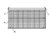
도 1은 상기 종래기술의 엘이디 표시장치의 사시도, 도 2는 도 1의 엘이디 표시장치의 정면도이다.1 is a perspective view of the LED display device of the prior art, Figure 2 is a front view of the LED display device of FIG.
상기 종래기술의 엘이디 표시장치는 도 1 및 도 2와 같이, 전면에 복수의 엘이디픽셀(1)이 길이 방향으로 소정 간격을 두고 설치되며, 후면에 상기 각 엘이디픽셀을 구동하기 위한 구동소자가 설치된 막대 형상의 회로기판으로 이루어진 복수의 엘이디보드(10)와; 각 엘이디보드(10)의 상 측부 또는 하 측부를 각각 지지하는 상측 수평바(21)와 하측 수평바(22), 및 좌측부 또는 우측부를 각각 지지하는 좌측 수직바(23)와 우측 수직바(24)를 구비하여 엘이디보드(10)를 지지하는 고정프레임(20)과; 고정프레임(20)의 일측에 형성되어 구동소자 및 엘이디픽셀(1)과 연결되어 전력을 공급하는 전원공급부(미도시)와; 고정프레임(20)의 일측에 형성되어 복수의 고정프레임을 상하 좌우로 결속시킬 수 있는 상하 결합수단 및 좌우 결합수단;을 포함하여 이루어진다.1 and 2, the LED display device of the related art is provided with a plurality of
상술한 구성을 가지는 종래기술의 엘이디 표시장치는, 엘이디보드(10)를 독립적으로 구성한 후 엘이디보드(10) 사이에 이격 공간(30)을 가지도록 고정프레임(20) 상에 고정함으로써, 전체 무게 및 부피를 최소화시켜 운반 및 설치를 용이하게 하며, 또한, 고정프레임(20) 상에 형성된 이격 공간(30)을 통해 바람, 소리 및 빛이 투과됨으로써 풍압에 대한 저항성을 최소화시키고 방송이나 이벤트 현장 등에서 연출자가 설치공간의 제약을 받지 않고 자유롭게 배치하여 다양한 영상 연출 효과를 확보할 수 있도록 하는 효과를 제공한다.In the conventional LED display device having the above-described configuration, the
그러나 상술한 종래기술의 엘이디 표시장치는 각각의 엘이디보드(10)들과 고정프레임(20)이 별도로 구성되어 있어, 고정프레임(20)을 조립한 후 조립된 고정프레임(20) 상에 엘이디보드(10)들을 부착시키는 작업을 수행하여야 한다.However, in the above-described LED display device of the prior art, each of the
또한, 상기 종래기술의 엘이디 표시장치는 고정프레임(20)에 각각의 엘이디보드(10)을 장착한 후에 각각의 엘이디보드(10)들의 구동을 위한 별도의 전원 및 제어신호 인가를 위한 전원선 및 제어선을 연결 구성하여 하므로 별도의 배선 작업을 수행하여야 한다.In addition, the LED display device according to the related art includes a power line for applying a separate power and control signal for driving each of the
또한, 상기 종래술의 엘이디 표시장치는 각각의 엘이디보드(10)가 별도로 구성되기 때문에 엘이디 표시장치에서 출력되는 영상물의 출력을 제어하기 위하여 엘이디 표시장치의 외부에 별도의 제어장치를 구비하여야 하여야 한다.In addition, the LED display device of the related art should be provided with a separate control device outside the LED display device in order to control the output of the image output from the LED display device because each
따라서 종래기술의 엘이디 표시장치는 설치가 용이하지 않을 뿐만 아니라, 설치에 작업에 많은 시간이 소요되고, 이로 인해 비용 또한 증가하게 되는 문제점, 별도의 제어장치 구비를 위한 설치 면적의 증가 및 추가적인 설치비용이 발생하는 문제점을 가진다.Therefore, the LED display device of the prior art is not only easy to install, but also takes a lot of time for installation, thereby increasing the cost, increase the installation area for the installation of a separate control device and additional installation cost This has a problem that arises.
또한, 상기 종래기술의 엘이디 표시장치는 고정프레임(20)에 장착된 엘이디보드(10)들을 보호하기 위한 별도의 구성을 가지지 않게 되므로, 우천 시 등에 빗물 등이 엘이디보드(10)로 인입되거나, 먼지가 끼이는 것에 의해 합선사고 또는 안전사고가 발생할 수 있는 문제점을 가진다.In addition, since the LED display device of the related art does not have a separate configuration for protecting the
따라서 상술한 종래기술의 문제점을 해결하기 위한 본 발명은, 하중 및 풍압에 대한 저항성을 최소가 되도록 하고, 엘이디 전광판의 설치를 용이하게 하며, 작업시간을 절감시킬 수 있도록 하는 엘이디 전광판용 기판모듈 및 엘이디 전광판을 제공하는 것을 목적으로 한다.Therefore, the present invention for solving the above problems of the prior art, the LED module board module for minimizing the resistance to load and wind pressure, to facilitate the installation of the LED display board, and to reduce the working time and It is an object to provide an LED display board.
본 발명은 또한 전원 및 제어을 위한 배선 작업을 용이하게 수행할 수 있도록 하는 엘이디 전광판용 기판모듈 및 엘이디 전광판을 제공하는 것을 다른 목적으로 한다.Another object of the present invention is to provide an LED display board module and an LED display board which can easily perform a wiring operation for power and control.
본 발명은 또한, 방우, 방습, 방진 특성이 향상된 엘이디 전광판용 기판모듈 및 엘이디 전광판을 제공하는 것을 또 다른 목적으로 한다.Another object of the present invention is to provide an LED display board and an LED display board having improved rainproof, moistureproof, and dustproof characteristics.
상기 목적을 달성하기 위한 본 발명의 엘이디 전광판용 기판 모듈은, 엘이디 픽셀이 행 및 열을 이루도록 배치되며, 상기 엘이디 픽셀의 행 또는 열 사이 영역을 따라 일정 길이를 가지는 통기공들이 형성된 엘이디기판; 상기 통기공에 대응하는 위치별로 지지프레임통기공들이 형성되어 상기 엘이디 기판이 장착되는 지지프레임; 및, 상기 엘이디기판의 표면에 도포층을 형성하도록 상기 엘이디기판이 결합된 상기 지지프레임에 충진되는 충진제;를 포함하여 구성되는 것을 특징으로 한다.The LED display board substrate module of the present invention for achieving the above object is, LED pixels are arranged in rows and columns, the LED substrate is formed with a vent hole having a predetermined length along the area between the rows or columns of the LED pixel; A support frame through which support frame vents are formed for each position corresponding to the vent hole, to which the LED substrate is mounted; And a filler filled in the support frame to which the LED substrate is coupled to form a coating layer on the surface of the LED substrate.
상기 충진제는 상기 엘이디픽셀들이 외부로 노출되도록 충진될 수 있다.The filler may be filled such that the LED pixels are exposed to the outside.
상기 충진제는 또한 상기 엘이디픽셀을 덮는 투명재질일 수도 있다.The filler may also be a transparent material covering the LED pixel.
상기 엘이디기판은, 상기 통기공이 형성되지 않은 상기 엘이디기판의 일 측부의 적어도 하나의 엘이디픽셀 행이 배치되는 영역을 포함하는 제 1 통판부; 상기 엘이디기판의 중앙 영역에서 상기 통기공에 의해 형성되어 상기 엘이디픽셀 열들이 배치되는 엘이디기판띠들을 포함하는 통기부; 상기 통기부의 상기 제 1 통판부의 타측 엘이디기판 단부 영역에서 적어도 하나의 상기 엘이디픽셀 행이 배치되는 영역을 포함하는 제 2 통판부;를 포함하여 일체로 구성될 수 있다.The LED substrate may include: a first plate part including a region in which at least one LED pixel row of one side of the LED substrate on which the vent hole is not formed is disposed; A vent part formed by the vent hole in the central region of the LED substrate and including LED substrate bands on which the LED pixel rows are disposed; And a second plate part including a region in which at least one LED pixel row is disposed in the other LED substrate end region of the first plate part of the vent part.
상기 엘이디기판의 상기 통기공이 형성되지 않은 상부면 및 저면(또는 배면)에는 상기 엘이디기판의 구동을 위한 회로가 배치 형성될 수 있다.Circuits for driving the LED substrate may be disposed on an upper surface and a lower surface (or a rear surface) on which the vent hole of the LED substrate is not formed.
상기 제 1 통판부는, 상기 지지프레임의 고정부가 삽입되는 다수의 고정부삽입구멍; 상기 엘이디기판을 상기 지지프레임에 고정하기 위한 다수의 기판고정공;이 형성될 수 있다.The first plate part may include a plurality of fixing part insertion holes into which the fixing part of the support frame is inserted; A plurality of substrate fixing holes for fixing the LED substrate to the support frame; may be formed.
상기 지지프레임은, 상기 통기공에 대응하는 영역에 관통 형성된 다수의 지지프레임통기공; 상기 지지프레임통기공의 외주연 전체에서 일정 높이로 돌출 형성된 외주리브; 상기 지지프레임통기공의 외주연 전체에서 일정 높이로 돌출 형성된 지지프레임통기공리브;를 포함하며, 상기 외주리브와 상기 지지프레임통기공리브가 상기 엘이디 기판의 제 1 통판부, 제 2 통판부, 엘이디기판띠가 각각 안착되는 제 1 통판부안착부, 제 2 통판부안착부 및 엘이디기판띠안착부를 형성하는 일체형의 판형으로 구성될 수 있다.The support frame, the plurality of support frame through-holes formed in the area corresponding to the vent hole; An outer circumferential rib formed to protrude at a predetermined height from the entire outer circumference of the support frame vent; And a support frame through-hole rib that protrudes to a predetermined height from the entire outer circumference of the support frame through hole. The outer periphery rib and the support frame through-hole rib include a first plate part, a second plate part, and an LED of the LED substrate. The substrate strip may be configured in an integral plate shape to form a first plate portion mounting portion, a second plate portion mounting portion, and an LED substrate strip mounting portion, each of which is seated.
상기 지지프레임은 또한 방열을 위한 방열판을 더 포함하여 구성될 수 있다.The support frame may also be configured to further include a heat sink for heat dissipation.
상기 충진제는 상기 제 1 통판부안착부, 제 2 통판부안착부 및 엘이디기판띠안착부 영역에 충진되는 것을 특징으로 한다.The filler may be filled in the first plate part seating part, the second plate part seating part, and the LED substrate strip seating area.
상기 충진제는 절연, 방진, 방습 기능을 가지는 것을 특징으로 한다.The filler is characterized in that it has an insulation, dustproof, moisture-proof function.
본 발명의 엘이디 전광판은 상기 엘이디 전광판용 기판모듈들이 커넥터에 의해 서로 연결 구성되어 하나의 화면을 출력하는 출력 화면을 형성하도록 설치된다.The LED display board of the present invention is installed so that the board modules for the LED display board are connected to each other by a connector to form an output screen for outputting one screen.
상술한 구성을 가지는 본 발명의 엘이디 전광판용 기판모듈은, 다수의 통기공을 형성하여 부피와 무게를 줄이면서도, 기판모듈의 양 측부에 형성되는 통판부에 의해 엘이디 전광판의 일정 영역을 구성하는 기판모듈을 일체형이 되도록 함으로써 엘이디 전광판을 신속하게 설치할 수 있도록 한다.In the LED module board module of the present invention having the above-described configuration, the board constituting a predetermined region of the LED display board by the plate formed on both sides of the substrate module while reducing the volume and weight by forming a plurality of vent holes By integrating the module, the LED display board can be installed quickly.
또한, 본 발명은 기판모듈의 일측에 기판모듈에 장착되는 엘이디픽셀의 제어를 위한 제어회로를 구성하여, 엘이디 전광판의 저면(또는 배면)에서 상기 엘이디 기판모듈들을 연결하는 전원선 및 제어선 등의 배선을 간결하게 하고 배선 작업을 용이하게 한다.In addition, the present invention constitutes a control circuit for controlling the LED pixel mounted on the substrate module on one side of the substrate module, such as a power line and a control line for connecting the LED substrate modules on the bottom (or back) of the LED display board It simplifies wiring and facilitates wiring.
또한, 본 발명의 엘이디 전광판용 기판모듈은 통기공을 형성하여 풍압을 최소화하고, 일체형으로 구성하여 무게가 감소되면서도 지지력은 더욱 커져, 엘이디 전광판에 부가되는 지지장치들의 구성을 간소화시킴으로써 엘이디 전광판의 제작, 설치 및 유지 보수를 더욱 용이하게 함은 물론 그 비용 또한 현저히 절감시킬 수 있도록 한다.In addition, the LED module board module of the present invention is formed through the ventilation hole to minimize the wind pressure, and by integrally configured to reduce the weight, the support capacity is increased even more, to manufacture the LED display board by simplifying the configuration of the support devices added to the LED display board This makes it easier to install and maintain, as well as significantly reduce its cost.
또한, 본 발명의 엘이디 전광판은 방진 및 방습 기능을 가지는 충진제에 의해 엘이디 기판을 고정함으로써, 엘이디 기판의 고정을 견고히 하고, 빗물, 습기 또는 먼지 등에 의한 고장 발생을 방지하여 전광판의 유지 보수를 용이하게 함은 물론, 내구성을 향상시키고 사용 수명을 증가시킨다.In addition, the LED display board of the present invention by fixing the LED substrate by a filler having a dust and moisture-proof function, to secure the fixing of the LED substrate, to prevent the occurrence of failure due to rain, moisture or dust to facilitate the maintenance of the display board Of course, it also improves durability and increases service life.
이하, 첨부 도면을 참조하여 본 발명을 더욱 상세히 설명한다.Hereinafter, the present invention will be described in more detail with reference to the accompanying drawings.
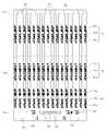
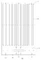
도 3은 본 발명의 일 실시 예에 따르는 엘이디 기판 모듈(이하 "기판모듈(100)"이라 함)의 분해 사시도, 도 4는 도 3의 엘이디기판(101)의 평면(또는 정면)도, 도 5는 도 3의 엘이디 기판의 저면(또는 배면)도, 도 6은 도 3의 지지프레임(110)의 저면(또는 배면)도이다.3 is an exploded perspective view of an LED substrate module (hereinafter referred to as a "
도 3과 같이 상기 기판모듈(100)은 엘이디기판(101)과 지지프레임(110)으로 구성된다.As shown in FIG. 3, the
상기 지지프레임(110)은 엘이디기판(101)이 안착될 수 있는 면적 및 형상을 가지는 통판형으로 형성된다. 상기 지지프레임(110)의 둘레 영역에는 지지프레임(110)의 암착부 면을The
도 3 및 도 4와 같이, 상기 엘이디기판(101)은 제 1 통판부(101a), 통기 공(102)과 엘이디기판띠(102a)로 형성되는 통기부(101b) 및 제 2 통판부(101c)로 영역이 분할되는 일체형의 기판상에 다수의 엘이디픽셀(103)이 행과 열을 이루도록 격자 상으로 배치된 구성을 가진다.As shown in FIGS. 3 and 4, the
상기 제 1 통판부(101a)는 통기공(102)이 형성되지 않은 엘이디기판(101)의 하부의 4개의 엘이디픽셀(103) 행이 배치되는 영역이 된다.The
상기 통기부(101b)는 상기 제 1 통판부(101a)의 상부에서 엘이디기판(101)의 중앙 영역에 형성된 엘이디픽셀(103) 열들이 배치되는 엘이디기판띠(102a)를 형성하도록 엘이디픽셀(103) 열들의 사이 영역이 수직 방향으로 일정 길이로 관통하는 통기공(102)이 형성된 영역이 된다.The
상기 제 2 통판부(101c)는 상기 통기부(101b)의 상부 영역에서 하나의 엘이디픽셀(103) 행이 배치되며 통기공(102)이 형성되지 않은 영역이 된다.The
상기 엘이디기판(101)의 통기공(102)이 형성되지 않은 상부면 및 저면(또는 배면)에는 엘이디기판(101)의 구동을 위한 회로가 프린팅 기법에 의해 형성된다.Circuits for driving the
상기 제 1 통판부(101a)에는 엘이디픽셀(103)들의 구동제어를 위한 구동소자, 버퍼 등을 포함하는 제어회로부(도면에 미 도시)가 배치 구성되고, 엘이디기판(101)을 지지프레임(110)에 고정시키는 경우 지지프레임(110)의 고정부(116, 도 5 참조)가 삽입되는 다수의 고정부삽입구멍(106)이 형성된다. 상기 엘이디기판(101)의 전체 면에는 또한 엘이디기판(101)을 지지프레임(110)에 고정하기 위한 기판고정공(105)들이 형성된다.In the
상기 구성을 가지는 엘이디기판(101)에서 다수의 엘이디픽셀(103)들의 배치 구조를 도4 및 도 5를 참조하여 설명한다.An arrangement structure of the plurality of
도 4와 같이, 상기 엘이디기판(101)의 상부면에서 통기공(102)이 형성되지 않은 영역에는 적색(R), 녹색(G), 청색(B)의 삼색을 표출하는 R, G, B 삼색 엘이디 소자가 일체로 형성된 엘이디픽셀(103)들이 8, 16, 24 등의 행 및 열을 이루도록 배치된다. 이때, 각각의 엘이디픽셀(103)에는 R, G, B 삼색 엘이디 소자의 발광 제어를 위해 R, G, B 삼색 엘이디 소자 각각 형성되는 2개의 단자들이 이루는 6개의 단자가 구비되고, 각각의 6개의 단자 중에서 ▲로 표시된 위치에 엘이디픽셀(103)의 1번 단자가 위치된다.As shown in FIG. 4, R, G, and B expressing three colors of red (R), green (G), and blue (B) in a region where the
그리고 상기 제 1 통판부(101a)에는 엘이디픽셀(103)들의 구동을 제어하는 제어회로(미 도시)가 프린팅 기법에 의해 형성되며, 중앙부에는 커넥터 소켓(109)이 접속되는 커넥터 소켓 접속부(104)가 형성된다.In addition, a control circuit (not shown) for controlling driving of the
다음으로, 상술한 구성을 가지는 엘이디기판(101)의 저면(또는 배면) 구조를 도 5를 참조하여 설명한다.Next, the bottom (or back) structure of the
도 5와 같이 상기 엘이디기판(101)의 저면(또는 배면)에는 상기 통기공(102)의 좌우 측의 엘이디기판띠(102a)의 저면(또는 배면)에 상부면에 배치된 엘이디픽셀(103) 열들 중 일정 개수의 엘이디픽셀(103)들에 대한 R, G, B 삼색 표시 제어를 수행하기 위한 적색 엘이디 드라이버 IC(R 드라이버 IC)(107a), 녹색 엘이디 드라이버 IC(G 드라이버 IC)(107b), 청색 엘이디 드라이버 IC(B 드라이버 IC)(107c)로 구성되는 엘이디 드라이버 IC부(107)들이 일정 간격을 가지는 행 및 열을 형성하도록 배치형성된다. 상기 하나의 엘이디기판(101)의 열에는 24개의 엘이디픽셀(103) 들이 배치되고, R 드라이버 IC(107a)와, G 드라이버 IC(107b)와, B 드라이버 IC(107c)를 포함하는 엘이디 드라이버 IC부(107)가 3행을 이룬다. 따라서 상기 엘이디 드라이버 IC부(107) 중 하나의 엘이디 드라이버 IC열에 구성되는 각각의 R 드라이버 IC(107a)와, G 드라이버 IC(107b)와, B 드라이버 IC(107c)는 24개로 이루어지는 하나의 엘이디픽셀(103) 열에서 각각 8개의 엘이디픽셀(103)에 형성되는 각각의 R, G, B 삼색 엘이디 소자를 제어하게 된다.As shown in FIG. 5, an
상기 제 1 통판부(101a)의 저면(또는 배면)의 영역에는 커넥터 소켓 접속부(104)에 납땜 등에 의해 부착된 커넥터 소켓(109)이 설치되고, 엘이디 전광판의 표출 영상 신호에 대한 데이터의 버퍼링을 위한 다수의 버퍼(108) 및 엘이디기판(101)에 부착되는 전체 엘이디픽셀(103)에 대한 발광 제어를 수행하는 제어회로(미 도시)가 구성된다. 상기 커넥터 소켓(109)에는 인접 기판모듈(100)들 사이에서 전원 및 제어 신호를 송수신할 수 있도록 전원선 및 제어선이 연결된 커넥터(미 도시)가 접속된다.A
상기 도 4 및 도 5의 엘시디픽셀(103)들의 구성은 일 실시 예로서 본원 발명의 엘이디기판(101) 및 엘이디 드라이버 IC부(107)의 개수 및 배치 방식을 제한하는 것은 아니며, 본원발명의 기판모듈(100)은 8, 16, 24 개 등의 다양한 엘이디픽셀 열(또는 행)을 구비하도록 구성되고, 이때 각각의 엘이디 드라이버 IC(107a, 107b, 107c)는 엘이디픽셀 열에 포함되는 엘이디기판(101)의 개수에 따라 적정한 개수의 엘이디픽셀(103)을 제어하도록 선택적으로 구성될 수 있다.The configuration of the
또한, 상술한 도 4 및 도 5의 구성을 가지는 엘이디기판(101)에서 상기 제 1 통판부(101a) 및 제 2 통판부(101c)의 위치는 엘이디기판(101)의 상부 및 하부로 제한되는 것은 아니다. 즉, 상기 제 1 통판부(101a) 및 제 2 통판부(101c)는 상기 통기공(102)의 길이 방향의 양측에 형성되도록 위치되면 족한 것으로서, 통기공(102)의 길이 방향에 따라 엘이디기판(101)의 상하 또는 좌우 측에 형성될 수 있다. 즉, 통기공(102)이 가로 방향으로 형성되는 경우에는 제 1 통판부(101a) 및 제 2 통판부(101c)가 엘이피 기판(101)의 좌측 또는 우측에 각각 형성된다.In addition, the position of the
다음으로, 도 3 및 도 6을 참조하여 상기 지지프레임(110)을 설명한다.Next, the
도 3과 같이 상기 지지프레임(110)은 엘이디기판(101)이 안착될 수 있는 면적 및 형상을 가지는 통판형으로 형성된다. 상기 지지프레임(110)의 통기공(102)에 대응하는 영역 상기 통기공(102)과 동일 면적 및 형상을 가지고 관통되는 지지프레임통기공(102)이 형성된다.As shown in FIG. 3, the
상기 지지프레임(110)의 상부면 중 지지프레임(110)의 전체 둘레에는 일정 높이로 수직으로 돌출된 외주리브(110a)가 형성되며, 상기 지지프레임통기공(102)의 둘레 전체에는 통기공리브(112')가 돌출 형성된다.An outer
상기 구성에 의해 상기 지지프레임(110)의 영역 중 상기 제 1 통판부(101a)가 안착되는 영역은 제 1 통판부안착부(111)가 되고, 상기 지지프레임통기공(112)의 사이 영역은 엘이디기판띠안착부(112b)가 되며, 상기 제 2 통판부(101c)가 안착되는 영역은 제 2 통판부안착부(111c)를 형성한다.The region in which the
그리고 상기 제 1 통판부안착부(111)에는 커넥터 소켓(109)이 관통하여 결합하는 커넥터 소켓 결합구멍(114)과 엘이디기판(101)의 고정부삽입구멍(106)에 삽입 결합하는 고정부(116)가 형성된다. 상기 커넥터 소켓 결합구멍(114)의 전체 둘레에도 수직 방향으로 소켓접속부결합구멍리브(114a)가 돌출 형성된다.The first plate part seating part 111 has a connector
또한 상기 지지프레임(110)은 엘이디기판(101)에서 방출되는 열을 효율적으로 외부로 방출하기 위하여 방열판이 구비될 수 있다.In addition, the
도 7은 본 발명의 또 다른 실시 예에 따르는 상기 방열판(120)이 구비된 지지프레임의 저면(또는 배면)도이다.7 is a bottom (or back) view of the support frame provided with the
도 7과 같이 상기 지지프레임(110)은 배면에는 다수의 리브 형의 방열판(120)이 일 정 간격 및 일정 높이를 가지고 돌출 형성된다. 이때 상기 지지프레임(110)과 상기 방열판(120)들은 모두 열전도성이 우수한 제질로 제작됨으로써 엘이디기판(101)에서 발생하는 열을 지지프레임(110)의 저면(또는 배면)에 형성된 방열판(120)을 통해 배출함으로서 엘이디기판(101) 및 엘이디 전광판()의 과열을 방지한다.As shown in FIG. 7, the
도 8은 상기 엘이디기판(101)과 지지프레임(110)이 결합되어 형성된 기판모듈(100)의 평면(또는 정면)도, 도 9는 도 8의 VIII-VIII선을 따라 절단한 상기 기판모듈(100)의 단면도이다.FIG. 8 is a plan view (or front) of the
상기 엘이디기판(101)의 제 1 통판부(101a), 엘이디기판띠(102a) 및 제 2 통 판부(101c) 각각이 상기 지지프레임(110)의 제 1 통판부안착부(111a), 엘이디기판띠안착부(112b) 및 제 2 통판부안착부(111c)에 결합되고, 상기 커넥터 소켓(109)이 상기 커넥터 소켓 결합구멍(114)에 삽입되도록 상기 엘이디기판(101)이 상기 지지프레임(110)의 상부면에 결합되어 도 8의 기판모듈(100)을 형성한다.Each of the
이때 엘이디기판(101)과 상기 지지프레임(110)은 고정력의 강화, 방진, 방습, 방우, 방풍 또는 절연을 위하여 우레탄, 에폭시 등의 충진제(200)를 매개로 하여 결합될 수 있다.At this time, the
즉, 상기 지지프레임(110)이 제 1 통판부안착부(111a), 엘이디기판띠안착부(112b) 및 제 1 통판부안착부(111a)를 포함하는 안착면에는 우레탄, 에폭시 등의 충진제(200)(도 9 참조)가 충진된다. 이때 충진되는 충진제(200)는 엘이디기판(101)이 결합하는 경우, 엘이디기판(101)이 잠기고, 엘이디픽셀(103)들은 외부로 노출되는 높이를 가지는 양이 충진된다.That is, the
상술한 바와 같이 충진제가 충진된 상기 지지프레임(110)의 상부에 상기 엘이디기판(101)이 상술한 설명과 같은 방식으로 결합한다. 이때 기판고정공(105)에 나사 등을 체결하는 것에 의해 엘이디기판(101)을 지지프레임(110)에 기구적으로 고정시킨다.As described above, the
이 후, 지지프레임(110)을 진동시킨다. 상기 지지프레임(110)의 진동에 의해 상기 엘이디기판(101)이 안착된 제 1 통판부안착부(111a), 엘이디기판띠안착부(112b) 및 제 2 통판부안착부(111c)에서 상기 충진제(200)가 균일한 높이를 가지도록 퍼진다. 이에 의해 상기 엘이디기판(101)은 도 9와 같이 엘이디픽셀(103)을 제외한 모든 영역이 충진제(200)로 도포 된다.Thereafter, the
이후 충진제(200)가 경화되면, 상기 엘이디기판(101)은 충진제(200)에 의해 지지프레임(110)에 견고히 고정된다. 또한, 빗물이나 먼지 등의 이물질이 엘이디기판(101)에 접촉하는 것이 방지되는 방우, 방습, 방진 기능 및 절연 기능을 가지게 된다.After the
이와 달리, 상기 충진제가 에폭시 등의 투명재질인 경우에는 상기 충진제는 상기 엘이디픽셀(103)들도 모두 잠길 수 있는 양으로 지지프레임(110) 상에 충진될 수도 있다. 이 경우에는 엘이디픽셀(103)을 포함하는 엘이디기판(101)이 모두 충진제(200)로 코팅됨으로써 엘이디픽셀(103)에 대한 보호 기능을 구비하게 된다.On the contrary, when the filler is a transparent material such as epoxy, the filler may be filled on the
상술한 바와 같이 결합된 기판모듈(100)은 설치될 엘이디 전광판(도면에 미도시)의 영역을 균등 분할한 영역에 개별적으로 부착되는 설치 단위를 형성한다. 상기 기판모듈(100)은 상기 엘이디 전광판의 각각의 분할된 영역에 설치된 후 고정부삽입구멍(106)을 관통하여 볼트 등의 체결구로 엘이디 전광판을 지지하는 프레임에 체결 고정된 후 커넥터(미 도시)를 통해 연결 구성됨으로써 전체 엘이디 전광판의 화면을 구성한다.The
도 1은 상기 종래기술의 엘이디 표시장치의 사시도,1 is a perspective view of the LED display device of the prior art,
도 2는 도 1의 엘이디 표시장치의 정면도,FIG. 2 is a front view of the LED display device of FIG. 1;
도 3은 본 발명의 일 실시 예에 따르는 엘이디 기판 모듈의 분해 사시도,3 is an exploded perspective view of an LED substrate module according to an embodiment of the present invention;
도 4는 도 3의 엘이디기판(101)의 평면(또는 정면)도,4 is a plan view (or front) of the
도 5는 도 3의 엘이디 기판의 저면(또는 배면)도,5 is a bottom (or back) view of the LED substrate of FIG.
도 6은 도 3의 지지프레임(110)의 저면(또는 배면)도,6 is a bottom (or back) view of the
도 7은 방열판이 구비된 지지프레임(110)의 저면(또는 배면)도이다.7 is a bottom (or back) view of the
도 8은 상기 엘이디기판(101)과 지지프레임(110)이 결합되어 형성된 기판모듈(100)의 평면(또는 정면)도,8 is a plan view (or front) of the
도 9는 도 8의 VIII-VIII선을 따라 절단한 상기 기판모듈(100)의 단면도이다.9 is a cross-sectional view of the
* 도면이 주요 부호에 대한 설명 ** The description of the key symbols in the drawings *
100: 기판모듈101: 엘이디기판100: substrate module 101: LED substrate
101a: 제 1 통판부101b: 통기공부101a:
101c: 제 2 통판부102: 통기공101c: second mailing part 102: ventilator
103: 엘이디픽셀(LED pixel)104: 커넥터 소켓 접속부103: LED pixel 104: connector socket connection
105: 기판고정공106: 고정부삽입구멍105: substrate fixing hole 106: fixing part insertion hole
107: 엘이디 드라이버 IC(LED driver IC)107: LED driver IC
107a: 적색 엘이디 드리이버 IC(R IC)107a: red LED driver IC (R IC)
107b: 녹색 엘이디 드라이버 IC(G IC)107b: Green LED Driver IC (G IC)
107c: 청색 엘이디 드라이버 IC(B IC)107c: blue LED driver IC (B IC)
108: 버퍼109: 커넥터 소켓108: buffer 109: connector socket
110: 지지프레임111a: 제 1 통판부안착부110:
112: 지지프레임통기공112': 통기공리브112: support frame vent 112 ': vent vent
111b: 제 2 통판부안착부114: 커넥터 소켓 결합구멍111b: second plate mounting part 114: connector socket coupling hole
120: 방열판200: 충진제120: heat sink 200: filler
Claims (9)
Translated fromKoreanPriority Applications (1)
| Application Number | Priority Date | Filing Date | Title |
|---|---|---|---|
| KR1020090094023AKR101062303B1 (en) | 2009-10-01 | 2009-10-01 | LED Display Board Substrate Module and LED Display Board |
Applications Claiming Priority (1)
| Application Number | Priority Date | Filing Date | Title |
|---|---|---|---|
| KR1020090094023AKR101062303B1 (en) | 2009-10-01 | 2009-10-01 | LED Display Board Substrate Module and LED Display Board |
Publications (2)
| Publication Number | Publication Date |
|---|---|
| KR20100120258A KR20100120258A (en) | 2010-11-15 |
| KR101062303B1true KR101062303B1 (en) | 2011-09-05 |
Family
ID=43405884
Family Applications (1)
| Application Number | Title | Priority Date | Filing Date |
|---|---|---|---|
| KR1020090094023AActiveKR101062303B1 (en) | 2009-10-01 | 2009-10-01 | LED Display Board Substrate Module and LED Display Board |
Country Status (1)
| Country | Link |
|---|---|
| KR (1) | KR101062303B1 (en) |
Cited By (1)
| Publication number | Priority date | Publication date | Assignee | Title |
|---|---|---|---|---|
| KR20160024294A (en) | 2014-08-25 | 2016-03-04 | 한국전자공업협동조합 | Real time state management system for led electric light panel |
Families Citing this family (7)
| Publication number | Priority date | Publication date | Assignee | Title |
|---|---|---|---|---|
| KR101349081B1 (en)* | 2013-05-15 | 2014-02-11 | 남태순 | Outdoor dustproof led billboards module |
| KR101728492B1 (en)* | 2015-04-24 | 2017-05-02 | 김석배 | Side wall luminescence display device having transparent frame |
| KR101843490B1 (en)* | 2016-04-06 | 2018-03-29 | 강성찬 | Design illuminating device by transparent panel |
| KR102520714B1 (en)* | 2018-07-12 | 2023-04-11 | 삼성전자주식회사 | Display apparatus |
| KR20230122318A (en) | 2022-02-14 | 2023-08-22 | 김재술 | Led light panel |
| KR102455965B1 (en)* | 2022-07-04 | 2022-10-18 | 정연일 | Detachable led signage |
| KR102522816B1 (en)* | 2022-09-14 | 2023-04-19 | 고윤찬 | display panel frame |
Citations (1)
| Publication number | Priority date | Publication date | Assignee | Title |
|---|---|---|---|---|
| KR100654850B1 (en) | 2006-04-24 | 2006-12-08 | (주)베이직테크 | LED display for multi vision |
- 2009
- 2009-10-01KRKR1020090094023Apatent/KR101062303B1/enactiveActive
Patent Citations (1)
| Publication number | Priority date | Publication date | Assignee | Title |
|---|---|---|---|---|
| KR100654850B1 (en) | 2006-04-24 | 2006-12-08 | (주)베이직테크 | LED display for multi vision |
Cited By (1)
| Publication number | Priority date | Publication date | Assignee | Title |
|---|---|---|---|---|
| KR20160024294A (en) | 2014-08-25 | 2016-03-04 | 한국전자공업협동조합 | Real time state management system for led electric light panel |
Also Published As
| Publication number | Publication date |
|---|---|
| KR20100120258A (en) | 2010-11-15 |
Similar Documents
| Publication | Publication Date | Title |
|---|---|---|
| KR101062303B1 (en) | LED Display Board Substrate Module and LED Display Board | |
| US9936561B2 (en) | Flexible LED screen | |
| JP5089857B2 (en) | Large screen LED display system | |
| US6154362A (en) | Display apparatus | |
| KR101156271B1 (en) | Lighting equipment and display device using the same | |
| KR102180594B1 (en) | A LED signboard with curved mounting module and frame | |
| US20110096045A1 (en) | Display apparatus | |
| CN1760936A (en) | Improved display and corresponding support, emissive lighting display modules and packaging for such display modules | |
| WO2010001696A1 (en) | Light source device and illuminating device | |
| US8096682B2 (en) | LED lighting device | |
| CN101694762B (en) | Display screen box body and LED display screen | |
| KR101571097B1 (en) | Large LED sign board and Method of manufacturing the same | |
| JP4961637B2 (en) | Image display unit and image display device | |
| KR102172880B1 (en) | A LED display board with integrated power communication module | |
| US10453383B2 (en) | Display panel having a sealed back cover | |
| KR100786304B1 (en) | Light emitting device, electric light plate having same and manufacturing method thereof | |
| KR102479698B1 (en) | High-resolution LED Signage with Improved Durability and Power Efficiency | |
| JPH0968934A (en) | Display module | |
| JP3640158B2 (en) | Display device | |
| KR20150006193A (en) | Additional installed power supply and controller combining the match box frame, an LED billboard system | |
| KR200464800Y1 (en) | Light emitted diode dispaly unit with radiating structure | |
| CN102194384A (en) | LED (Light Emitting Diode) light emitting board and LED display screen | |
| KR100933780B1 (en) | LED Display Board Substrate Module | |
| JP2011053313A (en) | Led display device | |
| CN212365420U (en) | Display screen unit and double-sided display screen |
Legal Events
| Date | Code | Title | Description |
|---|---|---|---|
| A201 | Request for examination | ||
| PA0109 | Patent application | St.27 status event code:A-0-1-A10-A12-nap-PA0109 | |
| PA0201 | Request for examination | St.27 status event code:A-1-2-D10-D11-exm-PA0201 | |
| R18-X000 | Changes to party contact information recorded | St.27 status event code:A-3-3-R10-R18-oth-X000 | |
| R18-X000 | Changes to party contact information recorded | St.27 status event code:A-3-3-R10-R18-oth-X000 | |
| R18-X000 | Changes to party contact information recorded | St.27 status event code:A-3-3-R10-R18-oth-X000 | |
| G15R | Request for early publication | ||
| R18-X000 | Changes to party contact information recorded | St.27 status event code:A-3-3-R10-R18-oth-X000 | |
| PG1501 | Laying open of application | St.27 status event code:A-1-1-Q10-Q12-nap-PG1501 | |
| E902 | Notification of reason for refusal | ||
| PE0902 | Notice of grounds for rejection | St.27 status event code:A-1-2-D10-D21-exm-PE0902 | |
| P11-X000 | Amendment of application requested | St.27 status event code:A-2-2-P10-P11-nap-X000 | |
| P13-X000 | Application amended | St.27 status event code:A-2-2-P10-P13-nap-X000 | |
| E701 | Decision to grant or registration of patent right | ||
| PE0701 | Decision of registration | St.27 status event code:A-1-2-D10-D22-exm-PE0701 | |
| N231 | Notification of change of applicant | ||
| PN2301 | Change of applicant | St.27 status event code:A-3-3-R10-R13-asn-PN2301 St.27 status event code:A-3-3-R10-R11-asn-PN2301 | |
| GRNT | Written decision to grant | ||
| PR0701 | Registration of establishment | St.27 status event code:A-2-4-F10-F11-exm-PR0701 | |
| PR1002 | Payment of registration fee | St.27 status event code:A-2-2-U10-U11-oth-PR1002 Fee payment year number:1 | |
| PG1601 | Publication of registration | St.27 status event code:A-4-4-Q10-Q13-nap-PG1601 | |
| PN2301 | Change of applicant | St.27 status event code:A-5-5-R10-R11-asn-PN2301 | |
| R18-X000 | Changes to party contact information recorded | St.27 status event code:A-5-5-R10-R18-oth-X000 | |
| PN2301 | Change of applicant | St.27 status event code:A-5-5-R10-R14-asn-PN2301 | |
| FPAY | Annual fee payment | Payment date:20140901 Year of fee payment:4 | |
| PR1001 | Payment of annual fee | St.27 status event code:A-4-4-U10-U11-oth-PR1001 Fee payment year number:4 | |
| P14-X000 | Amendment of ip right document requested | St.27 status event code:A-5-5-P10-P14-nap-X000 | |
| P16-X000 | Ip right document amended | St.27 status event code:A-5-5-P10-P16-nap-X000 | |
| Q16-X000 | A copy of ip right certificate issued | St.27 status event code:A-4-4-Q10-Q16-nap-X000 | |
| P14-X000 | Amendment of ip right document requested | St.27 status event code:A-5-5-P10-P14-nap-X000 | |
| PR1001 | Payment of annual fee | St.27 status event code:A-4-4-U10-U11-oth-PR1001 Fee payment year number:5 | |
| P22-X000 | Classification modified | St.27 status event code:A-4-4-P10-P22-nap-X000 | |
| PR1001 | Payment of annual fee | St.27 status event code:A-4-4-U10-U11-oth-PR1001 Fee payment year number:6 | |
| P14-X000 | Amendment of ip right document requested | St.27 status event code:A-5-5-P10-P14-nap-X000 | |
| R18-X000 | Changes to party contact information recorded | St.27 status event code:A-5-5-R10-R18-oth-X000 | |
| P14-X000 | Amendment of ip right document requested | St.27 status event code:A-5-5-P10-P14-nap-X000 | |
| PR1001 | Payment of annual fee | St.27 status event code:A-4-4-U10-U11-oth-PR1001 Fee payment year number:7 | |
| R18-X000 | Changes to party contact information recorded | St.27 status event code:A-5-5-R10-R18-oth-X000 | |
| P22-X000 | Classification modified | St.27 status event code:A-4-4-P10-P22-nap-X000 | |
| P14-X000 | Amendment of ip right document requested | St.27 status event code:A-5-5-P10-P14-nap-X000 | |
| FPAY | Annual fee payment | Payment date:20180830 Year of fee payment:8 | |
| PR1001 | Payment of annual fee | St.27 status event code:A-4-4-U10-U11-oth-PR1001 Fee payment year number:8 | |
| PR1001 | Payment of annual fee | St.27 status event code:A-4-4-U10-U11-oth-PR1001 Fee payment year number:9 | |
| PR1001 | Payment of annual fee | St.27 status event code:A-4-4-U10-U11-oth-PR1001 Fee payment year number:10 | |
| PN2301 | Change of applicant | St.27 status event code:A-5-5-R10-R13-asn-PN2301 St.27 status event code:A-5-5-R10-R11-asn-PN2301 | |
| P14-X000 | Amendment of ip right document requested | St.27 status event code:A-5-5-P10-P14-nap-X000 | |
| P14-X000 | Amendment of ip right document requested | St.27 status event code:A-5-5-P10-P14-nap-X000 | |
| PR1001 | Payment of annual fee | St.27 status event code:A-4-4-U10-U11-oth-PR1001 Fee payment year number:11 | |
| P14-X000 | Amendment of ip right document requested | St.27 status event code:A-5-5-P10-P14-nap-X000 | |
| PR1001 | Payment of annual fee | St.27 status event code:A-4-4-U10-U11-oth-PR1001 Fee payment year number:12 | |
| P14-X000 | Amendment of ip right document requested | St.27 status event code:A-5-5-P10-P14-nap-X000 | |
| P22-X000 | Classification modified | St.27 status event code:A-4-4-P10-P22-nap-X000 | |
| PR1001 | Payment of annual fee | St.27 status event code:A-4-4-U10-U11-oth-PR1001 Fee payment year number:13 | |
| P14-X000 | Amendment of ip right document requested | St.27 status event code:A-5-5-P10-P14-nap-X000 | |
| PN2301 | Change of applicant | St.27 status event code:A-5-5-R10-R13-asn-PN2301 St.27 status event code:A-5-5-R10-R11-asn-PN2301 | |
| PR1001 | Payment of annual fee | St.27 status event code:A-4-4-U10-U11-oth-PR1001 Fee payment year number:14 | |
| PR1001 | Payment of annual fee | St.27 status event code:A-4-4-U10-U11-oth-PR1001 Fee payment year number:15 |