KR101062029B1 - Gate material planarization to improve gate critical dimensions in semiconductor devices - Google Patents
Gate material planarization to improve gate critical dimensions in semiconductor devicesDownload PDFInfo
- Publication number
- KR101062029B1 KR101062029B1KR1020057008203AKR20057008203AKR101062029B1KR 101062029 B1KR101062029 B1KR 101062029B1KR 1020057008203 AKR1020057008203 AKR 1020057008203AKR 20057008203 AKR20057008203 AKR 20057008203AKR 101062029 B1KR101062029 B1KR 101062029B1
- Authority
- KR
- South Korea
- Prior art keywords
- gate
- gate material
- gate structure
- fin
- layer
- Prior art date
- Legal status (The legal status is an assumption and is not a legal conclusion. Google has not performed a legal analysis and makes no representation as to the accuracy of the status listed.)
- Expired - Lifetime
Links
Images


Classifications
- H—ELECTRICITY
- H01—ELECTRIC ELEMENTS
- H01L—SEMICONDUCTOR DEVICES NOT COVERED BY CLASS H10
- H01L21/00—Processes or apparatus adapted for the manufacture or treatment of semiconductor or solid state devices or of parts thereof
- H01L21/02—Manufacture or treatment of semiconductor devices or of parts thereof
- H01L21/04—Manufacture or treatment of semiconductor devices or of parts thereof the devices having potential barriers, e.g. a PN junction, depletion layer or carrier concentration layer
- H01L21/18—Manufacture or treatment of semiconductor devices or of parts thereof the devices having potential barriers, e.g. a PN junction, depletion layer or carrier concentration layer the devices having semiconductor bodies comprising elements of Group IV of the Periodic Table or AIIIBV compounds with or without impurities, e.g. doping materials
- H—ELECTRICITY
- H10—SEMICONDUCTOR DEVICES; ELECTRIC SOLID-STATE DEVICES NOT OTHERWISE PROVIDED FOR
- H10D—INORGANIC ELECTRIC SEMICONDUCTOR DEVICES
- H10D30/00—Field-effect transistors [FET]
- H10D30/60—Insulated-gate field-effect transistors [IGFET]
- H10D30/67—Thin-film transistors [TFT]
- H10D30/6729—Thin-film transistors [TFT] characterised by the electrodes
- H10D30/673—Thin-film transistors [TFT] characterised by the electrodes characterised by the shapes, relative sizes or dispositions of the gate electrodes
- H—ELECTRICITY
- H10—SEMICONDUCTOR DEVICES; ELECTRIC SOLID-STATE DEVICES NOT OTHERWISE PROVIDED FOR
- H10D—INORGANIC ELECTRIC SEMICONDUCTOR DEVICES
- H10D30/00—Field-effect transistors [FET]
- H10D30/01—Manufacture or treatment
- H10D30/021—Manufacture or treatment of FETs having insulated gates [IGFET]
- H10D30/024—Manufacture or treatment of FETs having insulated gates [IGFET] of fin field-effect transistors [FinFET]
- H—ELECTRICITY
- H10—SEMICONDUCTOR DEVICES; ELECTRIC SOLID-STATE DEVICES NOT OTHERWISE PROVIDED FOR
- H10D—INORGANIC ELECTRIC SEMICONDUCTOR DEVICES
- H10D30/00—Field-effect transistors [FET]
- H10D30/60—Insulated-gate field-effect transistors [IGFET]
- H10D30/62—Fin field-effect transistors [FinFET]
- H10D30/6212—Fin field-effect transistors [FinFET] having fin-shaped semiconductor bodies having non-rectangular cross-sections
Landscapes
- Engineering & Computer Science (AREA)
- Physics & Mathematics (AREA)
- Condensed Matter Physics & Semiconductors (AREA)
- General Physics & Mathematics (AREA)
- Manufacturing & Machinery (AREA)
- Computer Hardware Design (AREA)
- Microelectronics & Electronic Packaging (AREA)
- Power Engineering (AREA)
- Thin Film Transistor (AREA)
- Insulated Gate Type Field-Effect Transistor (AREA)
- Electrodes Of Semiconductors (AREA)
Abstract
Translated fromKoreanDescription
Translated fromKorean본 발명은 반도체 디바이스들 및 반도체 디바이스들을 제조하는 방법들에 관한 것이다. 본 발명은 특히 더블-게이트 디바이스들에 적용가능하다.The present invention relates to semiconductor devices and methods of manufacturing semiconductor devices. The invention is particularly applicable to double-gate devices.
최대 규모 스케일 집적 반도체 디바이스들과 연관된 높은 밀도 및 성능을 위해 점자 증가하는 요구사항들은, 100나노미터(nm) 이하의 게이트 길이, 높은 신뢰도 및 증가된 제조 처리량과 같은 디자인 특성들을 요구한다. 100nm 이하의 디자인 피쳐들의 감소는 종래 방법론의 제한요소들을 해결한다.Braille increasing requirements for the high density and performance associated with the largest scale integrated semiconductor devices require design characteristics such as gate lengths of less than 100 nanometers (nm), high reliability and increased manufacturing throughput. The reduction of design features below 100 nm addresses the limitations of conventional methodology.
예를 들어, 종래 평탄한 금속 산화물 반도체 전계 효과 트랜지스터들(MOSFET들)의 게이트 길이는 100nm 이하로 스케일되고, 소스와 드레인 사이의 과도한 누설과 같은 짧은 채널 효과들과 연관된 문제점들은 점차 극복하기 어려워진다. 게다가, 이동도 감소 및 다수의 공정 문제들은 또한, 점차적으로 더 작은 디바이스 피쳐들을 포함하기 위해 종래 MOSFET들을 스케일하기 어렵게 한다. 따라서, 새로운 디바이스 구조들은 FET 성능을 향상시키기 위해 개발되고, 추가적인 디바이스 스케일링을 허용한다.For example, the gate length of conventional planar metal oxide semiconductor field effect transistors (MOSFETs) scales to 100 nm or less, and problems associated with short channel effects such as excessive leakage between source and drain become increasingly difficult to overcome. In addition, mobility reduction and a number of process problems also make it difficult to scale conventional MOSFETs to include increasingly smaller device features. Thus, new device structures have been developed to improve FET performance and allow for additional device scaling.
더블-게이트 MOSFET들은, 기존의 평탄한 MOSFET들을 계승하기 위한 후보로서 고려되어 온 새로운 구조들을 나타낸다. 몇몇 양상들에서, 더블-게이트 MOSFET들은 종래 벌크 실리콘 MOSFET들보다 더 나은 특성들을 제공한다. 이러한 특성 향상들은, 종래 MOSFET들처럼 오직 채널 한 측에 게이트 전극이 있는 것과 달리, 더블-게이트 MOSFET이 채널 양측에 게이트 전극을 가짐으로 해서 이루어진다. 두 개의 게이트들이 존재할 때, 드레인에 의해 발생된 전계는 채널의 소스 종단으로부터 더 잘 차단(screen)된다. 또한, 두 게이트들은 단일 게이트에 비해 약 2배의 전류로 제어할 수 있고, 그에 따라 스위칭 신호가 더욱 강해진다.Double-gate MOSFETs represent new structures that have been considered as candidates for inheriting existing flat MOSFETs. In some aspects, double-gate MOSFETs provide better characteristics than conventional bulk silicon MOSFETs. These property enhancements are achieved by having a double-gate MOSFET with gate electrodes on both sides of the channel, unlike conventional MOSFETs with only gate electrodes on one side of the channel. When there are two gates, the electric field generated by the drain is better screened from the source end of the channel. In addition, the two gates can be controlled with about twice as much current as a single gate, resulting in a stronger switching signal.
FinFET은 우수한 짧은 채널 동작을 나타내는 최근의 더블-게이트 구조이다. FinFET은 수직 핀(fin)에서 형성된 채널을 포함한다. FinFET 구조는, 종래 평탄한 MOSFET들에 사용되는 것과 유사한 래이아웃 및 공정 기술들을 사용하여 제조될 수 있다.FinFET is a recent double-gate structure that exhibits good short channel operation. FinFETs include channels formed at vertical fins. FinFET structures can be fabricated using layout and processing techniques similar to those used in conventional planar MOSFETs.
본 발명에 따른 실시예들은, 게이트의 임계 치수(CD)를 개선시키는 FinFET 디바이스를 형성하는 방법을 제공한다. 상기 게이트 물질은 게이트 패터닝(patterning) 이전에 평탄화될 수 있다. 게다가, 반사 방지 코팅(antireflective coating)은 평탄화된 게이트 물질 위에 형성될 수 있다.Embodiments in accordance with the present invention provide a method of forming a FinFET device that improves the critical dimension (CD) of a gate. The gate material may be planarized prior to gate patterning. In addition, an antireflective coating can be formed over the planarized gate material.
본 발명의 부가적인 이점들 및 다른 특징들은 후술하는 발명의 상세한 설명에서 부분적으로 언급될 것이고, 하기의 설명을 정독하는 본 기술분야의 통상의 지식을 가진 자에게 일부 명백할 것이며, 본 발명의 실시로부터 인식될 수 있다.Additional advantages and other features of the invention will be set forth in part in the description which follows, and in part will be obvious to those of ordinary skill in the art, reading the following description, and practicing the invention. Can be recognized.
본 발명에 따르면, 상기 및 다른 이점들은 절연체 위에 핀 구조를 형성하는 단계를 포함하는 반도체 디바이스를 제조하는 방법에 의해 부분적으로 이루어질 수 있다. 핀 구조는 측면들 및 상부면을 포함할 수 있다. 상기 방법은 또한, 핀 구조 위에 게이트 물질을 증착하는 단계와, 증착된 게이트 물질을 평탄화하는 단계를 포함한다. 반사 방지 코팅은 상기 평탄화된 게이트 물질 위에 증착될 수 있고, 게이트 구조는 반사 방지 코팅을 사용하는 평탄화된 게이트 물질 외부에 형성될 수 있다.According to the present invention, the above and other advantages can be made in part by a method of manufacturing a semiconductor device that includes forming a fin structure over an insulator. The fin structure can include sides and an upper surface. The method also includes depositing a gate material over the fin structure and planarizing the deposited gate material. An antireflective coating may be deposited over the planarized gate material and the gate structure may be formed outside the planarized gate material using an antireflective coating.
본 발명의 다른 양상에 따르면, 반도체 디바이스를 제조하는 방법은 절연체 위에 핀 구조를 형성하는 단계와 핀 구조 위에 폴리실리콘을 증착하는 단계를 포함한다. 상기 방법은 또한, 평탄한 상부면을 얻기 위하여 폴리실리콘을 연마하는 단계와, 상기 폴리실리콘의 평탄한 상부면 위에 반사 방지 층을 증착하는 단계를 포함한다. 게이트 구조는 반사 방지 층을 사용하여 폴리실리콘으로부터 형성될 수 있다.According to another aspect of the invention, a method of manufacturing a semiconductor device includes forming a fin structure over an insulator and depositing polysilicon over the fin structure. The method also includes polishing polysilicon to obtain a flat top surface, and depositing an antireflective layer over the flat top surface of the polysilicon. The gate structure can be formed from polysilicon using an antireflective layer.
본 발명의 추가적인 양상에 따르면, 반도체 디바이스를 제조하는 방법은 절연체 위에 핀 구조를 형성하는 단계와 핀 구조 위에 폴리실리콘을 증착하는 단계를 포함한다. 상기 방법은 또한, 평탄한 상부면을 얻기 위해 폴리실리콘을 연마하는 단계와, 폴리실리콘의 평탄한 상부면 위에 반사 방지 코팅을 증착하는 단계를 포함한다. 상기 방법은 반사 방지 코팅 위에 포토레지스트 층을 증착하는 단계와, 게이트 구조를 정의하기 위해 포토레지스트 층을 패터닝하는 단계를 더 포함한다. 상기 폴리실리콘은 정의된 게이트 구조 주변으로부터 식각될 수 있다.According to a further aspect of the invention, a method of manufacturing a semiconductor device includes forming a fin structure over an insulator and depositing polysilicon over the fin structure. The method also includes polishing polysilicon to obtain a flat top surface, and depositing an antireflective coating on the flat top surface of the polysilicon. The method further includes depositing a photoresist layer over the antireflective coating and patterning the photoresist layer to define a gate structure. The polysilicon may be etched from around the defined gate structure.
본 발명의 다른 이점들 및 특징들은 후술하는 상세한 설명들로부터 본 기술분야에서 통상의 지식을 가진 자에게 명백하게 될 것이다. 제시되고 설명된 실시예들은, 본 발명을 실시하기 위해 예상되는 최상의 모드의 실례를 제공한다. 본 발명은 본 발명으로부터 벗어남 없이 다양한 명백한 관점에서 수정될 수 있다. 따라서, 도면들은 본질적으로 예시적인 것일 뿐, 제한적인 것으로 간주되지 말아야 할 것이다.Other advantages and features of the present invention will become apparent to those skilled in the art from the following detailed description. The embodiments shown and described provide examples of the best mode contemplated for practicing the invention. The invention can be modified in various obvious respects without departing from the invention. Accordingly, the drawings are illustrative in nature and should not be regarded as limiting.
첨부된 도면들을 참조하며, 동일한 도면부호를 갖는 요소들은 전반에 걸쳐 동일한 요소들을 나타낸다.Referring to the accompanying drawings, elements having the same reference numerals represent the same elements throughout.
도 1은 본 발명의 예시적인 실시예에 따른 핀을 형성하는데 사용될 수 있는 예시적인 층들을 도시한 단면도이다.1 is a cross-sectional view illustrating exemplary layers that may be used to form a fin in accordance with an exemplary embodiment of the present invention.
도 2A는 본 발명의 예시적인 실시예에 따른 핀 구조의 평면도를 개략적으로 도시한다.2A schematically illustrates a top view of a fin structure in accordance with an exemplary embodiment of the present invention.
도 2B는 본 발명의 실시예에 따른 도 2A의 핀 구조의 형태를 도시하는 단면도이다.2B is a cross-sectional view illustrating the form of the fin structure of FIG. 2A according to an embodiment of the present invention.
도 3은 본 발명의 예시적인 실시예에 따른 도 2B의 디바이스 위에 게이트 유전층 및 게이트 물질의 형성하는 것을 도시하는 단면도이다.3 is a cross-sectional view illustrating the formation of a gate dielectric layer and gate material over the device of FIG. 2B in accordance with an exemplary embodiment of the present invention.
도 4는 본 발명의 예시적인 실시예에 따른 도 3의 게이트 물질을 평탄화하는 것을 도시하는 단면도이다.4 is a cross-sectional view illustrating planarization of the gate material of FIG. 3 in accordance with an exemplary embodiment of the present invention.
도 5A는 본 발명의 예시적인 실시예에 따른 FinFET 구조의 평면도를 개략적으로 도시한다.5A schematically illustrates a top view of a FinFET structure according to an exemplary embodiment of the present invention.
도 5B는 본 발명의 예시적인 실시예에 따른 도 5A의 FinFET을 형성하는 것을 도시하는 단면도이다.5B is a cross-sectional view illustrating the formation of the FinFET of FIG. 5A in accordance with an exemplary embodiment of the present invention.
도 6A 및 6B는 본 발명의 또 다른 구현에 따른 핀의 식각 프로파일을 향상시키는 것을 도시하는 단면도이다.6A and 6B are cross-sectional views illustrating improving the etch profile of a fin in accordance with another implementation of the present invention.
도 7A-7C는 본 발명의 또 다른 구현에 따른 소스-드레인 접합 및 게이트의 수직적으로 균일한 도핑을 도시하는 단면도 및 평면도이다.7A-7C are cross-sectional and top views illustrating vertically uniform doping of a source-drain junction and a gate in accordance with another implementation of the present invention.
본example발명을 실시하기Carrying out the invention 위한 최적 Optimal for실시예Example
후술할 본 발명의 상세한 설명은 첨부된 도면들을 참조한다. 서로 다른 도면들에서의 동일한 도면 부호들은 동일한 또는 유사한 요소들로 간주될 수 있다. 또한, 후술할 상세한 설명은 본 발명을 제한하지 않는다. 대신, 본 발명의 범위는 첨부된 청구항들 및 그들의 균등물들에 의해 정의된다.DETAILED DESCRIPTION OF THE PREFERRED EMBODIMENTS The following detailed description of the invention refers to the accompanying drawings. Like reference numerals in different drawings may be considered to be the same or similar elements. In addition, the following detailed description does not limit the invention. Instead, the scope of the invention is defined by the appended claims and their equivalents.
본 발명에 따른 실시예들은, 게이트에서 가장 작은 피쳐 사이즈를 개선시키는 FinFET 디바이스를 형성하는 방법을 제공한다. 가장 작은 피쳐 사이즈를 개선시키기 위하여, 게이트 물질은 게이트 패터닝 이전에 평탄화될 수 있다. 게다가, 반사 방지 코팅은 평탄화된 게이트 물질 위에 형성될 수 있다.Embodiments in accordance with the present invention provide a method of forming a FinFET device that improves the smallest feature size at the gate. To improve the smallest feature size, the gate material can be planarized prior to gate patterning. In addition, an antireflective coating can be formed over the planarized gate material.
도 1은 본 발명의 실시예에 따라 형성된 반도체 디바이스(100)의 단면도를 도시한다. 도 1을 참조하면, 반도체 디바이스(100)는 실리콘 기판(110), 매립 산화물 층(120) 및 매립 산화물 층(120) 위에 형성된 실리콘 층(130)을 포함하는 실리 콘 온 절연체(SOI)를 포함할 수 있다. 매립 산화물 층(120) 및 실리콘 층(130)은 종래 방식으로 기판(110) 위에 형성될 수 있다.1 illustrates a cross-sectional view of a
예시적인 구현으로, 매립 산화물 층(120)은 실리콘 산화물을 포함할 수 있고, 약 1000Å에서 약 3000Å까지의 범위 내에서 두께를 가질 수 있다. 실리콘 층(130)은 약 300Å에서 약 1500Å까지의 범위 내에서 두께를 가지는 단일결정 또는 다중결정 실리콘을 포함할 수 있다. 실리콘 층(130)은 이하에서 더 상세히 설명된 바와 같이, 더블 게이트 트랜지스터 디바이스에 대한 핀 구조를 형성하는데 사용된다.In an exemplary implementation, buried
본 발명에 따른 대안적인 실시예들로서, 기판(110) 및 층(130)은, 게르마늄과 같은 반도체 물질들을 포함할 수 있거나 또는 실리콘-게르마늄과 같은 다른 반도체 물질들의 결합을 포함할 수 있다. 매립 산화물 층(120)은 또한, 다른 유전 물질들을 포함할 수 있다.As alternative embodiments in accordance with the present invention,
실리콘 나이트라이드 층 또는 실리콘 산화물 층(예컨대, SiO2)과 같은 유전층(140)은, 후속적인 식각 공정 동안 보호 캡으로서 동작하도록 실리콘 층(130) 위에 형성될 수 있다. 예시적인 구현으로, 유전층(140)은 약 150Å에서 약 700Å까지의 범위 내의 두께로 증착될 수 있다. 이어서, 포토레지스트 물질은 후속 공정 동안에 포토레지스트 마스크(150)를 형성하기 위하여 증착되고 패터닝될 수 있다. 포토레지스트는 종래 방식으로 증착되고 패터닝될 수 있다.
이어서, 반도체 디바이스(100)가 식각될 수 있고, 포토레지스트 마스크(150)가 제거될 수 있다. 예시적인 실시예로서, 실리콘 층(130)은 종래 방식으로 식각될 수 있으며, 핀을 형성하기 위해 매립 산화물 층(120) 위에서 식각이 종료된다. 핀 형성 후, 소스 및 드레인 영역들은 핀의 각 종단에 인접하게 형성될 수 있다. 예를 들어, 예시적인 실시예로서, 실리콘, 게르마늄, 또는 실리콘과 게르마늄의 혼합물 층은 소스 및 드레인 영역들을 형성하기 위해 종래 방식으로 증착되고, 패터닝되며, 식각될 수 있다.The
도 2A는 그러한 방식으로 형성된 반도체(100)의 핀 구조의 평면도를 개략적으로 도시한다. 본 발명의 예시적인 실시예에 따르면, 소스 영역(220) 및 드레인 영역(230)은 매립 산화물 층(120) 위의 핀(210)에 인접하게 및 핀의 종단에 근접하게 형성될 수 있다.2A schematically illustrates a top view of the fin structure of a
도 2B는 본 발명의 예시적인 실시예에 따른 핀 구조(210)의 형성을 도시하는 도 2A에서의 라인 A-A'에 따른 단면도이다. 상기 설명된 바와 같이, 유전층(140) 및 실리콘 층(130)은 핀(210)을 형성하기 위해 식각될 수 있다. 핀(210)은 실리콘(130) 및 유전체 캡(140)을 포함할 수 있다.2B is a cross sectional view along line A-A 'in FIG. 2A illustrating the formation of a
도 3은 본 발명의 예시적인 실시예에 따른 핀(210) 위에 게이트 유전층 및 게이트 물질의 형성을 도시하는 단면도이다. 유전층은 핀(210) 위에 형성될 수 있다. 예를 들어, 얇은 산화막(310)은 도 3에 도시된 바와 같이 핀(210) 위에 열적으로 성장될 수 있다. 산화막(310)은 약 10Å에서 약 50Å의 두께로 성장될 수 있고, 후속적으로 형성된 게이트 전극에 대한 유전층으로서 동작하도록 핀(210)에서 실리콘(130)의 노출된 측면들 위에 형성될 수 있다. 산화막(310)과 유사하게, 유전체 캡(140)은 핀(210)의 상부면에 전기 절연체를 제공할 수 있다.3 is a cross-sectional view illustrating the formation of a gate dielectric layer and gate material over
게이트 물질 층(320)은 산화막(310)의 형성 후 반도체 디바이스(100) 위에 증착될 수 있다. 게이트 물질 층(320)은 후속적으로 형성된 게이트 전극들을 위한 물질을 포함할 수 있다. 예시적인 구현으로, 게이트 물질 층(320)은 종래 화학 증기 증착(CVD) 또는 다른 잘 알려진 기술을 사용하여 증착된 폴리실리콘을 포함할 수 있다. 대안적으로, 게르마늄, 또는 실리콘과 게르마늄의 혼합물과 같은 다른 반도체 물질들 또는 다양한 금속들이 게이트 물질로서 사용될 수 있다.The
도 4는 본 발명의 예시적인 실시예에 따른 게이트 물질(320)의 평탄화를 도시하는 단면도이다. 게이트 물질(320)을 평탄화하는 것은, 도 3에서 핀(210) 위에 도시된 바와 같은 물질의 임의의 비평탄 돌출부들을 제거할 수 있다. 도 4로 돌아가면, 화학적-기계적 연마(CMP) 또는 다른 종래 기술은, 게이트 물질(320)의 상부면이 실질적으로 평탄화되도록 수행될 수 있다. 하나의 구현으로, 도 4에 도시된 바와 같이, 평탄한 게이트 물질(320)은 절연체 캡(140) 위로 확장될 수 있다. 평탄화 후 게이트 물질(320)의 두께는 약 700Å에서 약 2000Å까지의 범위를 가질 수 있다.4 is a cross-sectional view illustrating planarization of
본 발명의 원리와 일치하는 대안적인 구현으로 (도시되지 않음), 게이트 물질(320)은 절연체 캡(140)의 상부면까지 아래로 평탄화될 수 있다. 게이트 물질(320)의 상부면은 결과적으로 핀(210)에서 절연체 캡(140)의 상부면에 의해 분리화될 수 있다. 그러한 구현으로, 게이트 물질(320)은 두 개의 물리적이고 전기적으로 분리된 게이트들로 패터닝될 수 있다.In an alternative implementation consistent with the principles of the present invention (not shown),
도 5A는 본 발명의 예시적인 실시예에 따르는 반도체 디바이스(100)의 평면도를 개략적으로 도시한다. 도시된 바와 같이, 게이트 구조(510)는 핀(210)의 채널 영역을 가로질러 확장되도록 패터닝될 수 있다. 게이트 구조(510)는 핀(210)의 측면들에 근접한 게이트 부분과, 핀(210)으로부터 일정 간격 떨어져 있는 더 큰 전극 부분을 포함할 수 있다. 게이트 구조(510)의 전극 부분은 바이어싱을 위하여 접근가능한 전기적 컨택을 제공할 수 있거나, 그렇지 않으면 게이트 부분을 제어할 수 있다.5A schematically illustrates a top view of a
도 5B는 본 발명의 예시적인 실시예에 따르는 도 5A의 반도체 디바이스(100)의 형성을 도시하는 단면도이다. 게이트 구조(510)는 리소그래피(lithography)(예컨대, 포토리소그래피)에 의해 게이트 물질 층(320)에서 정의될 수 있다. 바닥 반사 방지 코팅(BARC) 층(520)은 평탄한 게이트 물질 층(320) 위에 증착될 수 있다. 반도체 기술분야에서 통상의 지식을 가진 자에 의해 인식될 수 있는 바와 같이, 포토레지스트는 BARC 층(520) 위에 증착될 수 있고, 게이트 구조(510)의 형태로 패터닝될 수 있다.5B is a cross-sectional view illustrating the formation of the
이어서, 게이트 물질 층(320)은 디바이스(100)의 게이트 물질 층(320)로부터 게이트 구조(510)를 형성하기 위해 선택적으로 식각 수 있다. 평탄한 게이트 물질 층(320)은 BARC 층(520)에 적어도 평탄한 바닥면을 제공할 수 있고, BARC 층(520)의 상부면을 평편하게 하고자 한다. BARC 층(520)은 약 100Å에서 약 500Å까지의 범위 내의 두께를 가질 수 있다. 평탄한 게이트 물질 층(320) 때문에, BARC 층(520) 위의 포토레지스트는 더 정교하게 패터닝될 수 있고, 게이트 구조(510)의 임계 치수(CD)(즉, 그것의 가장 작은 피쳐 사이즈)는 개선될 수 있다. 예를 들면, 약 20nm에서 약 50nm 범위의 게이트 CD들은 CMP로 게이트 물질(320)의 평탄화에 의해 수행될 수 있다. 따라서, 게이트 물질(320)의 평탄한 상부면은, 전형적인 FinFET 게이트를 정의하는 동안 매우 비평탄한 면과 대조적으로, 게이트 구조(510)의 CD를 개선시킬 수 있다.
이어서, 소스/드레인 영역들(220 및 230)이 도핑될 수 있다. 예를 들어, n-타입 또는 p-타입 불순물들이 소스/드레인 영역(220 및 230)에 주입될 수 있다. 특정 주입 도스 및 에너지는 특정한 최종 디바이스 요구사항에 기초하여 선택될 수 있다. 본 기술분야에서 통상의 지식을 가진자는, 회로 요구사항에 기초하여 소스/드레인 주입 공정을 최적화할 수 있을 것이며, 그러한 동작들은 본 발명의 요지를 불필요하게 불명확하게 하지 않도록 이하에서 기술하지 않는다. 게다가, 측벽 스페이서들(도시하지 않음)은 특정한 회로 요구사항들에 기초하여 소스/드레인 접합들의 위치를 제어하기 위하여 소스/드레인 이온 주입 이전에 선택적으로 형성될 수 있다. 이어서, 활성 어닐링은 소스/드레인 영역들(220 및 230)을 활성화시키기 위하여 수행될 수 있다.The source /
따라서, 본 발명에 따르면, 더블-게이트 FinFET에서의 게이트 CD는 BARC 층(520)을 증착하고 게이트를 정의하기 이전에 게이트 물질(320)을 평탄화하여 개선된다. 바람직하게, 결과적인 구조는 우수한 짧은 채널 효과 동작을 나타낸다. 게다가, 본 발명은 향상된 유연성을 제공하며, 종래 공정에 쉽게 통합될 수 있다.Thus, according to the present invention, the gate CD in the double-gate FinFET is improved by planarizing the
다른Other실시예들Examples
몇몇 구현들에서, FinFET의 핀에서 식각 프로파일을 향상시키는 것이 바람직할 것이다. 도 6A는 핀(600)의 전형적인 식각 프로파일을 도시하는 단면도이다. 정규적인 폴리 식각 공정을 사용하여, 핀(600)은 도 6A에 도시된 바와 같이 실리콘 온 절연체 위의 실리콘(SOI) 구조의 매립 산화물 층(605) 위에 형성될 수 있다. 핀(600)은 실리콘(Si) 부분(610), 실리콘 이산화물(SiO2) 층(620), 실리콘 나이트라이드(SiN) 층(630), 및 포토레지스트 마스크 층(640)을 포함할 수 있다. 핀(600)을 형성하기 위해 전형적인 식각 공정을 사용하는 것은, 도 6A에 도시된 "빅 풋팅(big footing)"의 결과를 낳을 수 있고, 여기서 실리콘 부분(610)의 베이스는 핀의 베이스에서 그 폭이 증가된다. 그러한 풋팅은 결과적인 FinFET에서 동일하지 않은 채널 치수를 초래할 수 있다.In some implementations, it would be desirable to improve the etch profile at the fins of the FinFET. 6A is a cross-sectional view illustrating a typical etch profile of the
도 6B는 핀(600)의 향상된 수직 식각 프로파일을 도시하는 단면도이다. T-게이트 또는 노치(notch) 게이트 식각 접근을 사용하여, 도 6B에 도시된 바와 같이 핀(600)은 향상된 프로파일로 실리콘 온 절연체(SOI)의 매립 산화물 층(605) 위에 형성될 수 있다. 먼저, 포토레지스트 층(640)은 적절한 형태로 잘려질 수 있다. SiO2 층(620) 및 SiN 층(630)에 대한 개구는 포토레지스트 층을 제거하여 생성될 수 있다.6B is a cross-sectional view illustrating an improved vertical etch profile of the
나머지 Si 층(610)은 세 가지 단계들, 즉 메인 식각, 소프트 랜딩, 및 오버 식각으로 식각될 수 있다. 메인 식각 단계는 CF4/HBr/Cl2/He-O2기체 혼합물을 사용할 수 있다. 소프트 랜딩 단계는 HBr/He-O2 기체 혼합물을 사용할 수 있다. 오버 식각 단계는 또한, HBr/He-O2 기체 혼합물을 사용할 수 있다. 대안적으로, 본 기술분야에서 통상의 지식을 가진 자에 의해 인정될 수 있는 바와 같이 다른 기체 혼합물이 사용될 수 있다. 소프트 랜딩 및 오버 식각의 기체 비율, 압력, 및 전력을 변화시킴으로써, 핀(600)의 전반적인 식각 프로파일이 수직 프로파일을 형성하기 위해 보상될 수 있다. 더 나은 등방석 식각을 위하여, 필요할 때 소프트 랜딩 및 오버 식각 단계에 Cl2가 추가될 수 있다. 이러한 방식으로, 도 6A에 도시된 핀(600)의 풋팅된 식각 프로파일은 도 6B에 도시된 수직 프로파일로 향상될 수 있다.The remaining
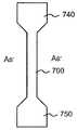
다른 구현들로서, 수직적으로 균일하게 도핑된 접합 및 게이트를 가지는 FinFET이 바람직할 수 있다. 도 7A-7C는 본 발명의 다른 구현에 따른 소스-드레인 접합 및 게이트의 플라즈마 도핑을 도시하는 단면도 및 평면도이다. 게이트(720) 및 스페이서들(730)은 실리콘 층(710) 위에 형성될 수 있다. 실리콘 층(710)은 핀 구조로 형성될 수 있다. 도 7B는 소스 영역(740)과 드레인 영역(750) 사이에 위치된 핀(700)의 평면도를 도시한다.As other implementations, a FinFET with vertically uniformly doped junctions and gates may be desirable. 7A-7C are cross-sectional and top views illustrating plasma doping of a source-drain junction and a gate in accordance with another implementation of the present invention.
게이트(720)의 패터닝 이후에, 소스 영역(740) 및 드레인 영역(750)은 도 7A 및 도 7B에 도시된 바와 같이 플라즈마로 도핑될 수 있다. 하나의 구현으로, 플라즈마는 비소(As)를 포함할 수 있다. 도 7C는 수직적으로 도핑된 소스 및 드레인 영역(740 및 750)을 도시한다. 이러한 방식으로, 소스/드레인 접합은 수직 방향으로 균일하게 도핑될 수 있다.After patterning the
상기 설명들에서, 본 발명의 완전한 이해를 제공하기 위하여 특정 물질들, 구조들, 화학물들, 공정들 등과 같은 수많은 상세한 사항들이 언급된다. 그러나, 본 발명은 여기서 언급된 상세한 사항들에 의존함 없이 실시될 수 있다. 다른 예시들로, 본 발명의 요지를 불필요하게 불명확하게 하지 않도록 잘 알려진 공정 구조들은 상세히 설명되지 않았다.In the above descriptions, numerous details are set forth, such as specific materials, structures, chemicals, processes, etc., to provide a thorough understanding of the present invention. However, the present invention may be practiced without depending on the details mentioned herein. In other instances, well known process structures have not been described in detail so as not to unnecessarily obscure the subject matter of the present invention.
본 발명에 따르면, 반도체 디바이스를 제조하는데 사용되는 유전층 및 전도층들은 종래 증착 기술들에 의해 증착될 수 있다. 예를 들어, 저압 CVD(LPCVD) 및 강화된 CVD(ECVD)를 포함하는 CVD 공정들의 다양한 타입들과 같은 금속화 기술들이 사용될 수 있다.In accordance with the present invention, the dielectric and conductive layers used to fabricate a semiconductor device may be deposited by conventional deposition techniques. For example, metallization techniques, such as various types of CVD processes, including low pressure CVD (LPCVD) and enhanced CVD (ECVD) can be used.
본 발명은 다양한 타입의 반도체 디바이스들 중 어느 하나를 형성하는데 적용할 수 있고, 그에 따라 본 발명의 요지를 불명확하게 하는 것을 피하기 위하여 상세한 사항들은 언급하지 않는다. 본 발명을 실시하는데 있어서, 종래 포토리소그래피 기술 및 식각 기술들이 사용되고, 그에 따라 그러한 기술들의 상세한 설명들이 여기서 상세히 설명되었다.The present invention can be applied to forming any one of various types of semiconductor devices, and thus details are not mentioned in order to avoid obscuring the gist of the present invention. In practicing the present invention, conventional photolithography and etching techniques are used, and thus, the details of such techniques are described in detail herein.
단지 본 발명의 바람직한 실시예들 및 다양한 몇몇 예시들이 본 명세서에 제시되고 설명된다. 본 발명은 다양한 다른 조합들 및 환경들에서 사용될 수 있고, 여기서 표현된 바와 같이 진보적인 개념의 범위 내에서 수정될 수 있다는 것을 인정해야 한다.Only preferred embodiments of the present invention and various various examples are presented and described herein. It should be appreciated that the present invention can be used in a variety of different combinations and environments and can be modified within the scope of the inventive concept as expressed herein.
본 출원의 명세서에 사용된 그 어떠한 요소, 단계, 혹은 지시도 명시적으로 본 발명에 대해 필수적이거나 본질적이라고 설명되지 않은 이상, 본 발명에 대해 필수 또는 본질적이라고 해석되지 않는다. 또한, 본 명세서에서 사용하는 단수는 하나 이상의 아이템들을 나타내는 복수의 의미를 갖는 것으로 의도된다. 오직 하나의 아이템을 나타내는 경우에는 하나 또는 이와 유사한 용어가 사용된다. 본 발명의 범위는 청구항들 및 이들의 균등물에 의해 한정된다. No elements, steps, or instructions used in the specification of this application are to be construed as essential or essential to the invention unless explicitly stated to be essential or essential to the invention. Also, the singular used herein is intended to have the plural meaning of one or more items. When referring to only one item, one or similar terms are used. The scope of the invention is defined by the claims and their equivalents.
Claims (10)
Translated fromKoreanApplications Claiming Priority (3)
| Application Number | Priority Date | Filing Date | Title |
|---|---|---|---|
| US10/290,276US6787439B2 (en) | 2002-11-08 | 2002-11-08 | Method using planarizing gate material to improve gate critical dimension in semiconductor devices |
| US10/290,276 | 2002-11-08 | ||
| PCT/US2003/032655WO2004044973A1 (en) | 2002-11-08 | 2003-10-14 | Planarizing gate material to improve gate critical dimension in semiconductor devices |
Publications (2)
| Publication Number | Publication Date |
|---|---|
| KR20050062655A KR20050062655A (en) | 2005-06-23 |
| KR101062029B1true KR101062029B1 (en) | 2011-09-05 |
Family
ID=32229010
Family Applications (1)
| Application Number | Title | Priority Date | Filing Date |
|---|---|---|---|
| KR1020057008203AExpired - LifetimeKR101062029B1 (en) | 2002-11-08 | 2003-10-14 | Gate material planarization to improve gate critical dimensions in semiconductor devices |
Country Status (8)
| Country | Link |
|---|---|
| US (1) | US6787439B2 (en) |
| EP (1) | EP1559137A1 (en) |
| JP (1) | JP2006505949A (en) |
| KR (1) | KR101062029B1 (en) |
| CN (1) | CN100505182C (en) |
| AU (1) | AU2003282842A1 (en) |
| TW (1) | TWI315548B (en) |
| WO (1) | WO2004044973A1 (en) |
Families Citing this family (43)
| Publication number | Priority date | Publication date | Assignee | Title |
|---|---|---|---|---|
| US7358121B2 (en)* | 2002-08-23 | 2008-04-15 | Intel Corporation | Tri-gate devices and methods of fabrication |
| US7091068B1 (en)* | 2002-12-06 | 2006-08-15 | Advanced Micro Devices, Inc. | Planarizing sacrificial oxide to improve gate critical dimension in semiconductor devices |
| US6872647B1 (en)* | 2003-05-06 | 2005-03-29 | Advanced Micro Devices, Inc. | Method for forming multiple fins in a semiconductor device |
| US6756643B1 (en)* | 2003-06-12 | 2004-06-29 | Advanced Micro Devices, Inc. | Dual silicon layer for chemical mechanical polishing planarization |
| US6909151B2 (en) | 2003-06-27 | 2005-06-21 | Intel Corporation | Nonplanar device with stress incorporation layer and method of fabrication |
| US7456476B2 (en) | 2003-06-27 | 2008-11-25 | Intel Corporation | Nonplanar semiconductor device with partially or fully wrapped around gate electrode and methods of fabrication |
| US7624192B2 (en)* | 2003-12-30 | 2009-11-24 | Microsoft Corporation | Framework for user interaction with multiple network devices |
| US7105390B2 (en)* | 2003-12-30 | 2006-09-12 | Intel Corporation | Nonplanar transistors with metal gate electrodes |
| US7268058B2 (en)* | 2004-01-16 | 2007-09-11 | Intel Corporation | Tri-gate transistors and methods to fabricate same |
| US7115947B2 (en)* | 2004-03-18 | 2006-10-03 | International Business Machines Corporation | Multiple dielectric finfet structure and method |
| US7154118B2 (en) | 2004-03-31 | 2006-12-26 | Intel Corporation | Bulk non-planar transistor having strained enhanced mobility and methods of fabrication |
| CN100461373C (en)* | 2004-05-20 | 2009-02-11 | 中芯国际集成电路制造(上海)有限公司 | Use of chemical and mechanical polishing in joining polycrystalline silicon plug bolt manufacture and arrangement thereof |
| US7579280B2 (en) | 2004-06-01 | 2009-08-25 | Intel Corporation | Method of patterning a film |
| US7042009B2 (en) | 2004-06-30 | 2006-05-09 | Intel Corporation | High mobility tri-gate devices and methods of fabrication |
| US7348284B2 (en) | 2004-08-10 | 2008-03-25 | Intel Corporation | Non-planar pMOS structure with a strained channel region and an integrated strained CMOS flow |
| US7071064B2 (en)* | 2004-09-23 | 2006-07-04 | Intel Corporation | U-gate transistors and methods of fabrication |
| US7332439B2 (en) | 2004-09-29 | 2008-02-19 | Intel Corporation | Metal gate transistors with epitaxial source and drain regions |
| US7422946B2 (en)* | 2004-09-29 | 2008-09-09 | Intel Corporation | Independently accessed double-gate and tri-gate transistors in same process flow |
| US7361958B2 (en) | 2004-09-30 | 2008-04-22 | Intel Corporation | Nonplanar transistors with metal gate electrodes |
| US20060086977A1 (en) | 2004-10-25 | 2006-04-27 | Uday Shah | Nonplanar device with thinned lower body portion and method of fabrication |
| US7193279B2 (en)* | 2005-01-18 | 2007-03-20 | Intel Corporation | Non-planar MOS structure with a strained channel region |
| US7518196B2 (en) | 2005-02-23 | 2009-04-14 | Intel Corporation | Field effect transistor with narrow bandgap source and drain regions and method of fabrication |
| US20060202266A1 (en)* | 2005-03-14 | 2006-09-14 | Marko Radosavljevic | Field effect transistor with metal source/drain regions |
| US7563701B2 (en)* | 2005-03-31 | 2009-07-21 | Intel Corporation | Self-aligned contacts for transistors |
| JP4648096B2 (en)* | 2005-06-03 | 2011-03-09 | 株式会社東芝 | Manufacturing method of semiconductor device |
| US7858481B2 (en) | 2005-06-15 | 2010-12-28 | Intel Corporation | Method for fabricating transistor with thinned channel |
| US7547637B2 (en) | 2005-06-21 | 2009-06-16 | Intel Corporation | Methods for patterning a semiconductor film |
| US7279375B2 (en) | 2005-06-30 | 2007-10-09 | Intel Corporation | Block contact architectures for nanoscale channel transistors |
| US7402875B2 (en)* | 2005-08-17 | 2008-07-22 | Intel Corporation | Lateral undercut of metal gate in SOI device |
| US7479421B2 (en) | 2005-09-28 | 2009-01-20 | Intel Corporation | Process for integrating planar and non-planar CMOS transistors on a bulk substrate and article made thereby |
| US20070090416A1 (en) | 2005-09-28 | 2007-04-26 | Doyle Brian S | CMOS devices with a single work function gate electrode and method of fabrication |
| US7485503B2 (en) | 2005-11-30 | 2009-02-03 | Intel Corporation | Dielectric interface for group III-V semiconductor device |
| US7396711B2 (en) | 2005-12-27 | 2008-07-08 | Intel Corporation | Method of fabricating a multi-cornered film |
| US20070152266A1 (en)* | 2005-12-29 | 2007-07-05 | Intel Corporation | Method and structure for reducing the external resistance of a three-dimensional transistor through use of epitaxial layers |
| US7544594B2 (en)* | 2006-06-28 | 2009-06-09 | Intel Corporation | Method of forming a transistor having gate protection and transistor formed according to the method |
| US8143646B2 (en) | 2006-08-02 | 2012-03-27 | Intel Corporation | Stacking fault and twin blocking barrier for integrating III-V on Si |
| US7435671B2 (en)* | 2006-08-18 | 2008-10-14 | International Business Machines Corporation | Trilayer resist scheme for gate etching applications |
| ES2489615T3 (en)* | 2007-12-11 | 2014-09-02 | Apoteknos Para La Piel, S.L. | Use of a compound derived from p-hydroxyphenyl propionic acid for the treatment of psoriasis |
| US8362566B2 (en) | 2008-06-23 | 2013-01-29 | Intel Corporation | Stress in trigate devices using complimentary gate fill materials |
| JP2010258124A (en)* | 2009-04-23 | 2010-11-11 | Renesas Electronics Corp | Semiconductor device and manufacturing method of semiconductor device |
| CN102386065A (en)* | 2010-09-01 | 2012-03-21 | 无锡华润上华半导体有限公司 | Method of improving photoetching critical dimension uniformity |
| US9041125B2 (en)* | 2013-03-11 | 2015-05-26 | Taiwan Semiconductor Manufacturing Company, Ltd. | Fin shape for fin field-effect transistors and method of forming |
| US11018225B2 (en)* | 2016-06-28 | 2021-05-25 | International Business Machines Corporation | III-V extension by high temperature plasma doping |
Family Cites Families (10)
| Publication number | Priority date | Publication date | Assignee | Title |
|---|---|---|---|---|
| US5315143A (en) | 1992-04-28 | 1994-05-24 | Matsushita Electric Industrial Co., Ltd. | High density integrated semiconductor device |
| US5932911A (en)* | 1996-12-13 | 1999-08-03 | Advanced Micro Devices, Inc. | Bar field effect transistor |
| US6013570A (en) | 1998-07-17 | 2000-01-11 | Advanced Micro Devices, Inc. | LDD transistor using novel gate trim technique |
| JP2000208393A (en)* | 1999-01-12 | 2000-07-28 | Asahi Kasei Microsystems Kk | Fabrication of semiconductor device |
| US6391782B1 (en) | 2000-06-20 | 2002-05-21 | Advanced Micro Devices, Inc. | Process for forming multiple active lines and gate-all-around MOSFET |
| US6396108B1 (en) | 2000-11-13 | 2002-05-28 | Advanced Micro Devices, Inc. | Self-aligned double gate silicon-on-insulator (SOI) device |
| US6475869B1 (en) | 2001-02-26 | 2002-11-05 | Advanced Micro Devices, Inc. | Method of forming a double gate transistor having an epitaxial silicon/germanium channel region |
| JP3543117B2 (en)* | 2001-03-13 | 2004-07-14 | 独立行政法人産業技術総合研究所 | Double gate field effect transistor |
| US6458662B1 (en)* | 2001-04-04 | 2002-10-01 | Advanced Micro Devices, Inc. | Method of fabricating a semiconductor device having an asymmetrical dual-gate silicon-germanium (SiGe) channel MOSFET and a device thereby formed |
| US20020171107A1 (en)* | 2001-05-21 | 2002-11-21 | Baohong Cheng | Method for forming a semiconductor device having elevated source and drain regions |
- 2002
- 2002-11-08USUS10/290,276patent/US6787439B2/ennot_activeExpired - Lifetime
- 2003
- 2003-10-14AUAU2003282842Apatent/AU2003282842A1/ennot_activeAbandoned
- 2003-10-14WOPCT/US2003/032655patent/WO2004044973A1/enactiveApplication Filing
- 2003-10-14KRKR1020057008203Apatent/KR101062029B1/ennot_activeExpired - Lifetime
- 2003-10-14JPJP2004551525Apatent/JP2006505949A/enactivePending
- 2003-10-14EPEP03774839Apatent/EP1559137A1/ennot_activeCeased
- 2003-10-14CNCNB2003801027603Apatent/CN100505182C/ennot_activeExpired - Lifetime
- 2003-11-03TWTW092130613Apatent/TWI315548B/ennot_activeIP Right Cessation
Also Published As
| Publication number | Publication date |
|---|---|
| US6787439B2 (en) | 2004-09-07 |
| KR20050062655A (en) | 2005-06-23 |
| AU2003282842A1 (en) | 2004-06-03 |
| WO2004044973A1 (en) | 2004-05-27 |
| US20040092062A1 (en) | 2004-05-13 |
| EP1559137A1 (en) | 2005-08-03 |
| TW200414326A (en) | 2004-08-01 |
| CN100505182C (en) | 2009-06-24 |
| CN1711630A (en) | 2005-12-21 |
| TWI315548B (en) | 2009-10-01 |
| JP2006505949A (en) | 2006-02-16 |
Similar Documents
| Publication | Publication Date | Title |
|---|---|---|
| KR101062029B1 (en) | Gate material planarization to improve gate critical dimensions in semiconductor devices | |
| KR101029383B1 (en) | Double Gate Semiconductor Devices With Separate Gates | |
| US6645797B1 (en) | Method for forming fins in a FinFET device using sacrificial carbon layer | |
| US6686231B1 (en) | Damascene gate process with sacrificial oxide in semiconductor devices | |
| US6833588B2 (en) | Semiconductor device having a U-shaped gate structure | |
| US6764884B1 (en) | Method for forming a gate in a FinFET device and thinning a fin in a channel region of the FinFET device | |
| US6872647B1 (en) | Method for forming multiple fins in a semiconductor device | |
| US6855607B2 (en) | Multi-step chemical mechanical polishing of a gate area in a FinFET | |
| KR20060123480A (en) | Narrow-body damascene tri-gate finfet hving thinned body | |
| JP2007501524A (en) | Semiconductor devices with variable carrier mobility in semiconductor devices to achieve overall design goals | |
| KR101066270B1 (en) | Damascene triple gate finpet | |
| US6876042B1 (en) | Additional gate control for a double-gate MOSFET | |
| US6911697B1 (en) | Semiconductor device having a thin fin and raised source/drain areas | |
| US6967175B1 (en) | Damascene gate semiconductor processing with local thinning of channel region | |
| US7416925B2 (en) | Doped structure for finfet devices | |
| US6960804B1 (en) | Semiconductor device having a gate structure surrounding a fin | |
| US6995438B1 (en) | Semiconductor device with fully silicided source/drain and damascence metal gate | |
| US7091068B1 (en) | Planarizing sacrificial oxide to improve gate critical dimension in semiconductor devices |
Legal Events
| Date | Code | Title | Description |
|---|---|---|---|
| PA0105 | International application | Patent event date:20050507 Patent event code:PA01051R01D Comment text:International Patent Application | |
| PG1501 | Laying open of application | ||
| A201 | Request for examination | ||
| PA0201 | Request for examination | Patent event code:PA02012R01D Patent event date:20081014 Comment text:Request for Examination of Application | |
| E902 | Notification of reason for refusal | ||
| PE0902 | Notice of grounds for rejection | Comment text:Notification of reason for refusal Patent event date:20100929 Patent event code:PE09021S01D | |
| E701 | Decision to grant or registration of patent right | ||
| PE0701 | Decision of registration | Patent event code:PE07011S01D Comment text:Decision to Grant Registration Patent event date:20110610 | |
| GRNT | Written decision to grant | ||
| PR0701 | Registration of establishment | Comment text:Registration of Establishment Patent event date:20110829 Patent event code:PR07011E01D | |
| PR1002 | Payment of registration fee | Payment date:20110830 End annual number:3 Start annual number:1 | |
| PG1601 | Publication of registration | ||
| FPAY | Annual fee payment | Payment date:20150729 Year of fee payment:5 | |
| PR1001 | Payment of annual fee | Payment date:20150729 Start annual number:5 End annual number:5 | |
| FPAY | Annual fee payment | Payment date:20160727 Year of fee payment:6 | |
| PR1001 | Payment of annual fee | Payment date:20160727 Start annual number:6 End annual number:6 | |
| FPAY | Annual fee payment | Payment date:20170804 Year of fee payment:7 | |
| PR1001 | Payment of annual fee | Payment date:20170804 Start annual number:7 End annual number:7 | |
| FPAY | Annual fee payment | Payment date:20180730 Year of fee payment:8 | |
| PR1001 | Payment of annual fee | Payment date:20180730 Start annual number:8 End annual number:8 | |
| PR1001 | Payment of annual fee | Payment date:20200730 Start annual number:10 End annual number:10 | |
| PR1001 | Payment of annual fee | Payment date:20210728 Start annual number:11 End annual number:11 | |
| PR1001 | Payment of annual fee | Payment date:20220824 Start annual number:12 End annual number:12 | |
| PR1001 | Payment of annual fee | Payment date:20230809 Start annual number:13 End annual number:13 | |
| PC1801 | Expiration of term | Termination date:20240414 Termination category:Expiration of duration |