KR101058106B1 - Display device - Google Patents
Display deviceDownload PDFInfo
- Publication number
- KR101058106B1 KR101058106B1KR1020090072401AKR20090072401AKR101058106B1KR 101058106 B1KR101058106 B1KR 101058106B1KR 1020090072401 AKR1020090072401 AKR 1020090072401AKR 20090072401 AKR20090072401 AKR 20090072401AKR 101058106 B1KR101058106 B1KR 101058106B1
- Authority
- KR
- South Korea
- Prior art keywords
- pattern layer
- layer
- pad
- substrate
- display unit
- Prior art date
- Legal status (The legal status is an assumption and is not a legal conclusion. Google has not performed a legal analysis and makes no representation as to the accuracy of the status listed.)
- Active
Links
Images


Classifications
- G—PHYSICS
- G06—COMPUTING OR CALCULATING; COUNTING
- G06F—ELECTRIC DIGITAL DATA PROCESSING
- G06F3/00—Input arrangements for transferring data to be processed into a form capable of being handled by the computer; Output arrangements for transferring data from processing unit to output unit, e.g. interface arrangements
- G06F3/01—Input arrangements or combined input and output arrangements for interaction between user and computer
- G06F3/03—Arrangements for converting the position or the displacement of a member into a coded form
- G06F3/041—Digitisers, e.g. for touch screens or touch pads, characterised by the transducing means
- G06F3/044—Digitisers, e.g. for touch screens or touch pads, characterised by the transducing means by capacitive means
- G06F3/0446—Digitisers, e.g. for touch screens or touch pads, characterised by the transducing means by capacitive means using a grid-like structure of electrodes in at least two directions, e.g. using row and column electrodes
- G—PHYSICS
- G06—COMPUTING OR CALCULATING; COUNTING
- G06F—ELECTRIC DIGITAL DATA PROCESSING
- G06F3/00—Input arrangements for transferring data to be processed into a form capable of being handled by the computer; Output arrangements for transferring data from processing unit to output unit, e.g. interface arrangements
- G06F3/01—Input arrangements or combined input and output arrangements for interaction between user and computer
- G06F3/03—Arrangements for converting the position or the displacement of a member into a coded form
- G06F3/041—Digitisers, e.g. for touch screens or touch pads, characterised by the transducing means
- G06F3/044—Digitisers, e.g. for touch screens or touch pads, characterised by the transducing means by capacitive means
- G06F3/0443—Digitisers, e.g. for touch screens or touch pads, characterised by the transducing means by capacitive means using a single layer of sensing electrodes
- G—PHYSICS
- G06—COMPUTING OR CALCULATING; COUNTING
- G06F—ELECTRIC DIGITAL DATA PROCESSING
- G06F3/00—Input arrangements for transferring data to be processed into a form capable of being handled by the computer; Output arrangements for transferring data from processing unit to output unit, e.g. interface arrangements
- G06F3/01—Input arrangements or combined input and output arrangements for interaction between user and computer
- G06F3/03—Arrangements for converting the position or the displacement of a member into a coded form
- G06F3/041—Digitisers, e.g. for touch screens or touch pads, characterised by the transducing means
- G06F3/0412—Digitisers structurally integrated in a display
- G—PHYSICS
- G06—COMPUTING OR CALCULATING; COUNTING
- G06F—ELECTRIC DIGITAL DATA PROCESSING
- G06F3/00—Input arrangements for transferring data to be processed into a form capable of being handled by the computer; Output arrangements for transferring data from processing unit to output unit, e.g. interface arrangements
- G06F3/01—Input arrangements or combined input and output arrangements for interaction between user and computer
- G06F3/03—Arrangements for converting the position or the displacement of a member into a coded form
- G06F3/041—Digitisers, e.g. for touch screens or touch pads, characterised by the transducing means
- G06F3/044—Digitisers, e.g. for touch screens or touch pads, characterised by the transducing means by capacitive means
- G06F3/0448—Details of the electrode shape, e.g. for enhancing the detection of touches, for generating specific electric field shapes, for enhancing display quality
- H—ELECTRICITY
- H10—SEMICONDUCTOR DEVICES; ELECTRIC SOLID-STATE DEVICES NOT OTHERWISE PROVIDED FOR
- H10K—ORGANIC ELECTRIC SOLID-STATE DEVICES
- H10K50/00—Organic light-emitting devices
- H10K50/80—Constructional details
- H10K50/86—Arrangements for improving contrast, e.g. preventing reflection of ambient light
- H10K50/865—Arrangements for improving contrast, e.g. preventing reflection of ambient light comprising light absorbing layers, e.g. light-blocking layers
- H—ELECTRICITY
- H10—SEMICONDUCTOR DEVICES; ELECTRIC SOLID-STATE DEVICES NOT OTHERWISE PROVIDED FOR
- H10K—ORGANIC ELECTRIC SOLID-STATE DEVICES
- H10K59/00—Integrated devices, or assemblies of multiple devices, comprising at least one organic light-emitting element covered by group H10K50/00
- H10K59/80—Constructional details
- H10K59/87—Passivation; Containers; Encapsulations
- H10K59/873—Encapsulations
- H—ELECTRICITY
- H10—SEMICONDUCTOR DEVICES; ELECTRIC SOLID-STATE DEVICES NOT OTHERWISE PROVIDED FOR
- H10K—ORGANIC ELECTRIC SOLID-STATE DEVICES
- H10K59/00—Integrated devices, or assemblies of multiple devices, comprising at least one organic light-emitting element covered by group H10K50/00
- H10K59/80—Constructional details
- H10K59/8791—Arrangements for improving contrast, e.g. preventing reflection of ambient light
- H10K59/8792—Arrangements for improving contrast, e.g. preventing reflection of ambient light comprising light absorbing layers, e.g. black layers
- G—PHYSICS
- G06—COMPUTING OR CALCULATING; COUNTING
- G06F—ELECTRIC DIGITAL DATA PROCESSING
- G06F2203/00—Indexing scheme relating to G06F3/00 - G06F3/048
- G06F2203/041—Indexing scheme relating to G06F3/041 - G06F3/045
- G06F2203/04107—Shielding in digitiser, i.e. guard or shielding arrangements, mostly for capacitive touchscreens, e.g. driven shields, driven grounds
- G—PHYSICS
- G06—COMPUTING OR CALCULATING; COUNTING
- G06F—ELECTRIC DIGITAL DATA PROCESSING
- G06F2203/00—Indexing scheme relating to G06F3/00 - G06F3/048
- G06F2203/041—Indexing scheme relating to G06F3/041 - G06F3/045
- G06F2203/04111—Cross over in capacitive digitiser, i.e. details of structures for connecting electrodes of the sensing pattern where the connections cross each other, e.g. bridge structures comprising an insulating layer, or vias through substrate
Landscapes
- Engineering & Computer Science (AREA)
- General Engineering & Computer Science (AREA)
- Theoretical Computer Science (AREA)
- Physics & Mathematics (AREA)
- Human Computer Interaction (AREA)
- General Physics & Mathematics (AREA)
- Optics & Photonics (AREA)
- Quality & Reliability (AREA)
- Electroluminescent Light Sources (AREA)
- Devices For Indicating Variable Information By Combining Individual Elements (AREA)
Abstract
Translated fromKoreanDescription
Translated fromKorean본 발명은 표시 장치에 관한 것으로 더 상세하게는 정전 용량 방식의 터치 패널 기능을 구비한 표시 장치에 관한 것이다. The present invention relates to a display device, and more particularly, to a display device having a capacitive touch panel function.
근래에 표시 장치는 휴대가 가능한 박형의 평판 형태의 표시 장치로 대체되는 추세이다. 또한 이러한 평판 형태의 표시 장치에 터치 패널 기능을 적용하는 기술에 대하여 연구가 진행중이다. 터치 패널 기능을 적용하게 되면 표시 기능만 하던 표시 장치의 패널 표면에 사용자의 손가락이나 펜 등을 접촉하여 입력 장치의 기능도 할 수 있게 된다.In recent years, display devices have been replaced by portable flat panel display devices. In addition, research is being conducted on applying a touch panel function to such a flat panel display device. When the touch panel function is applied, the input device may also function by touching a user's finger or a pen on the surface of the panel of the display device which was only a display function.
그 중 한 방법으로 내장형 정정 용량 방식을 이용한 터치 패널 기능을 적용한 표시 장치의 개발을 위한 연구가 진행중이다. 그러나 표시 장치에서 가시광선을 구현하는 표시부의 구조 및 이를 봉지하는 밀봉부 구조의 정밀성으로 인하여 표시 장치에 정전 용량 방식을 이용한 터치 패널을 장착하는 것은 효과적 생산 측면 및 제품의 특성 측면에서 효율성이 감소하는 문제가 있다.As one of the methods, research is being conducted for the development of a display device applying a touch panel function using a built-in correction capacitance method. However, due to the precision of the structure of the display unit that implements visible light in the display device and the structure of the encapsulation unit that encapsulates the visible light, the mounting of the touch panel using the capacitive method on the display device is effective in terms of production efficiency and product characteristics. there is a problem.
또한 터치 패널 기능을 구현한 표시 장치를 태양광이 입사되는 외부의 환경에서 사용하면 태양광의 반사로 인하여 표시 장치의 콘트라스트가 현저하게 감소하 고, 이로 인하여 표시 장치의 원하는 광학적 특성을 확보하는데 한계가 있다.In addition, when the display device implementing the touch panel function is used in an environment in which sunlight is incident, the contrast of the display device is remarkably reduced due to the reflection of sunlight, and thus there is a limit in securing desired optical characteristics of the display device. have.
본 발명은 광학적 특성을 향상하고 터치 패널 기능을 구비하는 표시 장치를 용이하게 제공할 수 있다.The present invention can easily provide a display device having an optical characteristic and having a touch panel function.
본 발명은 기판, 상기 기판상에 형성되고 복수의 화소들을 구비하는 표시부, 상기 표시부와 대향하도록 상기 표시부를 봉지하도록 배치되는 밀봉 기판, 상기 밀봉 기판 상에 형성된 정전 용량 패턴층 및 상기 기판과 상기 밀봉 기판 사이에 형성되고 상기 화소의 주변에 배치되는 블랙 매트릭스층을 포함하고, 상기 부화소들은 상기 정전 용량 패턴층에 대응하도록 배치된 표시 장치를 개시한다.The present invention provides a substrate, a display portion formed on the substrate and having a plurality of pixels, a sealing substrate disposed to enclose the display portion so as to face the display portion, a capacitance pattern layer formed on the sealing substrate, and the substrate and the sealing. A display device includes a black matrix layer formed between a substrate and disposed around the pixel, and the subpixels are disposed to correspond to the capacitive pattern layer.
본 발명에 있어서 상기 정전 용량 패턴층은 복수 개의 패턴들을 포함하고, 상기 블랙 매트릭스층은 상기 정전 용량 패턴층의 복수 개의 패턴들 사이의 이격된 공간에 배치된 제1 블랙 매트릭스층 및 상기 정전 용량 패턴층 상에 형성된 제2 블랙 매트릭스층을 포함할 수 있다.In the present invention, the capacitive pattern layer includes a plurality of patterns, and the black matrix layer includes a first black matrix layer and the capacitive pattern disposed in spaced spaces between the plurality of patterns of the capacitive pattern layer. It may include a second black matrix layer formed on the layer.
본 발명에 있어서 상기 정전 용량 패턴층은 상기 밀봉 기판의 면 중 상기 표시부를 향하는 면에 형성될 수 있다.In the present invention, the capacitive pattern layer may be formed on a surface of the sealing substrate facing the display unit.
본 발명에 있어서 상기 정전 용량 패턴층은 제1 패턴층 및 상기 제1 패턴층과 전기적으로 절연되는 제2 패턴층을 구비할 수 있다.In the present invention, the capacitance pattern layer may include a first pattern layer and a second pattern layer electrically insulated from the first pattern layer.
본 발명에 있어서 상기 제1 패턴층은 일 방향으로 연장되고, 상기 제2 패턴 층은 상기 제1 패턴층이 연장된 방향과 교차하는 방향으로 연장될 수 있다.In the present invention, the first pattern layer may extend in one direction, and the second pattern layer may extend in a direction crossing the direction in which the first pattern layer extends.
본 발명에 있어서 상기 제1 패턴층은 복수의 제1 패드부 및 인접한 상기 제1 패드부들을 연결하는 제1 연결부를 구비하고 상기 제2 패턴층은 복수의 제2 패드부 및 인접한 상기 제2 패드부들을 연결하는 제2 연결부를 포함할 수 있다.In the present invention, the first pattern layer includes a plurality of first pad portions and a first connection portion connecting the adjacent first pad portions, and the second pattern layer includes a plurality of second pad portions and the adjacent second pads. It may include a second connecting portion for connecting the parts.
본 발명에 있어서 상기 제1 패드부 및 상기 제2 패드부는 마름모 형태일 수 있다.In the present invention, the first pad portion and the second pad portion may have a rhombus shape.
본 발명에 있어서 상기 제1 패드부 및 상기 제2 패드부의 경계선은 상기 화소들의 경계선에 대응하도록 계단 형태를 가질 수 있다.In the present invention, a boundary line between the first pad unit and the second pad unit may have a step shape to correspond to the boundary line of the pixels.
본 발명에 있어서 상기 제1 패턴층 및 상기 제2 패드부들을 덮도록 형성된 제1 절연층을 더 포함하고, 상기 제2 연결부는 상기 제1 절연층에 형성된 콘택홀을 통하여 인접한 상기 제2 패드부를 연결할 수 있다.The method may further include a first insulating layer formed to cover the first pattern layer and the second pad parts, wherein the second connection part is adjacent to the second pad part through a contact hole formed in the first insulating layer. Can connect
본 발명에 있어서 상기 제1 절연층 상에 상기 제2 연결부를 덮도록 형성된 제2 절연층을 더 포함할 수 있다.The present invention may further include a second insulating layer formed to cover the second connection part on the first insulating layer.
본 발명에 있어서 상기 정전 용량 패턴층은 투과형 도전층을 포함할 수 있다.In the present invention, the capacitance pattern layer may include a transmissive conductive layer.
본 발명에 있어서 상기 정전 용량 패턴층은 ITO(indium tin oxide), IZO(indium zinc oxide), IO(indium oxide), GZO(Ga-doped oxide), ZnO(zinc oxide), AZO(Al-doped oxide), FTO(fluorine doped tin oxide), ATO(antimony doped tin oxide) 및 In2O3로 이루어지는 군으로부터 선택된 어느 하나를 포함할 수 있다.In the present invention, the capacitive pattern layer may include indium tin oxide (ITO), indium zinc oxide (IZO), indium oxide (IO), Ga-doped oxide (GZO), zinc oxide (ZnO), and Al-doped oxide (AZO). ), Fluorine doped tin oxide (FTO), antimony doped tin oxide (ATO) and In2 O3 It may include any one selected from the group consisting of.
본 발명에 있어서 상기 화소들은 복수의 부화소들을 구비할 수 있다.In the present invention, the pixels may include a plurality of subpixels.
본 발명에 있어서 상기 표시부는 유기 발광 소자를 구비할 수 있다.In the present invention, the display unit may include an organic light emitting device.
본 발명에 관한 표시 장치는 터치 패널 기능을 용이하게 구현할 수 있다. 또한 본 발명에 관한 표시 장치는 콘트라스트를 향상하여 원하는 광학적 특성을 확보할 수 있다.The display device according to the present invention can easily implement a touch panel function. In addition, the display device according to the present invention can improve contrast to ensure desired optical characteristics.
이하 첨부된 도면들에 도시된 본 발명에 관한 실시예를 참조하여 본 발명의 구성 및 작용을 상세히 설명한다.Hereinafter, with reference to the embodiments of the present invention shown in the accompanying drawings will be described in detail the configuration and operation of the present invention.
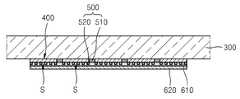
도 1은 본 발명의 일 실시예에 관한 표시 장치를 도시한 개략적인 단면도이고, 도 2는 도 1의 밀봉 기판을 구체적으로 도시한 확대 단면도이다.1 is a schematic cross-sectional view illustrating a display device according to an exemplary embodiment of the present invention, and FIG. 2 is an enlarged cross-sectional view illustrating a sealing substrate of FIG. 1 in detail.
도 1 및 도 2를 참조하면 본 실시예의 표시 장치(1000)는 기판(100), 표시부(200), 밀봉 기판(300), 정전 용량 패턴층(400) 및 블랙 매트릭스층(500)을 포함한다.1 and 2, the
기판(100)은 SiO2를 주성분으로 하는 투명한 유리 재질로 이루어질 수 있다. 기판(100)은 반드시 이에 한정되는 것은 아니며 투명한 플라스틱 재질로 형성할 수도 있다. 플라스틱 재질은 절연성 유기물인 폴리에테르술폰(PES, polyethersulphone), 폴리아크릴레이트(PAR, polyacrylate), 폴리에테르 이미 드(PEI, polyetherimide), 폴리에틸렌 나프탈레이트(PEN, polyethyelenen napthalate), 폴리에틸렌 테레프탈레이드(PET, polyethyeleneterepthalate), 폴리페닐렌 설파이드(polyphenylene sulfide: PPS), 폴리아릴레이트(polyallylate), 폴리이미드(polyimide), 폴리카보네이트(PC), 셀룰로오스 트리 아세테이트(TAC), 셀룰로오스 아세테이트 프로피오네이트(cellulose acetate propionate: CAP)로 이루어진 그룹으로부터 선택되는 유기물일 수 있다.The
화상이 기판(100)방향으로 구현되는 배면 발광형인 경우에 기판(100)은 투명한 재질로 형성해야 한다. 그러나 화상이 기판(100)의 반대 방향으로 구현되는 전면 발광형인 경우에 기판(100)은 반드시 투명한 재질로 형성할 필요는 없다. 이 경우 금속으로 기판(100)을 형성할 수 있다. 금속으로 기판(100)을 형성할 경우 기판(100)은 철, 크롬, 망간, 니켈, 티타늄, 몰리브덴, 스테인레스 스틸(SUS), Invar 합금, Inconel 합금 및 Kovar 합금으로 이루어진 군으로부터 선택된 하나 이상을 포함할 수 있으나, 이에 한정되는 것은 아니다. 기판(100)은 금속 포일로 형성할 수도 있다.When the image is a bottom emission type implemented in the direction of the
기판(100)상에 표시부(200)가 형성된다. 표시부(200)는 가시 광선을 구현할 수 있도록 형성되는데 액정 소자, 전계 발광 소자 또는 유기 발광 소자 등 다양한 종류의 소자를 구비할 수 있다. 표시부(200)는 복수의 화소들을 구비하는데 구체적인 표시부(200)에 대한 구성은 후술하기로 한다.The
표시부(200)상에는 밀봉 기판(300)이 배치된다. 밀봉 기판(300)은 기판(100)의 일 면에 대향하도록 배치되는데, 밀봉 기판(300)은 외부의 수분이나 산소 등으 로부터 표시부(200)를 보호할 수 있고 투명한 재질로 형성된다. 이를 위해 밀봉 기판(300)은 글라스, 플라스틱 또는 유기물과 무기물의 복수의 중첩된 구조를 이용하여 형성할 수 있다. 또한 밀봉 기판(300)은 표시 장치(1000)가 터치 패널 기능을 하도록 사용자의 터치가 이루어지는 부재이다.The
기판(100)과 밀봉 기판(300)은 실런트(150)에 의하여 접합된다. 실런트(150)를 형성하기 위하여 글라스 프릿을 사용할 수 있다. 그 외에 실런트(150)의 재료로는 유기물, 무기물, 유기물과 무기물의 혼합물 등이 사용될 수 있다.The
밀봉 기판(300)의 양 면 중 표시부(200)를 향하는 면에는 정전 용량 패턴층(400), 블랙 매트릭스층(500), 제1 절연층(610) 및 제2 절연층(620)이 차례로 형성되어 있다.The
정전 용량 패턴층(400)은 복수의 패턴을 구비하는데 도전성을 갖는 물질로 형성하고 표시부(200)에서 발생한 가시 광선의 투과를 위하여 투명도가 높은 물질로 형성한다. 정전 용량 패턴층(400)의 구체적인 구성은 후술하기로 한다.The
블랙 매트릭스층(500)은 표시부(200)의 부화소의 주변에 대응하도록 밀봉 기판(300)과 표시부(200)사이에 배치된다. 도 2를 참조하면 블랙 매트릭스층(500)은 제1 블랙 매트릭스층(510) 및 제2 블랙 매트릭스층(520)을 포함한다. 제1 블랙 매트릭스층(510)은 밀봉 기판(300)상에 복수의 정전 용량 패턴층(400)들 사이의 공간에 배치된다. 제2 블랙 매트릭스층(520)은 정전 용량 패턴층(400)상부에 형성된다.The
블랙 매트릭스층(500)은 표시부(200)에서 가시 광선을 실제로 발광하는 화소 주변에 배치되어 각 화소에서 발생한 가시 광선의 진행을 방해하지 않고 빛샘을 방 지하고, 외광의 반사를 방지하여 표시 장치(1000)의 콘트라스트를 향상한다. 결과적으로 표시 장치(1000)의 광학적 특성을 향상한다.The
도 2를 참조하면 블랙 매트릭스층(500)의 제2 블랙 매트릭스층(520)의 형성으로 인하여 공간(S)이 형성된다. 이러한 공간(S)은 표시부(200)의 각 화소들이 대응되는 공간이다. 구체적인 내용은 후술한다.Referring to FIG. 2, a space S is formed due to the formation of the second
도 3은 도 1의 표시부를 도시한 단면도이고, 도 4는 도 3을 확대한 단면도이다.3 is a cross-sectional view illustrating the display unit of FIG. 1, and FIG. 4 is an enlarged cross-sectional view of FIG. 3.
전술한대로 본 실시예의 표시 장치(1000)는 다양한 형태의 표시부(200)를 포함할 수 있는데 그 예로서 유기 발광 소자를 구비한 표시부(200)를 포함할 수 있다.As described above, the
한편 유기 발광 소자를 구비하는 표시부(200)는 구체적으로 수동 구동형 (PM type: passive matrix type)유기 발광 소자와 능동 구동형(AM type: active matrix type)유기 발광 소자를 포함할 수 있는데, 도 4는 도 3의 표시부(200)가 능동 구동형 유기 발광 소자를 구비하는 경우를 설명하기 위한 단면도이다. 도 4는 설명의 편의를 위하여 세 개의 부화소를 구비한 한 개의 화소를 도시하고 있다.Meanwhile, the
도 4를 참조하면 기판(100)상에 박막 트랜지스터(220) 및 유기발광 소자(230)가 형성된다.Referring to FIG. 4, the
구체적으로 설명하면 먼저 기판(100)의 상부에 평활한 면을 형성하고, 기판(100)상부로 불순 원소가 침투하는 것을 차단하기 위하여, 기판(100)의 상부에 버퍼층(211)을 형성한다. 버퍼층(211)은 SiO2 및/또는 SiNx 등으로 형성할 수 있다.In detail, first, a smooth surface is formed on the upper portion of the
버퍼층(211)상에는 박막 트랜지스터(220:TFT)가 형성된다. 이 박막 트랜지스터(220)는 각 부화소별로 적어도 하나씩 형성되는 데, 이 중 하나는 유기 발광 소자(230)에 전기적으로 연결되어 구동 회로부 역할을 한다. 박막 트랜지스터(220)는 크게 활성층(221), 게이트 전극(222), 소스 전극(223) 및 드레인 전극(224)을 포함한다.The thin film transistor 220 (TFT) is formed on the
버퍼층(211)상에 소정 패턴의 활성층(221)이 형성된다. 활성층(221)은 아모퍼스 실리콘 또는 폴리 실리콘과 같은 무기 반도체나 유기 반도체로 형성될 수 있고 소스 영역, 드레인 영역 및 채널 영역을 포함한다.An
소스 및 드레인 영역은 아모퍼스 실리콘 또는 폴리 실리콘으로 형성한 활성층(221)에 불순물을 도핑하여 형성할 수 있다. 3족 원소인 붕소(B)등으로 도핑하면 p-type, 5족 원소인 질소(N)등으로 도핑하면 n-type 반도체를 형성할 수 있다.The source and drain regions may be formed by doping impurities into the
활성층(221)의 상부에는 게이트 절연막(213)이 형성되고, 게이트 절연막(213)상부의 소정 영역에는 게이트 전극(222)이 형성된다. 게이트 절연막(213)은 활성층(221)과 게이트 전극(222)을 절연하기 위한 것으로 유기물 또는 SiNx, SiO2같은 무기물로 형성할 수 있다.A
게이트 전극(222)은 Au, Ag, Cu, Ni, Pt, Pd, Al, Mo, 또는 Al:Nd, Mo:W 합금 등과 같은 금속 또는 금속의 합금으로 이루어질 수 있으나 이에 한정되지 않고 인접층과의 밀착성, 적층되는 층의 평탄성, 전기 저항 및 가공성 등을 고려하여 다 양한 재료를 사용할 수 있다. 게이트 전극(222)은 TFT 온/오프 신호를 인가하는 게이트 라인(미도시)과 연결되어 있다.The
게이트 전극(222)의 상부로는 콘택홀을 구비하는 층간 절연막(215)이 형성된다. 콘택홀을 통해 소스 전극(223) 및 드레인 전극(224)이 각각 활성층(221)의 소스 및 드레인 영역에 접하도록 형성한다. 소스 전극(223) 및 드레인 전극(224)을 이루는 물질은 Au, Pd, Pt, Ni, Rh, Ru, Ir, Os 외에도, Al, Mo, Al:Nd 합금, MoW 합금 등과 같은 2 종 이상의 금속으로 이루어진 합금을 사용할 수 있으며 이에 한정되지는 않는다.An interlayer insulating
이렇게 형성된 박막 트랜지스터(220)는 패시베이션층(217)으로 덮여 보호된다. 패시베이션층(217)은 무기 절연막 및/또는 유기 절연막을 사용할 수 있는데 무기 절연막으로는 SiO2, SiNx, SiON, Al2O3, TiO2, Ta2O5, HfO2, ZrO2, BST, PZT 등이 포함되도록 할 수 있고, 유기 절연막으로는 일반 범용고분자(PMMA, PS), phenol그룹을 갖는 고분자 유도체, 아크릴계 고분자, 이미드계 고분자, 아릴에테르계 고분자, 아마이드계 고분자, 불소계고분자, p-자일렌계 고분자, 비닐알콜계 고분자 및 이들의 블렌드 등이 포함되도록 할 수 있다. 패시베이션층(217)은 무기 절연막과 유기 절연막의 복합 적층체로도 형성될 수 있다.The
드레인 전극(224)을 노출하도록 패시베이션층(217)에 비아홀을 형성하고, 유기 발광 소자(230)를 형성한다. 유기 발광 소자(230)는 제1 전극(231), 중간층(233R, 233G, 233B) 및 제2 전극(235)을 포함한다. 비아홀을 통하여 제1 전 극(231)은 드레인 전극(224)과 전기적으로 연결된다.Via holes are formed in the
그리고 나서 제1 전극(231)을 덮도록 절연물로 화소 정의막(219)(pixel define layer)을 형성한다. 화소 정의막(219)에 소정의 개구를 형성하여 제1 전 극(231)이 노출되도록 한다. 노출된 제1 전극(231)상에 중간층(233R, 233G, 233B)을 형성한다. 그리고, 전체 화소들을 모두 덮도록 제2 전극(235)을 형성한다. 제1 전극(231), 제2 전극(235)은 각각 애노드 전극, 캐소드 전극의 극성을 갖도록 한다. 물론 제1 전극(231), 제2 전극(235)은 각각 캐소드 전극, 애노드 전극의 극성을 가질 수 있다.Then, a pixel define
설명의 편의를 위하여 후술할 중간층(233R, 233G, 233B)의 구성은 제1 전극(231)이 애노드 전극, 제2 전극(235)이 캐소드 전극인 경우로 한정하여 설명하기로 한다.For convenience of description, the configuration of the
중간층(233R, 233G, 233B)은 가시 광선을 발광하도록 유기 발광층을 포함하는데, 유기 발광층은 저분자 유기물 또는 고분자 유기물을 포함할 수 있다.The
중간층(233R, 233G, 233B)의 유기 발광층이 저분자 유기물로 형성되는 경우 유기 발광층을 중심으로 제1 전극(231)의 방향으로 홀 수송층(hole transport layer: HTL) 및 홀 주입층(hole injection layer: HIL) 등이 적층되고, 제2 전극(235) 방향으로 전자 수송층(electron transport layer: ETL) 및 전자 주입층(electron injection layer: EIL) 등이 적층되도록 형성된다. 이외에도 필요에 따라 다양한 층들이 적층될 수 있다. 사용 가능한 유기 재료도 구리 프탈로시아닌(CuPc: copper phthalocyanine), N,N-디(나프탈렌-1-일)-N,N'-디페닐-벤지딘 (N,N'-Di(naphthalene-1-yl)-N,N'-diphenyl-benzidine: NPB) , 트리스-8-하이드록시퀴놀린 알루미늄(tris-8-hydroxyquinoline aluminum)(Alq3) 등을 비롯해 다양하게 적용 가능하다.When the organic light emitting layers of the
한편, 중간층(233R, 233G, 233B)의 유기 발광층이 고분자 유기물로 형성되는 경우에는 유기 발광층을 중심으로 제1 전극(231)의 방향으로 홀 수송층(hole transport layer: HTL)만이 포함될 수 있다. 상기 고분자 홀 수송층은 폴리에틸렌 디히드록시티오펜 (PEDOT: poly-(2,4)-ethylene-dihydroxy thiophene)이나, 폴리아닐린(PANI: polyaniline) 등을 사용하여 잉크젯 프린팅이나 스핀 코팅의 방법에 의해 제1 전극(231) 상부에 형성되며, 고분자 유기 발광층은 PPV, Soluble PPV's, Cyano-PPV, 폴리플루오렌(Polyfluorene) 등을 사용할 수 있으며 잉크젯 프린팅이나 스핀 코팅 또는 레이저를 이용한 열전사방식 등의 통상의 방법으로 컬러 패턴을 형성할 수 있다.When the organic light emitting layers of the
도 4를 참조하면 세 개의 부화소가 도시되어 있고 이 부화소들은 각각 적색, 녹색, 청색의 가시 광선을 발광한다. 이를 위하여 중간층(233R)은 적색의 가시 광선을 발광하는 유기 발광층을 구비하고, 중간층(233G)은 녹색의 가시 광선을 발광하는 유기 발광층을 구비하고, 중간층(233B)은 청색의 가시 광선을 발광하는 유기 발광층을 구비한다.Referring to FIG. 4, three subpixels are shown, which emit red, green, and blue visible light, respectively. To this end, the
전술한 밀봉 기판(300), 정전 용량 패턴층(400) 및 블랙 매트릭스층(500)의 구체적인 설명을 하기로 한다.The sealing
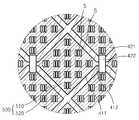
도 5는 도 2의 평면도로서 도 2의 하부에서 본 평면도이다. 도 6a은 도 5를 확대한 도면이고, 도 6b 및 도 6c는 도 6a의 구체적인 변형예이다. 설명의 편의를 위하여 도 5에 제1 절연층(610) 및 제2 절연층(620)은 도시하지 않았다.FIG. 5 is a plan view of FIG. 2, seen from the bottom of FIG. 2. 6A is an enlarged view of FIG. 5, and FIGS. 6B and 6C are modified examples of FIG. 6A. For convenience of description, the first insulating
밀봉 기판(300)상에 형성된 정전 용량 패턴층(400)은 제1 패턴층(410) 및 제2 패턴층(420)을 포함한다.The
제 1 패턴층(410)은 제1 방향(도 5의 X 방향)을 따라 서로 나란하게 형성되어 있는 복수 개의 제1 패드부(411)들, 복수 개의 제1 연결부(412)들, 제1 연장부(413) 및 제1 접속부(414)를 포함한다.The
제2 패턴층(420)은 제1 방향과 실질적으로 수직인 제2 방향(도 5의 Y 방향)을 따라 서로 나란하게 형성되어 있는 복수 개의 제2 패드부(421)들, 복수 개의 제2 연결부(422)들, 제2 연장부(423) 및 제2 접속부(424)를 포함한다.The
이러한 제1 패턴층(410)들과 제2 패턴층(420)들은 서로 교번하여 배치된다. 즉, 밀봉 기판(300) 상에는 복수 개의 제1 패턴층(410)들이 제1 방향(도 5의 X 방향)을 따라 서로 모서리를 맞대며 나란하게 형성되어 있고, 이러한 복수 개의 제1 패턴층(410)들 사이 사이에 복수 개의 제2 패턴층(420)들이 제2 방향(도 5의 Y 방향)을 따라 서로 모서리를 맞대며 나란하게 형성되어 있다고 볼 수 있다.The first pattern layers 410 and the second pattern layers 420 are alternately disposed. That is, the plurality of first pattern layers 410 are formed on the
제1 패턴층(410)과 제2 패턴층(420)의 보다 구체적인 구성은 도 7을 참조하면서 후술하기로 한다.More specific configurations of the
블랙 매트릭스층(500)은 제1 블랙 매트릭스층(510) 및 제2 블랙 매트릭스층(520)을 포함하는데 제1 블랙 매트릭스층(510)은 밀봉 기판(300)상에 배치되고 정전 용량 패턴층(500)들에 구비된 제1 패턴층(410)과 제2 패턴층(420)들 사이의 이격된 공간에 형성된다. 제2 블랙 매트릭스층(520)은 정전 용량 패턴층(400)상에 형성된다.The
블랙 매트릭스층(500)은 표시부(200)의 화소들 주변에 대응하도록 배치되므로 표시부(200)의 화소에 대응하는 영역을 제외한 모든 영역에 형성된다.Since the
도 6a를 참조하면 블랙 매트릭스층(500)이 형성되지 않은 영역(S)은 표시부(200)의 화소에 대응하는 영역이다. 본 발명은 이에 한정되지 않는다. 즉 영역(S)에 각 화소를 이루는 부화소들이 대응할 수도 있다.Referring to FIG. 6A, a region S in which the
도 6b는 도 6a의 변형예를 나타내는데 영역(S)은 각 부화소에 대응되도록 배치된 것을 도시하고 있다. 구체적으로 도 6b의 영역(S)은 즉 도 4에 도시한 적색, 청색, 녹색의 부화소의 중간층(233R, 233G, 233B)에서 가시 광선이 나오는 영역에 대응한다.FIG. 6B illustrates a modification of FIG. 6A, in which the region S is disposed to correspond to each subpixel. Specifically, the region S of FIG. 6B corresponds to a region where visible light is emitted from the
도 6a 및 도 6b를 참조하면 제1 패드부(411) 및 제2 패드부(421)가 마름모꼴로 형성된 것이 도시되어 있다. 그러나 본 발명은 이에 한정되지 않고 다양한 형태를 가질 수 있는데 도 6c는 도 6a의 구체적인 변형예를 도시하고 있다.6A and 6B, the
도 6c를 참조하면 제1 패드부(411) 및 제2 패드부(421)가 계단형태의 외곽선을 갖는 다각형의 형태로 형성된다. 이는 표시부(200)의 화소 또는 부화소의 형태에 대응하는 외곽선을 갖도록 제1 패드부(411) 및 제2 패드부(421)를 형성하기 위함이다.Referring to FIG. 6C, the
도 7은 도 5의 정정 용량 패턴층을 설명하기 위한 도면이다. 정전 용량 패턴층(400)의 구성을 명확히 설명하도록 도 7은 도 5의 블랙 매트릭스층(500), 제2 연 결부(422)를 제거한 상태를 도시하고 있다.FIG. 7 is a diagram for describing the correction capacitance pattern layer of FIG. 5. FIG. 7 illustrates a state in which the
도 7에서 하나의 제1 패턴층(410)을 나타내고 있는 도 7의 수평한 방향으로 도시된 은선 B를 참조하면, 제1 패턴층(410)은 복수 개의 제1 패드부(411)들, 복수 개의 제1 연결부(412)들, 제1 연장부(413) 및 제1 접속부(414)를 포함한다.Referring to the hidden line B shown in the horizontal direction of FIG. 7 showing one
제1 패드부(411)는 제1 방향, 예를 들어 도 7의 X 방향을 따라 복수 개가 일렬로 형성되어 있다. 도 7에는 제1 패드부(411)가 마름모 형태로 도시되어 있으나, 도 6c에 도시한 것과 같이 계단형의 외곽선을 갖도록 제1 패드부(411)가 형성될수도 있다. 제1 연결부(412)는 서로 이웃하고 있는 제1 패드부(411)들 사이에 형성되어, 서로 이웃하고 있는 제1 패드부(411)들 사이를 연결하는 역할을 수행한다.A plurality of
제1 연장부(413)는 제1 패드부(411)들의 일 단부로부터 연장 형성되어 있다. 이 제1 연장부(413)는 일 방향, 예를 들어 도 7의 Y 방향으로 연장되어, 각 제1 연장부(413)들이 모두 밀봉 기판(300)의 일 단부, 즉 도 7에서 보았을 때 상측으로 모이도록 형성될 수 있다. 제1 연장부(413)의 단부에는 제1 접속부(414)가 형성된다.The
한편, 하나의 제2 패턴층(420)을 나타내고 있는 도 7의 은선 C를 참조하면, 제2 패턴층(420)은 각각 복수 개의 제2 패드부(421)들, 제2 연장부(423) 및 제2 접속부(424)를 포함한다. 제2 패드부(421)는 제2 방향, 예를 들어 도 7의 Y 방향을 따라 복수 개가 일렬로 형성되어 있다. 도 7에는 제2 패드부(421)가 마름모 형태로 도시되어 있으나, 도 6c에 도시한 것과 같이 계단형의 외곽선을 갖도록 제2 패드부(421)가 형성될 수도 있다.Meanwhile, referring to the hidden line C of FIG. 7 showing one
각각의 제2 패드부(421)는 제2 연결부에 의하여 연결되는데 도 7에는 제2 연결부를 도시하지 않았다. 제2 연결부에 대한 구체적인 구성은 도 8을 참조하면서 후술하기로 한다. 한편, 제2 연장부(423)는 제2 패드부(421)들의 일 단부로부터 연장 형성되어 있다. 이 제2 연장부(423)는 일 방향, 예를 들어 도 7의 Y 방향으로 연장되어, 각 제2 연장부(423)들이 모두 밀봉 기판(300)의 일 단부, 즉 도 7에서 보았을 때 상측으로 모이도록 형성될 수 있다.Each
제2 연장부(423)의 단부에는 제2 접속부(4214)가 형성된다.A second connection portion 4214 is formed at an end portion of the
도 8은 도 5의 일 부분을 개략적으로 도시한 사시도이다. 설명의 편의를 위하여 제2 절연층은 도시하지 않았다.8 is a perspective view schematically illustrating a part of FIG. 5. For convenience of description, the second insulating layer is not shown.
도 8을 참조하면 제1 패턴층(410) 및 제2 패드부(421)을 덮도록 제1 절연층(610)이 형성되어 있다.Referring to FIG. 8, a first insulating
제1 절연층(610)에 콘택홀(611)이 형성되어 있다. 콘택홀(611)은 제1 절연층(610)의 소정의 위치, 예를 들어 제2 패드부(421)들의 서로 마주보고 있는 모서리 부분에 대응하는 제1 절연층(610)에 형성된다.The
제2 연결부(422)는 제1 절연층(610)의 콘택홀(611)을 채우도록 형성된다. 콘택홀(611)을 통해 제2 패턴층(420)의 각 제2 패드부(421)들은 제2 연결부(422)들과 연결되고, 제2 연결부(422)에 의하여 서로 인접한 제2 패드부(421)들은 전기적으로 연결된다.The
제1 절연층(610)은 제1 패턴층(410)과 제2 패턴층(420)을 절연시키는 역할을 수행하기 위하여 다양한 재료를 이용할 수 있다. 유기물 또는 무기물을 사용할 수 있고 그 예로 실리콘 산화물을 이용할 수 있다.The first insulating
이와 같은 제1 패턴층(410) 및 제2 패턴층(420)의 구성을 통하여, 서로 직교하는 방향으로 형성되어 있는 제1 패드부(411)와 제2 패드부(421)가 서로 교차하지 아니하도록 할 수 있고, 따라서 제1 패드부(411)와 제2 패드부(421) 사이의 쇼트를 방지할 수 있다.Through the configuration of the
도 9는 도 8의 Ⅸ-Ⅸ선을 따라 절취한 단면도이다. 도 9를 참조하면 밀봉 기판(300)상에 제2 패드부(421)와 제1 연결부(412)사이의 이격된 공간에 제1 블랙 매트릭스층(510)이 형성되어 있고, 제2 패드부(421)상에 제2 블랙 매트릭스층(520)이 형성되어 있다. 물론 전술한 대로 제1 블랙 매트릭스층(510) 및 제2 블랙 매트릭스층(520)은 표시부의 화소 또는 부화소들의 주변에 대응하도록 형성된다.9 is a cross-sectional view taken along the line VII-VII of FIG. 8. Referring to FIG. 9, a first
제1 패턴층(410) 및 제2 패턴층(420)은 도전성 패턴으로 형성되고, 표시부(200)에서 발생한 가시 광선을 투과하도록 가시 광선의 투과율이 높은 재료를 이용하여 형성한다. 예를 들어 ITO(indium tin oxide), IZO(indium zinc oxide), IO(indium oxide), GZO(Ga-doped oxide), ZnO(zinc oxide), AZO(Al-doped oxide), FTO(fluorine doped tin oxide), ATO(antimony doped tin oxide) 또는 In2O3등의 투명한 재질로 형성될 수 있다. 그리고, 제1 패턴층(410) 은 포토 리소그래피(photo lithography) 공정을 수행하여 형성될 수 있다. 즉, 증착, 스핀 코팅, 스퍼터링, 잉크젯 등과 같은 방법을 사용하여 형성된 ITO 층을 패터닝하여 제1 패턴층(410)을 형성할 수 있다.The
제1 접속부(414)는 도전성 부재를 통하여 표시부(200)의 데이터 라인들과 연결될 수 있다. 제2 접속부(424)도 제1 접속부(414)와 마찬가지로 도전성 부재를 통하여 표시부(200)의 데이터 라인들과 연결될 수 있다.The
제1 접속부(414) 및 제2 접속부(424)는 낮은 저항값을 갖는 금속을 이용하여 형성할 수 있는데 Mo, Mo합금, Al 및 Ti로 이루어지는 군으로부터 선택된 어느 하나를 포함할 수 있다.The
본 실시예의 유기 발광 표시 장치(1000)는 표면 즉 터치 패널(300)에 사용자의 손과 같은 물체가 접근 또는 접촉할 때, 물체의 접근 또는 접촉으로 인하여 발생하는 정전 용량의 변화를 해석하여 감지한다. 그리고 물체의 접근 또는 접촉이 있는 위치의 좌표 및 압력을 출력하게 된다.The organic light emitting
구체적인 적용의 예를 설명하면, 사용자의 터치 전 표시부(200)의 제2 전극(235)에는 전압이 흐르고 있다. 그러므로 정전 용량 패턴층(400)과 제2 전극(235)은 하나의 커패시터(capacitor)를 형성하고, 정전 용량 패턴층(400)과 제2 전극(235)사이의 정전 용량은 일정하게 유지된다. 이 때 사용자가 밀봉 기판(300)을 터치하면 사용자의 손가락과 정전 용량 패턴층(400)은 또 하나의 커패시터(capacitor)를 형성한다. 이러한 두 개의 커패시터들은 직렬로 연결된 상태로서 사용자의 터치로 인하여 전체적인 정전 용량의 변화가 생긴다. 이와 같은 정전 용량의 변화가 발생한 위치 및 변화의 크기를 감지하여 터치 패널 기능을 구현할 수 있다.In a specific application example, a voltage flows through the
본 발명에 의하면 표시부(200)에서 가시 광선을 구현하는 화소들의 주변에 블랙 매트릭스층(500)을 배치하여 표시 장치(1000)의 콘트라스트를 증가한다. 또한 본 발명의 표시부(200)의 화소들은 모두 정전 용량 패턴층(400)에 대응하도록 형성되어 표시부(200)에서 발생한 가시 광선의 균일한 광특성을 확보할 수 있다. 결과적으로 표시 장치(1000)의 광특성이 향상된다.According to the present invention, the
또한 본 발명에 의하여, 두께의 증가 없이 터치 패널 기능 구현이 가능해지는 효과를 얻을 수 있다. 또한, 밀봉 기판(300)의 내측면에 정전 용량 패턴을 형성하여, 슬림 에칭(slim etching)을 사용하는 것이 가능해졌고, 제1 패턴층 및 제2 패턴층(410, 420)을 용이하게 형성할 수 있다.In addition, according to the present invention, it is possible to obtain the effect that it is possible to implement the touch panel function without increasing the thickness. In addition, by forming a capacitance pattern on the inner surface of the sealing
본 발명은 도면에 도시된 실시예를 참고로 설명되었으나 이는 예시적인 것에 불과하며, 당해 기술 분야에서 통상의 지식을 가진 자라면 이로부터 다양한 변형 및 균등한 다른 실시예가 가능하다는 점을 이해할 것이다. 따라서, 본 발명의 진정한 기술적 보호 범위는 첨부된 특허청구범위의 기술적 사상에 의하여 정해져야 할 것이다.Although the present invention has been described with reference to the embodiments shown in the drawings, these are merely exemplary, and those skilled in the art will understand that various modifications and equivalent other embodiments are possible. Therefore, the true technical protection scope of the present invention will be defined by the technical spirit of the appended claims.
도 1은 본 발명의 일 실시예에 관한 표시 장치를 도시한 개략적인 단면도이다.1 is a schematic cross-sectional view illustrating a display device according to an exemplary embodiment of the present invention.
도 2는 도 1의 밀봉 기판을 구체적으로 도시한 확대 단면도이다.FIG. 2 is an enlarged cross-sectional view specifically illustrating the sealing substrate of FIG. 1.
도 3은 도 1의 표시부를 도시한 단면도이다.3 is a cross-sectional view illustrating the display unit of FIG. 1.
도 4는 도 3을 확대한 단면도이다.4 is an enlarged cross-sectional view of FIG. 3.
도 5는 도 2의 평면도이다.5 is a plan view of FIG. 2.
도 6a은 도 5를 확대한 도면이다.6A is an enlarged view of FIG. 5.
도 6b 및 도 6c는 도 6a의 변형예를 도시한 도면이다.6B and 6C show a modification of FIG. 6A.
도 7은 도 5의 정정 용량 패턴층을 설명하기 위한 도면이다.FIG. 7 is a diagram for describing the correction capacitance pattern layer of FIG. 5.
도 8은 도 5의 일 부분을 개략적으로 도시한 사시도이다.8 is a perspective view schematically illustrating a part of FIG. 5.
도 9는 도 8의 Ⅸ-Ⅸ선을 따라 절취한 단면도이다.9 is a cross-sectional view taken along the line VII-VII of FIG. 8.
<도면의 주요부분에 대한 부호의 간단한 설명>BRIEF DESCRIPTION OF THE DRAWINGS FIG.
1000: 표시 장치 100: 기판1000: display device 100: substrate
150: 실런트200: 표시부150: sealant 200: display unit
300: 밀봉 기판400: 정전 용량 패턴층300: sealing substrate 400: capacitive pattern layer
410: 제1 패턴층 411: 제1 패드부410: first pattern layer 411: first pad portion
412: 제1 연결부 413: 제1 연장부412: first connection portion 413: first extension portion
414: 제1 접속부420: 제2 패턴층414: first connection portion 420: second pattern layer
421: 제2 패드부 422: 제2 연결부421: second pad part 422: second connection part
423: 제2 연장부 424: 제2 접속부423: second extension part 424: second connection part
500: 블랙 매트릭스층 610: 제1 절연층500: black matrix layer 610: first insulating layer
620; 제2 절연층620; Second insulating layer
Claims (14)
Translated fromKoreanPriority Applications (2)
| Application Number | Priority Date | Filing Date | Title |
|---|---|---|---|
| KR1020090072401AKR101058106B1 (en) | 2009-08-06 | 2009-08-06 | Display device |
| US12/790,062US8743078B2 (en) | 2009-08-06 | 2010-05-28 | Display apparatus |
Applications Claiming Priority (1)
| Application Number | Priority Date | Filing Date | Title |
|---|---|---|---|
| KR1020090072401AKR101058106B1 (en) | 2009-08-06 | 2009-08-06 | Display device |
Publications (2)
| Publication Number | Publication Date |
|---|---|
| KR20110014837A KR20110014837A (en) | 2011-02-14 |
| KR101058106B1true KR101058106B1 (en) | 2011-08-24 |
Family
ID=43534465
Family Applications (1)
| Application Number | Title | Priority Date | Filing Date |
|---|---|---|---|
| KR1020090072401AActiveKR101058106B1 (en) | 2009-08-06 | 2009-08-06 | Display device |
Country Status (2)
| Country | Link |
|---|---|
| US (1) | US8743078B2 (en) |
| KR (1) | KR101058106B1 (en) |
Cited By (1)
| Publication number | Priority date | Publication date | Assignee | Title |
|---|---|---|---|---|
| KR20190085505A (en)* | 2019-07-10 | 2019-07-18 | 삼성디스플레이 주식회사 | Organic light emitting display apparatus |
Families Citing this family (48)
| Publication number | Priority date | Publication date | Assignee | Title |
|---|---|---|---|---|
| US8629842B2 (en)* | 2008-07-11 | 2014-01-14 | Samsung Display Co., Ltd. | Organic light emitting display device |
| US8928597B2 (en) | 2008-07-11 | 2015-01-06 | Samsung Display Co., Ltd. | Organic light emitting display device |
| US9342176B2 (en)* | 2008-07-21 | 2016-05-17 | Samsung Display Co., Ltd. | Organic light emitting display device |
| US9753597B2 (en)* | 2009-07-24 | 2017-09-05 | Cypress Semiconductor Corporation | Mutual capacitance sensing array |
| CN102279678A (en)* | 2010-06-12 | 2011-12-14 | 宸鸿科技(厦门)有限公司 | Graphic structure and manufacturing method of touch circuit, touch panel and touch display |
| KR101681123B1 (en)* | 2010-08-20 | 2016-12-02 | 엘지디스플레이 주식회사 | Touch panel and a flat panel display device comprising the same |
| KR101704536B1 (en)* | 2010-10-08 | 2017-02-09 | 삼성전자주식회사 | Touch Panel type of Slim and Portable Device including the same |
| USD661107S1 (en)* | 2010-10-15 | 2012-06-05 | Fujifilm Corporation | Conductive sheet |
| USD661106S1 (en)* | 2010-10-15 | 2012-06-05 | Fujifilm Corporation | Conductive sheet |
| USD661108S1 (en)* | 2010-10-15 | 2012-06-05 | Fujifilm Corporation | Conductive sheet |
| TWD160045S (en)* | 2010-10-19 | 2014-04-21 | 富士軟片股份有限公司 | Portion of conductive sheet pattern |
| USD679100S1 (en)* | 2010-10-19 | 2013-04-02 | Fujifilm Corporation | Conductive sheet with bent portion |
| TWD159640S (en)* | 2010-10-19 | 2014-04-01 | 富士軟片股份有限公司 | Portion of conductive sheet pattern |
| TWI426437B (en)* | 2010-10-28 | 2014-02-11 | Young Lighting Technology Inc | Capacitive touch panel |
| TWD159642S (en)* | 2010-11-24 | 2014-04-01 | 富士軟片股份有限公司 | Portion of conductive sheet pattern |
| JP5675491B2 (en)* | 2011-05-13 | 2015-02-25 | 富士フイルム株式会社 | Conductive sheet and touch panel |
| US9046973B2 (en)* | 2011-06-01 | 2015-06-02 | Scriptel Corporation | Touch screen system |
| US9400576B2 (en) | 2011-07-19 | 2016-07-26 | Apple Inc. | Touch sensor arrangements for organic light-emitting diode displays |
| US20140320761A1 (en)* | 2011-09-02 | 2014-10-30 | Sharp Kabushiki Kaisha | Touch panel and display apparatus |
| WO2013129810A1 (en)* | 2012-02-29 | 2013-09-06 | 미래나노텍 주식회사 | Touch screen sensor, image display device having same, and manufacturing method therefor |
| WO2013145958A1 (en)* | 2012-03-26 | 2013-10-03 | シャープ株式会社 | Touch panel substrate, display panel, and display apparatus |
| TWI588718B (en)* | 2012-03-28 | 2017-06-21 | 友達光電股份有限公司 | Touch panel and method of fabricating the same |
| TWI468820B (en)* | 2012-04-18 | 2015-01-11 | Ind Tech Res Inst | Touch sensor |
| KR101944503B1 (en)* | 2012-06-21 | 2019-04-18 | 삼성디스플레이 주식회사 | Sensor substrate and sensing display panel having the same |
| CN103293749A (en)* | 2012-09-26 | 2013-09-11 | 上海天马微电子有限公司 | Color film substrate of embedded liquid crystal touch screen and embedded liquid crystal touch screen |
| KR102056110B1 (en)* | 2012-10-04 | 2019-12-16 | 삼성전자주식회사 | Touch panel |
| JP2014106974A (en)* | 2012-11-22 | 2014-06-09 | Lg Innotek Co Ltd | Touch window |
| KR101453880B1 (en)* | 2012-11-29 | 2014-10-22 | 삼성디스플레이 주식회사 | Organic light emitting display apparatus and the method for manufacturing the same |
| CN203250289U (en)* | 2012-12-27 | 2013-10-23 | 宸鸿光电科技股份有限公司 | touch panel |
| KR102074418B1 (en)* | 2013-01-29 | 2020-02-07 | 삼성디스플레이 주식회사 | flexible touch screen panel |
| TWI488084B (en)* | 2013-02-08 | 2015-06-11 | Acer Inc | Touch panel |
| JP6131071B2 (en)* | 2013-03-14 | 2017-05-17 | 株式会社ジャパンディスプレイ | Touch panel built-in display device |
| KR102194818B1 (en)* | 2013-08-06 | 2020-12-24 | 삼성디스플레이 주식회사 | Flexible touch display panel |
| JP2015148953A (en)* | 2014-02-06 | 2015-08-20 | 株式会社ジャパンディスプレイ | Capacitive coupling type touch panel |
| KR102215853B1 (en)* | 2014-03-10 | 2021-02-17 | 삼성디스플레이 주식회사 | Display substrate and method of manufacturing the same |
| CN105334994A (en)* | 2014-08-06 | 2016-02-17 | 上海和辉光电有限公司 | OLED touch display panel |
| KR102000716B1 (en)* | 2014-08-26 | 2019-07-17 | 삼성디스플레이 주식회사 | Organic light emitting display apparatus and the method for manufacturing the same |
| KR102276997B1 (en)* | 2014-10-13 | 2021-07-14 | 삼성디스플레이 주식회사 | Display device with touch sensor |
| KR102299875B1 (en) | 2014-11-07 | 2021-09-07 | 엘지디스플레이 주식회사 | Touch panel, method of manufacturing the same and touch panel integrated organic light emitting display device |
| KR102269919B1 (en)* | 2014-12-12 | 2021-06-28 | 삼성디스플레이 주식회사 | Display device comprising touch sensor |
| KR102352741B1 (en)* | 2015-01-14 | 2022-01-18 | 삼성디스플레이 주식회사 | Display device |
| US10173393B2 (en)* | 2015-03-24 | 2019-01-08 | Kaneka Corporation | Transparent electrode-equipped substrate and method for producing transparent electrode-equipped substrate |
| JP6842362B2 (en)* | 2017-05-12 | 2021-03-17 | 株式会社ジャパンディスプレイ | Display device |
| JP2019036005A (en)* | 2017-08-10 | 2019-03-07 | 株式会社ジャパンディスプレイ | Display apparatus and method of manufacturing display apparatus |
| KR102414056B1 (en) | 2018-09-19 | 2022-06-28 | 삼성디스플레이 주식회사 | Touch sensing unit and display apparatus including the same |
| KR102582641B1 (en) | 2018-11-30 | 2023-09-26 | 삼성디스플레이 주식회사 | Electronic panel and electronic apparatus including the same |
| KR102769392B1 (en) | 2019-04-15 | 2025-02-20 | 삼성디스플레이 주식회사 | Electronic apparatus |
| KR20210070459A (en) | 2019-12-04 | 2021-06-15 | 삼성디스플레이 주식회사 | Electronic apparatus |
Family Cites Families (65)
| Publication number | Priority date | Publication date | Assignee | Title |
|---|---|---|---|---|
| JPH03134925A (en) | 1989-10-20 | 1991-06-07 | Toshiba Corp | gas insulated disconnect switch |
| JP2653014B2 (en)* | 1993-07-26 | 1997-09-10 | 日本電気株式会社 | Active matrix liquid crystal display device |
| US7663607B2 (en)* | 2004-05-06 | 2010-02-16 | Apple Inc. | Multipoint touchscreen |
| US6512512B1 (en)* | 1999-07-31 | 2003-01-28 | Litton Systems, Inc. | Touch panel with improved optical performance |
| US6664950B1 (en)* | 1999-11-17 | 2003-12-16 | L-3 Communications | Resistive touch panel using removable, tensioned top layer |
| JP3384397B2 (en)* | 2000-05-25 | 2003-03-10 | セイコーエプソン株式会社 | Liquid crystal device, manufacturing method thereof, and electronic equipment |
| US6980184B1 (en)* | 2000-09-27 | 2005-12-27 | Alien Technology Corporation | Display devices and integrated circuits |
| JP4092914B2 (en)* | 2001-01-26 | 2008-05-28 | セイコーエプソン株式会社 | MASK MANUFACTURING METHOD, ORGANIC ELECTROLUMINESCENT DEVICE MANUFACTURING METHOD |
| KR20030028973A (en) | 2001-10-05 | 2003-04-11 | 비오이 하이디스 테크놀로지 주식회사 | Touch type lcd device |
| JP4507480B2 (en) | 2001-12-27 | 2010-07-21 | ソニー株式会社 | Display device |
| CN1643693A (en) | 2002-03-20 | 2005-07-20 | 皇家飞利浦电子股份有限公司 | Active matrix electroluminescent display devices, and their manufacture |
| US7184009B2 (en)* | 2002-06-21 | 2007-02-27 | Nokia Corporation | Display circuit with optical sensor |
| US6879319B2 (en)* | 2002-10-25 | 2005-04-12 | Eastman Kodak Company | Integrated OLED display and touch screen |
| DE10308051A1 (en) | 2003-02-26 | 2004-09-09 | Abb Research Ltd. | Nanotechnology fluid flow monitoring device for measuring fluid velocity, viscosity, density, mass flow or volume flow comprises a sensor unit with a number of nano-components that is brought into direct contact with the fluid |
| JP2004265776A (en)* | 2003-03-03 | 2004-09-24 | Hitachi Ltd | Organic EL display device |
| US7133032B2 (en)* | 2003-04-24 | 2006-11-07 | Eastman Kodak Company | OLED display and touch screen |
| TWI307425B (en)* | 2003-05-16 | 2009-03-11 | Sharp Kk | Liquid crystal display device |
| JP4220305B2 (en)* | 2003-05-22 | 2009-02-04 | 三星エスディアイ株式会社 | Organic electroluminescence device |
| US20050030048A1 (en)* | 2003-08-05 | 2005-02-10 | Bolender Robert J. | Capacitive sensing device for use in a keypad assembly |
| JP2005107890A (en)* | 2003-09-30 | 2005-04-21 | Sanyo Electric Co Ltd | El display device |
| JP2005339406A (en) | 2004-05-28 | 2005-12-08 | Sanyo Electric Co Ltd | Touch panel |
| JP2006079589A (en)* | 2004-08-05 | 2006-03-23 | Sanyo Electric Co Ltd | Touch panel |
| KR100600883B1 (en) | 2004-11-11 | 2006-07-18 | 삼성에스디아이 주식회사 | Organic electroluminescent device and manufacturing method thereof |
| KR20060056634A (en)* | 2004-11-22 | 2006-05-25 | 삼성전자주식회사 | Display device with built-in optical sensor and sensing signal processing method |
| US7671833B2 (en)* | 2004-11-22 | 2010-03-02 | Samsung Electronics Co., Ltd. | Touch sensible display device |
| WO2006068782A2 (en)* | 2004-12-22 | 2006-06-29 | 3M Innovative Properties Company | Touch sensors incorporating capacitively coupled electrodes |
| JP4942341B2 (en)* | 2004-12-24 | 2012-05-30 | 三洋電機株式会社 | Display device |
| KR100612240B1 (en) | 2005-03-04 | 2006-08-11 | 삼성에스디아이 주식회사 | Plasma display panel |
| TWI271645B (en) | 2005-04-19 | 2007-01-21 | Elan Microelectronics Corp | Capacitive touchpad with a physical key function |
| US7439962B2 (en)* | 2005-06-01 | 2008-10-21 | Synaptics Incorporated | Touch pad with flexible substrate |
| KR100721948B1 (en)* | 2005-08-30 | 2007-05-25 | 삼성에스디아이 주식회사 | Organic electroluminescent display and manufacturing method thereof |
| GB0519170D0 (en) | 2005-09-20 | 2005-10-26 | Philipp Harald | Capacitive touch sensor |
| US7932898B2 (en)* | 2005-09-20 | 2011-04-26 | Atmel Corporation | Touch sensitive screen |
| US8144115B2 (en)* | 2006-03-17 | 2012-03-27 | Konicek Jeffrey C | Flat panel display screen operable for touch position determination system and methods |
| TWI317086B (en)* | 2006-04-14 | 2009-11-11 | Ritdisplay Corp | Top-emitting organic led display having transparent touch panel |
| TWI313431B (en) | 2006-04-14 | 2009-08-11 | Ritdisplay Corporatio | Transparent touch panel |
| KR101374887B1 (en)* | 2006-05-16 | 2014-03-13 | 삼성디스플레이 주식회사 | Display panel |
| JP4838643B2 (en) | 2006-06-27 | 2011-12-14 | オプトレックス株式会社 | Display device with input device |
| KR100743545B1 (en) | 2006-06-30 | 2007-07-27 | 이영종 | Method and system for providing touch sensing to organic LEDs |
| US8040321B2 (en)* | 2006-07-10 | 2011-10-18 | Cypress Semiconductor Corporation | Touch-sensor with shared capacitive sensors |
| WO2008032476A1 (en) | 2006-09-11 | 2008-03-20 | Sharp Kabushiki Kaisha | Display device provided with touch panel |
| KR100837738B1 (en) | 2006-10-16 | 2008-06-13 | 주식회사 애트랩 | Electronic device and touch panel placement method |
| KR100829750B1 (en) | 2006-12-06 | 2008-05-15 | 삼성에스디아이 주식회사 | Organic light emitting display |
| KR101330697B1 (en)* | 2006-12-21 | 2013-11-18 | 삼성디스플레이 주식회사 | Display device |
| US9710095B2 (en)* | 2007-01-05 | 2017-07-18 | Apple Inc. | Touch screen stack-ups |
| JP4910780B2 (en)* | 2007-03-02 | 2012-04-04 | セイコーエプソン株式会社 | Organic electroluminescence device with input function and electronic device |
| JP5103944B2 (en)* | 2007-03-02 | 2012-12-19 | セイコーエプソン株式会社 | Organic electroluminescence device with input function and electronic device |
| US7715085B2 (en)* | 2007-05-09 | 2010-05-11 | Qualcomm Mems Technologies, Inc. | Electromechanical system having a dielectric movable membrane and a mirror |
| US7643202B2 (en)* | 2007-05-09 | 2010-01-05 | Qualcomm Mems Technologies, Inc. | Microelectromechanical system having a dielectric movable membrane and a mirror |
| TW200844827A (en)* | 2007-05-11 | 2008-11-16 | Sense Pad Tech Co Ltd | Transparent touch panel device |
| US20080309633A1 (en)* | 2007-06-13 | 2008-12-18 | Apple Inc. | Touch-sensitive display |
| JP4998919B2 (en) | 2007-06-14 | 2012-08-15 | ソニーモバイルディスプレイ株式会社 | Capacitive input device |
| JP4506785B2 (en)* | 2007-06-14 | 2010-07-21 | エプソンイメージングデバイス株式会社 | Capacitive input device |
| JP4924314B2 (en)* | 2007-09-14 | 2012-04-25 | セイコーエプソン株式会社 | Organic EL device and electronic device |
| KR20090058072A (en) | 2007-12-04 | 2009-06-09 | 주식회사 협진아이엔씨 | One layer capacitive touch screen and manufacturing method |
| JP5366037B2 (en)* | 2007-12-21 | 2013-12-11 | 株式会社ジャパンディスプレイ | Electro-optical device and electronic apparatus |
| JP4945483B2 (en)* | 2008-02-27 | 2012-06-06 | 株式会社 日立ディスプレイズ | Display panel |
| GB0811057D0 (en)* | 2008-06-17 | 2008-07-23 | Univ Ulster | Artificial neural network architecture |
| US8928597B2 (en)* | 2008-07-11 | 2015-01-06 | Samsung Display Co., Ltd. | Organic light emitting display device |
| US8629842B2 (en)* | 2008-07-11 | 2014-01-14 | Samsung Display Co., Ltd. | Organic light emitting display device |
| US9342176B2 (en)* | 2008-07-21 | 2016-05-17 | Samsung Display Co., Ltd. | Organic light emitting display device |
| TWI380089B (en)* | 2008-12-03 | 2012-12-21 | Au Optronics Corp | Method of forming a color filter touch sensing substrate |
| US20100214247A1 (en)* | 2009-02-20 | 2010-08-26 | Acrosense Technology Co., Ltd. | Capacitive Touch Panel |
| TWI398799B (en)* | 2009-06-18 | 2013-06-11 | Ritfast Corp | Touch panel |
| KR101082293B1 (en)* | 2009-09-04 | 2011-11-09 | 삼성모바일디스플레이주식회사 | Touch Screen Panel |
- 2009
- 2009-08-06KRKR1020090072401Apatent/KR101058106B1/enactiveActive
- 2010
- 2010-05-28USUS12/790,062patent/US8743078B2/enactiveActive
Cited By (2)
| Publication number | Priority date | Publication date | Assignee | Title |
|---|---|---|---|---|
| KR20190085505A (en)* | 2019-07-10 | 2019-07-18 | 삼성디스플레이 주식회사 | Organic light emitting display apparatus |
| KR102147846B1 (en)* | 2019-07-10 | 2020-08-26 | 삼성디스플레이 주식회사 | Organic light emitting display apparatus |
Also Published As
| Publication number | Publication date |
|---|---|
| US20110032209A1 (en) | 2011-02-10 |
| US8743078B2 (en) | 2014-06-03 |
| KR20110014837A (en) | 2011-02-14 |
Similar Documents
| Publication | Publication Date | Title |
|---|---|---|
| KR101058106B1 (en) | Display device | |
| KR101050460B1 (en) | OLED display and manufacturing method thereof | |
| US10936132B2 (en) | Organic light emitting display device | |
| CN112799550B (en) | Touch display panel and touch display device | |
| KR101127589B1 (en) | Organic light emitting display apparatus and the manufacturing method thereof | |
| KR101084169B1 (en) | Organic light emitting display device | |
| US9007315B2 (en) | Flexible display device and method of sensing warpage of the same | |
| KR101050464B1 (en) | Display panel and manufacturing method thereof | |
| KR100964234B1 (en) | Organic light emitting display apparatus | |
| US9318723B2 (en) | Organic light-emitting display device | |
| KR20110132819A (en) | OLED display and manufacturing method thereof | |
| KR20110024531A (en) | Organic light emitting display device | |
| KR20100008707A (en) | Organic light emitting display apparatus | |
| KR20120035040A (en) | Organic light emitting diode display apparatus and manufacturing method thereof | |
| JP5601888B2 (en) | Touch screen display device | |
| JP2011222485A (en) | Organic light-emitting display and manufacturing method thereof | |
| KR20120093800A (en) | Organic light emitting display apparatus | |
| KR20110090867A (en) | Organic light emitting display device | |
| KR101074798B1 (en) | Display apparatus | |
| KR100964233B1 (en) | Flat panel display |
Legal Events
| Date | Code | Title | Description |
|---|---|---|---|
| A201 | Request for examination | ||
| PA0109 | Patent application | Patent event code:PA01091R01D Comment text:Patent Application Patent event date:20090806 | |
| PA0201 | Request for examination | ||
| PG1501 | Laying open of application | ||
| E902 | Notification of reason for refusal | ||
| PE0902 | Notice of grounds for rejection | Comment text:Notification of reason for refusal Patent event date:20110216 Patent event code:PE09021S01D | |
| E701 | Decision to grant or registration of patent right | ||
| PE0701 | Decision of registration | Patent event code:PE07011S01D Comment text:Decision to Grant Registration Patent event date:20110728 | |
| GRNT | Written decision to grant | ||
| PR0701 | Registration of establishment | Comment text:Registration of Establishment Patent event date:20110812 Patent event code:PR07011E01D | |
| PR1002 | Payment of registration fee | Payment date:20110816 End annual number:3 Start annual number:1 | |
| PG1601 | Publication of registration | ||
| FPAY | Annual fee payment | Payment date:20160801 Year of fee payment:6 | |
| PR1001 | Payment of annual fee | Payment date:20160801 Start annual number:6 End annual number:6 | |
| FPAY | Annual fee payment | Payment date:20180802 Year of fee payment:8 | |
| PR1001 | Payment of annual fee | Payment date:20180802 Start annual number:8 End annual number:8 | |
| FPAY | Annual fee payment | Payment date:20190801 Year of fee payment:9 | |
| PR1001 | Payment of annual fee | Payment date:20190801 Start annual number:9 End annual number:9 | |
| PR1001 | Payment of annual fee | Payment date:20200803 Start annual number:10 End annual number:10 | |
| PR1001 | Payment of annual fee | Payment date:20210802 Start annual number:11 End annual number:11 | |
| PR1001 | Payment of annual fee | Payment date:20230801 Start annual number:13 End annual number:13 | |
| PR1001 | Payment of annual fee | Payment date:20240723 Start annual number:14 End annual number:14 |