KR101057877B1 - 플라즈마 세정 방법 및 플라즈마 cvd 방법 - Google Patents
플라즈마 세정 방법 및 플라즈마 cvd 방법Download PDFInfo
- Publication number
- KR101057877B1 KR101057877B1KR1020097005392AKR20097005392AKR101057877B1KR 101057877 B1KR101057877 B1KR 101057877B1KR 1020097005392 AKR1020097005392 AKR 1020097005392AKR 20097005392 AKR20097005392 AKR 20097005392AKR 101057877 B1KR101057877 B1KR 101057877B1
- Authority
- KR
- South Korea
- Prior art keywords
- plasma
- gas
- processing vessel
- processing
- fluorine
- Prior art date
- Legal status (The legal status is an assumption and is not a legal conclusion. Google has not performed a legal analysis and makes no representation as to the accuracy of the status listed.)
- Active
Links
Images


Classifications
- H—ELECTRICITY
- H01—ELECTRIC ELEMENTS
- H01L—SEMICONDUCTOR DEVICES NOT COVERED BY CLASS H10
- H01L21/00—Processes or apparatus adapted for the manufacture or treatment of semiconductor or solid state devices or of parts thereof
- H01L21/02—Manufacture or treatment of semiconductor devices or of parts thereof
- H01L21/04—Manufacture or treatment of semiconductor devices or of parts thereof the devices having potential barriers, e.g. a PN junction, depletion layer or carrier concentration layer
- H01L21/18—Manufacture or treatment of semiconductor devices or of parts thereof the devices having potential barriers, e.g. a PN junction, depletion layer or carrier concentration layer the devices having semiconductor bodies comprising elements of Group IV of the Periodic Table or AIIIBV compounds with or without impurities, e.g. doping materials
- H01L21/30—Treatment of semiconductor bodies using processes or apparatus not provided for in groups H01L21/20 - H01L21/26
- H01L21/31—Treatment of semiconductor bodies using processes or apparatus not provided for in groups H01L21/20 - H01L21/26 to form insulating layers thereon, e.g. for masking or by using photolithographic techniques; After treatment of these layers; Selection of materials for these layers
- H—ELECTRICITY
- H01—ELECTRIC ELEMENTS
- H01L—SEMICONDUCTOR DEVICES NOT COVERED BY CLASS H10
- H01L21/00—Processes or apparatus adapted for the manufacture or treatment of semiconductor or solid state devices or of parts thereof
- H01L21/02—Manufacture or treatment of semiconductor devices or of parts thereof
- H01L21/02104—Forming layers
- H01L21/02107—Forming insulating materials on a substrate
- H01L21/02225—Forming insulating materials on a substrate characterised by the process for the formation of the insulating layer
- H01L21/0226—Forming insulating materials on a substrate characterised by the process for the formation of the insulating layer formation by a deposition process
- H01L21/02263—Forming insulating materials on a substrate characterised by the process for the formation of the insulating layer formation by a deposition process deposition from the gas or vapour phase
- H01L21/02271—Forming insulating materials on a substrate characterised by the process for the formation of the insulating layer formation by a deposition process deposition from the gas or vapour phase deposition by decomposition or reaction of gaseous or vapour phase compounds, i.e. chemical vapour deposition
- H01L21/02274—Forming insulating materials on a substrate characterised by the process for the formation of the insulating layer formation by a deposition process deposition from the gas or vapour phase deposition by decomposition or reaction of gaseous or vapour phase compounds, i.e. chemical vapour deposition in the presence of a plasma [PECVD]
- C—CHEMISTRY; METALLURGY
- C23—COATING METALLIC MATERIAL; COATING MATERIAL WITH METALLIC MATERIAL; CHEMICAL SURFACE TREATMENT; DIFFUSION TREATMENT OF METALLIC MATERIAL; COATING BY VACUUM EVAPORATION, BY SPUTTERING, BY ION IMPLANTATION OR BY CHEMICAL VAPOUR DEPOSITION, IN GENERAL; INHIBITING CORROSION OF METALLIC MATERIAL OR INCRUSTATION IN GENERAL
- C23C—COATING METALLIC MATERIAL; COATING MATERIAL WITH METALLIC MATERIAL; SURFACE TREATMENT OF METALLIC MATERIAL BY DIFFUSION INTO THE SURFACE, BY CHEMICAL CONVERSION OR SUBSTITUTION; COATING BY VACUUM EVAPORATION, BY SPUTTERING, BY ION IMPLANTATION OR BY CHEMICAL VAPOUR DEPOSITION, IN GENERAL
- C23C16/00—Chemical coating by decomposition of gaseous compounds, without leaving reaction products of surface material in the coating, i.e. chemical vapour deposition [CVD] processes
- C23C16/44—Chemical coating by decomposition of gaseous compounds, without leaving reaction products of surface material in the coating, i.e. chemical vapour deposition [CVD] processes characterised by the method of coating
- C23C16/4401—Means for minimising impurities, e.g. dust, moisture or residual gas, in the reaction chamber
- C23C16/4405—Cleaning of reactor or parts inside the reactor by using reactive gases
- H—ELECTRICITY
- H01—ELECTRIC ELEMENTS
- H01J—ELECTRIC DISCHARGE TUBES OR DISCHARGE LAMPS
- H01J37/00—Discharge tubes with provision for introducing objects or material to be exposed to the discharge, e.g. for the purpose of examination or processing thereof
- H01J37/32—Gas-filled discharge tubes
- H01J37/32431—Constructional details of the reactor
- H01J37/32798—Further details of plasma apparatus not provided for in groups H01J37/3244 - H01J37/32788; special provisions for cleaning or maintenance of the apparatus
- H01J37/32853—Hygiene
- H01J37/32862—In situ cleaning of vessels and/or internal parts
- H—ELECTRICITY
- H01—ELECTRIC ELEMENTS
- H01L—SEMICONDUCTOR DEVICES NOT COVERED BY CLASS H10
- H01L21/00—Processes or apparatus adapted for the manufacture or treatment of semiconductor or solid state devices or of parts thereof
- H01L21/02—Manufacture or treatment of semiconductor devices or of parts thereof
- H01L21/04—Manufacture or treatment of semiconductor devices or of parts thereof the devices having potential barriers, e.g. a PN junction, depletion layer or carrier concentration layer
- H01L21/18—Manufacture or treatment of semiconductor devices or of parts thereof the devices having potential barriers, e.g. a PN junction, depletion layer or carrier concentration layer the devices having semiconductor bodies comprising elements of Group IV of the Periodic Table or AIIIBV compounds with or without impurities, e.g. doping materials
- H01L21/30—Treatment of semiconductor bodies using processes or apparatus not provided for in groups H01L21/20 - H01L21/26
- H01L21/302—Treatment of semiconductor bodies using processes or apparatus not provided for in groups H01L21/20 - H01L21/26 to change their surface-physical characteristics or shape, e.g. etching, polishing, cutting
- H01L21/306—Chemical or electrical treatment, e.g. electrolytic etching
- H01L21/3065—Plasma etching; Reactive-ion etching
- H—ELECTRICITY
- H05—ELECTRIC TECHNIQUES NOT OTHERWISE PROVIDED FOR
- H05H—PLASMA TECHNIQUE; PRODUCTION OF ACCELERATED ELECTRICALLY-CHARGED PARTICLES OR OF NEUTRONS; PRODUCTION OR ACCELERATION OF NEUTRAL MOLECULAR OR ATOMIC BEAMS
- H05H1/00—Generating plasma; Handling plasma
- H05H1/24—Generating plasma
- H05H1/46—Generating plasma using applied electromagnetic fields, e.g. high frequency or microwave energy
- H—ELECTRICITY
- H01—ELECTRIC ELEMENTS
- H01L—SEMICONDUCTOR DEVICES NOT COVERED BY CLASS H10
- H01L21/00—Processes or apparatus adapted for the manufacture or treatment of semiconductor or solid state devices or of parts thereof
- H01L21/02—Manufacture or treatment of semiconductor devices or of parts thereof
- H01L21/02104—Forming layers
- H01L21/02107—Forming insulating materials on a substrate
- H01L21/02109—Forming insulating materials on a substrate characterised by the type of layer, e.g. type of material, porous/non-porous, pre-cursors, mixtures or laminates
- H01L21/02112—Forming insulating materials on a substrate characterised by the type of layer, e.g. type of material, porous/non-porous, pre-cursors, mixtures or laminates characterised by the material of the layer
- H01L21/02123—Forming insulating materials on a substrate characterised by the type of layer, e.g. type of material, porous/non-porous, pre-cursors, mixtures or laminates characterised by the material of the layer the material containing silicon
- H01L21/0217—Forming insulating materials on a substrate characterised by the type of layer, e.g. type of material, porous/non-porous, pre-cursors, mixtures or laminates characterised by the material of the layer the material containing silicon the material being a silicon nitride not containing oxygen, e.g. SixNy or SixByNz
- H—ELECTRICITY
- H01—ELECTRIC ELEMENTS
- H01L—SEMICONDUCTOR DEVICES NOT COVERED BY CLASS H10
- H01L21/00—Processes or apparatus adapted for the manufacture or treatment of semiconductor or solid state devices or of parts thereof
- H01L21/02—Manufacture or treatment of semiconductor devices or of parts thereof
- H01L21/02104—Forming layers
- H01L21/02107—Forming insulating materials on a substrate
- H01L21/02109—Forming insulating materials on a substrate characterised by the type of layer, e.g. type of material, porous/non-porous, pre-cursors, mixtures or laminates
- H01L21/02205—Forming insulating materials on a substrate characterised by the type of layer, e.g. type of material, porous/non-porous, pre-cursors, mixtures or laminates the layer being characterised by the precursor material for deposition
- H01L21/02208—Forming insulating materials on a substrate characterised by the type of layer, e.g. type of material, porous/non-porous, pre-cursors, mixtures or laminates the layer being characterised by the precursor material for deposition the precursor containing a compound comprising Si
- H01L21/02211—Forming insulating materials on a substrate characterised by the type of layer, e.g. type of material, porous/non-porous, pre-cursors, mixtures or laminates the layer being characterised by the precursor material for deposition the precursor containing a compound comprising Si the compound being a silane, e.g. disilane, methylsilane or chlorosilane
Landscapes
- Engineering & Computer Science (AREA)
- Physics & Mathematics (AREA)
- Chemical & Material Sciences (AREA)
- Plasma & Fusion (AREA)
- Condensed Matter Physics & Semiconductors (AREA)
- General Physics & Mathematics (AREA)
- Manufacturing & Machinery (AREA)
- Computer Hardware Design (AREA)
- Microelectronics & Electronic Packaging (AREA)
- Power Engineering (AREA)
- Chemical Kinetics & Catalysis (AREA)
- Materials Engineering (AREA)
- General Chemical & Material Sciences (AREA)
- Mechanical Engineering (AREA)
- Metallurgy (AREA)
- Organic Chemistry (AREA)
- Health & Medical Sciences (AREA)
- Epidemiology (AREA)
- Public Health (AREA)
- Analytical Chemistry (AREA)
- Electromagnetism (AREA)
- Spectroscopy & Molecular Physics (AREA)
- Chemical Vapour Deposition (AREA)
- Drying Of Semiconductors (AREA)
Abstract
Description
Claims (12)
- 플라즈마 처리 장치에 있어서, 그 내부에 퇴적물이 퇴적하고 있는 처리 용기 내를 세정 가스의 플라즈마를 이용하여 세정하는 플라즈마 세정 방법에 있어서,상기 처리 용기 내에 NF3 가스를 포함하는 세정 가스를 도입하고 플라즈마를 형성하여 상기 처리 용기 내의 퇴적물을 제거하는 단계와,상기 퇴적물을 제거한 후, 상기 처리 용기 내에 수소 가스를 포함하는 가스를 도입하고 플라즈마를 형성하여 상기 처리 용기 내에 잔류하는 불소를 제거하는 단계와,불소를 제거한 후, 상기 처리 용기 내에 희가스를 포함하는 가스를 도입하고 플라즈마를 형성하여 상기 처리 용기 내에 잔류하는 수소를 제거하는 단계를 포함하는플라즈마 세정 방법.
- 삭제
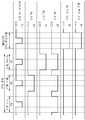
- 제 1 항에 있어서,상기 불소를 제거하는 단계와 상기 수소를 제거하는 단계를 반복 실시하는플라즈마 세정 방법.
- 제 1 항에 있어서,상기 퇴적물을 제거할 때, 불소를 제거할 때 및 수소를 제거할 때에, 각각 플라즈마의 발광을 모니터함으로써 종점 검출하는플라즈마 세정 방법.
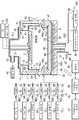
- 제 1 항에 있어서,상기 플라즈마 처리 장치는, 복수의 슬롯을 구비하는 평면 안테나에서 상기 처리 용기 내에 마이크로파를 도입하여 플라즈마를 형성시키며, 피처리 기판 표면에 질화규소막을 퇴적시키는 플라즈마 CVD 장치인플라즈마 세정 방법.
- 복수의 슬롯을 갖는 평면 안테나를 구비한 마이크로파 발생 장치의, 그 내부에 퇴적물이 퇴적하고 있는 처리 용기 내를 세정 가스의 플라즈마를 이용하여 세정하는 플라즈마 세정 방법에 있어서,상기 처리 용기 내에 NF3 가스를 포함하는 세정 가스를 도입하는 단계와,상기 평면 안테나를 통해 마이크로파를 상기 처리 용기 내에 공급함으로써, 상기 처리 용기 내에 상기 세정 가스의 플라즈마를 형성하여 플루오르(F)의 활성종을 생성하는 단계와,상기 처리 용기 내의 상기 퇴적물과 상기 플루오르의 활성종을 반응시켜서 상기 퇴적물을 휘발시키는 단계와,상기 휘발한 퇴적물 성분을 상기 처리 용기로부터 배출시키는 단계와,상기 휘발한 퇴적물 성분의 배출 후에, 상기 처리 용기 내에 수소 가스를 포함하는 가스를 도입하고 플라즈마를 형성하여 상기 처리 용기 내에 잔류하는 불소를 제거하는 단계와,불소를 제거한 후, 상기 처리 용기 내에 희가스를 포함하는 가스를 도입하고 플라즈마를 형성하여 상기 처리 용기 내에 잔류하는 수소를 제거하는 단계를 포함하는플라즈마 세정 방법.
- 삭제
- 플라즈마 CVD 장치의 처리 용기 내에서 피처리 기판의 표면에 질화규소막을 퇴적시키는 플라즈마 CVD 방법에 있어서,상기 처리 용기 내에 도입한 질소 함유 가스와 규소 함유 가스를 포함하는 가스에 의해 플라즈마를 형성하고, 그 플라즈마에 의해 피처리 기판의 표면에 질화규소막을 퇴적시키는 단계와,상기 처리 용기 내에 NF3 가스를 포함하는 세정 가스를 도입하고 플라즈마를 형성하여 상기 처리 용기 내의 퇴적물을 제거하는 단계와,상기 퇴적물을 제거한 후, 상기 처리 용기 내에 수소 가스를 포함하는 가스를 도입하고 플라즈마를 형성하여 상기 처리 용기 내에 잔류하는 불소를 제거하는 단계와,불소를 제거한 후, 또한 상기 처리 용기 내에 희가스를 포함하는 가스를 도입하고 플라즈마를 형성하여 상기 처리 용기 내에 잔류하는 수소를 제거하는 단계를 포함하는플라즈마 CVD 방법.
- 제 8 항에 있어서,상기 불소를 제거하는 단계와 상기 수소를 제거하는 단계를 반복 실시하는플라즈마 CVD 방법.
- 제 8 항에 있어서,수소를 제거한 후, 다시 상기 플라즈마 공정을 실행하는플라즈마 CVD 방법.
- 컴퓨터 상에서 작동하며, 플라즈마 처리 장치의 처리 용기 내를 세정 가스의 플라즈마를 이용하여 세정할 때에 상기 플라즈마 처리 장치를 제어하는 프로그램이 기억된 기억 매체에 있어서,상기 프로그램은, 실행시에,상기 처리 용기 내에 NF3 가스를 포함하는 세정 가스를 도입하고 플라즈마를 형성하여 상기 처리 용기 내의 퇴적물을 제거하는 단계와, 상기 퇴적물을 제거한 후, 상기 처리 용기 내에 수소 가스를 포함하는 가스를 도입하고 플라즈마를 형성하여 상기 처리 용기 내에 잔류하는 불소를 제거하는 단계와, 불소를 제거한 후, 상기 처리 용기 내에 희가스를 포함하는 가스를 도입하고 플라즈마를 형성하여 상기 처리 용기 내에 잔류하는 수소를 제거하는 단계를 포함하는 플라즈마 세정 방법이 실행되도록 컴퓨터로 상기 플라즈마 처리 장치를 제어시키는기억 매체.
- 플라즈마 처리 장치에 있어서,플라즈마를 이용하여 피처리 기판을 처리하기 위한 진공 배기 가능한 처리 용기와,상기 처리 용기 내에 마이크로파를 도입하는 복수의 슬롯을 구비하는 평면 안테나와,상기 처리 용기 내에 세정 가스를 공급하는 가스 공급 기구와,상기 처리 용기 내에 NF3 가스를 포함하는 세정 가스를 도입하고 플라즈마를 형성하여 상기 처리 용기 내의 퇴적물을 제거하는 단계와, 상기 퇴적물을 제거한 후, 상기 처리 용기 내에 수소 가스를 포함하는 가스를 도입하고 플라즈마를 형성하여 상기 처리 용기 내에 잔류하는 불소를 제거하는 단계와, 불소를 제거한 후, 상기 처리 용기 내에 희가스를 포함하는 가스를 도입하고 플라즈마를 형성하여 상기 처리 용기 내에 잔류하는 수소를 제거하는 단계를 포함하는 플라즈마 세정 방법이 실행되도록 각 구성부를 제어하는 제어부를 구비하는플라즈마 처리 장치.
Applications Claiming Priority (3)
| Application Number | Priority Date | Filing Date | Title |
|---|---|---|---|
| JPJP-P-2006-252446 | 2006-09-19 | ||
| JP2006252446 | 2006-09-19 | ||
| PCT/JP2007/068098WO2008035678A1 (en) | 2006-09-19 | 2007-09-18 | Plasma cleaning process and plasma cvd method |
Publications (2)
| Publication Number | Publication Date |
|---|---|
| KR20090053823A KR20090053823A (ko) | 2009-05-27 |
| KR101057877B1true KR101057877B1 (ko) | 2011-08-19 |
Family
ID=39200503
Family Applications (1)
| Application Number | Title | Priority Date | Filing Date |
|---|---|---|---|
| KR1020097005392AActiveKR101057877B1 (ko) | 2006-09-19 | 2007-09-18 | 플라즈마 세정 방법 및 플라즈마 cvd 방법 |
Country Status (6)
| Country | Link |
|---|---|
| US (1) | US8366953B2 (ko) |
| JP (1) | JP5241499B2 (ko) |
| KR (1) | KR101057877B1 (ko) |
| CN (1) | CN101517713B (ko) |
| TW (1) | TWI428962B (ko) |
| WO (1) | WO2008035678A1 (ko) |
Families Citing this family (89)
| Publication number | Priority date | Publication date | Assignee | Title |
|---|---|---|---|---|
| US20110256734A1 (en) | 2010-04-15 | 2011-10-20 | Hausmann Dennis M | Silicon nitride films and methods |
| US9892917B2 (en) | 2010-04-15 | 2018-02-13 | Lam Research Corporation | Plasma assisted atomic layer deposition of multi-layer films for patterning applications |
| US8956983B2 (en) | 2010-04-15 | 2015-02-17 | Novellus Systems, Inc. | Conformal doping via plasma activated atomic layer deposition and conformal film deposition |
| US9997357B2 (en) | 2010-04-15 | 2018-06-12 | Lam Research Corporation | Capped ALD films for doping fin-shaped channel regions of 3-D IC transistors |
| US8637411B2 (en) | 2010-04-15 | 2014-01-28 | Novellus Systems, Inc. | Plasma activated conformal dielectric film deposition |
| US9076646B2 (en) | 2010-04-15 | 2015-07-07 | Lam Research Corporation | Plasma enhanced atomic layer deposition with pulsed plasma exposure |
| US9373500B2 (en) | 2014-02-21 | 2016-06-21 | Lam Research Corporation | Plasma assisted atomic layer deposition titanium oxide for conformal encapsulation and gapfill applications |
| US9257274B2 (en) | 2010-04-15 | 2016-02-09 | Lam Research Corporation | Gapfill of variable aspect ratio features with a composite PEALD and PECVD method |
| US9611544B2 (en) | 2010-04-15 | 2017-04-04 | Novellus Systems, Inc. | Plasma activated conformal dielectric film deposition |
| US9390909B2 (en) | 2013-11-07 | 2016-07-12 | Novellus Systems, Inc. | Soft landing nanolaminates for advanced patterning |
| US9685320B2 (en) | 2010-09-23 | 2017-06-20 | Lam Research Corporation | Methods for depositing silicon oxide |
| US10658161B2 (en)* | 2010-10-15 | 2020-05-19 | Applied Materials, Inc. | Method and apparatus for reducing particle defects in plasma etch chambers |
| US8647993B2 (en) | 2011-04-11 | 2014-02-11 | Novellus Systems, Inc. | Methods for UV-assisted conformal film deposition |
| JP5660205B2 (ja)* | 2011-04-25 | 2015-01-28 | 東京エレクトロン株式会社 | 成膜方法 |
| US8912096B2 (en)* | 2011-04-28 | 2014-12-16 | Applied Materials, Inc. | Methods for precleaning a substrate prior to metal silicide fabrication process |
| JP5659079B2 (ja)* | 2011-05-10 | 2015-01-28 | 株式会社アルバック | ZrBO膜の形成装置 |
| CN103035466B (zh)* | 2011-10-08 | 2016-06-08 | 北京北方微电子基地设备工艺研究中心有限责任公司 | 一种预清洗方法及等离子体设备 |
| US8592328B2 (en) | 2012-01-20 | 2013-11-26 | Novellus Systems, Inc. | Method for depositing a chlorine-free conformal sin film |
| JP6255335B2 (ja)* | 2012-03-22 | 2017-12-27 | 株式会社日立国際電気 | 半導体装置の製造方法、基板処理方法、基板処理装置およびプログラム |
| KR101965256B1 (ko)* | 2012-10-17 | 2019-04-04 | 삼성디스플레이 주식회사 | 유기 발광 표시 장치 |
| KR102207992B1 (ko) | 2012-10-23 | 2021-01-26 | 램 리써치 코포레이션 | 서브-포화된 원자층 증착 및 등각막 증착 |
| SG2013083241A (en) | 2012-11-08 | 2014-06-27 | Novellus Systems Inc | Conformal film deposition for gapfill |
| JP6538300B2 (ja) | 2012-11-08 | 2019-07-03 | ノベラス・システムズ・インコーポレーテッドNovellus Systems Incorporated | 感受性基材上にフィルムを蒸着するための方法 |
| US9246133B2 (en)* | 2013-04-12 | 2016-01-26 | Semiconductor Energy Laboratory Co., Ltd. | Light-emitting module, light-emitting panel, and light-emitting device |
| CN104233234A (zh)* | 2013-06-17 | 2014-12-24 | 沙嫣 | 一种带氟清理装置的pecvd炉及其氟清理方法 |
| US9362163B2 (en)* | 2013-07-30 | 2016-06-07 | Lam Research Corporation | Methods and apparatuses for atomic layer cleaning of contacts and vias |
| US9214334B2 (en) | 2014-02-18 | 2015-12-15 | Lam Research Corporation | High growth rate process for conformal aluminum nitride |
| US9478438B2 (en) | 2014-08-20 | 2016-10-25 | Lam Research Corporation | Method and apparatus to deposit pure titanium thin film at low temperature using titanium tetraiodide precursor |
| US9478411B2 (en) | 2014-08-20 | 2016-10-25 | Lam Research Corporation | Method to tune TiOx stoichiometry using atomic layer deposited Ti film to minimize contact resistance for TiOx/Ti based MIS contact scheme for CMOS |
| US9214333B1 (en) | 2014-09-24 | 2015-12-15 | Lam Research Corporation | Methods and apparatuses for uniform reduction of the in-feature wet etch rate of a silicon nitride film formed by ALD |
| CN105448659A (zh)* | 2014-09-25 | 2016-03-30 | 中芯国际集成电路制造(上海)有限公司 | 一种提高清洗效率的方法 |
| US9640371B2 (en)* | 2014-10-20 | 2017-05-02 | Lam Research Corporation | System and method for detecting a process point in multi-mode pulse processes |
| US9589790B2 (en) | 2014-11-24 | 2017-03-07 | Lam Research Corporation | Method of depositing ammonia free and chlorine free conformal silicon nitride film |
| US9564312B2 (en) | 2014-11-24 | 2017-02-07 | Lam Research Corporation | Selective inhibition in atomic layer deposition of silicon-containing films |
| US10566187B2 (en) | 2015-03-20 | 2020-02-18 | Lam Research Corporation | Ultrathin atomic layer deposition film accuracy thickness control |
| US9828672B2 (en) | 2015-03-26 | 2017-11-28 | Lam Research Corporation | Minimizing radical recombination using ALD silicon oxide surface coating with intermittent restoration plasma |
| JP6524753B2 (ja)* | 2015-03-30 | 2019-06-05 | 東京エレクトロン株式会社 | プラズマ処理装置、プラズマ処理方法及び記憶媒体 |
| US9502238B2 (en) | 2015-04-03 | 2016-11-22 | Lam Research Corporation | Deposition of conformal films by atomic layer deposition and atomic layer etch |
| JP6661283B2 (ja)* | 2015-05-14 | 2020-03-11 | 東京エレクトロン株式会社 | クリーニング方法及びプラズマ処理方法 |
| KR20170002764A (ko) | 2015-06-29 | 2017-01-09 | 삼성전자주식회사 | 반도체 소자의 제조 방법 |
| US10526701B2 (en) | 2015-07-09 | 2020-01-07 | Lam Research Corporation | Multi-cycle ALD process for film uniformity and thickness profile modulation |
| US9601693B1 (en) | 2015-09-24 | 2017-03-21 | Lam Research Corporation | Method for encapsulating a chalcogenide material |
| KR102058106B1 (ko)* | 2015-11-20 | 2019-12-20 | 주식회사 원익아이피에스 | 반도체 소자의 제조방법 |
| CN105714270A (zh)* | 2016-04-15 | 2016-06-29 | 信利(惠州)智能显示有限公司 | 化学气相沉积清洗终点监测方法及其系统 |
| US9773643B1 (en) | 2016-06-30 | 2017-09-26 | Lam Research Corporation | Apparatus and method for deposition and etch in gap fill |
| US10062563B2 (en) | 2016-07-01 | 2018-08-28 | Lam Research Corporation | Selective atomic layer deposition with post-dose treatment |
| US10629435B2 (en) | 2016-07-29 | 2020-04-21 | Lam Research Corporation | Doped ALD films for semiconductor patterning applications |
| US10074543B2 (en) | 2016-08-31 | 2018-09-11 | Lam Research Corporation | High dry etch rate materials for semiconductor patterning applications |
| US10037884B2 (en) | 2016-08-31 | 2018-07-31 | Lam Research Corporation | Selective atomic layer deposition for gapfill using sacrificial underlayer |
| US9865455B1 (en) | 2016-09-07 | 2018-01-09 | Lam Research Corporation | Nitride film formed by plasma-enhanced and thermal atomic layer deposition process |
| CN106373868B (zh)* | 2016-10-10 | 2020-03-10 | 昆山龙腾光电股份有限公司 | 一种阵列基板的制造方法 |
| US10832908B2 (en) | 2016-11-11 | 2020-11-10 | Lam Research Corporation | Self-aligned multi-patterning process flow with ALD gapfill spacer mask |
| US10454029B2 (en) | 2016-11-11 | 2019-10-22 | Lam Research Corporation | Method for reducing the wet etch rate of a sin film without damaging the underlying substrate |
| US10134579B2 (en) | 2016-11-14 | 2018-11-20 | Lam Research Corporation | Method for high modulus ALD SiO2 spacer |
| US10566212B2 (en) | 2016-12-19 | 2020-02-18 | Lam Research Corporation | Designer atomic layer etching |
| US10600624B2 (en) | 2017-03-10 | 2020-03-24 | Applied Materials, Inc. | System and method for substrate processing chambers |
| US10636628B2 (en) | 2017-09-11 | 2020-04-28 | Applied Materials, Inc. | Method for cleaning a process chamber |
| US10312076B2 (en) | 2017-03-10 | 2019-06-04 | Applied Materials, Inc. | Application of bottom purge to increase clean efficiency |
| US10269559B2 (en) | 2017-09-13 | 2019-04-23 | Lam Research Corporation | Dielectric gapfill of high aspect ratio features utilizing a sacrificial etch cap layer |
| JP6845773B2 (ja) | 2017-09-15 | 2021-03-24 | 株式会社日立ハイテク | プラズマ処理方法 |
| JP2021506126A (ja) | 2017-12-07 | 2021-02-18 | ラム リサーチ コーポレーションLam Research Corporation | チャンバ調整における耐酸化保護層 |
| US10760158B2 (en) | 2017-12-15 | 2020-09-01 | Lam Research Corporation | Ex situ coating of chamber components for semiconductor processing |
| CN112005343B (zh) | 2018-03-02 | 2025-05-06 | 朗姆研究公司 | 使用水解的选择性沉积 |
| US12272527B2 (en) | 2018-05-09 | 2025-04-08 | Asm Ip Holding B.V. | Apparatus for use with hydrogen radicals and method of using same |
| KR20250110938A (ko) | 2018-10-19 | 2025-07-21 | 램 리써치 코포레이션 | 반도체 프로세싱을 위한 챔버 컴포넌트들의 인 시츄 (in situ) 보호 코팅 |
| JP2020077750A (ja)* | 2018-11-07 | 2020-05-21 | 東京エレクトロン株式会社 | クリーニング方法及び成膜方法 |
| JP7190915B2 (ja)* | 2019-01-18 | 2022-12-16 | 東京エレクトロン株式会社 | 基板処理装置の洗浄方法、および基板処理装置 |
| KR102726216B1 (ko) | 2019-05-01 | 2024-11-04 | 램 리써치 코포레이션 | 변조된 원자 층 증착 |
| KR102837863B1 (ko) | 2019-06-04 | 2025-07-23 | 램 리써치 코포레이션 | 패터닝시 반응성 이온 에칭을 위한 중합 보호 라이너 |
| JP2022534793A (ja) | 2019-06-07 | 2022-08-03 | ラム リサーチ コーポレーション | 原子層堆積時における膜特性の原位置制御 |
| JP7241627B2 (ja)* | 2019-07-05 | 2023-03-17 | 東京エレクトロン株式会社 | クリーニング方法及びプラズマ処理装置 |
| CN114207184A (zh) | 2019-08-06 | 2022-03-18 | 朗姆研究公司 | 含硅膜的热原子层沉积 |
| JP7257918B2 (ja)* | 2019-08-29 | 2023-04-14 | 東京エレクトロン株式会社 | プラズマ処理システムおよびプラズマ着火支援方法 |
| JP7385809B2 (ja)* | 2019-09-05 | 2023-11-24 | 日新イオン機器株式会社 | イオンビーム照射装置のクリーニング方法 |
| CN110747450A (zh)* | 2019-09-12 | 2020-02-04 | 常州比太科技有限公司 | 一种hit镀膜设备在线清洗后腔体寿命快速恢复方法 |
| JP7398915B2 (ja)* | 2019-10-01 | 2023-12-15 | 東京エレクトロン株式会社 | 基板処理方法、半導体デバイスの製造方法、及び、プラズマ処理装置 |
| CN115735261A (zh) | 2020-07-28 | 2023-03-03 | 朗姆研究公司 | 含硅膜中的杂质减量 |
| CN114551201B (zh)* | 2020-11-24 | 2025-04-25 | 新奥科技发展有限公司 | 一种托卡马克核聚变装置中硼膜的去除方法 |
| JP7489905B2 (ja)* | 2020-11-30 | 2024-05-24 | 東京エレクトロン株式会社 | チャンバーコンディションの診断方法及び基板処理装置 |
| TWI757013B (zh)* | 2020-12-28 | 2022-03-01 | 友達光電股份有限公司 | 控制製程腔室清潔氣體用量的方法及製程處理系統 |
| JP7515419B2 (ja)* | 2021-01-12 | 2024-07-12 | 東京エレクトロン株式会社 | 成膜方法及びプラズマ処理装置 |
| JP7739434B2 (ja) | 2021-02-03 | 2025-09-16 | ラム リサーチ コーポレーション | 原子層エッチングにおけるエッチング選択性の制御 |
| JP2022191960A (ja)* | 2021-06-16 | 2022-12-28 | 東京エレクトロン株式会社 | クリーニング方法及びプラズマ処理装置 |
| JP7713830B2 (ja)* | 2021-08-30 | 2025-07-28 | 東京エレクトロン株式会社 | 成膜方法および成膜装置 |
| KR102843307B1 (ko)* | 2021-12-24 | 2025-08-05 | 세메스 주식회사 | 기판 처리 장치 |
| US20250104981A1 (en)* | 2022-06-08 | 2025-03-27 | Hitachi High-Tech Corporation | Plasma processing method |
| JP2024020777A (ja) | 2022-08-02 | 2024-02-15 | 東京エレクトロン株式会社 | SiN膜の形成方法及びプラズマ処理装置 |
| CN120303440A (zh)* | 2022-12-02 | 2025-07-11 | 朗姆研究公司 | 处理室条件的光谱感测 |
| WO2024166678A1 (ja)* | 2023-02-07 | 2024-08-15 | 東京エレクトロン株式会社 | 成膜方法および基板処理装置 |
Citations (2)
| Publication number | Priority date | Publication date | Assignee | Title |
|---|---|---|---|---|
| JP2001335937A (ja)* | 2000-05-29 | 2001-12-07 | Mitsubishi Heavy Ind Ltd | 金属汚染低減方法及びプラズマ装置の再生方法 |
| JP2002371360A (ja)* | 2001-06-15 | 2002-12-26 | Matsushita Electric Ind Co Ltd | 半導体の製造方法 |
Family Cites Families (18)
| Publication number | Priority date | Publication date | Assignee | Title |
|---|---|---|---|---|
| US5207836A (en)* | 1989-08-25 | 1993-05-04 | Applied Materials, Inc. | Cleaning process for removal of deposits from the susceptor of a chemical vapor deposition apparatus |
| JPH03130368A (ja)* | 1989-09-22 | 1991-06-04 | Applied Materials Inc | 半導体ウェーハプロセス装置の洗浄方法 |
| US5201990A (en)* | 1991-05-23 | 1993-04-13 | Applied Materials, Inc. | Process for treating aluminum surfaces in a vacuum apparatus |
| US5326723A (en)* | 1992-09-09 | 1994-07-05 | Intel Corporation | Method for improving stability of tungsten chemical vapor deposition |
| JPH0732141B2 (ja)* | 1992-09-11 | 1995-04-10 | 株式会社半導体エネルギー研究所 | 炭素膜作製方法 |
| JPH0793276B2 (ja) | 1993-12-14 | 1995-10-09 | アプライド マテリアルズ インコーポレイテッド | 薄膜形成前処理方法および薄膜形成方法 |
| US6200412B1 (en)* | 1996-02-16 | 2001-03-13 | Novellus Systems, Inc. | Chemical vapor deposition system including dedicated cleaning gas injection |
| US7515264B2 (en) | 1999-06-15 | 2009-04-07 | Tokyo Electron Limited | Particle-measuring system and particle-measuring method |
| JP2003037105A (ja) | 2001-07-26 | 2003-02-07 | Tokyo Electron Ltd | プラズマ処理装置及び方法 |
| JP4374854B2 (ja)* | 2001-12-25 | 2009-12-02 | 東京エレクトロン株式会社 | 処理装置及びそのクリーニング方法 |
| US6911233B2 (en)* | 2002-08-08 | 2005-06-28 | Toppoly Optoelectronics Corp. | Method for depositing thin film using plasma chemical vapor deposition |
| JP3657942B2 (ja)* | 2003-01-16 | 2005-06-08 | 沖電気工業株式会社 | 半導体製造装置の洗浄方法、及び半導体装置の製造方法 |
| JP2004335789A (ja)* | 2003-05-08 | 2004-11-25 | Tadahiro Omi | 基板処理装置のクリーニング方法 |
| US20050260354A1 (en)* | 2004-05-20 | 2005-11-24 | Varian Semiconductor Equipment Associates, Inc. | In-situ process chamber preparation methods for plasma ion implantation systems |
| JP2006086325A (ja)* | 2004-09-16 | 2006-03-30 | Tokyo Electron Ltd | クリーニングの終点検出方法 |
| JP4718189B2 (ja)* | 2005-01-07 | 2011-07-06 | 東京エレクトロン株式会社 | プラズマ処理方法 |
| US20070108161A1 (en)* | 2005-11-17 | 2007-05-17 | Applied Materials, Inc. | Chamber components with polymer coatings and methods of manufacture |
| US7510976B2 (en)* | 2006-04-21 | 2009-03-31 | Applied Materials, Inc. | Dielectric plasma etch process with in-situ amorphous carbon mask with improved critical dimension and etch selectivity |
- 2007
- 2007-09-18WOPCT/JP2007/068098patent/WO2008035678A1/jaactiveApplication Filing
- 2007-09-18JPJP2008535357Apatent/JP5241499B2/janot_activeExpired - Fee Related
- 2007-09-18KRKR1020097005392Apatent/KR101057877B1/koactiveActive
- 2007-09-18USUS12/441,828patent/US8366953B2/enactiveActive
- 2007-09-18CNCN2007800347636Apatent/CN101517713B/zhnot_activeExpired - Fee Related
- 2007-09-19TWTW096134906Apatent/TWI428962B/zhnot_activeIP Right Cessation
Patent Citations (2)
| Publication number | Priority date | Publication date | Assignee | Title |
|---|---|---|---|---|
| JP2001335937A (ja)* | 2000-05-29 | 2001-12-07 | Mitsubishi Heavy Ind Ltd | 金属汚染低減方法及びプラズマ装置の再生方法 |
| JP2002371360A (ja)* | 2001-06-15 | 2002-12-26 | Matsushita Electric Ind Co Ltd | 半導体の製造方法 |
Also Published As
| Publication number | Publication date |
|---|---|
| JP5241499B2 (ja) | 2013-07-17 |
| TW200830375A (en) | 2008-07-16 |
| US8366953B2 (en) | 2013-02-05 |
| KR20090053823A (ko) | 2009-05-27 |
| US20090308840A1 (en) | 2009-12-17 |
| CN101517713A (zh) | 2009-08-26 |
| TWI428962B (zh) | 2014-03-01 |
| WO2008035678A1 (en) | 2008-03-27 |
| JPWO2008035678A1 (ja) | 2010-01-28 |
| CN101517713B (zh) | 2011-02-09 |
Similar Documents
| Publication | Publication Date | Title |
|---|---|---|
| KR101057877B1 (ko) | 플라즈마 세정 방법 및 플라즈마 cvd 방법 | |
| JP4836780B2 (ja) | 基板処理装置における処理室のクリーニング方法およびクリーニングの終点検出方法 | |
| US7959970B2 (en) | System and method of removing chamber residues from a plasma processing system in a dry cleaning process | |
| US8747686B2 (en) | Methods of end point detection for substrate fabrication processes | |
| JP4979575B2 (ja) | 基板の窒化処理方法および絶縁膜の形成方法 | |
| KR100978966B1 (ko) | 기판 처리 방법 및 기판 처리 장치 | |
| US7588036B2 (en) | Chamber clean method using remote and in situ plasma cleaning systems | |
| JP2005163183A (ja) | 基板処理装置のクリーニング方法 | |
| JPH1171680A (ja) | 基板処理装置と共に用いるための改良型遠隔マイクロ波プラズマソース用装置 | |
| US20050211264A1 (en) | Method and processing system for plasma-enhanced cleaning of system components | |
| KR101477831B1 (ko) | 플라즈마 질화 처리에 있어서의 챔버 내의 전처리 방법, 플라즈마 처리 방법, 및 플라즈마 처리 장치 | |
| JP5425361B2 (ja) | プラズマ表面処理方法、プラズマ処理方法およびプラズマ処理装置 | |
| WO2009123049A1 (ja) | 高ストレス薄膜の成膜方法及び半導体集積回路装置の製造方法 | |
| JP2889191B2 (ja) | ドライエッチング方法 | |
| JP2025131172A (ja) | プラズマ処理方法及びプラズマ処理装置 | |
| JP2011029250A (ja) | マイクロ波プラズマ処理装置およびマイクロ波プラズマ処理方法 |
Legal Events
| Date | Code | Title | Description |
|---|---|---|---|
| A201 | Request for examination | ||
| PA0105 | International application | St.27 status event code:A-0-1-A10-A15-nap-PA0105 | |
| PA0201 | Request for examination | St.27 status event code:A-1-2-D10-D11-exm-PA0201 | |
| PG1501 | Laying open of application | St.27 status event code:A-1-1-Q10-Q12-nap-PG1501 | |
| E902 | Notification of reason for refusal | ||
| PE0902 | Notice of grounds for rejection | St.27 status event code:A-1-2-D10-D21-exm-PE0902 | |
| R17-X000 | Change to representative recorded | St.27 status event code:A-3-3-R10-R17-oth-X000 | |
| E13-X000 | Pre-grant limitation requested | St.27 status event code:A-2-3-E10-E13-lim-X000 | |
| P11-X000 | Amendment of application requested | St.27 status event code:A-2-2-P10-P11-nap-X000 | |
| P13-X000 | Application amended | St.27 status event code:A-2-2-P10-P13-nap-X000 | |
| E701 | Decision to grant or registration of patent right | ||
| PE0701 | Decision of registration | St.27 status event code:A-1-2-D10-D22-exm-PE0701 | |
| GRNT | Written decision to grant | ||
| PR0701 | Registration of establishment | St.27 status event code:A-2-4-F10-F11-exm-PR0701 | |
| PR1002 | Payment of registration fee | St.27 status event code:A-2-2-U10-U12-oth-PR1002 Fee payment year number:1 | |
| PG1601 | Publication of registration | St.27 status event code:A-4-4-Q10-Q13-nap-PG1601 | |
| FPAY | Annual fee payment | Payment date:20140721 Year of fee payment:4 | |
| PR1001 | Payment of annual fee | St.27 status event code:A-4-4-U10-U11-oth-PR1001 Fee payment year number:4 | |
| FPAY | Annual fee payment | Payment date:20150716 Year of fee payment:5 | |
| PR1001 | Payment of annual fee | St.27 status event code:A-4-4-U10-U11-oth-PR1001 Fee payment year number:5 | |
| FPAY | Annual fee payment | Payment date:20160721 Year of fee payment:6 | |
| PR1001 | Payment of annual fee | St.27 status event code:A-4-4-U10-U11-oth-PR1001 Fee payment year number:6 | |
| FPAY | Annual fee payment | Payment date:20170720 Year of fee payment:7 | |
| PR1001 | Payment of annual fee | St.27 status event code:A-4-4-U10-U11-oth-PR1001 Fee payment year number:7 | |
| FPAY | Annual fee payment | Payment date:20180801 Year of fee payment:8 | |
| PR1001 | Payment of annual fee | St.27 status event code:A-4-4-U10-U11-oth-PR1001 Fee payment year number:8 | |
| FPAY | Annual fee payment | Payment date:20190730 Year of fee payment:9 | |
| PR1001 | Payment of annual fee | St.27 status event code:A-4-4-U10-U11-oth-PR1001 Fee payment year number:9 | |
| PR1001 | Payment of annual fee | St.27 status event code:A-4-4-U10-U11-oth-PR1001 Fee payment year number:10 | |
| PR1001 | Payment of annual fee | St.27 status event code:A-4-4-U10-U11-oth-PR1001 Fee payment year number:11 | |
| PR1001 | Payment of annual fee | St.27 status event code:A-4-4-U10-U11-oth-PR1001 Fee payment year number:12 | |
| PR1001 | Payment of annual fee | St.27 status event code:A-4-4-U10-U11-oth-PR1001 Fee payment year number:13 | |
| PR1001 | Payment of annual fee | St.27 status event code:A-4-4-U10-U11-oth-PR1001 Fee payment year number:14 | |
| PR1001 | Payment of annual fee | St.27 status event code:A-4-4-U10-U11-oth-PR1001 Fee payment year number:15 |