KR101054703B1 - Structure and method for forming asymmetric overlap capacitance in field effect transistor - Google Patents
Structure and method for forming asymmetric overlap capacitance in field effect transistorDownload PDFInfo
- Publication number
- KR101054703B1 KR101054703B1KR1020087009971AKR20087009971AKR101054703B1KR 101054703 B1KR101054703 B1KR 101054703B1KR 1020087009971 AKR1020087009971 AKR 1020087009971AKR 20087009971 AKR20087009971 AKR 20087009971AKR 101054703 B1KR101054703 B1KR 101054703B1
- Authority
- KR
- South Korea
- Prior art keywords
- spacer
- structures
- gate
- offset spacers
- pair
- Prior art date
- Legal status (The legal status is an assumption and is not a legal conclusion. Google has not performed a legal analysis and makes no representation as to the accuracy of the status listed.)
- Expired - Fee Related
Links
Images


Classifications
- H—ELECTRICITY
- H10—SEMICONDUCTOR DEVICES; ELECTRIC SOLID-STATE DEVICES NOT OTHERWISE PROVIDED FOR
- H10D—INORGANIC ELECTRIC SEMICONDUCTOR DEVICES
- H10D84/00—Integrated devices formed in or on semiconductor substrates that comprise only semiconducting layers, e.g. on Si wafers or on GaAs-on-Si wafers
- H10D84/01—Manufacture or treatment
- H10D84/0123—Integrating together multiple components covered by H10D12/00 or H10D30/00, e.g. integrating multiple IGBTs
- H10D84/0126—Integrating together multiple components covered by H10D12/00 or H10D30/00, e.g. integrating multiple IGBTs the components including insulated gates, e.g. IGFETs
- H10D84/013—Manufacturing their source or drain regions, e.g. silicided source or drain regions
- H10D84/0133—Manufacturing common source or drain regions between multiple IGFETs
- H—ELECTRICITY
- H01—ELECTRIC ELEMENTS
- H01L—SEMICONDUCTOR DEVICES NOT COVERED BY CLASS H10
- H01L21/00—Processes or apparatus adapted for the manufacture or treatment of semiconductor or solid state devices or of parts thereof
- H01L21/02—Manufacture or treatment of semiconductor devices or of parts thereof
- H01L21/04—Manufacture or treatment of semiconductor devices or of parts thereof the devices having potential barriers, e.g. a PN junction, depletion layer or carrier concentration layer
- H01L21/18—Manufacture or treatment of semiconductor devices or of parts thereof the devices having potential barriers, e.g. a PN junction, depletion layer or carrier concentration layer the devices having semiconductor bodies comprising elements of Group IV of the Periodic Table or AIIIBV compounds with or without impurities, e.g. doping materials
- H01L21/26—Bombardment with radiation
- H01L21/263—Bombardment with radiation with high-energy radiation
- H01L21/265—Bombardment with radiation with high-energy radiation producing ion implantation
- H01L21/26586—Bombardment with radiation with high-energy radiation producing ion implantation characterised by the angle between the ion beam and the crystal planes or the main crystal surface
- H—ELECTRICITY
- H10—SEMICONDUCTOR DEVICES; ELECTRIC SOLID-STATE DEVICES NOT OTHERWISE PROVIDED FOR
- H10D—INORGANIC ELECTRIC SEMICONDUCTOR DEVICES
- H10D30/00—Field-effect transistors [FET]
- H10D30/01—Manufacture or treatment
- H10D30/021—Manufacture or treatment of FETs having insulated gates [IGFET]
- H10D30/0221—Manufacture or treatment of FETs having insulated gates [IGFET] having asymmetry in the channel direction, e.g. lateral high-voltage MISFETs having drain offset region or extended-drain MOSFETs [EDMOS]
- H—ELECTRICITY
- H10—SEMICONDUCTOR DEVICES; ELECTRIC SOLID-STATE DEVICES NOT OTHERWISE PROVIDED FOR
- H10D—INORGANIC ELECTRIC SEMICONDUCTOR DEVICES
- H10D30/00—Field-effect transistors [FET]
- H10D30/01—Manufacture or treatment
- H10D30/021—Manufacture or treatment of FETs having insulated gates [IGFET]
- H10D30/0223—Manufacture or treatment of FETs having insulated gates [IGFET] having source and drain regions or source and drain extensions self-aligned to sides of the gate
- H10D30/0227—Manufacture or treatment of FETs having insulated gates [IGFET] having source and drain regions or source and drain extensions self-aligned to sides of the gate having both lightly-doped source and drain extensions and source and drain regions self-aligned to the sides of the gate, e.g. lightly-doped drain [LDD] MOSFET or double-diffused drain [DDD] MOSFET
- H—ELECTRICITY
- H10—SEMICONDUCTOR DEVICES; ELECTRIC SOLID-STATE DEVICES NOT OTHERWISE PROVIDED FOR
- H10D—INORGANIC ELECTRIC SEMICONDUCTOR DEVICES
- H10D30/00—Field-effect transistors [FET]
- H10D30/60—Insulated-gate field-effect transistors [IGFET]
- H10D30/601—Insulated-gate field-effect transistors [IGFET] having lightly-doped drain or source extensions, e.g. LDD IGFETs or DDD IGFETs
- H10D30/603—Insulated-gate field-effect transistors [IGFET] having lightly-doped drain or source extensions, e.g. LDD IGFETs or DDD IGFETs having asymmetry in the channel direction, e.g. lateral high-voltage MISFETs having drain offset region or extended drain IGFETs [EDMOS]
- H—ELECTRICITY
- H10—SEMICONDUCTOR DEVICES; ELECTRIC SOLID-STATE DEVICES NOT OTHERWISE PROVIDED FOR
- H10D—INORGANIC ELECTRIC SEMICONDUCTOR DEVICES
- H10D64/00—Electrodes of devices having potential barriers
- H10D64/01—Manufacture or treatment
- H10D64/021—Manufacture or treatment using multiple gate spacer layers, e.g. bilayered sidewall spacers
- H—ELECTRICITY
- H10—SEMICONDUCTOR DEVICES; ELECTRIC SOLID-STATE DEVICES NOT OTHERWISE PROVIDED FOR
- H10D—INORGANIC ELECTRIC SEMICONDUCTOR DEVICES
- H10D84/00—Integrated devices formed in or on semiconductor substrates that comprise only semiconducting layers, e.g. on Si wafers or on GaAs-on-Si wafers
- H10D84/01—Manufacture or treatment
- H10D84/0123—Integrating together multiple components covered by H10D12/00 or H10D30/00, e.g. integrating multiple IGBTs
- H10D84/0126—Integrating together multiple components covered by H10D12/00 or H10D30/00, e.g. integrating multiple IGBTs the components including insulated gates, e.g. IGFETs
- H10D84/0147—Manufacturing their gate sidewall spacers
- H—ELECTRICITY
- H10—SEMICONDUCTOR DEVICES; ELECTRIC SOLID-STATE DEVICES NOT OTHERWISE PROVIDED FOR
- H10D—INORGANIC ELECTRIC SEMICONDUCTOR DEVICES
- H10D84/00—Integrated devices formed in or on semiconductor substrates that comprise only semiconducting layers, e.g. on Si wafers or on GaAs-on-Si wafers
- H10D84/01—Manufacture or treatment
- H10D84/02—Manufacture or treatment characterised by using material-based technologies
- H10D84/03—Manufacture or treatment characterised by using material-based technologies using Group IV technology, e.g. silicon technology or silicon-carbide [SiC] technology
- H10D84/038—Manufacture or treatment characterised by using material-based technologies using Group IV technology, e.g. silicon technology or silicon-carbide [SiC] technology using silicon technology, e.g. SiGe
Landscapes
- Physics & Mathematics (AREA)
- High Energy & Nuclear Physics (AREA)
- Engineering & Computer Science (AREA)
- General Physics & Mathematics (AREA)
- Health & Medical Sciences (AREA)
- Toxicology (AREA)
- Crystallography & Structural Chemistry (AREA)
- Condensed Matter Physics & Semiconductors (AREA)
- Chemical & Material Sciences (AREA)
- Manufacturing & Machinery (AREA)
- Computer Hardware Design (AREA)
- Microelectronics & Electronic Packaging (AREA)
- Power Engineering (AREA)
- Insulated Gate Type Field-Effect Transistor (AREA)
- Metal-Oxide And Bipolar Metal-Oxide Semiconductor Integrated Circuits (AREA)
- Electrodes Of Semiconductors (AREA)
Abstract
Translated fromKoreanDescription
Translated fromKorean본 발명은 일반적으로 반도체 장치 공정 기술에 관한 것으로, 더 상세하게는, 전계 효과 트랜지스터(FET)에 비대칭 오버랩 용량을 형성하는 구조 및 방법에 관한 것이다.TECHNICAL FIELD The present invention generally relates to semiconductor device processing techniques, and more particularly, to a structure and method for forming an asymmetric overlap capacitance in a field effect transistor (FET).
반도체 장치 제조에서, 마이크로프로세서, 메모리 장치 등과 같은 특정 집적 회로 장치의 동작 속도를 증가시키려는 지속적인 흐름이 존재한다. 이러한 흐름은 컴퓨터, 및 점점 증가하는 속도로 동작하는 다른 전자 장치에 대한 소비자 수요에 의해 증폭된다. 증가된 속도에 대한 수요의 결과로서, 트랜지스터와 같은 반도체 장치의 사이즈가 지속적으로 감소해왔다. 예를 들어, 전계 효과 트랜지스터(FET)와 같은 장치에서, 몇 가지 제시해 보자면, 채널 길이, 접합 너비, 및 게이트 유전체 두께와 같은 장치 파라미터는 모두 크기가 계속하여 감소되었다.In semiconductor device manufacturing, there is a constant flow to increase the operating speed of certain integrated circuit devices such as microprocessors, memory devices, and the like. This flow is amplified by consumer demand for computers and other electronic devices operating at increasing speeds. As a result of the demand for increased speed, the size of semiconductor devices such as transistors has continued to decrease. For example, in devices such as field effect transistors (FETs), to some extent, device parameters such as channel length, junction width, and gate dielectric thickness have all continued to decrease in size.
일반적으로 말해서, FET의 채널 길이가 짧아질수록, 트랜지스터는 더 빠르게 동작할 것이다. 또한, 통상적인 트랜지스터 구성요소의 사이즈 및/또는 스케일을 줄임으로써, 주어진 양의 실제 규격의 웨이퍼 상에 생성될 수 있는 트랜지스터의 밀도 및 개수도 증가하므로, 이와 같은 트랜지스터를 병합하는 집적 회로 장치의 비용뿐만 아니라 트랜지스터의 전체 단가를 낮춘다.Generally speaking, the shorter the channel length of the FET, the faster the transistor will operate. In addition, reducing the size and / or scale of conventional transistor components also increases the density and number of transistors that can be produced on a given amount of actual specification wafers, thus reducing the cost of integrated circuit devices incorporating such transistors. In addition, the overall cost of the transistor is lowered.
유감스럽게도, 트랜지스터의 채널 길이를 감소시키는 것은 장채널 트랜지스터에서는 상대적으로 중요하지 않는 "에지 효과"뿐만 아니라 "단채널" 효과까지도 증가시킨다. 다른 측면들 중에서도 단채널 효과의 일례는, 단채널 길이에 대해 확장된 공핍 영역에 기인하여, 트랜지스터가 "오프" 또는 비 전도 상태에 있다고 가정할 때의 증가된 드레인 대 소스 누설 전류를 포함한다. 이와 더불어, 트랜지스터 성능에 역효과를 줄 수 있는 에지 효과들 중 하나가 밀러 용량으로 알려진 것이다. 밀러 용량은 도핑된 다결정 실리콘 게이트 전극, 및 (만약 존재한다면) FET의 고농도 도핑된 소스/드레인 영역 및/또는 저농도 도핑된 소스/드레인 확장(SDE) 영역의 도전성 부분과 (거의 일정하게) 오버랩된 게이트 유전체의 결과로서 발생하는 기생 오버랩 용량(Cov)이다.Unfortunately, reducing the transistor's channel length increases not only the "edge effect" but also the "short channel" effect, which is relatively insignificant in long channel transistors. Among other aspects, an example of a short channel effect includes increased drain to source leakage current when assuming the transistor is in an "off" or non-conducting state due to the depletion region extended over the short channel length. In addition, one of the edge effects that can adversely affect transistor performance is known as the Miller capacitance. Miller capacitance overlaps (almost consistently) the doped polycrystalline silicon gate electrode and the conductive portion of the heavily doped source / drain region and / or the lightly doped source / drain extension (SDE) region of the FET (if present). Parasitic overlap capacitance Cov that occurs as a result of the gate dielectric.
또한, 트랜지스터 치수가 계속하여 줄어들기 때문에, 구동 전류가 유지될 수 있도록 게이트 대 소스/드레인 확장 오버랩은 상대적으로 일정하게 유지될 필요가 있다. 예를 들어, 최소 약 20 nm/side의 오버랩은 트랜지스터 구동 전류(Idsat) 강하를 방지하는데 필수적이다. 오버랩이 너무 작은 경우, 고저항 영역이 확장부와 채널 사이에 생성될 것이다. 장치가 더 작아지면서, 소스 확장 대 드레인 확장 거리는 더 좁아지고, 심각한 펀치스루(punchthrough) 문제를 야기한다.In addition, because the transistor dimensions continue to shrink, the gate-to-source / drain extension overlap needs to remain relatively constant so that the drive current can be maintained. For example, an overlap of at least about 20 nm / side is necessary to prevent the transistor drive current (Idsat ) drop. If the overlap is too small, a high resistance region will be created between the extension and the channel. As the device becomes smaller, the source extension to drain extension distances become narrower and cause severe punchthrough problems.
따라서, 장치의 게이트와 소스 사이에 낮은 직렬 저항을 유지하면서, 동시에 단채널 효과, 핫 캐리어 효과, 펀치스루, 및 과도한 게이트 대 드레인 오버랩에 의해 형성되는 기생 밀러 용량과 같은 불리한 결과들을 최소화하는 FET 장치를 제조하는 것이 바람직할 것이다.Thus, while maintaining a low series resistance between the device's gate and source, the FET device minimizes adverse consequences such as short channel effects, hot carrier effects, punchthrough, and parasitic miller capacitance formed by excessive gate to drain overlap. It would be desirable to prepare.
종래 기술에 대해 앞서 논의한 단점 및 결함들은, 반도체 장치용 비대칭 스페이서 구조를 형성하는 방법에 의해 극복되거나 또는 경감된다. 예시적 실시예에서, 이 방법은, 반도체 기판상에 인접하게 이격된 적어도 한 쌍의 게이트 구조상에 스페이서 층을 형성하는 단계를 포함한다. 스페이서 층이 게이트 구조들 사이의 영역에서는 제1 두께로 형성되고 그 외의 영역에서는 상기 제1 두께보다 두꺼운 제2 두께로 형성되도록 게이트 구조가 이격되어 있다. 스페이서 층은 한 쌍의 인접하게 이격된 게이트 구조들에 대해 비대칭 스페이서 구조를 형성하도록 에칭된다.The disadvantages and deficiencies discussed above with respect to the prior art are overcome or alleviated by the method of forming an asymmetric spacer structure for a semiconductor device. In an exemplary embodiment, the method includes forming a spacer layer on at least one pair of gate structures spaced apart adjacent to the semiconductor substrate. The gate structures are spaced apart so that the spacer layer is formed to a first thickness in the region between the gate structures and to a second thickness thicker than the first thickness in the other regions. The spacer layer is etched to form an asymmetric spacer structure with respect to the pair of adjacently spaced gate structures.
다른 실시예에서, 반도체 장치용 전계 효과 트랜지스터(FET) 구조를 형성하는 방법은, 반도체 기판상에 인접하게 이격된 적어도 한 쌍의 게이트 구조를 형성하는 단계, 및 그 인접하게 이격된 게이트 구조들 상에 스페이서 층을 형성하는 단계를 포함한다. 스페이서 층이 게이트 구조들 사이의 영역에서는 제1 두께로 형성되고 그 외의 영역에서는 상기 제1 두께보다 두꺼운 제2 두께로 형성되도록 게이트 구조들이 이격되어 있다. 스페이서 층은 한 쌍의 인접하게 이격된 게이트 구조들의 측벽들과 인접한 비대칭 스페이서 구조를 형성하도록 에칭되고, 기판에는 비대칭 스페이서 구조를 따라 비대칭 특성을 갖는 도핑 영역이 임플란트된다.In another embodiment, a method of forming a field effect transistor (FET) structure for a semiconductor device includes forming at least a pair of adjacently spaced gate structures on a semiconductor substrate, and over the adjacently spaced gate structures. Forming a spacer layer thereon. The gate structures are spaced apart so that the spacer layer is formed to a first thickness in the region between the gate structures and to a second thickness thicker than the first thickness in the other regions. The spacer layer is etched to form an asymmetric spacer structure adjacent to the sidewalls of the pair of adjacently spaced gate structures, and the substrate is implanted with a doped region having asymmetrical properties along the asymmetric spacer structure.
또 다른 실시예에서, 반도체 장치용 전계 효과 트랜지스터(FET) 구조를 형성하는 방법은, 반도체 기판상에 인접하게 이격된 적어도 한 쌍의 게이트 구조를 형성하는 단계, 한 쌍의 인접하게 이격된 게이트 구조들의 측벽들과 인접한 오프셋 스페이서들을 형성하는 단계, 및 기판에 확장 영역을 형성하는 단계를 포함한다. 제2 스페이서 층은 오프셋 스페이서, 게이트 구조, 및 기판상에 형성된다. 제2 스페이서 층에는, 중성 종의 단일 경사 이온 주입이 행해지는데, 이 이온 주입은 한 방향에서 행해진다. 제2 스페이서 층은 에칭되는데, 상기 단일 경사 이온 주입이 행해진 제2 스페이서 층의 일부는 제2 스페이서 층의 노출되지 않은 부분들보다 빠르게 에칭되므로, 오프셋 스페이서들에 인접한 비대칭적인 제2 스페이서들이 형성된다. 그 다음 기판에는 소스 및 드레인 영역이 임플란트된다.In yet another embodiment, a method of forming a field effect transistor (FET) structure for a semiconductor device includes forming at least a pair of adjacently spaced gate structures on a semiconductor substrate, a pair of adjacently spaced gate structures Forming offset spacers adjacent the sidewalls of the substrate, and forming an extension region in the substrate. The second spacer layer is formed on the offset spacer, the gate structure, and the substrate. A single oblique ion implantation of neutral species is performed in the second spacer layer, which is implanted in one direction. The second spacer layer is etched, wherein a portion of the second spacer layer subjected to the single oblique ion implantation is etched faster than the unexposed portions of the second spacer layer, so that asymmetric second spacers adjacent to the offset spacers are formed. . The source and drain regions are then implanted into the substrate.
또 다른 실시예에서, 전계 효과 트랜지스터(FET) 장치는, 반도체 기판상에 형성된 게이트 구조, 게이트 구조의 측벽상에 형성된 한 쌍의 제1 스페이서 구조, 및 한 쌍의 제1 스페이서 구조와 인접하게 형성된 한 쌍의 제2 스페이서 구조를 포함하는데, 상기 한 쌍의 제2 스페이서 구조는 서로에 대해 비대칭인 두께를 갖는다. 소스 영역 및 확장 영역은 게이트 구조의 한 측면 상에 임플란트되고, 드레인 영역 및 확장 영역은 게이트 구조의 다른 측면 상에 임플란트된다. 소스 영역의 확장 영역은, 한 쌍의 제2 스페이서 구조의 비대칭 두께에 따라, 드레인 영역의 확장 영역과는 상이한 길이를 갖는다.In another embodiment, a field effect transistor (FET) device is formed adjacent to a gate structure formed on a semiconductor substrate, a pair of first spacer structures formed on sidewalls of the gate structure, and a pair of first spacer structures. And a pair of second spacer structures, the pair of second spacer structures having a thickness asymmetrical with respect to each other. The source and extension regions are implanted on one side of the gate structure and the drain and extension regions are implanted on the other side of the gate structure. The extended region of the source region has a different length from the extended region of the drain region, depending on the asymmetric thickness of the pair of second spacer structures.
몇몇 도면에서 동일한 요소들이 동일한 번호를 갖는 예시적 도면들을 참고하여 본다.Reference is made to example figures in which some elements have the same number.
도 1 내지 도 3은 본 발명의 예시적 실시예에 따라, FET 장치의 비대칭적 소스 및 드레인 오버랩 영역의 형성을 도시하는 일련의 단면도이다.1-3 are a series of cross-sectional views illustrating the formation of an asymmetric source and drain overlap region of a FET device, in accordance with an exemplary embodiment of the present invention.
도 4 내지 도 7, 및 도 9는 본 발명의 대안적 실시예에 따라, FET 장치의 비대칭적 소스 및 드레인 확장 영역의 형성을 도시한 일련의 단면도이다.4-7, and 9 are a series of cross-sectional views illustrating the formation of an asymmetric source and drain extension region of a FET device, in accordance with alternative embodiments of the present invention.
도 8은 도 7에 도시된 공정 단계에 따라 형성된 장치의 예시적 SEM 이미지이다.8 is an exemplary SEM image of an apparatus formed according to the process steps shown in FIG. 7.
도 10은 비대칭 스페이서들을 갖는 SRAM 셀의 일부에 대한 예시적 SEM 이미지이다.10 is an exemplary SEM image of a portion of an SRAM cell with asymmetric spacers.
도 11 내지 도 14는 본 발명의 대안적 실시예에 따라, FET 장치의 비대칭 소스 및 드레인 오버랩 영역의 형성을 도시한 일련의 단면도이다.11-14 are a series of cross-sectional views illustrating the formation of an asymmetric source and drain overlap region of a FET device, in accordance with an alternative embodiment of the present invention.
도 15 내지 도 20은 본 발명의 또 다른 실시예에 따라, FET 장치의 비대칭 소스 및 드레인 확장 영역의 형성을 도시한 일련의 단면도이다.15-20 are a series of cross-sectional views illustrating the formation of an asymmetric source and drain extension region of a FET device, in accordance with another embodiment of the present invention.
전계 효과 트랜지스터(FET)의 오버랩 용량을 줄이는 방법 및 구조가 개시된다. 종래의 FET 제조 공정에서, 게이트 도체의 대향면들 상에 형성된 스페이서 구조들이 일반적으로 대칭이므로, 연속하여 형성된 소스 및 드레인 확장 영역은 게이트에 대해 동일한 양의 오버랩을 갖는다. 그러나, 트랜지스터 구동 전류는 주로 소스측 오버랩(즉, 게이트 대 소스 저항)의 양에 의해 제어되기 때문에, 드레인 측 오버랩의 양은 구동 전류에 부정적인 영향을 주지 않고서도 감소될 수 있다. 한편, 게이트 대 드레인 오버랩의 감소는, 예컨대, 단채널 효과, 펀치스루, 핫 캐리어 효 과, 및 기생 용량의 점에서 보면 바람직하다.A method and structure for reducing overlap capacity of a field effect transistor (FET) is disclosed. In a conventional FET fabrication process, the spacer structures formed on opposite sides of the gate conductor are generally symmetrical, so that the successively formed source and drain extension regions have the same amount of overlap for the gate. However, since the transistor drive current is primarily controlled by the amount of source side overlap (ie, gate-to-source resistance), the amount of drain side overlap can be reduced without negatively affecting the drive current. On the other hand, the reduction of the gate-to-drain overlap is preferable in view of, for example, the short channel effect, the punchthrough effect, the hot carrier effect, and the parasitic capacitance.
또한, 장치의 치수가 줄어듦에 따라, 확장 저항이 우세하게 된다. 더 짧은 소스측 확장 (좁은 스페이서 너비의 결과로서)은, 드레인측 확장 (스페이서 너비를 줄이지 않은 결과로서)이 적당한 길이로 유지되기 때문에, 핫 캐리어 효과와 같은 문제를 발생시키지 않으면서도 직렬 저항을 감소시키고 장치 성능을 향상시킬 것이다. 이는, 소스 및 드레인 측들에 대해 대칭인 확장 영역을 형성하여, 이어서 대칭 소스 및 드레인 확장 길이를 발생시키는 종래의 방법과는 반대이다.In addition, as the size of the device is reduced, the expansion resistance prevails. Shorter source-side expansion (as a result of narrow spacer widths) reduces series resistance without causing problems such as hot carrier effects, because drain-side expansion (as a result of not reducing the spacer width) is maintained at a reasonable length. And will improve device performance. This is in contrast to the conventional method of forming an extension region symmetrical about the source and drain sides, which in turn generates a symmetrical source and drain extension length.
따라서, 더 상세히 설명되는 바와 같이, 개시되는 본 발명은, 긴 확장 영역 및 짧은 확장 영역뿐만 아니라 긴 오버랩 및 짧은 오버랩을 갖는 소스 및 드레인 확장 영역을 이어서 발생시키는 비대칭 스페이서 구조를 생성하는 다양한 제조 기술을 이용한다.Accordingly, as will be described in more detail, the disclosed invention discloses various fabrication techniques that produce an asymmetric spacer structure that subsequently generates source and drain extension regions with long and short overlap regions as well as long and short overlap regions. I use it.
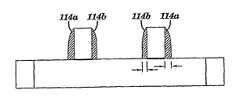
우선 도 1 내지 도 3을 참조하면, 본 발명의 예시적 실시예에 따른 FET 장치(100)의 한 쌍의 비대칭 소스 및 드레인 오버랩 영역의 형성을 나타내는 일련의 단면도들이 도시되어 있다. 특히, 도 1에는 반도체 기판(104)(예컨대, 실리콘) 상에 형성된 한 쌍의 인접한 게이트 도체(102)들이 도시되어 있는데, 게이트(102)들은 대응하는 게이트 산화물 층(106) 상에 형성된다. 기판(104)상에서 개개의 장치를 전기적으로 서로 절연시키기 위한 얕은 트렌치 절연(Shallow Trench Isolation) 구조(108)도 또한 도시되어 있다. 기본 FET 구조들은 당업자들에게 잘 알려져 있기 때문에, STI(108) 및 게이트 산화물 층(106)과 같은 특정 구조물(feature)들은 본 명세서에서 더 상세하기 논의하지 않겠다.Referring first to FIGS. 1-3, a series of cross-sectional views illustrating the formation of a pair of asymmetric source and drain overlap regions of a
도 1에 또한 도시된 바와 같이, 균일하지 않은 두께의 스페이서 층(130)이 한 쌍의 게이트 구조(102) 상에 형성된다. 도 1의 실시예는 매우 근접한 2개의 이웃하는 (예를 들어, 게이트 높이의 약 1 내지 3배에 달하는 게이트 간 분리를 갖는) 게이트들을 이용한다. 스페이서 층(130)을 형성하는데 있어서 증착 파라미터를 선택적으로 조정함으로써, 게이트의 바깥 측 상의 영역들에 비해 더 얇은 막이 2개의 게이트 사이의 영역 상에 형성될 것이다. 이와 같이, 스페이서 층(130)이 패터닝되고 에칭되는 경우, 도 2에 도시된 바와 같이, 균일하지 않은 두께 층의 일정한 에칭율로부터 비대칭한 스페이서들(114a, 114b)이 발생할 것이다.As also shown in FIG. 1, a non-uniform
비대칭 스페이서의 형성에 후속하여, 도 3에는 표준의 장치 공정에 따라 할로 및 확장 주입 단계들이 도시되어 있다. 주입 도펀트 물질들을 주입하도록(drive) 어닐링한 후, 얇은 스페이서(114b)에 대응하는 확장 영역(116)이 두꺼운 스페이서(114a)에 대응하는 확장 영역(118)보다 긴 오버랩을 갖는 것이 보인다. 즉, "긴 오버랩" 확장 영역(116)은 게이트 아래에서 "짧은 오버랩"이 확장 영역(118)이 확장되는 것보다 더 확장된다. 바람직한 실시예에서, FET 구조의 소스 단자는 (구동 전류를 유지하기 위해) 게이트의 긴 오버랩 확장 측면에 위치되지만, 드레인 단자는 (전반적으로 오버랩 용량을 줄이고 단채널 효과를 향상시키기 위해) 게이트의 짧은 오버랩 확장 측면에 위치된다.Subsequent to the formation of the asymmetric spacers, halo and extended implantation steps are shown in accordance with the standard device process. After annealing to inject the implantation dopant materials, it is seen that the
균일하지 않은 층 형성을 통한 비대칭 스페이서 형성의 원리는 깊은 소스 및 드레인 영역의 형성 중에도 적용될 수 있다. 도 4 내지 도 7, 및 도 9는 본 발명의 다른 실시예에 따른 FET 장치의 비대칭 소스 및 드레인 확장 영역의 형성을 나타내 는 일련의 단면도이다. 도 4부터 시작해보면, 오프셋 스페이서(114)는 초기에 FET 게이트 구조상에 형성된다.The principle of asymmetrical spacer formation through non-uniform layer formation can be applied even during the formation of deep source and drain regions. 4-7, and 9 are a series of cross-sectional views illustrating the formation of an asymmetric source and drain extension region of a FET device according to another embodiment of the present invention. Starting from FIG. 4, an offset
스페이서(114)는 종래의 공정대로 대칭일 수 있고(즉, 실질적으로 게이트 양쪽 측면 상에 동일한 두께를 갖는다), 또는 대안으로서, 스페이서(114)는 도 2에 도시된 바와 같이 비대칭으로 형성될 수 있다. 예시를 위해, 오프셋 스페이서(114)는 현 시퀀스에서 대칭으로 도시된다. 도 5에는 주입된 도펀트 물질을 확산시키기 위한 어닐링이 후속하는, 표준의 장치 공정에 따른 할로 및 확장 주입 단계가 도시되어 있다. 대칭 오프셋 스페이서(114)에 대해, 게이트의 양쪽 측면 상의 결과적인 확장 영역(120)은 실질적으로 동일한 오버랩을 가질 것이다. 한편, 스페이서(114)가 도 1-2에 도시된 공정에 따라 형성되는 경우, 비대칭 확장 영역은 도 3에 도시된 바와 같이 나타날 것이다.The
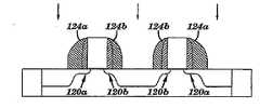
도 6에 도시된 바와 같이, 균일하지 않은 제2 스페이서 층(132) (예컨대, Si3N4)이 장치상에 형성된다. 도 1의 실시예와 유사하게, (게이트 사이의 거리가 충분히 가깝게 주어지고, 공정 조건이 적당히 조절된) 제2 스페이서 층(132)은 게이트 사이의 영역에서는 얇게 형성되고, 게이트 바깥 영역에서는 두껍게 형성될 것이다. 일단 제2 스페이서 층(132)이 도 7에 도시된 것처럼 패터닝되고 에칭되면, 비대칭 스페이서(124a, 124b)가 형성된다. 부차적으로 설명하면, 도 7에 도시된 공정 단계에 따라 형성된 장치의 예시적 SEM 이미지가 도 8에 도시되어 있다.As shown in FIG. 6, a non-uniform second spacer layer 132 (eg, Si3 N4 ) is formed on the device. Similar to the embodiment of FIG. 1, the second spacer layer 132 (given a sufficiently close distance between the gates and appropriately controlled process conditions) is formed thin in the region between the gates and thick in the region outside the gate. Will be. Once the
비대칭 스페이서(124a, 124b)의 형성을 통해, 도 9에 도시된 소스/드레인 이 온 주입 단계는 상이한 길이의 확장을 야기한다. 더 상세하게, 게이트의 바깥 측면 상의 확장 영역(120a)은 게이트 사이의 확장 영역(120b)과 비교하여 더 길다. 이는 제2 세트의 스페이서들이 더 얇을 경우, 깊은 소스/드레인 주입이 게이트에 근접하게 되어, 도 5에서 형성된 확장 영역이 짧아진다는 사실에 기인한다. 이와 같이 확산 영역이 짧아지면, 캐리어(예, 전자 또는 정공)에 대한 저항이 더 낮아진다. 이와 같은 실시예에서, 공통의 소스 단자는 직렬 저항을 줄이기 위해 게이트들 사이에 위치되지만, 드레인 단자는 확산 영역이 더 긴 게이트 바깥에 위치되는 것이 실용적일 것이다.Through the formation of
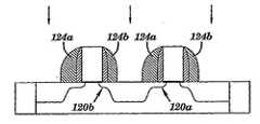
이와 같은 애플리케이션의 한 가지 적합한 예가 SRAM 셀의 PFET 장치 쌍일 수 있는데, 이 장치 쌍 사이에는 전원 전압(VDD)에 접속된 소스 단자들이 있다. 도 10은 도 9에 도시된 실시예와 유사한, 비대칭 스페이서들을 갖는 SRAM 셀의 일부에 대한 예시적 SEM 이미지이다. 설명되는 바와 같이, 얇은 스페이서들이 2개의 게이트 사이에 위치된다.One suitable example of such an application may be a pair of PFET devices in an SRAM cell, with the source terminals connected to the supply voltage VDD. FIG. 10 is an exemplary SEM image of a portion of an SRAM cell with asymmetric spacers, similar to the embodiment shown in FIG. 9. As will be explained, thin spacers are located between the two gates.
도 11 내지 도 14에는 본 발명의 추가 실시예에 따라 비대칭 스페이서들을 형성하는 다른 기술이 도시되어 있다. 앞서 논의한 실시예와 같이, 도 11에는 반도체 기판(104), 게이트 산화물 층(106), 및 STI 구조(108) 상에 형성된 한 쌍의 게이트 도체(102)가 도시되어 있다. 또한, 스페이서 층(110) (예를 들어, 산화물, TEOS, 실리콘 질화물)이 도펀트 주입에 앞서 스페이서를 형성할 목적으로 장치(100) 상에 형성된다.11-14 illustrate another technique for forming asymmetrical spacers in accordance with a further embodiment of the present invention. As in the previously discussed embodiment, FIG. 11 shows a pair of
그 다음, 종래의 방식대로, 도 11의 스페이서 층(110)이 패터닝되고 불균일 에칭되어, 게이트 도체(102)의 측벽을 따라 실질적으로 대칭인 스페이서들이 생긴다. 그러나, 도 12에 도시된 바와 같이, 웨이퍼에는 예컨대, 게르마늄(Ge) 또는 크세논(Xe)과 같은 중성 도펀트 종의 단일 경사 이온 주입 (화살표 112)이 행해진다. 이는 게이트 구조의 한 측면 상에서, 스페이서 층(110)에 단일 경사 이온 주입이 행해지도록 한다. 예시적 실시예에서, 주입 각은 약 10°내지 35°일 수 있다. 이와 같은 주입의 효과는 스페이서 층(110)의 나머지 부분에 비해 주입된 부분의 에칭률을 상승시킨다. 따라서, 도 13에 도시된 바와 같이, 주입된 스페이서 층(110)이 연속하여 패터닝되고 에칭될 때, 각각의 게이트는 한 쌍의 스페이서(114a, 114b)와 함께 남게되고, 여기서 게이트의 주입된 측면 상의 스페이서(114b)는 게이트의 주입되지 않은 측면 상의 스페이서(114a)에 비해 더 얇다(즉, 비대칭이다).Then, in a conventional manner, the
비대칭 스페이서의 형성에 후속하여, 도 14에는 도 3의 구조와 유사한 더 긴 오버랩(116)과 더 짧은 오버랩(118)을 갖는 확장 영역을 형성하기 위한 할로 및 확장 주입 단계가 도시되어 있다. 그러나, 도 3의 더 긴 오버랩(116)이 게이트 내부에 위치되는 반면, 도 14의 더 긴 오버랩(116)은 게이트의 우측면 상에 위치된다.Subsequent to the formation of the asymmetric spacer, FIG. 14 shows a halo and expanded implantation step for forming an extended region having a
이온 주입을 통한 비대칭 스페이서 형성의 원리는 소스 및 드레인 영역의 형성 중에도 적용될 수 있다. 도 15 내지 도 20은 본 발명의 또 다른 실시예에 따라, FET 장치의 비대칭 소스 및 드레인 확장 영역의 형성을 나타내는 일련의 단면도이다. 도 15부터 시작하여 보면, FET 구조는 오프셋 스페이서(114)의 형성 이후인 것으로 도시된 것이다. 도 4와 같이, 오프셋 스페이서(114)는 도 5의 할로/확장 이온 주입 단계에 앞서 대칭으로 형성되거나 또는 비대칭으로 형성될 수 있다.The principle of asymmetric spacer formation through ion implantation can also be applied during the formation of the source and drain regions. 15-20 are a series of cross-sectional views illustrating the formation of an asymmetric source and drain extension region of a FET device, in accordance with another embodiment of the present invention. Starting from FIG. 15, the FET structure is shown after formation of the offset
도 16에는 주입된 도펀트 물질을 확산시키기 위한 어닐링이 후속되는, 표준의 장치 공정에 따른 할로 및 확장 주입 단계가 도시되어 있다. 대칭 오프셋 스페이서에 대해, 게이트의 양쪽 측면 상의 결과 확장 영역(120)은 실질적으로 동일한 오버랩을 가질 것이다. 즉, 스페이서(114)가 도 12-13에 도시된 공정에 따라 형성된다면, 확장 영역(120)은 도 14에 도시된 바와 같이 나타날 것이다. 어느 경우도, 제2 스페이서 층(122)(예컨대, Si3N4)은 도 17에 도시된 바와 같이 장치상에 형성된다.FIG. 16 shows a halo and extended implantation step according to a standard apparatus process, followed by annealing to diffuse the implanted dopant material. For symmetric offset spacers, the resulting
그 다음, 도 18에 도시된 바와 같이, 제2 스페이서 층(122)에는, 앞서 논의한 실시예와 유사한 방식으로, 중성 도펀트 종의 단일 경사 이온 주입(화살표 112)이 행해진다. 다시, 이는 층(122)의 주입된 부분의 에칭률 증가의 효과를 갖는다. 따라서, 층(122)이 도 19에 도시된 바와 같이 패터닝되고 에칭될 때, 제2 세트의 스페이서들(124a, 124b)은 제1 세트의 오프셋 스페이서들(114) 상에 형성된다. 제1 세트의 오프셋 스페이서들(114)이 대칭이건 비대칭이건 간에 상관없이, 제2 세트의 스페이서들은 실제로는 도 18에 도시된 경사진 주입에 기인하여 비대칭일 것이다. 실제로, 게이트 구조의 비-주입된 측면은 두꺼운 스페이서(124a)를 포함하지만, 게이트 구조의 주입된 측면은 얇은 스페이서(124b)를 포함한다.Then, as shown in FIG. 18, the
최종적으로, 도 20에 도시된 바와 같이, 웨이퍼는 종래의 공정 도핑에 따라 (깊은) 소스/드레인 주입을 받는다. 그러나, 얇은 스페이서(124b)에 대응하는 게이트의 측면 상에서, 깊은 소스/드레인 주입 후에 남아있는 결과 확장 영역(120b)의 길이는 두꺼운 스페이서(124a)에 대응하는 게이트의 측면 상의 확장 영역(120a)의 길이보다 짧아진다. 따라서, 바람직한 실시예에서, FET의 소스측은 얇은 스페이서(124b)에 대응하는 게이트의 측면에 위치된다. 반대로, 드레인측의 확장 영역은 핫 캐리어 효과를 방지하기 위해 여전히 특정 길이로 유지된다.Finally, as shown in FIG. 20, the wafer is subjected to (deep) source / drain implantation according to conventional process doping. However, on the side of the gate corresponding to the thin spacer 124b, the length of the resulting extension region 120b remaining after deep source / drain implantation is the length of the
스페이서 층의 에칭률을 증가시키기 위해 중성 종의 도펀트 경사 주입 단계를 이용함으로써, 비대칭 스페이서 두께를 갖는 FET 장치가 달성될 수 있다. 이는 더 길고 더 짧은 확장 영역뿐만 아니라 길고/짧은 오버랩을 갖는 확장을 허용한다. 그러나, 앞서 논의된 바와 같은 비대칭 스페이서를 야기하는 추가의 방법도 고려된다.By using a neutral species dopant gradient implantation step to increase the etch rate of the spacer layer, a FET device with an asymmetric spacer thickness can be achieved. This allows for extensions with long / short overlaps as well as longer and shorter extension areas. However, additional methods of causing asymmetric spacers as discussed above are also contemplated.
본 발명은 바람직한 실시예 또는 실시예들을 참조하여 설명되었지만, 본 발명의 범위를 벗어나지 않고 다양한 변경이 이루어질 수 있고, 등가물들이 본 발명의 구성 요소들을 대신할 수 있다는 것을 당업자들은 이해할 것이다. 또한, 많은 조정이 본 발명의 본질적인 범위를 벗어나지 않고, 특별한 상황이나 물질들이 본 발명의 기술들에 적합하도록 행해질 수 있다. 따라서, 본 명세서는 본 발명을 수행하는데 최상의 모드로 고려되어 개시된 특정 실시예에 본 발명을 한정하지 않지만, 첨부한 청구항들의 범위 내에 있는 모든 실시예들은 포함하는 것으로 의도되었다.Although the present invention has been described with reference to preferred embodiments or embodiments, those skilled in the art will understand that various changes may be made without departing from the scope of the present invention and equivalents may replace the elements of the present invention. In addition, many adjustments may be made to adapt the techniques of the invention without departing from the essential scope thereof. Accordingly, the specification is not intended to limit the invention to the particular embodiments disclosed and considered to be the best mode of carrying out the invention, but it is intended to include all embodiments falling within the scope of the appended claims.
본 발명의 구조 및 방법은 집적 회로, 더 상세하게는 전계 효과 트랜지스터의 제조에 유용하다.The structure and method of the present invention are useful in the manufacture of integrated circuits, and more particularly field effect transistors.
Claims (10)
Translated fromKoreanApplications Claiming Priority (3)
| Application Number | Priority Date | Filing Date | Title |
|---|---|---|---|
| US11/163,165 | 2005-10-07 | ||
| US11/163,165US7396713B2 (en) | 2005-10-07 | 2005-10-07 | Structure and method for forming asymmetrical overlap capacitance in field effect transistors |
| PCT/US2006/038593WO2007044324A2 (en) | 2005-10-07 | 2006-10-02 | Structure and method for forming asymmetrical overlap capacitance in field effect transistors |
Publications (2)
| Publication Number | Publication Date |
|---|---|
| KR20080061378A KR20080061378A (en) | 2008-07-02 |
| KR101054703B1true KR101054703B1 (en) | 2011-08-08 |
Family
ID=37910389
Family Applications (1)
| Application Number | Title | Priority Date | Filing Date |
|---|---|---|---|
| KR1020087009971AExpired - Fee RelatedKR101054703B1 (en) | 2005-10-07 | 2006-10-02 | Structure and method for forming asymmetric overlap capacitance in field effect transistor |
Country Status (7)
| Country | Link |
|---|---|
| US (2) | US7396713B2 (en) |
| EP (1) | EP1946360A4 (en) |
| JP (2) | JP5225091B2 (en) |
| KR (1) | KR101054703B1 (en) |
| CN (1) | CN101647108B (en) |
| TW (1) | TW200731417A (en) |
| WO (1) | WO2007044324A2 (en) |
Families Citing this family (32)
| Publication number | Priority date | Publication date | Assignee | Title |
|---|---|---|---|---|
| JP5170490B2 (en)* | 2005-06-09 | 2013-03-27 | セイコーエプソン株式会社 | Semiconductor device |
| US7915670B2 (en) | 2007-07-16 | 2011-03-29 | International Business Machines Corporation | Asymmetric field effect transistor structure and method |
| US7843016B2 (en)* | 2007-07-16 | 2010-11-30 | International Business Machines Corporation | Asymmetric field effect transistor structure and method |
| US20090159936A1 (en)* | 2007-12-20 | 2009-06-25 | Uday Shah | Device with asymmetric spacers |
| US9016236B2 (en)* | 2008-08-04 | 2015-04-28 | International Business Machines Corporation | Method and apparatus for angular high density plasma chemical vapor deposition |
| DE102008049719A1 (en)* | 2008-09-30 | 2010-04-08 | Advanced Micro Devices, Inc., Sunnyvale | Asymmetric transistor devices made by asymmetric spacers and suitable implantation |
| JP5442235B2 (en)* | 2008-11-06 | 2014-03-12 | ルネサスエレクトロニクス株式会社 | Semiconductor device manufacturing method and semiconductor device |
| US8334560B2 (en)* | 2009-09-02 | 2012-12-18 | Taiwan Semiconductor Manufacturing Company, Ltd. | Reverse disturb immune asymmetrical sidewall floating gate devices |
| US20110049582A1 (en)* | 2009-09-03 | 2011-03-03 | International Business Machines Corporation | Asymmetric source and drain stressor regions |
| US8643107B2 (en)* | 2010-01-07 | 2014-02-04 | International Business Machines Corporation | Body-tied asymmetric N-type field effect transistor |
| US8426917B2 (en)* | 2010-01-07 | 2013-04-23 | International Business Machines Corporation | Body-tied asymmetric P-type field effect transistor |
| CN102446770A (en)* | 2011-10-12 | 2012-05-09 | 上海华力微电子有限公司 | Method and structure for improving writing speed of floating body dynamic random access memory unit |
| CN102543881B (en)* | 2011-11-02 | 2014-08-06 | 上海华力微电子有限公司 | Method for increasing writing speed of floating body cell |
| CN102437124B (en)* | 2011-11-17 | 2014-01-08 | 上海华力微电子有限公司 | Method for increasing writing speed of floating body effect storage unit and semiconductor device |
| CN103187300B (en)* | 2011-12-31 | 2016-02-17 | 中芯国际集成电路制造(上海)有限公司 | Fin formula field effect transistor and forming method thereof |
| CN103247528B (en)* | 2012-02-03 | 2015-09-02 | 中芯国际集成电路制造(上海)有限公司 | The manufacture method of metal oxide semiconductor field effect tube |
| CN102637602A (en)* | 2012-02-28 | 2012-08-15 | 上海华力微电子有限公司 | Method for reducing grid-induction drain leakage of semiconductor device |
| CN102623502A (en)* | 2012-03-23 | 2012-08-01 | 上海华力微电子有限公司 | Common source operational amplifier and manufacturing method thereof |
| CN102610502A (en)* | 2012-03-23 | 2012-07-25 | 上海华力微电子有限公司 | MOS element manufacturing method for reducing damage caused by hot carriers injection |
| CN102610501A (en)* | 2012-03-23 | 2012-07-25 | 上海华力微电子有限公司 | Side wall etching method for improving writing speed of floating body effect storage unit |
| CN102610527A (en)* | 2012-03-23 | 2012-07-25 | 上海华力微电子有限公司 | Manufacture method of metal oxide semiconductor (MOS) device for improving frequency characteristics of common source operation amplifier |
| CN102945792A (en)* | 2012-11-30 | 2013-02-27 | 上海宏力半导体制造有限公司 | Improving method of adverse effect on oxide etch-back of groove side wall |
| US8889022B2 (en) | 2013-03-01 | 2014-11-18 | Globalfoundries Inc. | Methods of forming asymmetric spacers on various structures on integrated circuit products |
| US9202911B2 (en)* | 2013-06-07 | 2015-12-01 | Globalfoundries Inc. | Self-aligned channel drift device and methods of making such a device |
| DE102014009640B4 (en)* | 2014-06-26 | 2022-06-23 | Elmos Semiconductor Se | Transistor or memory cell transistor with floating gate without separate control gate |
| JP2017130577A (en) | 2016-01-21 | 2017-07-27 | ソニー株式会社 | Semiconductor device and manufacturing method of the same, solid-state image pickup element and electronic apparatus |
| WO2018182627A1 (en)* | 2017-03-30 | 2018-10-04 | Intel Corporation | Transistors including asymmetric gate spacers |
| US11245032B2 (en) | 2019-04-02 | 2022-02-08 | Globalfoundries U.S. Inc. | Asymmetric FET for FDSOI devices |
| CN112740418B (en)* | 2020-12-14 | 2023-05-02 | 英诺赛科(苏州)科技有限公司 | Semiconductor device and method for manufacturing the same |
| CN112753105B (en)* | 2020-12-14 | 2023-05-26 | 英诺赛科(苏州)科技有限公司 | Semiconductor device structure and method for manufacturing the same |
| US20230345692A1 (en)* | 2022-04-26 | 2023-10-26 | Qualcomm Incorporated | Gate spacer structure |
| WO2025094625A1 (en)* | 2023-10-30 | 2025-05-08 | ソニーセミコンダクタソリューションズ株式会社 | Light detection apparatus, semiconductor device, and manufacturing method for semiconductor device |
Citations (2)
| Publication number | Priority date | Publication date | Assignee | Title |
|---|---|---|---|---|
| JPH05343419A (en)* | 1992-06-09 | 1993-12-24 | Seiko Epson Corp | Semiconductor device |
| US5952702A (en)* | 1996-11-04 | 1999-09-14 | Advanced Micro Devices, Inc. | High performance MOSFET structure having asymmetrical spacer formation and having source and drain regions with different doping concentration |
Family Cites Families (30)
| Publication number | Priority date | Publication date | Assignee | Title |
|---|---|---|---|---|
| JPS6469055A (en)* | 1987-09-10 | 1989-03-15 | Matsushita Electronics Corp | Manufacture of semiconductor device |
| JPH03273646A (en)* | 1990-03-22 | 1991-12-04 | Nec Corp | Manufacturing method of insulated gate field effect transistor |
| JP2913817B2 (en)* | 1990-10-30 | 1999-06-28 | 日本電気株式会社 | Method for manufacturing semiconductor memory |
| JPH06326122A (en)* | 1993-05-17 | 1994-11-25 | Matsushita Electric Ind Co Ltd | MOS semiconductor device and method of manufacturing the same |
| JPH0832058A (en)* | 1994-07-11 | 1996-02-02 | Sony Corp | Method for manufacturing semiconductor device |
| JPH1012881A (en)* | 1996-06-20 | 1998-01-16 | Ricoh Co Ltd | Semiconductor device and its manufacturing method, MIS device and its manufacturing method |
| US5985724A (en)* | 1996-10-01 | 1999-11-16 | Advanced Micro Devices, Inc. | Method for forming asymmetrical p-channel transistor having nitrided oxide patterned to selectively form a sidewall spacer |
| JPH1131814A (en)* | 1997-07-10 | 1999-02-02 | Toshiba Corp | Method for manufacturing semiconductor device |
| US6605845B1 (en)* | 1997-09-30 | 2003-08-12 | Intel Corporation | Asymmetric MOSFET using spacer gate technique |
| JP2000138369A (en)* | 1998-10-30 | 2000-05-16 | Sharp Corp | Method for manufacturing semiconductor device |
| US5981363A (en)* | 1998-11-17 | 1999-11-09 | Gardner; Mark I. | Method and apparatus for high performance transistor devices |
| JP2000164736A (en)* | 1998-11-30 | 2000-06-16 | Toshiba Corp | Nonvolatile semiconductor memory and method of manufacturing the same |
| WO2000034984A2 (en)* | 1998-12-07 | 2000-06-15 | Intel Corporation | Transistor with notched gate |
| KR100295685B1 (en)* | 1999-05-10 | 2001-07-12 | 김영환 | Semiconductor memory device and fabricating method thereof |
| US6200864B1 (en)* | 1999-06-23 | 2001-03-13 | Advanced Micro Devices, Inc. | Method of asymmetrically doping a region beneath a gate |
| US6441434B1 (en)* | 2000-03-31 | 2002-08-27 | Advanced Micro Devices, Inc. | Semiconductor-on-insulator body-source contact and method |
| US7253428B1 (en)* | 2000-04-04 | 2007-08-07 | Micron Technology, Inc. | Apparatus and method for feature edge detection in semiconductor processing |
| JP2002190589A (en)* | 2000-12-20 | 2002-07-05 | Mitsubishi Electric Corp | Semiconductor device and method of manufacturing the same |
| US6798017B2 (en)* | 2001-08-31 | 2004-09-28 | International Business Machines Corporation | Vertical dual gate field effect transistor |
| US6806584B2 (en)* | 2002-10-21 | 2004-10-19 | International Business Machines Corporation | Semiconductor device structure including multiple fets having different spacer widths |
| US6833307B1 (en)* | 2002-10-30 | 2004-12-21 | Advanced Micro Devices, Inc. | Method for manufacturing a semiconductor component having an early halo implant |
| JP2005005372A (en)* | 2003-06-10 | 2005-01-06 | Toshiba Corp | MOS transistor and manufacturing method thereof |
| US7199011B2 (en)* | 2003-07-16 | 2007-04-03 | Texas Instruments Incorporated | Method to reduce transistor gate to source/drain overlap capacitance by incorporation of carbon |
| US6794256B1 (en)* | 2003-08-04 | 2004-09-21 | Advanced Micro Devices Inc. | Method for asymmetric spacer formation |
| US7005744B2 (en)* | 2003-09-22 | 2006-02-28 | International Business Machines Corporation | Conductor line stack having a top portion of a second layer that is smaller than the bottom portion |
| TWI231989B (en)* | 2003-11-18 | 2005-05-01 | Promos Technologies Inc | Method of fabricating a MOSFET device |
| JP2005311037A (en)* | 2004-04-21 | 2005-11-04 | Mitsubishi Electric Corp | Semiconductor device and manufacturing method thereof |
| FR2871294A1 (en)* | 2004-06-07 | 2005-12-09 | St Microelectronics Sa | METHOD FOR PRODUCING A REDUCED SIZE DMOS TRANSISTOR, AND A RESULTING DMOS TRANSISTOR |
| US6982216B1 (en)* | 2004-10-27 | 2006-01-03 | Sony Corporation | MOSFET having reduced parasitic resistance and method of forming same |
| US7253482B2 (en)* | 2005-08-03 | 2007-08-07 | International Business Machines Corporation | Structure for reducing overlap capacitance in field effect transistors |
- 2005
- 2005-10-07USUS11/163,165patent/US7396713B2/enactiveActive
- 2006
- 2006-10-02WOPCT/US2006/038593patent/WO2007044324A2/enactiveApplication Filing
- 2006-10-02CNCN200680036820XApatent/CN101647108B/ennot_activeExpired - Fee Related
- 2006-10-02KRKR1020087009971Apatent/KR101054703B1/ennot_activeExpired - Fee Related
- 2006-10-02EPEP06825392Apatent/EP1946360A4/ennot_activeWithdrawn
- 2006-10-02JPJP2008534619Apatent/JP5225091B2/ennot_activeExpired - Fee Related
- 2006-10-03TWTW095136671Apatent/TW200731417A/enunknown
- 2008
- 2008-04-03USUS12/062,068patent/US20080185662A1/ennot_activeAbandoned
- 2012
- 2012-07-31JPJP2012169233Apatent/JP5602799B2/ennot_activeExpired - Fee Related
Patent Citations (2)
| Publication number | Priority date | Publication date | Assignee | Title |
|---|---|---|---|---|
| JPH05343419A (en)* | 1992-06-09 | 1993-12-24 | Seiko Epson Corp | Semiconductor device |
| US5952702A (en)* | 1996-11-04 | 1999-09-14 | Advanced Micro Devices, Inc. | High performance MOSFET structure having asymmetrical spacer formation and having source and drain regions with different doping concentration |
Also Published As
| Publication number | Publication date |
|---|---|
| EP1946360A4 (en) | 2009-11-11 |
| JP2012253371A (en) | 2012-12-20 |
| WO2007044324A2 (en) | 2007-04-19 |
| CN101647108B (en) | 2011-09-14 |
| US7396713B2 (en) | 2008-07-08 |
| EP1946360A2 (en) | 2008-07-23 |
| US20070080401A1 (en) | 2007-04-12 |
| CN101647108A (en) | 2010-02-10 |
| TW200731417A (en) | 2007-08-16 |
| US20080185662A1 (en) | 2008-08-07 |
| WO2007044324A3 (en) | 2009-06-11 |
| KR20080061378A (en) | 2008-07-02 |
| JP5225091B2 (en) | 2013-07-03 |
| JP2009512192A (en) | 2009-03-19 |
| JP5602799B2 (en) | 2014-10-08 |
Similar Documents
| Publication | Publication Date | Title |
|---|---|---|
| KR101054703B1 (en) | Structure and method for forming asymmetric overlap capacitance in field effect transistor | |
| US5166087A (en) | Method of fabricating semiconductor element having lightly doped drain (ldd) without using sidewalls | |
| CN107039506B (en) | Source/drain extension control for improved transistors | |
| US6054357A (en) | Semiconductor device and method for fabricating the same | |
| KR20080003556A (en) | Semiconductor device and manufacturing method thereof | |
| KR20050045560A (en) | Method for implanting channel ions in recess gate type transistor | |
| KR100685879B1 (en) | Semiconductor device and manufacturing method | |
| KR100601917B1 (en) | CMOS transistor manufacturing method | |
| KR100501935B1 (en) | Semiconductor device manufacturing technology using second side wall process | |
| KR100537272B1 (en) | Method for fabricating of semiconductor device | |
| KR100772115B1 (en) | Manufacturing method of MOSFET device | |
| KR100943133B1 (en) | Transistors in semiconductor devices and methods of forming them | |
| KR20070013032A (en) | Manufacturing Method of Flash Memory Device | |
| KR100973091B1 (en) | MOOS transistor manufacturing method | |
| KR100573274B1 (en) | Field effect transistor and its manufacturing method | |
| KR20050108197A (en) | Method for forming nmos transistor | |
| KR100239457B1 (en) | Method for manufacturing mos transistor | |
| KR20030002659A (en) | Manufacturing method for semiconductor device | |
| KR20080030393A (en) | Manufacturing method of MOSFET device | |
| KR20020097381A (en) | Method for manufacturing mosfet | |
| KR20070028071A (en) | Manufacturing method of semiconductor device | |
| KR20060114442A (en) | Method of manufacturing transistor of semiconductor device | |
| KR20010063775A (en) | A method for forming a transistor of a semiconductor device | |
| KR20070069729A (en) | PMOS transistor and its formation method |
Legal Events
| Date | Code | Title | Description |
|---|---|---|---|
| PA0105 | International application | St.27 status event code:A-0-1-A10-A15-nap-PA0105 | |
| PG1501 | Laying open of application | St.27 status event code:A-1-1-Q10-Q12-nap-PG1501 | |
| A201 | Request for examination | ||
| PA0201 | Request for examination | St.27 status event code:A-1-2-D10-D11-exm-PA0201 | |
| R18-X000 | Changes to party contact information recorded | St.27 status event code:A-3-3-R10-R18-oth-X000 | |
| R18-X000 | Changes to party contact information recorded | St.27 status event code:A-3-3-R10-R18-oth-X000 | |
| E902 | Notification of reason for refusal | ||
| PE0902 | Notice of grounds for rejection | St.27 status event code:A-1-2-D10-D21-exm-PE0902 | |
| T11-X000 | Administrative time limit extension requested | St.27 status event code:U-3-3-T10-T11-oth-X000 | |
| P11-X000 | Amendment of application requested | St.27 status event code:A-2-2-P10-P11-nap-X000 | |
| P13-X000 | Application amended | St.27 status event code:A-2-2-P10-P13-nap-X000 | |
| E701 | Decision to grant or registration of patent right | ||
| PE0701 | Decision of registration | St.27 status event code:A-1-2-D10-D22-exm-PE0701 | |
| GRNT | Written decision to grant | ||
| PR0701 | Registration of establishment | St.27 status event code:A-2-4-F10-F11-exm-PR0701 | |
| PR1002 | Payment of registration fee | St.27 status event code:A-2-2-U10-U12-oth-PR1002 Fee payment year number:1 | |
| PG1601 | Publication of registration | St.27 status event code:A-4-4-Q10-Q13-nap-PG1601 | |
| LAPS | Lapse due to unpaid annual fee | ||
| PC1903 | Unpaid annual fee | St.27 status event code:A-4-4-U10-U13-oth-PC1903 Not in force date:20140802 Payment event data comment text:Termination Category : DEFAULT_OF_REGISTRATION_FEE | |
| PC1903 | Unpaid annual fee | St.27 status event code:N-4-6-H10-H13-oth-PC1903 Ip right cessation event data comment text:Termination Category : DEFAULT_OF_REGISTRATION_FEE Not in force date:20140802 | |
| P22-X000 | Classification modified | St.27 status event code:A-4-4-P10-P22-nap-X000 |