KR101052861B1 - Phase change memory device and its manufacturing method - Google Patents
Phase change memory device and its manufacturing methodDownload PDFInfo
- Publication number
- KR101052861B1 KR101052861B1KR1020040050075AKR20040050075AKR101052861B1KR 101052861 B1KR101052861 B1KR 101052861B1KR 1020040050075 AKR1020040050075 AKR 1020040050075AKR 20040050075 AKR20040050075 AKR 20040050075AKR 101052861 B1KR101052861 B1KR 101052861B1
- Authority
- KR
- South Korea
- Prior art keywords
- phase change
- film
- oxide film
- upper electrode
- oxide
- Prior art date
- Legal status (The legal status is an assumption and is not a legal conclusion. Google has not performed a legal analysis and makes no representation as to the accuracy of the status listed.)
- Expired - Fee Related
Links
Images


Classifications
- H—ELECTRICITY
- H10—SEMICONDUCTOR DEVICES; ELECTRIC SOLID-STATE DEVICES NOT OTHERWISE PROVIDED FOR
- H10N—ELECTRIC SOLID-STATE DEVICES NOT OTHERWISE PROVIDED FOR
- H10N70/00—Solid-state devices having no potential barriers, and specially adapted for rectifying, amplifying, oscillating or switching
- H10N70/20—Multistable switching devices, e.g. memristors
- H10N70/231—Multistable switching devices, e.g. memristors based on solid-state phase change, e.g. between amorphous and crystalline phases, Ovshinsky effect
- H—ELECTRICITY
- H10—SEMICONDUCTOR DEVICES; ELECTRIC SOLID-STATE DEVICES NOT OTHERWISE PROVIDED FOR
- H10N—ELECTRIC SOLID-STATE DEVICES NOT OTHERWISE PROVIDED FOR
- H10N70/00—Solid-state devices having no potential barriers, and specially adapted for rectifying, amplifying, oscillating or switching
- H10N70/801—Constructional details of multistable switching devices
- H10N70/821—Device geometry
- H10N70/826—Device geometry adapted for essentially vertical current flow, e.g. sandwich or pillar type devices
- H—ELECTRICITY
- H10—SEMICONDUCTOR DEVICES; ELECTRIC SOLID-STATE DEVICES NOT OTHERWISE PROVIDED FOR
- H10N—ELECTRIC SOLID-STATE DEVICES NOT OTHERWISE PROVIDED FOR
- H10N70/00—Solid-state devices having no potential barriers, and specially adapted for rectifying, amplifying, oscillating or switching
- H10N70/801—Constructional details of multistable switching devices
- H10N70/881—Switching materials
- H10N70/882—Compounds of sulfur, selenium or tellurium, e.g. chalcogenides
Landscapes
- Semiconductor Memories (AREA)
- Internal Circuitry In Semiconductor Integrated Circuit Devices (AREA)
Abstract
Translated fromKoreanDescription
Translated fromKorean도 1은 상변환 메모리 셀을 프로그램 및 소거시키는 방법을 설명하기 위한 도면.1 is a diagram for explaining a method of programming and erasing a phase change memory cell.
도 2는 종래 상변환 메모리 셀을 설명하기 위한 도면.2 is a diagram for explaining a conventional phase change memory cell.
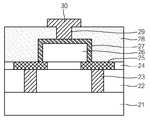
도 3은 본 발명의 실시예에 따른 상변환 기억 소자를 설명하기 위한 단면도.3 is a cross-sectional view illustrating a phase change memory device according to an embodiment of the present invention.
도 4a 내지 도 4d는 본 발명의 실시예에 따른 상변환 기억 소자의 제조방법을 설명하기 위한 공정별 단면도.4A to 4D are cross-sectional views of steps for explaining a method of manufacturing a phase change memory device according to an embodiment of the present invention.
* 도면의 주요 부분에 대한 부호의 설명 *Explanation of symbols on the main parts of the drawings
21 : 반도체 기판22 : 층간절연막21
23 : 하부전극24 : 제1산화막23: lower electrode 24: first oxide film
24a : 트렌치25 : 상변환막24a: trench 25: phase change film
26 : 제2산화막27 : 상부전극26: second oxide film 27: upper electrode
28 : 제3산화막29 : 콘택홀28: third oxide film 29: contact hole
30 : 금속배선30: metal wiring
본 발명은 상변환 기억 소자 및 그 제조방법에 관한 것으로, 보다 상세하게는, 상변환막과 상부전극과의 접촉면적을 줄여 전류량을 감소시킬 수 있는 상변환 기억 소자 및 그 제조방법에 관한 것이다.BACKGROUND OF THE
최근, 전원이 차단되더라도 저장된 데이터가 소멸되지 않는 특징을 갖는 플래쉬 메모리 소자들이 채택되고 있다. 이러한 플래쉬 메로리 소자들은 채널 상에 차례로 적층된 터널산화막, 부유게이트, 게이트 층간 유전체막(Inter-Gate Dielectric Layer) 및 컨트롤 게이트 전극을 포함한다. 따라서, 상기 플래쉬 메모리 소자들의 신뢰성 및 프로그램 효율을 향상시키기 위해서는 터널산화막의 막질이 개선되어야 하고 셀의 커플링 비율이 증가되어야 한다.Recently, flash memory devices having a feature in which stored data are not destroyed even when a power supply is cut off have been adopted. Such flash memory devices include a tunnel oxide film, a floating gate, an inter-gate dielectric layer, and a control gate electrode, which are sequentially stacked on a channel. Therefore, in order to improve the reliability and program efficiency of the flash memory devices, the film quality of the tunnel oxide film should be improved and the coupling ratio of the cell should be increased.
또한, 플래쉬 메모리 소자들 대신에 새로운 비휘발성 메모리 소자들이 최근에 제안되었다. 예를 들면, 상변환 메모리(Phase-Change Memory) 소자들이며, 상변환에 따른 전기저항 차이를 이용하여 정보를 저장하고, 찰코젠나이드(Chalcogenide) 합금재료(Ge2Sb2Te5) 박막이 비정질 상태에서 결정질 상태로 상변환을 하여 결정질 상태일 때 저항 및 활성화 에너지가 낮아지고, 장거리 원자질서와 자유전자 밀도는 높아진다. 상기 상변환 기억 소자의 장점은 Soc(System On Chip)으로 제작하기 쉬우며, 차세대 메모리 반도체 중에서 생산가격이 낮은 편이다. 상기 상변환 기억 소자의 처리속도는 5ns로 매우 빠르며, 소비전력이 낮고 동작온도의 범위는 -196∼180℃로 넓은영역을 가지고 있다.In addition, new nonvolatile memory devices have recently been proposed in place of flash memory devices. For example, these devices are phase-change memory devices, and store information by using electric resistance difference according to a phase change, and the chalcogenide alloy material (Ge2Sb2Te5) thin film is changed from an amorphous state to a crystalline state. Phase transformation results in lower resistance and activation energy when in the crystalline state, and higher long-range atomic order and free electron density. The advantages of the phase change memory device are easy to fabricate with Soc (System On Chip), and low production cost among next generation memory semiconductors. The processing speed of the phase change memory device is very fast, 5ns, low power consumption, and a wide range of operating temperature of -196 to 180 ° C.
도 1은 상변환 메모리 셀을 프로그램 및 소거시키는 방법을 설명하기 위한 도면이다.1 is a diagram for describing a method of programming and erasing a phase change memory cell.
도 1에 도시된 바와 같이, 상기 상변환 박막을 용융온도(Melting Temperature : Tm)보다 높은 온도에서 제 1 동작(First Operation : T1)동안 가열한 후에 냉각시키면, 상기 상변환 박막은 비정질 상태(Amorphous State)로 변한다(A). 반면에, 상기 상변환 박막을 상기 용융온도(Tm)보다 낮고 결정화온도(Crystallization Temperature : Tc)보다 높은 온도에서 상기 제 1 동작(T1)보다 긴 제 2 동작(Second Operation : T2)동안 가열한 후에 냉각시키면, 상기 상변환 물질막은 결정상태(Crystalline State)로 변한다(B). 여기에서, 비정질 상태를 갖는 상변환 박막의 비저항은 결정질 상태를 갖는 상변환 박막의 비저항보다 높다.As shown in FIG. 1, when the phase change thin film is cooled after being heated for a first operation (T1) at a temperature higher than a melting temperature (Tm), the phase change thin film is in an amorphous state. State) (A). On the other hand, after the phase conversion thin film is heated for a second operation longer than the first operation T1 at a temperature lower than the melting temperature Tm and higher than the crystallization temperature Tc, the second operation T2 is performed. Upon cooling, the phase change material film changes to a crystalline state (B). Here, the specific resistance of the phase change thin film having an amorphous state is higher than that of the phase change thin film having a crystalline state.
따라서, 읽기(Read) 모드에서 상기 상변환 박막을 통하여 흐르는 전류를 감지(Detection)함으로써, 상기 상변환 메모리 셀에 저장된 정보가 논리 '1'인지 또는 논리 '0'인지를 판별할 수 있다. 상기 상변환 박막으로는 게르마늄(Ge), 스티비움(Stibium : Sb), 텔루리움(Tellurium : Te)을 함유하는 화합물막(Compound Material Layer; 이하 GST막이라 함)이 널리 사용된다.Accordingly, by detecting the current flowing through the phase change thin film in a read mode, it is possible to determine whether the information stored in the phase change memory cell is logic '1' or logic '0'. As the phase change thin film, a compound film containing a germanium (Ge), stevilium (Sb), and tellurium (Te) (Compound Material Layer; hereinafter referred to as a GST film) is widely used.
도 2는 종래 상변환 메모리 셀을 설명하기 위한 도면이다.2 is a diagram for describing a conventional phase change memory cell.
도 2에 도시된 바와 같이, 종래 상변환 기억 소자는 하부전극(3)을 포함하는 반도체 기판(1) 상에 층간절연막(5)을 형성한다. 그 다음, 상기 층간 절연막(5)을 식각하여 소오스 영역들과 전기적으로 연결되는 콘택플러그(7)를 형성한 후에 콘택플러그(7)를 포함한 기판 결과물 상에 상변환막(9)을 형성한다. 이어서, 상기 상변 환막(9) 상에 상부전극(11)을 형성한다.As shown in FIG. 2, the conventional phase change memory device forms an
상기 상변환 메모리 셀을 프로그램하기 위해 전압을 인가하면, 상기 상변환막(9)과 콘택플러그(7) 사이의 계면에서 열이 발생하여 상변환막의 일부분(9a)이 비정질 상태로 변한다. 상기 상변환막(9)과 콘택플러그(7)의 가장자리(C)의 열은 주변의 층간절연막(7)으로 확산되어 상태변화에 필요한 온도가 되지 않을 수 있다. 이로 인해, 상기 상변환막을 비정질화시킬때 상기 가장자리의 상변환막(9)이 비정질화되지 않은 비정상적 영역이 생성될 수 있다.When a voltage is applied to program the phase change memory cell, heat is generated at the interface between the
또한, 상변화 메모리 소자의 읽기(Read) 및 쓰기(Write) 동작시 상기 상부전극과 상변환막의 접촉면적이 크기 때문에 상변화에 필요한 전류량이 증가하게 되고, 이로 인해 상변환 기억 소자의 속도에도 영향을 주게된다.In addition, since the contact area between the upper electrode and the phase conversion film is large during read and write operations of the phase change memory device, the amount of current required for phase change increases, thereby affecting the speed of the phase change memory device. Will give.
따라서, 본 발명은 상기와 같은 문제점을 해결하기 위해 안출된 것으로서, 상변환막과 상부전극과의 접촉면적을 줄여 전류량을 감소시킬 수 있는 상변환 기억 소자 및 그 제조방법을 제공하는데 그 목적이 있다.Accordingly, an object of the present invention is to provide a phase change memory device and a method of manufacturing the same, which reduce the amount of current by reducing the contact area between the phase change film and the upper electrode. .
상기 목적을 달성하기 위한 본 발명은, 하부패턴이 구비된 반도체 기판; 상기 하부패턴을 덮도록 상기 반도체 기판 상에 형성된 층간절연막; 상기 층간절연막 내에 플러그 형태로 형성된 수 개의 하부전극; 상기 각 하부전극 상에 형성된 상변환막; 상기 상변환막 사이에 형성된 제1산화막; 상기 제1산화막 및 이에 인접한 두 개의 상변환막 부분들 상에 형성된 제2산화막; 상기 제2산화막 상에 형성되며, 이 웃하는 두 개의 상변환막과 동시에 콘택된 상부전극; 상기 단계까지의 기판 결과물 전면 상에 형성된 제3산화막; 상기 제3산화막 내에 상기 상부전극을 노출시키도록 형성된 콘택홀; 및 상기 제3산화막 상에 상기 비아홀을 통해 상기 상부전극과 콘택하도록 형성된 금속배선을 포함하는 것을 특징으로 한다.The present invention for achieving the above object is a semiconductor substrate provided with a lower pattern; An interlayer insulating film formed on the semiconductor substrate to cover the lower pattern; A plurality of lower electrodes formed in a plug shape in the interlayer insulating film; A phase change film formed on each of the lower electrodes; A first oxide film formed between the phase change films; A second oxide film formed on the first oxide film and two phase change film portions adjacent thereto; An upper electrode formed on the second oxide film and simultaneously contacted with two phase change films; A third oxide film formed on the entire surface of the substrate resultant up to this step; A contact hole formed to expose the upper electrode in the third oxide film; And a metal wire formed on the third oxide layer to contact the upper electrode through the via hole.
여기에서, 상기 상부전극은 폴리실리콘막 또는 금속막으로 이루어진 것을 특징으로 한다.Here, the upper electrode is characterized in that made of a polysilicon film or a metal film.
상기 제1산화막은 HDP, USG, SOG, PSG, BPSG, HLD 및 TEOS 산화막으로 구성된 그룹으로부터 선택되는 어느 하나로 이루어진 것을 특징으로 한다.The first oxide film is made of any one selected from the group consisting of HDP, USG, SOG, PSG, BPSG, HLD and TEOS oxide film.
또한, 본 발명은 하부패턴이 구비된 반도체 기판을 제공하는 단계; 상기 반도체 기판 상에 상기 하부패턴을 덮도록 층간절연막을 형성하는 단계; 상기 층간절연막 내에 플러그 형태로 수 개의 하부전극을 형성하는 단계; 상기 하부전극을 포함한 층간절연막 상에 제1산화막을 형성하는 단계; 상기 각 하부전극을 노출시키는 트렌치가 형성되도록 상기 제1산화막을 패터닝하는 단계; 상기 노출된 하부전극과 콘택하도록 상기 트렌치 내에 상변환막을 매립시키는 단계; 상기 상변환막을 포함한 제1산화막 상에 제2산화막을 형성하는 단계; 상기 상변환막 사이의 제1산화막 및 이에 인접한 두 개의 상변환막 부분 상에 잔류되도록 상기 제2산화막을 패터닝하는 단계; 상기 패터닝된 제2산화막과 상변환막 및 제1산화막 상에 도전막을 형성하는 단계; 상기 도전막을 패터닝하여 상기 패터닝된 제2산화막을 둘러싸면서 이웃하는 두 개의 상변환막과 동시에 콘택하는 상부전극을 형성하는 단계; 상기 단계까지의 기판 결과물 상에 제3산화막을 형성하는 단계; 상기 제3산화막을 식각하여 상 기 상부전극을 노출시키는 콘택홀을 형성하는 단계; 및 상기 제3산화막 상에 상기 노출된 상부전극과 콘택되는 금속배선을 형성하는 단계를 포함하는 것을 특징으로 한다.In addition, the present invention comprises the steps of providing a semiconductor substrate having a lower pattern; Forming an interlayer insulating film on the semiconductor substrate to cover the lower pattern; Forming several lower electrodes in the form of a plug in the interlayer insulating film; Forming a first oxide film on the interlayer insulating film including the lower electrode; Patterning the first oxide film to form trenches for exposing the lower electrodes; Embedding a phase change layer in the trench to contact the exposed lower electrode; Forming a second oxide film on the first oxide film including the phase conversion film; Patterning the second oxide film so as to remain on the first oxide film between the phase change film and two portions of the phase change film adjacent thereto; Forming a conductive film on the patterned second oxide film, the phase change film, and the first oxide film; Patterning the conductive layer to form an upper electrode surrounding the patterned second oxide layer and simultaneously contacting two adjacent phase change layers; Forming a third oxide film on the substrate resultant up to this step; Etching the third oxide layer to form a contact hole exposing the upper electrode; And forming a metal wiring on the third oxide layer, the metal wiring being in contact with the exposed upper electrode.
여기에서, 상기 제1산화막은 HDP, USG, SOG, PSG, BPSG, HDL 및 TEOS 산화막으로 구성되는 그룹으로부터 선택되는 어느 하나로 형성하는 것을 특징으로 한다.Here, the first oxide film is formed of any one selected from the group consisting of HDP, USG, SOG, PSG, BPSG, HDL, and TEOS oxide film.
상기 트렌치 내에 상변환막을 매립시키는 단계는 상기 트렌치 및 제1산화막 상에 상변환막을 형성하는 단계; 및 상기 제1산화막이 노출되도록 상기 상변환막을 CMP하는 단계로 구성되는 것을 특징으로 한다.The step of embedding a phase change film in the trench may include forming a phase change film on the trench and the first oxide film; And CMPing the phase change film to expose the first oxide film.
상기 상부전극은 폴리실리콘막 또는 금속막으로 형성하는 것을 특징으로 한다.The upper electrode may be formed of a polysilicon film or a metal film.
상기 상부전극은 그 형성 두께에 따라 상기 상변환막과의 접촉 면적이 결정되는 것을 특징으로 한다.The upper electrode is characterized in that the contact area with the phase change film is determined according to the thickness of the upper electrode.
(실시예)(Example)
이하, 본 발명의 바람직한 실시예에 대해 첨부된 도면을 참조하여 상세하게 설명한다.Hereinafter, exemplary embodiments of the present invention will be described in detail with reference to the accompanying drawings.
도 3은 본 발명의 실시예에 따른 상변환 기억 소자를 설명하기 위한 단면도이다.3 is a cross-sectional view illustrating a phase change memory device according to an embodiment of the present invention.
도 3에 도시된 바와 같이, 본 발명의 상변환 기억 소자는 하부패턴(미도시)이 구비된 반도체 기판(21) 상에 하부패턴을 덮도록 층간절연막(22)이 형성된다. 여기서, 상기 하부패턴은 일반적인 상변화 기억 소자에 구비되는 패턴으로서, 스위칭 소자, 예를 들어, 트랜지스터, 또는, 다이오드로 이루어진 스위칭 소자를 포함한다. 상기 층간절연막(22) 내에 플러그 형태로 형성된 하부전극(23)을 형성하고, 상기 각 하부전극(23)을 포함한 층간절연막(22) 상에 제1산화막(24)이 형성된다. 상기 각 하부전극(23) 상에 상변환막(25)이 형성되고, 상기 제1산화막(24) 및 이에 인접한 두 개의 상변환막(25) 부분들 상에 제2산화막(26)이 형성된다. 상기 제2산화막(26) 상에 형성되며, 이웃하는 두 개의 상변환막(25)과 동시에 콘택되는 상부전극(27)이 형성된다. 상기 상부전극(27)을 포함한 기판 결과물 전면 상에 제3산화막(28)이 형성되고, 상기 제3산화막(28) 내에 상기 상부전극(27)을 노출시키는 콘택홀(29)이 형성된다. 상기 제3산화막(28) 상에 상기 콘택홀(29)을 통해 상기 상부전극(27)과 콘택하도록 금속배선(30)을 형성한다.As shown in FIG. 3, in the phase change memory device of the present invention, an interlayer
상기 제1산화막(24)은 HDP, USG, SOG, PSG, BPSG, HDL 및 TEOS 산화막으로 구성되는 그룹으로부터 선택되는 어느 하나로 이루어지는 것이 바람직하다. 상기 상부전극(27)은 폴리실리콘막 및 금속막으로 형성하는 것이 바람직하다.The
상기 상변화 메모리 소자의 읽기(Read) 및 쓰기(Write) 동작시 상기 상변환막(25)의 접촉면에서 열이 발생하면, 상기 상변환막의 상태가 비정질 상태 또는 결정질 상태로 변한다. 본 발명의 상변환 기억 소자는 상부전극(27)이 이웃하는 두 개의 상변환막(25)과 동시에 콘택하도록 형성되어 있어 상변환막(25)과 상부전극(27)의 접촉면적(D)이 작기 때문에 상변화에 필요한 전류를 감소시킬 수 있으므로, 상변환 기억 소자의 속도를 향상시킬 수 있다. 즉, 본 발명에서는 상기 상부전극(27)이 이웃하는 두 개의 상변환막(25) 사이의 제2산화막(26) 상에 형성되어, 상기 제2산화막(26)을 사이에 두고 이웃하는 두 개의 상변환막(25)의 일 부분과 동시에 콘택하고 있어서, 상기 상부전극(27)이 하나의 상변환막(25)과 각각 전체적으로 콘택하는 경우에 비해, 상대적으로 작은 접촉면적을 갖는다.When heat is generated at the contact surface of the
도 4a 내지 도 4d는 본 발명의 실시예에 따른 상변환 기억 소자의 제조방법을 설명하기 위한 공정별 단면도이다.4A through 4D are cross-sectional views illustrating processes of manufacturing a phase change memory device according to an exemplary embodiment of the present invention.
도 4a에 도시된 바와 같이, 하부패턴(미도시)을 포함하는 반도체 기판(21) 상에 하부패턴을 덮도록 층간절연막(22)을 형성한다. 여기서, 상기 하부패턴은 일반적인 상변화 기억 소자에 구비되는 패턴으로서, 스위칭 소자, 예를 들어, 트랜지스터, 또는, 다이오드로 이루어진 스위칭 소자를 포함한다. 그 다음, 상기 층간절연막(22)을 식각하여 하부전극(23)을 플러그 형태로 형성한 후에 상기 하부전극(23)을 포함한 층간절연막(22) 상에 제1산화막(24)을 형성한다. 이때, 제1산화막(24)은 HDP, USG, SOG, PSG, BPSG, HDL 및 TEOS 산화막으로 구성되는 그룹으로부터 선택된 어느 하나로 이루어지는 것이 바람직하다. 이어서, 상기 각 하부전극(23)을 노출시키는 트렌치(24a)가 형성되도록 상기 제1산화막(24)을 패터닝한다.As shown in FIG. 4A, the
도 4b에 도시된 바와 같이, 상기 노출된 하부전극(23)과 콘택하도록 상기 트렌치(24a) 및 제1산화막(24) 상에 상변환막(25)을 매립한다. 그 다음, 상기 제1산화막(24)이 노출되도록 상변환막(25)을 CMP한다.As shown in FIG. 4B, a
도 4c에 도시된 바와 같이, 상기 상변환막(25)을 포함한 제1산화막(24) 상에 제2산화막(26)을 형성한다. 이어서, 상기 상변환막(25) 사이의 제1산화막(24) 및 이에 인접한 두 개의 상변환막(25) 부분 상에 잔류되도록 상기 제2산화막(26)을 패터닝한다. 그 다음, 상기 패터닝된 제2산화막(26)과 상변환막(25) 및 제1산화막 (24) 상에 도전막을 형성한다. 이어서, 상기 도전막을 패터닝하여 상기 패터닝된 제2산화막(26)을 둘러싸면서 이웃하는 두 개의 상변환막과 동시에 콘택하는 상부전극(27)을 형성한다. 이때, 상기 상부전극(27)은 폴리실리콘막 또는 금속막으로 형성하며, 상기 상부전극(27) 형성 두께에 따라 상변환막(25)과의 접촉 면적이 결정된다.As shown in FIG. 4C, a
도 4d에 도시된 바와 같이, 상기 상부전극(27)을 포함한 기판 결과물 상에 제3산화막(28)을 형성한다. 그 다음, 상기 제3산화막(28)을 식각하여 상기 상부전극(27)을 노출시키는 콘택홀(29)을 형성한다. 이어서, 상기 제3산화막(28) 상에 노출된 상부전극(27)과 콘택되는 금속배선(30)을 형성한다. 여기에서, 제2산화막(26) 및 제3산화막(28)은 제1산화막(24)과 동일하게 형성하거나 또는 다르게 형성할 수 있다.As shown in FIG. 4D, a
전술한 바와 같이, 본 발명은 상변환 기억 소자 제조시 상부전극(27)이 이웃하는 두 개의 상변환막(25)과 동시에 콘택하도록 형성되어 있어 상부전극(27)과 상변환막(25)의 접촉면적을 줄임으로써 상변화에 필요한 전류량을 감소시킬 수 있으며, 이로 인해 상변환 기억 소자의 속도를 향상시킬 수 있다. 즉, 본 발명에서는 상기 상부전극(27)이 이웃하는 두 개의 상변환막(25) 사이의 제2산화막(26) 상에 형성되어, 상기 제2산화막(26)을 사이에 두고 이웃하는 두 개의 상변환막(25)의 일 부분과 동시에 콘택하고 있어서, 상기 상부전극(27)이 하나의 상변환막(25)과 각각 전체적으로 콘택하는 경우에 비해, 상대적으로 작은 접촉면적을 가질 수 있는 것이다.As described above, in the manufacturing of the phase change memory device, the
이상, 본 발명을 몇 가지 예를 들어 설명하였으나, 본 발명은 이에 한정되는 것은 아니며, 본 발명이 속하는 기술분야에서 통상의 지식을 가진 자라면 본 발명의 사상에서 벗어나지 않으면서 많은 수정과 변형을 가할 수 있음을 이해할 것이다.In the above, the present invention has been described with reference to some examples, but the present invention is not limited thereto, and a person of ordinary skill in the art may make many modifications and variations without departing from the spirit of the present invention. I will understand.
이상에서와 같이, 본 발명은 상변환막의 상변화가 용이하게 일어나도록 하기 위해 상부전극이 이웃하는 두 개의 상변환막과 동시에 콘택하도록 형성되어 있어 상부전극과 상변환막의 접촉면적을 줄임으로써 상변화에 필요한 전류량을 감소시킬 수 있다. 즉, 본 발명에서는 상기 상부전극이 이웃하는 두 개의 상변환막 사이의 제2산화막 상에 형성되어, 상기 제2산화막을 사이에 두고 이웃하는 두 개의 상변환막의 일 부분과 동시에 콘택하고 있어서, 상기 상부전극이 하나의 상변환막과 각각 전체적으로 콘택하는 경우에 비해, 상대적으로 작은 접촉면적을 갖는다.As described above, in order to facilitate the phase change of the phase change film, the present invention is formed such that the upper electrode contacts the two adjacent phase change films at the same time, thereby reducing the contact area between the upper electrode and the phase change film. Can reduce the amount of current required. That is, in the present invention, the upper electrode is formed on a second oxide film between two adjacent phase change films, and simultaneously contacts a portion of two adjacent phase change films with the second oxide film interposed therebetween. Compared to the case where the upper electrode contacts the one phase conversion film as a whole, it has a relatively small contact area.
따라서, 상변환에 필요한 전류량을 감소시킴으로써 상변환 기억 소자의 속도를 향상시킬 수 있다.Therefore, the speed of the phase conversion memory element can be improved by reducing the amount of current required for phase conversion.
Claims (8)
Translated fromKoreanPriority Applications (1)
| Application Number | Priority Date | Filing Date | Title |
|---|---|---|---|
| KR1020040050075AKR101052861B1 (en) | 2004-06-30 | 2004-06-30 | Phase change memory device and its manufacturing method |
Applications Claiming Priority (1)
| Application Number | Priority Date | Filing Date | Title |
|---|---|---|---|
| KR1020040050075AKR101052861B1 (en) | 2004-06-30 | 2004-06-30 | Phase change memory device and its manufacturing method |
Publications (2)
| Publication Number | Publication Date |
|---|---|
| KR20060001058A KR20060001058A (en) | 2006-01-06 |
| KR101052861B1true KR101052861B1 (en) | 2011-07-29 |
Family
ID=37104255
Family Applications (1)
| Application Number | Title | Priority Date | Filing Date |
|---|---|---|---|
| KR1020040050075AExpired - Fee RelatedKR101052861B1 (en) | 2004-06-30 | 2004-06-30 | Phase change memory device and its manufacturing method |
Country Status (1)
| Country | Link |
|---|---|
| KR (1) | KR101052861B1 (en) |
Families Citing this family (2)
| Publication number | Priority date | Publication date | Assignee | Title |
|---|---|---|---|---|
| KR100679270B1 (en)* | 2006-01-27 | 2007-02-06 | 삼성전자주식회사 | Phase change memory device and manufacturing method thereof |
| US7560723B2 (en)* | 2006-08-29 | 2009-07-14 | Micron Technology, Inc. | Enhanced memory density resistance variable memory cells, arrays, devices and systems including the same, and methods of fabrication |
Citations (2)
| Publication number | Priority date | Publication date | Assignee | Title |
|---|---|---|---|---|
| JP2003151182A (en) | 2001-11-15 | 2003-05-23 | Dainippon Printing Co Ltd | Method of manufacturing phase change memory device and memory device manufactured by the method |
| JP2003317466A (en) | 2002-04-17 | 2003-11-07 | Sony Corp | Storage device using resistance change storage element and method for determining reference resistance value of the device |
- 2004
- 2004-06-30KRKR1020040050075Apatent/KR101052861B1/ennot_activeExpired - Fee Related
Patent Citations (2)
| Publication number | Priority date | Publication date | Assignee | Title |
|---|---|---|---|---|
| JP2003151182A (en) | 2001-11-15 | 2003-05-23 | Dainippon Printing Co Ltd | Method of manufacturing phase change memory device and memory device manufactured by the method |
| JP2003317466A (en) | 2002-04-17 | 2003-11-07 | Sony Corp | Storage device using resistance change storage element and method for determining reference resistance value of the device |
Also Published As
| Publication number | Publication date |
|---|---|
| KR20060001058A (en) | 2006-01-06 |
Similar Documents
| Publication | Publication Date | Title |
|---|---|---|
| KR100639206B1 (en) | Phase change memory device and its manufacturing method | |
| KR100668823B1 (en) | Phase change memory device and its manufacturing method | |
| KR100568109B1 (en) | Phase change memory device and its formation method | |
| US8686393B2 (en) | Integrated circuit semiconductor devices including channel trenches and related methods of manufacturing | |
| JP2004158852A (en) | Phase change storage element and method of manufacturing the same | |
| KR100650761B1 (en) | Phase change memory device and manufacturing method thereof | |
| KR101052860B1 (en) | Phase change memory device and its manufacturing method | |
| KR101052861B1 (en) | Phase change memory device and its manufacturing method | |
| JP4955218B2 (en) | Semiconductor device | |
| KR100650718B1 (en) | Phase change memory device and its manufacturing method | |
| KR100650719B1 (en) | Phase change memory device and its manufacturing method | |
| US20070241385A1 (en) | Phase change memory device for optimized current consumption efficiency and operation speed and method of manufacturing the same | |
| KR100997785B1 (en) | Phase change memory device and its manufacturing method | |
| KR101052862B1 (en) | Phase change memory device and its manufacturing method | |
| KR101052859B1 (en) | Phase change memory device and its manufacturing method | |
| KR20060001049A (en) | Phase change memory device and its manufacturing method | |
| KR20060001050A (en) | Manufacturing method of phase change memory device | |
| KR101178835B1 (en) | Method of manufacturing phase change RAM device | |
| KR100650720B1 (en) | Phase change memory device and manufacturing method thereof | |
| KR20060001088A (en) | Phase change memory device and its manufacturing method | |
| KR100668870B1 (en) | Phase change memory device and manufacturing method thereof | |
| KR20060001101A (en) | Phase change memory device and manufacturing method thereof | |
| KR20070036940A (en) | Phase change memory device and manufacturing method thereof | |
| KR20060001090A (en) | Phase change memory device and its manufacturing method | |
| KR20060001087A (en) | Phase change memory device and its manufacturing method |
Legal Events
| Date | Code | Title | Description |
|---|---|---|---|
| PA0109 | Patent application | St.27 status event code:A-0-1-A10-A12-nap-PA0109 | |
| PG1501 | Laying open of application | St.27 status event code:A-1-1-Q10-Q12-nap-PG1501 | |
| A201 | Request for examination | ||
| PA0201 | Request for examination | St.27 status event code:A-1-2-D10-D11-exm-PA0201 | |
| E902 | Notification of reason for refusal | ||
| PE0902 | Notice of grounds for rejection | St.27 status event code:A-1-2-D10-D21-exm-PE0902 | |
| P11-X000 | Amendment of application requested | St.27 status event code:A-2-2-P10-P11-nap-X000 | |
| P13-X000 | Application amended | St.27 status event code:A-2-2-P10-P13-nap-X000 | |
| E701 | Decision to grant or registration of patent right | ||
| PE0701 | Decision of registration | St.27 status event code:A-1-2-D10-D22-exm-PE0701 | |
| GRNT | Written decision to grant | ||
| PR0701 | Registration of establishment | St.27 status event code:A-2-4-F10-F11-exm-PR0701 | |
| PR1002 | Payment of registration fee | St.27 status event code:A-2-2-U10-U11-oth-PR1002 Fee payment year number:1 | |
| PG1601 | Publication of registration | St.27 status event code:A-4-4-Q10-Q13-nap-PG1601 | |
| PN2301 | Change of applicant | St.27 status event code:A-5-5-R10-R13-asn-PN2301 St.27 status event code:A-5-5-R10-R11-asn-PN2301 | |
| PN2301 | Change of applicant | St.27 status event code:A-5-5-R10-R13-asn-PN2301 St.27 status event code:A-5-5-R10-R11-asn-PN2301 | |
| LAPS | Lapse due to unpaid annual fee | ||
| PC1903 | Unpaid annual fee | St.27 status event code:A-4-4-U10-U13-oth-PC1903 Not in force date:20140726 Payment event data comment text:Termination Category : DEFAULT_OF_REGISTRATION_FEE | |
| PN2301 | Change of applicant | St.27 status event code:A-5-5-R10-R13-asn-PN2301 St.27 status event code:A-5-5-R10-R11-asn-PN2301 | |
| PC1903 | Unpaid annual fee | St.27 status event code:N-4-6-H10-H13-oth-PC1903 Ip right cessation event data comment text:Termination Category : DEFAULT_OF_REGISTRATION_FEE Not in force date:20140726 | |
| P22-X000 | Classification modified | St.27 status event code:A-4-4-P10-P22-nap-X000 | |
| P22-X000 | Classification modified | St.27 status event code:A-4-4-P10-P22-nap-X000 |