KR101051004B1 - An array substrate for LCD with type TFT and method of fabrication thereof - Google Patents
An array substrate for LCD with type TFT and method of fabrication thereofDownload PDFInfo
- Publication number
- KR101051004B1 KR101051004B1KR1020040099753AKR20040099753AKR101051004B1KR 101051004 B1KR101051004 B1KR 101051004B1KR 1020040099753 AKR1020040099753 AKR 1020040099753AKR 20040099753 AKR20040099753 AKR 20040099753AKR 101051004 B1KR101051004 B1KR 101051004B1
- Authority
- KR
- South Korea
- Prior art keywords
- layer
- amorphous silicon
- silicon layer
- forming
- driving element
- Prior art date
- Legal status (The legal status is an assumption and is not a legal conclusion. Google has not performed a legal analysis and makes no representation as to the accuracy of the status listed.)
- Expired - Fee Related
Links
Images


Classifications
- H—ELECTRICITY
- H10—SEMICONDUCTOR DEVICES; ELECTRIC SOLID-STATE DEVICES NOT OTHERWISE PROVIDED FOR
- H10D—INORGANIC ELECTRIC SEMICONDUCTOR DEVICES
- H10D86/00—Integrated devices formed in or on insulating or conducting substrates, e.g. formed in silicon-on-insulator [SOI] substrates or on stainless steel or glass substrates
- H10D86/40—Integrated devices formed in or on insulating or conducting substrates, e.g. formed in silicon-on-insulator [SOI] substrates or on stainless steel or glass substrates characterised by multiple TFTs
- H10D86/421—Integrated devices formed in or on insulating or conducting substrates, e.g. formed in silicon-on-insulator [SOI] substrates or on stainless steel or glass substrates characterised by multiple TFTs having a particular composition, shape or crystalline structure of the active layer
- H10D86/425—Integrated devices formed in or on insulating or conducting substrates, e.g. formed in silicon-on-insulator [SOI] substrates or on stainless steel or glass substrates characterised by multiple TFTs having a particular composition, shape or crystalline structure of the active layer having different crystal properties in different TFTs or within an individual TFT
- G—PHYSICS
- G02—OPTICS
- G02F—OPTICAL DEVICES OR ARRANGEMENTS FOR THE CONTROL OF LIGHT BY MODIFICATION OF THE OPTICAL PROPERTIES OF THE MEDIA OF THE ELEMENTS INVOLVED THEREIN; NON-LINEAR OPTICS; FREQUENCY-CHANGING OF LIGHT; OPTICAL LOGIC ELEMENTS; OPTICAL ANALOGUE/DIGITAL CONVERTERS
- G02F1/00—Devices or arrangements for the control of the intensity, colour, phase, polarisation or direction of light arriving from an independent light source, e.g. switching, gating or modulating; Non-linear optics
- G02F1/01—Devices or arrangements for the control of the intensity, colour, phase, polarisation or direction of light arriving from an independent light source, e.g. switching, gating or modulating; Non-linear optics for the control of the intensity, phase, polarisation or colour
- G02F1/13—Devices or arrangements for the control of the intensity, colour, phase, polarisation or direction of light arriving from an independent light source, e.g. switching, gating or modulating; Non-linear optics for the control of the intensity, phase, polarisation or colour based on liquid crystals, e.g. single liquid crystal display cells
- G02F1/133—Constructional arrangements; Operation of liquid crystal cells; Circuit arrangements
- G02F1/136—Liquid crystal cells structurally associated with a semi-conducting layer or substrate, e.g. cells forming part of an integrated circuit
- G02F1/1362—Active matrix addressed cells
- G02F1/1368—Active matrix addressed cells in which the switching element is a three-electrode device
- H—ELECTRICITY
- H10—SEMICONDUCTOR DEVICES; ELECTRIC SOLID-STATE DEVICES NOT OTHERWISE PROVIDED FOR
- H10D—INORGANIC ELECTRIC SEMICONDUCTOR DEVICES
- H10D86/00—Integrated devices formed in or on insulating or conducting substrates, e.g. formed in silicon-on-insulator [SOI] substrates or on stainless steel or glass substrates
- H10D86/01—Manufacture or treatment
- H10D86/021—Manufacture or treatment of multiple TFTs
- H10D86/0231—Manufacture or treatment of multiple TFTs using masks, e.g. half-tone masks
- H—ELECTRICITY
- H10—SEMICONDUCTOR DEVICES; ELECTRIC SOLID-STATE DEVICES NOT OTHERWISE PROVIDED FOR
- H10D—INORGANIC ELECTRIC SEMICONDUCTOR DEVICES
- H10D86/00—Integrated devices formed in or on insulating or conducting substrates, e.g. formed in silicon-on-insulator [SOI] substrates or on stainless steel or glass substrates
- H10D86/40—Integrated devices formed in or on insulating or conducting substrates, e.g. formed in silicon-on-insulator [SOI] substrates or on stainless steel or glass substrates characterised by multiple TFTs
- H10D86/441—Interconnections, e.g. scanning lines
Landscapes
- Physics & Mathematics (AREA)
- Nonlinear Science (AREA)
- Engineering & Computer Science (AREA)
- Microelectronics & Electronic Packaging (AREA)
- Mathematical Physics (AREA)
- Chemical & Material Sciences (AREA)
- Crystallography & Structural Chemistry (AREA)
- General Physics & Mathematics (AREA)
- Optics & Photonics (AREA)
- Thin Film Transistor (AREA)
- Liquid Crystal (AREA)
Abstract
Translated fromKoreanDescription
Translated fromKorean도 1은 일반적인 액정패널의 개략적인 도면.1 is a schematic view of a general liquid crystal panel.
도 2는 종래의 제1 예에 따른 구동회로 일체형 액정표시장치용 어레이기판의 비정질실리콘 박막트랜지스터 제조공정을 나타낸 블록도.2 is a block diagram illustrating an amorphous silicon thin film transistor fabrication process of an array substrate for a liquid crystal display device with a driving circuit integrated according to a first example of the related art.
도 3은 종래의 제1 예에 따른 구동회로 일체형 액정표시장치용 어레이기판의 비정질실리콘 박막트랜지스터의 단면도.3 is a cross-sectional view of an amorphous silicon thin film transistor of an array substrate for a liquid crystal display device integrated with a driving circuit according to a first conventional example.
도 4는 종래의 제2 예에 따른 구동회로 일체형 폴리실리콘 박막트랜지스터 제조공정을 나타낸 블록도.4 is a block diagram illustrating a process of manufacturing a polysilicon thin film transistor integrated with a driving circuit according to a second conventional example.
도 5는 종래의 제2 예에 따른 구동회로 일체형 액정표시장치용 어레이기판의 폴리실리콘 박막트랜지스터의 단면도.5 is a cross-sectional view of a polysilicon thin film transistor of an array substrate for a drive circuit-integrated liquid crystal display device according to a second conventional example.
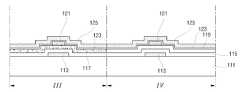
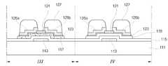
도 6a ~ 도 6k는 본 발명의 실시 예에 따른 구동소자부에 폴리실리콘 박막트랜지스터를 포함하고, 표시부에 비정질실리콘 박막트랜지스터를 포함하는 구동회로 일체형 액정표시장치용 어레이기판의 제조방법을 공정순서에 따라 개략적으로 도시한 단면도.6A to 6K illustrate a method of manufacturing an array substrate for a liquid crystal display device with a driving circuit incorporating a polysilicon thin film transistor in a driving element portion and an amorphous silicon thin film transistor in a display portion, according to an embodiment of the present invention. Schematically shown in cross section.
<도면의 주요부분에 대한 부호의 설명><Description of the symbols for the main parts of the drawings>
111: 기판113: 게이트전극111
115: 게이트절연막117: 다결정실리콘층115: gate insulating film 117: polysilicon layer
119: 비정질실리콘층121: 에치스토퍼층119: amorphous silicon layer 121: etch stopper layer
123: 불순물비정질층126a: 소스전극123: impurity
126b: 드레인전극129: 보호층126b: drain electrode 129: protective layer
133: 화소전극
133: pixel electrode
본 발명은 액정표시장치에 관한 것으로 특히, 구동소자로 다결정 박막트랜지스터를 사용하고 스위칭소자로 비정질 박막트랜지스터를 사용한 액정표시장치용 어레이기판 및 그 제조방법에 관한 것이다.The present invention relates to a liquid crystal display device, and more particularly, to an array substrate for a liquid crystal display device using a polycrystalline thin film transistor as a driving element and an amorphous thin film transistor as a switching element, and a manufacturing method thereof.
일반적인 액정표시장치는 전계를 이용하여 액정의 광투과율을 조절함으로써 화상을 표시하게 된다. 이를 위하여 액정표시장치는 액정셀들이 매트릭스 형태로 배열되어진 액정패널과 액정패널을 구동하기 위한 구동회로를 구비한다.A general liquid crystal display device displays an image by adjusting a light transmittance of a liquid crystal using an electric field. To this end, the liquid crystal display includes a liquid crystal panel in which liquid crystal cells are arranged in a matrix and a driving circuit for driving the liquid crystal panel.
액정표시패널에는 다수의 화소를 구성하며, 각 화소의 일측과 타측을 따라 게이트라인들과 데이터라인들이 교차하게 배열되고 상기 각 화소에 액정셀들이 위치하게 된다. 이 액정표시패널에는 액정셀들 각각에 전계를 인가하기 위한 화소전 극들과 공통전극이 마련된다.A plurality of pixels are configured in the liquid crystal display panel, and gate lines and data lines are arranged to cross each other along one side and the other side of each pixel, and liquid crystal cells are positioned in each pixel. The liquid crystal display panel is provided with pixel electrodes and a common electrode for applying an electric field to each of the liquid crystal cells.
도 1은 일반적인 구동회로 일체형 액정표시장치의 개략적인 평면도이다.1 is a schematic plan view of a general liquid crystal display device integrated with a driving circuit.
화소전극(PE)들 각각은 스위칭소자인 박막트랜지스터(T)의 소스 및 드레인 단자들을 경유하여 데이터라인(DL)에 접속된다. 구동소자부(GP, DP)는 게이트라인(GL)들을 구동하기 위한 게이트구동회로(GP)와 데이터라인(DL)들을 구동하기 위한 데이터구동회로(DP)를 구비한다.Each of the pixel electrodes PE is connected to the data line DL via source and drain terminals of the thin film transistor T, which is a switching element. The driving element units GP and DP include a gate driving circuit GP for driving the gate lines GL and a data driving circuit DP for driving the data lines DL.
게이트구동회로(GP)는 스캐닝신호를 게이트라인(GL)들에 순차적으로 공급하여 액정표시패널 상의 액정셀들을 순차적으로 구동한다.The gate driving circuit GP sequentially supplies the scanning signals to the gate lines GL to sequentially drive the liquid crystal cells on the liquid crystal display panel.
데이터구동회로(DP)는 게이트라인(GL)들 중 어느 하나에 게이트신호가 공급될 때마다 데이터라인(DL)들 각각에 비디오신호를 공급한다. 이러한 비디오신호에 따라 화소전극(P)과 공통전극사이에 인가되는 전계에 의해 액정셀의 광투과율을 조절함으로써 표시부(4)로 화상을 표시하게 된다.The data driver circuit DP supplies a video signal to each of the data lines DL whenever the gate signal is supplied to any one of the gate lines GL. According to the video signal, an image is displayed on the
이러한 액정표시장치에 이용되는 박막트랜지스터(T)는 액티브층으로 비정질실리콘(a-si:H) 또는 폴리실리콘(p-si:H)을 이용한다.The thin film transistor T used in such a liquid crystal display uses amorphous silicon (a-si: H) or polysilicon (p-si: H) as an active layer.
일반적으로, 상기 액티브층을 비정질실리콘으로 사용할 경우에는 게이트전극이 하부에 구성된 인버티드 스테거드 타입(Inverted staggered type)으로 박막트랜지스터를 사용하게 되며, 상기 인버티드 스테거드 타입 또한 에치백 타입(etch-back type)과 에치스토퍼 타입(etch-stopper type)으로 나눌 수 있다.In general, when the active layer is used as amorphous silicon, a thin film transistor is used as an inverted staggered type having a gate electrode formed at a lower portion thereof, and the inverted staggered type is also an etch-back type. back type) and etch-stopper type.
에치백 타입은 비정질실리콘층이 과식각되므로 비정질실리콘층이 두꺼워야 하는데, 비정질실리콘층이 두꺼울수록 빛에 대한 민감도 증가로 누설전류가 많아지 는 단점이 있다.In the etchback type, the amorphous silicon layer is overetched, so the amorphous silicon layer should be thick. However, the thicker the amorphous silicon layer, the more the leakage current increases due to the increased sensitivity to light.
에치스토퍼 타입은 에치백 타입과는 다르게 채널부의 에치스토퍼층이 비정질실리콘층의 식각을 방지하여 비정질실리콘층의 두께를 얇게 형성할 수 있는 장점이 있다.Unlike the etch back type, the etch stopper type has an advantage that the etch stopper layer of the channel portion prevents the etching of the amorphous silicon layer to form a thin thickness of the amorphous silicon layer.
이하, 도면을 참조하여 일반적인 에치스토퍼 타입의 박막트랜지스터를 포함하는 구동회로 일체형 액정표시장치용 어레이기판의 제조공정을 설명한다.Hereinafter, a manufacturing process of an array substrate for a liquid crystal display device including a driving circuit including a thin film transistor of a general etch stopper type will be described with reference to the drawings.
도 2는 일반적으로 적용되는 구동회로일체형 액정표시장치용 어레이기판의 비정질실리콘 박막트랜지스터의 제작 공정을 도시한 흐름도로써, 도 3의 구동회로 일체형 액정표시장치용 어레이기판의 비정질실리콘 박막트랜지스터의 단면도를 참조하여 설명한다.FIG. 2 is a flowchart illustrating a manufacturing process of an amorphous silicon thin film transistor of an array substrate for a driving circuit integrated liquid crystal display device, which is generally applied, and a cross-sectional view of an amorphous silicon thin film transistor of the array substrate for a driving circuit integrated liquid crystal display device of FIG. 3. It demonstrates with reference.
제1단계(st1)는 제 1마스크공정으로, 구동소자부(Ⅰ)와 표시부(Ⅱ)가 정의된 투명한 절연기판(3) 상에 게이트전극(5)을 형성한다. 상기 게이트전극(5)을 형성한 기판(3)의 전면에 질화실리콘(SiNx)과 산화실리콘(SiO2)을 포함한 무기절연 물질 그룹 중 선택된 하나를 증착하여 제1절연막인 게이트절연막(7)을 형성한다.The first step st1 is a first mask process, in which the
제2단계(st2)는 제2마스크공정으로, 상기 게이트절연막(7) 상부에 순수 비정질실리콘층(미도시)을 형성한다. 상기 순수 비정질실리콘층(미도시)의 상부에 질화실리콘(SiNx)과 산화실리콘(SiO2)을 포함하는 무기절연물질 그룹 중 선택된 하나를 증착하고 패터닝하여 에치스토퍼층(11)을 형성한다.The second step st2 is a second mask process to form a pure amorphous silicon layer (not shown) on the
다음은 제3단계(st3)의 제3마스크공정으로, 상기 에치스토퍼층(11)이 형성된 기판(3)의 전면에 불순물 비정질실리콘층(미도시)을 적층한다.Next, in the third mask process of the third step (st3), an impurity amorphous silicon layer (not shown) is laminated on the entire surface of the
동시에, 상기 불순물 비정질실리콘층(미도시) 상부에 금속층(미도시)을 적층하여 형성한다.At the same time, a metal layer (not shown) is formed on the impurity amorphous silicon layer (not shown).
상기 적층된 금속층과 그 하부의 불순물 비정질실리콘층과, 부분적으로 결정화된 순수 비정질실리콘층을 회절노광법을 이용한 마스크공정으로 패터닝하여, 상기 소스 및 드레인영역에 서로 이격되도록 소스전극(15a)과 드레인전극(15b)을 형성한다.The stacked metal layer, an impurity amorphous silicon layer below it, and a partially crystallized pure amorphous silicon layer are patterned by a mask process using a diffraction exposure method, so that the
연속하여, 상기 이격된 소스 및 드레인전극(15a, 15b)의 하부에 이와 접촉하는 오믹콘택층(13)과 , 오믹콘택층(13)의 하부에 액티브층(9)을 형성한다.Subsequently, an
제4단계(st4)는 제4마스크공정으로, 상기 소스 및 드레인전극(15a, 15b)이 형성된 기판(3)의 전면에 제2절연막인 보호층(17)을 형성한다. 연속하여 상기 표시부(Ⅱ)의 보호층(17)을 패터닝하여 상기 드레인전극(15b)의 일부를 노출하는 콘택홀(미도시)을 형성한다.The fourth step st4 is a fourth mask process to form the
제5단계(st5)는 제5마스크공정으로, 상기 표시부(Ⅱ)의 보호층(17)이 형성된 기판(3)의 전면에 인듐-틴 옥사이드(ITO)와 인듐-징크-옥사이드(IZO)를 포함하는 투명 도전성 금속물질 그룹 중 선택된 하나를 증착하고 제5마스크 공정으로 패터닝하여, 상기 드레인전극(15b)과 접촉하는 투명 화소전극(19)을 형성한다.The fifth step (st5) is a fifth mask process in which indium tin oxide (ITO) and indium zinc oxide (IZO) are applied to the entire surface of the
전술한 공정을 통해 종래의 제1 예에 따른 구동회로 일체형 액정표시장치용 어레이기판을 제작할 수 있다.Through the above-described process, the array substrate for the liquid crystal display integrated with the driving circuit according to the first example can be manufactured.
이하, 일반적인 폴리실리콘박막트랜지스터를 포함하는 구동회로 일체형 액정 표시장치용 어레이기판의 제조공정을 설명한다.Hereinafter, a manufacturing process of an array substrate for a driving circuit-integrated liquid crystal display device including a general polysilicon thin film transistor will be described.
도 4는 일반적으로 적용되는 구동회로일체형 액정표시장치용 어레이기판의 폴리실리콘 박막트랜지스터의 제작 공정을 도시한 흐름도로써, 도 5의 구동회로 일체형 액정표시장치용 어레이기판의 폴리실리콘 박막트랜지스터의 단면도를 참조하여 설명한다.FIG. 4 is a flowchart illustrating a manufacturing process of a polysilicon thin film transistor of an array substrate for a driving circuit integrated liquid crystal display device, which is generally applied. It demonstrates with reference.
제1단계(st1)는 제1마스크공정으로, 폴리실리콘 박막트랜지스터는 먼저 구동소자부(Ⅰ)와 표시부(Ⅱ)가 정의된 절연기판(3) 상에 SiO2등의 절연물질로 이루어진 버퍼층(23)이 증착된다.The first step (st1) is a first mask process, the polysilicon thin film transistor is a buffer layer made of an insulating material such as SiO2 on the insulating substrate (3) in which the driving element (I) and the display (II) are defined. 23) is deposited.
다음은 제2단계(st2)인 제2마스크공정으로, 상기 버퍼층(23) 상에 비정질실리콘막(미도시)이 증착된다.Next, a second mask process, which is a second step (st2), is performed on the amorphous silicon film (not shown) on the
이어서, 비정질실리콘막(미도시)이 레이저에 의해 결정화되어 폴리실리콘막이 되고, 그 폴리실리콘막이 패터닝됨으로써 액티브층(25)이 형성된다.Subsequently, an amorphous silicon film (not shown) is crystallized by a laser to become a polysilicon film, and the polysilicon film is patterned to form an
상기 액티브층(25)이 형성된 버퍼층(23) 위에 게이트절연막(27)을 전면 형성하고, 그 위에 게이트금속층(미도시)이 증착된다. 상기 게이트금속층(미도시)은 제2마스크공정으로 패터닝하여 게이트전극(29)이 된다.The
다음으로, 상기 게이트전극(29)을 이용한 셀프얼라인(self-align) 방법으로 불순물 주입 및 주입된 불순물을 활성화시켜 소스영역과 드레인영역을 형성한다. 소스 및 드레인영역은 게이트전극(29)의 일측과 타측으로 노출된 액티브층(25)의 표면에 n+ 또는 p+이온을 주입하고 레이저빔을 조사하여 주입된 불순물을 활성화시 켜 형성된다.Next, impurity implantation and implanted impurities are activated by a self-aligning method using the
다음은 제3단계(st3)인 제3마스크공정으로, 게이트전극(29)이 형성된 게이트절연막(27) 상에 층간 절연막(31)이 전면 증착하고 패터닝하여 상기 층간절연막(31)과 게이트절연막(27)을 관통하는 소스접촉홀(미도시) 및 드레인접촉홀(미도시)이 형성된다.Next, in a third mask process (st3), the
다음 제4단계(st4)는 제4마스크공정으로, 소스 및 드레인금속층(미도시)이 증착되고 패터닝되어, 소스 및 드레인전극(33a, 3b)이 형성된다. 여기서 소스 및 드레인전극(33a, 33b) 각각은 소스접촉홀(미도시) 및 드레인접촉홀(미도시)을 통해 액티브층(25)의 소스영역 및 드레인영역과 접촉하게 된다.The fourth step st4 is a fourth mask process in which source and drain metal layers (not shown) are deposited and patterned to form source and
제5단계(st5)는 제5마스크공정으로, 이러한 소스 및 드레인전극(33a, 33b)이 형성된 층간절연막(31) 위에 보호막(35)이 전면 증착되고 패터닝되어, 표시부(Ⅱ)의 드레인전극(33b)을 노출시키는 드레인콘택홀(미도시)이 형성된다.The fifth step st5 is a fifth mask process in which the
제6단계(st6)는 제6마스크공정으로, 상기 표시부(Ⅱ)의 보호막(35) 위에 투명도전물질이 증착되고 패터닝되어, 드레인전극(33b)과 접속되는 화소전극(37)이 형성된다.The sixth step st6 is a sixth mask process, in which a transparent conductive material is deposited and patterned on the
전술한 공정을 통해 종래의 제 2 예에 따른 구동회로 일체형 액정표시장치용 어레이기판을 제작할 수 있다.Through the above-described process, an array substrate for a liquid crystal display device integrated with a driving circuit according to a second example of the related art can be manufactured.
그러나, 전술한 제 1 예와 같이 비정질실리콘 박막트랜지스터로 스위칭소자와 구동소자를 모두 형성하면, 구동소자의 비정질실리콘 박막트랜지스터는 소자 이동도(Mobility)가 낮아 구동부의 집적도가 떨어지게 되며, 제 2 예와 같이 폴리실 리콘 박막트랜지스터로 스위칭소자와 구동소자 모두 형성하면, 소자 이동성의 성능이 향상되나 제조공정이 복잡하여 액정표시패널의 제조단가 상승의 원인이 된다.However, when both the switching device and the driving device are formed of the amorphous silicon thin film transistor as in the first example described above, the amorphous silicon thin film transistor of the driving device has low device mobility, resulting in low integration of the driving unit. As described above, when both the switching element and the driving element are formed of a polysilicon thin film transistor, the device mobility is improved, but the manufacturing process is complicated, resulting in an increase in manufacturing cost of the liquid crystal display panel.
또한, 전하이동에 의한 누설전류 값을 갖는 단점을 지닌다.
In addition, it has the disadvantage of having a leakage current value due to charge transfer.
본 발명은 전술한 문제를 해결하기 위해 제안된 것으로, 본 발명의 목적은 기판 상에 구동소자와 스위칭소자 박막트랜지스터를 각각 다른 타입의 박막트랜지스터로 구성하되 동일한 저마스크 공정으로 형성하여 패널제조단가를 줄이는 것을 제1목적으로 한다.The present invention has been proposed to solve the above-mentioned problems, and an object of the present invention is to form a thin film transistor of a driving device and a switching device on a substrate, each of which is formed of a different type of thin film transistor, but by using the same low mask process to reduce the panel manufacturing cost. The primary purpose is to reduce.
또한, 신뢰성 개선 및 누설 전류의 저감의 효과를 가져오는 액정표시장치를 제공하는 것을 제2목적으로 한다.
It is also a second object of the present invention to provide a liquid crystal display device having an effect of improving reliability and reducing leakage current.
전술한 바와 같은 목적을 달성하기 위해, 본 발명은 표시부와 구동소자부가 정의된 투명한 절연기판과; 상기 절연기판 상의 표시부와 구동소자부에 각각 형성된 게이트전극과; 상기 게이트전극의 상부에 형성된 게이트절연막과; 상기 표시부의 게이트절연막 상부에 형성된 순수 비정질실리콘층과; 상기 구동소자부의 게이트절연막 상부에 형성된 다결정실리콘층과; 상기 표시부에 형성된 순수 비정질실리콘층과, 상기 구동소자부에 형성된 다결정실리콘층 상부에 각각 형성된 에치스토퍼층과; 상기 표시부와 구동소자부의 상기 에치스토퍼층을 중심으로 서로 이격되게 형성된 불순물 비정질실리콘층과; 상기 표시부와 구동소자부의 상기 불순물 비정질실리콘층 상부에 크롬(Cr), 티타늄(Ti), 몰리브덴(Mo), 탄탈륨(Ta), 구리(Cu) 중 선택된 하나로 단일층 또는 이중층으로 서로 이격되게 형성된 소스 및 드레인전극과 상기 표시부와 구동소자부의 상부에 형성되고, 상기 표시부의 드레인전극의 일부를 노출하는 보호층과; 상기 노출된 드레인전극과 전기적으로 접촉하는 화소전극를 포함하는 구동회로 일체형 액정표시장치용 어레이기판을 제공한다.
이때, 상기 표시부와 상기 구동소자부의 박막트랜지스터는 NMOS소자이며, 에치스토퍼(Etch-stopper) 타입인 것을 특징으로 하며, 상기 게이트절연막은 질화실리콘(SiNx)으로 형성하는 것을 특징으로 한다.
그리고, 상기 표시부의 상기 순수 비정질실리콘층과 상기 구동소자부의 상기 다결정실리콘층은 100Å ~ 1000Å의 두께인 것을 특징으로 한다.
또한, 본 발명은 기판에 표시부와 구동소자부를 정의하는 단계와; 상기 표시부와 구동소자부에 대응하는 상기 기판 상에 게이트전극을 형성하는 단계와; 상기 게이트전극 상부에 게이트절연막을 형성하는 단계와; 상기 게이트절연막 상부에 순수 비정질실리콘층을 형성하는 단계와; 상기 구동소자부의 상기 순수 비정질실리콘층을 결정화하여 다결정실리콘층을 형성하는 단계와; 상기 표시부의 상기 순수비정질실리콘층과 상기 구동소자부의 상기 다결정실리콘층 상부에 에치스토퍼층을 형성하는 단계와; 상기 에치스토퍼층을 중심으로 서로 이격되게 불순물 비정질실리콘층을 형성하는 단계와; 상기 불순물 비정질실리콘층 상부에 크롬(Cr), 티타늄(Ti), 몰리브덴(Mo), 탄탈륨(Ta), 구리(Cu) 중 선택된 하나로 단일층 또는 이중층으로 서로 이격되는 소스 및 드레인전극을 형성하는 단계와; 상기 구동소자부 및 상기 표시부 상부에 형성되고, 상기 표시부의 드레인전극의 일부를 노출시키는 보호층을 형성하는 단계와; 상기 노출된 드레인전극과 전기적으로 접촉되도록 형성된 화소전극을 형성하는 단계를 포함하는 구동회로 일체형 액정표시장치용 어레이기판 제조방법을 제공한다.
또한, 본 발명은 기판에 표시부와 구동소자부를 정의하는 단계와; 상기 구동소자부와 표시부에 대응하는 기판 상에 각각 게이트전극을 형성하는 제1마스크공정 단계와; 상기 게이트전극 상부에 게이트절연막을 형성하는 단계와; 상기 구동소자부와 상기 표시부의 상기 게이트전극이 형성된 상기 기판의 전면에 순수 비정질실리콘층을 형성하고, 상기 구동소자부의 상기 순수 비정질실리콘층을 결정화하여 다결정실리콘층을 형성하는 단계와; 상기 각 게이트전극에 대응하는 상기 표시부의 상기 순수 비정질실리콘층과 상기 구동소자부의 상기 다결정실리콘층의 상부에 에치스토퍼층을 형성하는 제2마스크공정 단계와; 상기 에치스토퍼층이 형성된 상기 기판의 상부에 불순물 비정질실리콘층을 형성하고, 상기 불순물비정질실리콘층 상부에 크롬(Cr), 티타늄(Ti), 몰리브덴(Mo), 탄탈륨(Ta), 구리(Cu) 중 선택된 하나로 단일층 또는 이중층으로 금속층을 형성하는 단계와; 상기 순수비정질실리콘층과 상기 다결정실리콘층과 상기 불순물비정질실리콘층 및 상기 금속층을 패터닝하여, 상기 각 게이트전극의 상부에 액티브층과 오믹콘택층을 형성하며, 상기 오믹콘택층 상부에 서로 이격되는 소스 및 드레인전극을 형성하는 제3마스크공정 단계와; 상기 표시부와 구동소자부에 대응하는 소스 및 드레인전극이 형성된 기판의 전면에 보호층을 형성하고, 상기 표시부의 상기 드레인전극을 노출하는 제4마스크공정 단계와; 상기 노출된 드레인전극과 접촉하는 화소전극을 형성하는 제5마스크공정 단계를 포함하는 구동회로 일체형 액정표시장치용 어레이기판 제조방법을 제공한다.
이때, 상기 표시부와 상기 구동소자부의 박막트랜지스터는 NMOS소자이며, 에치스토퍼(Etch-stopper) 타입인 것을 특징으로 하며, 상기 게이트절연막은 질화실리콘(SiNx)으로 형성하여, 수소화공정을 생략하는 것을 특징으로 한다.
그리고, 상기 구동소자부의 상기 순수 비정질실리콘층을 결정화하는 방법은 저온 엑시머레이져를 이용하여 부분결정화하는 것을 특징으로 하며, 상기 순수 비정질실리콘층은 100Å ~ 1000Å의 두께로 형성하는 것을 특징으로 한다.
또한, 상기 제3마스크공정 단계는 상기 금속층의 상부에 포토레지스트층을 형성하는 단계와; 상기 포토레지스트층의 이격된 상부에 투과부와 차단부와 회절부로 구성된 회절노광마스크를 위치시키는 단계와; 상기 회절노광마스크를 통해 빛을 조사하여 상기 포토레지스트층을 노광하고, 현상하여 단차가 존재하는 포토레지스트 패턴을 형성하는 단계와; 상기 포토레지스트 패턴의 주변으로 노출된 금속층과 그 하부의 불순물비정질실리콘층과 순수비정질실리콘층을 제거하는 단계와; 상기 포토레지스트 패턴의 단차 중 낮은 부분을 제거하여 하부의 금속층의 일부를 노출하는 단계와; 상기 노출된 금속층을 제거하여 이격된 소스 및 드레인전극을 형성하는 단계와; 상기 소스 및 드레인전극의 이격된 영역으로 노출된 하부의 불순물비정질실리콘층을 제거하여, 그 하부의 에치스토퍼층을 노출하는 단계와; 상기 포토레지스트 패턴을 제거하는 단계를 포함하는 구동회로 일체형 액정표시장치용 어레이기판 제조방법을 제공한다.
그리고, 상기 포토레지스트 패턴의 낮은 부분은 게이트전극 상부와 대응하는 부분이며, 그 이외의 부분은 소스 및 드레인전극의 상부와 대응하는 부분인 것을 특징으로 한다.In order to achieve the above object, the present invention provides a transparent insulating substrate having a display portion and a driving element portion defined; A gate electrode formed on each of the display portion and the driving element portion on the insulating substrate; A gate insulating film formed on the gate electrode; A pure amorphous silicon layer formed over the gate insulating film of the display unit; A polysilicon layer formed on the gate insulating film of the driving element; An etch stopper layer formed on each of the pure amorphous silicon layer formed on the display portion and the polysilicon layer formed on the driving element portion; An impurity amorphous silicon layer formed to be spaced apart from each other around the etch stopper layer of the display unit and the driving element; A source formed on the impurity amorphous silicon layer of the display unit and the driving element unit, selected from chromium (Cr), titanium (Ti), molybdenum (Mo), tantalum (Ta), and copper (Cu), spaced apart from each other in a single layer or a double layer. And a protective layer formed on the drain electrode, the display unit, and the driving element, and exposing a portion of the drain electrode of the display unit. An array substrate for a liquid crystal display device including a driving circuit including a pixel electrode in electrical contact with the exposed drain electrode is provided.
In this case, the thin film transistor of the display unit and the driving device unit is an NMOS device, characterized in that the etching stopper (Etch-stopper) type, the gate insulating film is characterized in that formed of silicon nitride (SiNx ).
The pure amorphous silicon layer of the display unit and the polysilicon layer of the driving device unit may have a thickness of 100 μs to 1000 μs.
In addition, the present invention includes the steps of defining a display unit and a driving device unit on the substrate; Forming a gate electrode on the substrate corresponding to the display portion and the driving element portion; Forming a gate insulating film on the gate electrode; Forming a pure amorphous silicon layer on the gate insulating film; Crystallizing the pure amorphous silicon layer of the driving device to form a polycrystalline silicon layer; Forming an etch stopper layer on the pure amorphous silicon layer of the display unit and the polysilicon layer of the driving element unit; Forming an impurity amorphous silicon layer spaced apart from each other around the etch stopper layer; Forming source and drain electrodes spaced apart from each other in a single layer or a double layer with one selected from chromium (Cr), titanium (Ti), molybdenum (Mo), tantalum (Ta), and copper (Cu) on the impurity amorphous silicon layer; Wow; Forming a protective layer formed on the driving device portion and the display portion and exposing a portion of the drain electrode of the display portion; A method of manufacturing an array substrate for a liquid crystal display device including a driving circuit, the method including forming a pixel electrode formed to be in electrical contact with the exposed drain electrode.
In addition, the present invention includes the steps of defining a display unit and a driving device unit on the substrate; A first mask process step of forming a gate electrode on a substrate corresponding to the driving element portion and the display portion, respectively; Forming a gate insulating film on the gate electrode; Forming a pure amorphous silicon layer on an entire surface of the substrate on which the gate electrode and the gate electrode of the display unit are formed, and crystallizing the pure amorphous silicon layer of the drive element to form a polysilicon layer; A second mask process step of forming an etch stopper layer on top of said pure amorphous silicon layer of said display portion corresponding to said gate electrode and said polysilicon layer of said driving element portion; An impurity amorphous silicon layer is formed on the substrate on which the etch stopper layer is formed, and chromium (Cr), titanium (Ti), molybdenum (Mo), tantalum (Ta), and copper (Cu) are formed on the impurity amorphous silicon layer. Forming a metal layer as a single layer or a double layer with one selected from the group; The pure amorphous silicon layer, the polycrystalline silicon layer, the impurity amorphous silicon layer, and the metal layer are patterned to form an active layer and an ohmic contact layer on each of the gate electrodes, and a source spaced apart from each other on the ohmic contact layer. And a third mask process step of forming a drain electrode; A fourth mask process step of forming a protective layer on an entire surface of the substrate on which the source and drain electrodes corresponding to the display unit and the driving element unit are formed, and exposing the drain electrode of the display unit; A method of manufacturing an array substrate for a liquid crystal display device including a driving circuit including a fifth mask process step of forming a pixel electrode in contact with the exposed drain electrode is provided.
In this case, the thin film transistor of the display unit and the driving device unit is an NMOS device, characterized in that the etching stopper (Etch-stopper) type, the gate insulating film is formed of silicon nitride (SiNx ), to omit the hydrogenation process It features.
In addition, the method of crystallizing the pure amorphous silicon layer of the driving device portion is characterized in that the partial crystallization using a low temperature excimer laser, characterized in that the pure amorphous silicon layer is formed to a thickness of 100 ~ 1000Å.
The third mask process may include forming a photoresist layer on the metal layer; Placing a diffraction exposure mask including a transmission part, a blocking part, and a diffraction part on a spaced upper portion of the photoresist layer; Irradiating light through the diffraction exposure mask to expose the photoresist layer and to develop a photoresist pattern in which a step exists; Removing the metal layer exposed to the periphery of the photoresist pattern, an impurity amorphous silicon layer and a pure amorphous silicon layer below the metal layer; Removing a lower portion of the step of the photoresist pattern to expose a portion of the lower metal layer; Removing the exposed metal layer to form spaced source and drain electrodes; Removing the lower impurity amorphous silicon layer exposed to the spaced apart regions of the source and drain electrodes, and exposing the lower etch stopper layer; The present invention provides a method of manufacturing an array substrate for a liquid crystal display device including a driving circuit, the method including removing the photoresist pattern.
The lower portion of the photoresist pattern is a portion corresponding to the upper portion of the gate electrode, and the other portions are portions corresponding to the upper portions of the source and drain electrodes.
삭제delete
삭제delete
삭제delete
삭제delete
삭제delete
삭제delete
삭제delete
삭제delete
삭제delete
삭제delete
이하, 첨부한 도면을 참조하여 본 발명에 따른 실시예를 상세히 설명한다.Hereinafter, exemplary embodiments of the present invention will be described in detail with reference to the accompanying drawings.
도 6a 내지 도 6k는 본 발명의 실시예에 따른 구동회로 일체형 액정표시장치용 어레이기판의 제조공정을 공정순서에 따라 도시한 공정 단면도이다.6A through 6K are cross-sectional views illustrating a manufacturing process of an array substrate for a liquid crystal display device with integrated driving circuit according to an exemplary embodiment of the present invention, in a process sequence.
도 6a는 제1마스크공정을 도시한 도면으로, 구동소자부(Ⅲ)와 표시부(Ⅳ)가 정의된 투명한 절연기판(111) 상에 스퍼터링 방법 등의 증착방법을 통해 게이트금속층(미도시)을 형성한다.FIG. 6A illustrates a first mask process, wherein a gate metal layer (not shown) is deposited on a transparent insulating
이어서, 상기 게이트금속층(미도시)을 패터닝 함으로써, 상기 구동소자부와 표시부에 각각의 게이트전극(113)을 형성한다.Subsequently, the gate metal layer (not shown) is patterned to form
상기 게이트전극(113)은 크롬(Cr), 몰리브덴(Mo), 알루미늄(Al)계 금속 등을 단일층 또는 이중층으로 하여 형성할 수 있다.The
도 6b에 도시한 바와 같이, 게이트전극(113)이 형성된 절연기판(111)의 전면에 질화실리콘(SiNx)을 증착하여 게이트절연막(115)을 형성하고, 게이트절연막(115) 상부에 순수비정질실리콘(119)을 얇게 약 100Å~1000Å이하로 증착한다.As shown in FIG. 6B, silicon nitride (SiNx ) is deposited on the entire surface of the insulating
본 발명에서 질화실리콘(SiNx)으로 게이트절연막(115)을 형성하는 이유는 질화실리콘(SiNx) 자체 내에 함유하고 있는 수소(H2)에 의해 액티브층(미도시)에 자동 적으로 수소화가 진행되도록 하기 위해서이다.The reason why the
다음으로, 상기 게이트절연막(115) 상의 구동소자부(Ⅲ)에 증착된 순수비정질실리콘(미도시)을 결정화하여 다결정실리콘(117)으로 형성한다.Next, pure amorphous silicon (not shown) deposited in the driving device unit III on the
이때, 다결정실리콘(117)을 형성하기 위한 방법으로는 다결정실리콘을 직접 증착하는 방법과 비정질실리콘을 증착한 후 다결정실리콘으로 결정화하는 방법이 있는데, 일반적으로 비정질실리콘층을 형성한 후 결정화공정을 실시하여 상기 비정질실리콘층을 다결정실리콘층으로 전환시키는 후자의 방법이 이용된다.At this time, as a method for forming the
본 발명의 실시예에서는 저온 다결정 엑시머레이저 어닐링법을 사용하여 비정질실리콘층을 다결정실리콘층으로 결정화한다.In an embodiment of the present invention, the amorphous silicon layer is crystallized into a polycrystalline silicon layer using a low temperature polycrystalline excimer laser annealing method.
그리고, 도 6c에 도시한 바와 같이, 상기 구동소자부(Ⅲ)와 표시부(Ⅳ)에 제2마스크를 사용하여, 질화실리콘(SiNx)과 산화실리콘(SiO2)을 포함하는 무기절연물질 그룹 중 선택된 하나를 증착하여 절연막층(120)을 형성한다.6C, an inorganic insulating material group including silicon nitride (SiNx ) and silicon oxide (SiO2 ) using a second mask on the driving element unit III and the display unit IV. The insulating
상기 절연막층(120)이 형성된 상기 액티브층의 일부 영역을 임으로 액티브영역으로 한다.A portion of the active layer in which the insulating
다음으로 도 6d는 제2마스크공정을 도시한 도면으로, 상기 절연막층(120)을 패터닝하여 상기 액티브영역에 대응하여 에치스토퍼층(121)을 형성한다.Next, FIG. 6D illustrates a second mask process. The insulating
그리고 도 6e에 도시한 바와 같이, 상기 에치스토퍼층(121) 상부에 불순물 비정질실리콘(123)을 증착한다.6E, an impurity
다음으로, 소스 및 드레인금속층(125)을 순차적으로 형성한다.Next, the source and drain
상기 금속층(125)은 크롬(Cr), 티타늄(Ti), 몰리브덴(Mo), 탄탈륨(Ta), 구리(Cu)등을 포함하는 도전성 금속 그룹 중 선택된 하나로 형성할 수 있다.The
다음으로, 도 6f ~ 도 6i는 본 발명의 실시예에 따른 제3마스크공정을 각각 공정순서에 맞게 도시한 단면도이다.6F to 6I are cross-sectional views illustrating the third mask process according to the embodiment of the present invention, respectively, according to the process sequence.
도 6f에 도시한 바와 같이, 상기 구동소자부(Ⅲ)와 표시부(Ⅳ)에 형성된 소스 및 드레인금속층(125) 상부에 제3마스크를 이용하여 포토레지스트 패턴(127)을 형성한다. 이 경우 제3마스크는 박막트랜지스터의 채널부(130)에 대응하여 회절노광부를 갖는 회절노광마스크이다.As shown in FIG. 6F, the
이때, 회절노광부는 빛의 강도를 약화시키는 역할을 한다.At this time, the diffraction exposure portion serves to weaken the intensity of the light.
따라서, 채널부(130)의 포토레지스트 패턴(127)이 다른 소스 및 드레인금속층(125)의 포토레지스트 패턴(127)보다 낮은 높이를 갖게 된다.Therefore, the
다음으로 도 6g에 도시한 바와 같이, 상기 소스 및 드레인금속층(125a)을 식각하여 아일랜드 형상으로 패터닝하여 소스 및 드레인금속층(125b)을 형성하고, 연속하여 상기 패터닝된 소스 및 드레인금속층(125b)의 주변으로 노출된 순수비정질실리콘층(117)과 불순물실리콘층(123)을 식각공정으로 제거한다.Next, as shown in FIG. 6G, the source and drain
다음으로 도 6h에 도시한 바와 같이, 앞서 회절노광에 의해 상대적으로 얇게 형성된 포토레지스트 패턴(127)을 애슁(ashing)에 의해 제거하여, 패터닝된 소스 및 드레인금속층(125b)의 채널부(130)를 노출시킨다.Next, as shown in FIG. 6H, the
다음으로 식각공정에 의해 상기 패터닝된 소스 및 드레인금속층(125b)의 노출된 부분을 식각하여 서로 이격된 소스 및 드레인전극(도 6i의 126a, 126b)을 형 성한다.Next, the exposed portions of the patterned source and drain
연속하여 도 6i에 도시한 바와 같이, 동일한 포토레지스트 패턴(127)을 이용한 식각공정으로 상기 소스 및 드레인전극(126a, 126b) 사이로 노출된 불순물비정질실리콘층(123)을 제거하여 하부의 에치스토퍼층(121)을 노출하는 공정을 진행한다.As shown in FIG. 6I, the etch stopper layer is formed by removing the impurity
이어서, 스트립공정으로 소스 및 드레인전극(126a, 126b) 위에 남아있는 포토레지스트 패턴(미도시)을 제거한다.Subsequently, a photoresist pattern (not shown) remaining on the source and
다음으로 도 6j는 제4마스크공정을 도시한 도면으로, 구동소자부(Ⅲ)와 표시부(Ⅳ)의 소스 및 드레인전극(126a, 126b)의 상부에 PECVD등의 증착방법으로 질화실리콘(SiNx)과 산화실리콘(SiO2)을 포함하는 무기절연물질 그룹 중 선택된 하나를 증착하여 제2절연막인 보호막(129)을 전면 형성한다.Next, FIG. 6J illustrates a fourth mask process, wherein silicon nitride (SiNx is deposited on the source and
다음으로 표시부(Ⅳ)의 보호막(129)에 드레인콘택홀(131)을 형성한다.Next, a
상기 드레인콘택홀(131)은 보호막(129)을 관통하여 드레인전극(126b)을 노출한다.The
다음으로 도 6k는 제5마스크공정을 도시한 도면으로, 상기 보호막(129)이 형성된 기판(111)의 전면에 스퍼터링등의 증착방법으로 인듐-틴-옥사이드(ITO)와 인듐-징크-옥사이드(IZO)를 포함하는 투명 도전성 금속물질 그룹 중 선택된 하나를 증착하고 제5마스크공정으로 패터닝 하여 상기 표시부(Ⅳ)의 드레인전극(126b)과 전기적으로 접촉하는 투명 화소전극(133)을 형성한다.Next, FIG. 6K illustrates a fifth mask process. Indium tin oxide (ITO) and indium zinc oxide (ITO) may be deposited on the entire surface of the
이상으로 본 발명에 따른 구동회로 일체형 액정표시장치용 어레이기판을 제작할 수 있다.As described above, the array substrate for driving circuit-integrated liquid crystal display device according to the present invention can be manufactured.
전술한 바와 같이, 본 발명에 따른 구동회로 일체형 액정표시장치용 어레이기판은 동일한 에치스토퍼 타입의 5마스크공정을 통해 구동부에 다결정실리콘 박막트랜지스터를 구성하고, 표시부에 비정질실리콘 박막트랜지스터를 동시에 구성할 수 있는 것을 특징으로 한다.As described above, the drive circuit-integrated liquid crystal display device array substrate according to the present invention can form a polysilicon thin film transistor on the drive unit and an amorphous silicon thin film transistor on the display unit simultaneously through a 5-mask process of the same etch stopper type. It is characterized by being.
본 발명은 상기 실시예들로 한정되지 않고, 본 발명의 취지를 벗어나지 않는 한도내에서 다양하게 변경하여 실시할 수 있다.
The present invention is not limited to the above embodiments, and various modifications can be made without departing from the spirit of the present invention.
본 발명은 각각 다른 타입인 구동소자와 스위칭소자를 에치스토퍼 타입의 5마스크공정으로 동시에 형성함으로써, 공정을 단순화하는 효과가 있다.The present invention has the effect of simplifying the process by simultaneously forming different types of drive elements and switching elements in an etch stopper type five mask process.
또한, 공정 단순화를 통해 제조비용을 절감하고, 공정시간을 단축할 수 있으므로 생산수율을 개선하는 효과가 있다.In addition, it is possible to reduce the manufacturing cost and shorten the process time by simplifying the process, thereby improving the production yield.
Claims (12)
Translated fromKoreanPriority Applications (1)
| Application Number | Priority Date | Filing Date | Title |
|---|---|---|---|
| KR1020040099753AKR101051004B1 (en) | 2004-12-01 | 2004-12-01 | An array substrate for LCD with type TFT and method of fabrication thereof |
Applications Claiming Priority (1)
| Application Number | Priority Date | Filing Date | Title |
|---|---|---|---|
| KR1020040099753AKR101051004B1 (en) | 2004-12-01 | 2004-12-01 | An array substrate for LCD with type TFT and method of fabrication thereof |
Publications (2)
| Publication Number | Publication Date |
|---|---|
| KR20060060937A KR20060060937A (en) | 2006-06-07 |
| KR101051004B1true KR101051004B1 (en) | 2011-07-26 |
Family
ID=37157553
Family Applications (1)
| Application Number | Title | Priority Date | Filing Date |
|---|---|---|---|
| KR1020040099753AExpired - Fee RelatedKR101051004B1 (en) | 2004-12-01 | 2004-12-01 | An array substrate for LCD with type TFT and method of fabrication thereof |
Country Status (1)
| Country | Link |
|---|---|
| KR (1) | KR101051004B1 (en) |
Cited By (2)
| Publication number | Priority date | Publication date | Assignee | Title |
|---|---|---|---|---|
| KR101330376B1 (en)* | 2011-08-30 | 2013-11-15 | 엘지디스플레이 주식회사 | Oxide Thin Film Transistor and Method for fabricating Organic Light Emitting Display Device using the same |
| WO2017215043A1 (en)* | 2016-06-15 | 2017-12-21 | 武汉华星光电技术有限公司 | Thin film transistor preparation method |
Families Citing this family (8)
| Publication number | Priority date | Publication date | Assignee | Title |
|---|---|---|---|---|
| JP2008124266A (en)* | 2006-11-13 | 2008-05-29 | Hitachi Displays Ltd | Display device and manufacturing method of display device |
| KR101281167B1 (en) | 2006-11-22 | 2013-07-02 | 삼성전자주식회사 | Driving device for unit pixel of organic light emitting display and method of manufacturing the same |
| KR101338021B1 (en)* | 2007-04-04 | 2013-12-06 | 삼성디스플레이 주식회사 | Thin film transistor, organic light emitting device including thin film transistor, and manufacturing method thereof |
| KR100982311B1 (en) | 2008-05-26 | 2010-09-15 | 삼성모바일디스플레이주식회사 | Thin film transistor, manufacturing method thereof and organic light emitting display device comprising same |
| KR101528506B1 (en)* | 2008-11-18 | 2015-06-12 | 엘지디스플레이 주식회사 | Array substrate and manufacturing method thereof |
| KR101668325B1 (en)* | 2010-05-13 | 2016-10-24 | 엘지디스플레이 주식회사 | Thin film transistor for display device and method for fabricating the same |
| KR102235443B1 (en)* | 2014-01-10 | 2021-04-02 | 삼성디스플레이 주식회사 | Thin film transistor array panel and method manufacturing the panel |
| CN110867458B (en)* | 2019-11-25 | 2022-05-17 | 昆山龙腾光电股份有限公司 | Metal oxide semiconductor thin film transistor array substrate and manufacturing method |
Citations (2)
| Publication number | Priority date | Publication date | Assignee | Title |
|---|---|---|---|---|
| KR100198728B1 (en)* | 1996-05-11 | 1999-06-15 | 구자홍 | A liquid crystal display device integrated with a driving circuit band and method for fabricating thereof |
| KR20000040113A (en)* | 1998-12-17 | 2000-07-05 | 김영환 | Method for manufacturing thin film transistor liquid crystal display device |
- 2004
- 2004-12-01KRKR1020040099753Apatent/KR101051004B1/ennot_activeExpired - Fee Related
Patent Citations (2)
| Publication number | Priority date | Publication date | Assignee | Title |
|---|---|---|---|---|
| KR100198728B1 (en)* | 1996-05-11 | 1999-06-15 | 구자홍 | A liquid crystal display device integrated with a driving circuit band and method for fabricating thereof |
| KR20000040113A (en)* | 1998-12-17 | 2000-07-05 | 김영환 | Method for manufacturing thin film transistor liquid crystal display device |
Cited By (3)
| Publication number | Priority date | Publication date | Assignee | Title |
|---|---|---|---|---|
| KR101330376B1 (en)* | 2011-08-30 | 2013-11-15 | 엘지디스플레이 주식회사 | Oxide Thin Film Transistor and Method for fabricating Organic Light Emitting Display Device using the same |
| WO2017215043A1 (en)* | 2016-06-15 | 2017-12-21 | 武汉华星光电技术有限公司 | Thin film transistor preparation method |
| US10141433B2 (en) | 2016-06-15 | 2018-11-27 | Wuhan China Star Optoelectronics Technology Co., Ltd | Method of manufacturing thin film transistor |
Also Published As
| Publication number | Publication date |
|---|---|
| KR20060060937A (en) | 2006-06-07 |
Similar Documents
| Publication | Publication Date | Title |
|---|---|---|
| JP4021194B2 (en) | Method for manufacturing thin film transistor device | |
| JP4420462B2 (en) | Liquid crystal display device and manufacturing method thereof | |
| KR101122228B1 (en) | Thin film transistor array panel and method for manufacturing the same | |
| JP4403115B2 (en) | Display device and manufacturing method thereof | |
| US6111619A (en) | Method of forming polycrystalline silicon TFTs with TiN/Cu/TiN interconnections for a liquid crystal display pixel array | |
| US20080197356A1 (en) | Thin film transistor substrate and method of manufacturing the same | |
| US20100014013A1 (en) | Liquid crystal display device and fabrication method thereof | |
| JP2002134756A (en) | Semiconductor device and manufacturing method thereof | |
| US7479415B2 (en) | Fabrication method of polycrystalline silicon liquid crystal display device | |
| US7471350B2 (en) | Array substrate for liquid crystal display and fabrication method thereof | |
| KR100644122B1 (en) | Thin film semiconductor element and method of manufacturing the same | |
| KR101051004B1 (en) | An array substrate for LCD with type TFT and method of fabrication thereof | |
| KR100566612B1 (en) | Polycrystalline Silicon Thin Film Transistor and Manufacturing Method Thereof | |
| KR20050001937A (en) | Liquid crystal display panel and fabricating method thereof | |
| KR101338106B1 (en) | Liquid crystal display and method for fabricating the same | |
| US7396765B2 (en) | Method of fabricating a liquid crystal display device | |
| US7344926B2 (en) | Liquid crystal display device and method of manufacturing the same | |
| JP2002094064A (en) | Thin film transistor, method of manufacturing thin film transistor, liquid crystal display device, and electroluminescence display device | |
| KR20110053721A (en) | Array substrate and its manufacturing method | |
| KR101518851B1 (en) | Method of fabricating array substrate | |
| KR100386003B1 (en) | Reflective Liquid Crystal Display and Manufacturing Method thereof | |
| KR101087750B1 (en) | Array substrate for liquid crystal display device comprising two types of thin film transistors and manufacturing method thereof | |
| CN1862789B (en) | Thin film transistor array panel including multilayer thin films and method of manufacturing same | |
| US20050218407A1 (en) | Array substrate, liquid crystal display device and method of manufacturing array substrate | |
| US8018545B2 (en) | Method of fabricating a liquid crystal display device |
Legal Events
| Date | Code | Title | Description |
|---|---|---|---|
| PA0109 | Patent application | St.27 status event code:A-0-1-A10-A12-nap-PA0109 | |
| PG1501 | Laying open of application | St.27 status event code:A-1-1-Q10-Q12-nap-PG1501 | |
| PN2301 | Change of applicant | St.27 status event code:A-3-3-R10-R13-asn-PN2301 St.27 status event code:A-3-3-R10-R11-asn-PN2301 | |
| A201 | Request for examination | ||
| PA0201 | Request for examination | St.27 status event code:A-1-2-D10-D11-exm-PA0201 | |
| R18-X000 | Changes to party contact information recorded | St.27 status event code:A-3-3-R10-R18-oth-X000 | |
| E902 | Notification of reason for refusal | ||
| PE0902 | Notice of grounds for rejection | St.27 status event code:A-1-2-D10-D21-exm-PE0902 | |
| P11-X000 | Amendment of application requested | St.27 status event code:A-2-2-P10-P11-nap-X000 | |
| P13-X000 | Application amended | St.27 status event code:A-2-2-P10-P13-nap-X000 | |
| E701 | Decision to grant or registration of patent right | ||
| PE0701 | Decision of registration | St.27 status event code:A-1-2-D10-D22-exm-PE0701 | |
| GRNT | Written decision to grant | ||
| PR0701 | Registration of establishment | St.27 status event code:A-2-4-F10-F11-exm-PR0701 | |
| PR1002 | Payment of registration fee | St.27 status event code:A-2-2-U10-U11-oth-PR1002 Fee payment year number:1 | |
| PG1601 | Publication of registration | St.27 status event code:A-4-4-Q10-Q13-nap-PG1601 | |
| R18-X000 | Changes to party contact information recorded | St.27 status event code:A-5-5-R10-R18-oth-X000 | |
| R18-X000 | Changes to party contact information recorded | St.27 status event code:A-5-5-R10-R18-oth-X000 | |
| FPAY | Annual fee payment | Payment date:20140630 Year of fee payment:4 | |
| PR1001 | Payment of annual fee | St.27 status event code:A-4-4-U10-U11-oth-PR1001 Fee payment year number:4 | |
| FPAY | Annual fee payment | Payment date:20150629 Year of fee payment:5 | |
| PR1001 | Payment of annual fee | St.27 status event code:A-4-4-U10-U11-oth-PR1001 Fee payment year number:5 | |
| FPAY | Annual fee payment | Payment date:20160630 Year of fee payment:6 | |
| PR1001 | Payment of annual fee | St.27 status event code:A-4-4-U10-U11-oth-PR1001 Fee payment year number:6 | |
| P22-X000 | Classification modified | St.27 status event code:A-4-4-P10-P22-nap-X000 | |
| PR1001 | Payment of annual fee | St.27 status event code:A-4-4-U10-U11-oth-PR1001 Fee payment year number:7 | |
| PR1001 | Payment of annual fee | St.27 status event code:A-4-4-U10-U11-oth-PR1001 Fee payment year number:8 | |
| FPAY | Annual fee payment | Payment date:20190617 Year of fee payment:9 | |
| PR1001 | Payment of annual fee | St.27 status event code:A-4-4-U10-U11-oth-PR1001 Fee payment year number:9 | |
| PR1001 | Payment of annual fee | St.27 status event code:A-4-4-U10-U11-oth-PR1001 Fee payment year number:10 | |
| PR1001 | Payment of annual fee | St.27 status event code:A-4-4-U10-U11-oth-PR1001 Fee payment year number:11 | |
| PC1903 | Unpaid annual fee | St.27 status event code:A-4-4-U10-U13-oth-PC1903 Not in force date:20220716 Payment event data comment text:Termination Category : DEFAULT_OF_REGISTRATION_FEE | |
| PC1903 | Unpaid annual fee | St.27 status event code:N-4-6-H10-H13-oth-PC1903 Ip right cessation event data comment text:Termination Category : DEFAULT_OF_REGISTRATION_FEE Not in force date:20220716 | |
| P22-X000 | Classification modified | St.27 status event code:A-4-4-P10-P22-nap-X000 |